US5448444A - Capacitive pressure sensor having a reduced area dielectric spacer - Google Patents
Capacitive pressure sensor having a reduced area dielectric spacerDownload PDFInfo
- Publication number
- US5448444A US5448444AUS08/188,257US18825794AUS5448444AUS 5448444 AUS5448444 AUS 5448444AUS 18825794 AUS18825794 AUS 18825794AUS 5448444 AUS5448444 AUS 5448444A
- Authority
- US
- United States
- Prior art keywords
- silicon
- diaphragm
- substrate
- dielectric spacer
- pressure sensor
- Prior art date
- Legal status (The legal status is an assumption and is not a legal conclusion. Google has not performed a legal analysis and makes no representation as to the accuracy of the status listed.)
- Expired - Fee Related
Links
Images


Classifications
- G—PHYSICS
- G01—MEASURING; TESTING
- G01L—MEASURING FORCE, STRESS, TORQUE, WORK, MECHANICAL POWER, MECHANICAL EFFICIENCY, OR FLUID PRESSURE
- G01L9/00—Measuring steady of quasi-steady pressure of fluid or fluent solid material by electric or magnetic pressure-sensitive elements; Transmitting or indicating the displacement of mechanical pressure-sensitive elements, used to measure the steady or quasi-steady pressure of a fluid or fluent solid material, by electric or magnetic means
- G01L9/0041—Transmitting or indicating the displacement of flexible diaphragms
- G01L9/0072—Transmitting or indicating the displacement of flexible diaphragms using variations in capacitance
- G01L9/0073—Transmitting or indicating the displacement of flexible diaphragms using variations in capacitance using a semiconductive diaphragm
- H—ELECTRICITY
- H01—ELECTRIC ELEMENTS
- H01L—SEMICONDUCTOR DEVICES NOT COVERED BY CLASS H10
- H01L2924/00—Indexing scheme for arrangements or methods for connecting or disconnecting semiconductor or solid-state bodies as covered by H01L24/00
- H01L2924/15—Details of package parts other than the semiconductor or other solid state devices to be connected
- H01L2924/161—Cap
- H01L2924/163—Connection portion, e.g. seal
Definitions
- This inventionrelates to silicon capacitive pressure sensors, and more particularly to a silicon capacitive pressure sensor having a pair of silicon plates separated by a dielectric glass spacer, the spacer being in the form of a pair of separate, concentric rings.
- Prior art single element silicon capacitive pressure sensorstypically comprise a pair of parallel conductive silicon plates. A borosilicate glass spacer is deposited onto one of the plates, and the second plate is attached to the glass spacer by a field-assisted, vacuum bonding process. This forms an evacuated chamber within the opposing conductive plates and spacer.
- the opposing silicon platescomprise the plates of a pressure variable capacitor. See, for example, U.S. Pat. Nos. 4,415,948, 4,405,970 and 4,530,029. Examples of electronic circuitry used to process the sensor output signals indicative of sensed pressure are described and claimed in U.S. Pat. Nos. 4,743,836 and 4,517,622.
- one conductive silicon plateforms a diaphragm that flexes inwardly in the presence of fluid pressure applied to the outside surface of the diaphragm that is greater in magnitude than the pressure (usually vacuum) in the chamber.
- the second conductive silicon plateforms a substrate that is normally held rigid. The deflection of the diaphragm causes a variation in the distance between the plates, thereby varying the capacitance of the plates.
- the capacitive pressure sensoris operative to transduce pressure variations into corresponding capacitive variations.
- the borosilicate glass spacerserves not only to separate the plates, but also to seal the vacuum chamber therebetween.
- the silicon diaphragm and substrateare normally doped to make them appropriately electrically conductive.
- pressure sensing devicesare particularly well suited for miniaturization due to the fine dimensional control achievable using the semiconductor and thin-film technologies.
- Microcircuit technologycan produce a large number of pressure sensors fabricated from a single silicon wafer. They are also well suited to the measurement of small differential pressures in various commercial and aerospace applications.
- parasitic capacitanceis a limitation on the accuracy of the sensor. This is because such parasitic capacitance may result in an overall long-term drift (20 years) of the sensor output. This is especially true in high accuracy (0.05% or 500 ppm) pressure sensing applications at high temperatures (120° C.). This limiting factor may make some sensor designs unsuitable for demanding aerospace applications, such as electronic engine controls (“EECs”) and air data computers (“ADCs").
- EECselectronic engine controls
- ADCsair data computers
- Parasitic capacitanceis the inherent capacitance of the non-pressure sensitive interstices of the sensor structure.
- the parasitic capacitance of the borosilicate glass spacermay comprise upwards of 50% of the total capacitance of the sensor.
- Such parasitic capacitancereduces the sensor gain because it adds in parallel to the pressure sensitive capacitance of the sensor. This reduces both the dynamic range of the sensor and its sensitivity to pressure changes.
- a large efforthas been placed in the past on reducing such capacitance through variations in the design of the sensor architecture.
- U.S. Pat. No. 4,405,970discloses a method of reducing the parasitic capacitance in a silicon capacitive pressure sensor by providing specific borosilicate glass structures that separate fixed portions of the two capacitive plates at a relatively long distance from each other.
- Another approach to reducing the parasitic capacitanceis disclosed in U.S. Pat. No. 4,467,394, in which a three-plate device is utilized that, when combined with appropriate signal processing circuitry, eliminates the parasitic capacitance from the measurement.
- a further approach to eliminating the parasitic capacitanceis disclosed in U.S. Pat. No. 4,951,174.
- the silicon capacitive pressure sensorhas an octagon-shaped silicon substrate, which forms one plate of a parallel plate capacitor.
- the dielectric glass spaceris bulk deposited to a desired thickness onto a surface of the silicon substrate using a sputter deposition process.
- the deposited glassis then patterned using standard photolithography and etching techniques to form a pair of concentric spacer "rings" separated from each other.
- the outer ringis octagon shaped to match the shape of the silicon substrate.
- the inner ringis circular.
- a square-shaped silicon diaphragmis then attached to the spacer rings by a field-assisted, vacuum bonding process.
- the present inventionhas utility in reducing the proportion of the parasitic capacitance to the overall capacitance of the sensor from approximately fifty (50) percent in prior art designs down to approximately fifteen (15) percent.
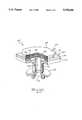
- FIG. 1is a perspective view, partially cutaway to reveal a cross-sectional view of a silicon capacitive pressure sensor having a glass dielectric spacer portion sputter-deposited onto a silicon substrate and then patterned to form the concentric rings of the present invention
- FIG. 2is a top plan view of a square-shaped silicon diaphragm having an octagon-shaped glass dielectric spacer disposed thereon and patterned to form a single ring, as in the prior art;
- FIG. 3is a top plan view of the square-shaped silicon diaphragm having an octagon-shaped dielectric glass spacer disposed thereon and patterned to form the pair of concentric rings, in accordance with the present invention.
- the sensor 100comprises a pair of parallel silicon capacitive plates (e.g., a diaphragm 104 and a substrate 108) separated by the borosilicate glass dielectric spacer 112 of the present invention.
- a silicon transition piece 116is also provided that attaches to the silicon substrate 108 by a second dielectric spacer 120.
- the transition piece 116has a throughbore 124 formed therein through which the fluid whose pressure is desired to be measured is applied to the diaphragm 104.
- the transition piece 116may be mounted on a header 128, and the entire sensor 100 is encapsulated in a standard package (not shown), for example, a T03 package. Electronic signal processing circuitry (not shown) may also be included within the package.
- FIG. 1there illustrated is a perspective view, partially cut away to expose in cross-sectional form a silicon capacitive pressure sensor 100.
- the sensor 100may be somewhat similar in structure to that described in the following U.S. patents, all assigned to the assignee of the present invention, and all hereby incorporated by reference: U.S. Pat. Nos. 4,879,627; 4,883,768; 4,951,174; 4,954,925; 4,513,348; 4,415,948 and 4,405,970.
- the sensor 100comprises a silicon diaphragm 104 and a silicon substrate 108, arranged in parallel and separated by a dielectric spacer 112.
- the spacer 112is typically made of borosilicate glass that may comprise, for example, the commercially available Model 7070 borosilicate glass supplied by Corning. However, the glass may comprise other commercially available brands of borosilicate glass, such as the Model 7740 borosilicate glass provided by Corning and sold under the trademark PYREX®. Alternatively, the glass may comprise, if desired, other types of glass, such as phosphosilicate.
- the sensor 100comprises a silicon-glass-silicon (“SGS”) sandwich that is typically square and/or octagonal in its exterior configuration, but often may be circular or cylindrical in shape for its inner, operative substructure.
- SGSsilicon-glass-silicon
- the diaphragm 104comprises a square sheet or plate of appropriately doped silicon, which is somewhat flexible.
- the substrate 108also comprises an appropriately doped sheet of silicon.
- the substrate 108is typically less flexible than the diaphragm 104.
- the dielectric spacer 112 disposed between the diaphragm 104 and substrate 108creates a closed, evacuated, hermetically-sealed chamber 132 between the two parallel silicon plates 104, 108.
- the chamber 132is typically held at a zero vacuum value, or, if desired, it can be sealed at a higher reference pressure.
- the pressure within the chamber 132depends upon the desired pressure value that the sensor 100 is designed to measure small variations or differential values therearound.
- the chamber 132thus provides a reference pressure on one side of the flexible diaphragm 104.
- a centrally-located, typically circular mesa 136is formed on a surface of the substrate 108.
- the mesa 136extends into the generally cylindrical chamber 132.
- the mesa 136serves as a counter-electrode to the flexible diaphragm 104.
- a thin insulating glass layer(not shown) may cover the top of the mesa 136.
- An upper surface of the mesa 136is illustrated as being planar. However, the mesa 136 may be non-planar (e.g., concave), as described and claimed in U.S. Pat. No. 5,381,299.
- the spacing between an undersurface of the silicon diaphragm 104 and the top of the mesa 136is approximately 2.5 microns, while the thickness of the borosilicate glass spacer 112 is typically 9 microns.
- the silicon diaphragm 104is approximately 8 thousandths (0.008") of an inch thick, while the substrate 108 is approximately fifty thousandths (0.050") of an inch thick.
- the diaphragm 104flexes toward the substrate 108. This causes the spacing between the diaphragm 104 and the substrate 108 to change. Since the diaphragm 104 and the substrate 108 serve as the plates of a parallel plate capacitor, the flexing of the diaphragm 104 inwardly increases the capacitance of the sensor 100. The change in capacitance as a result of the change in the pressure applied to the surface of the diaphragm 104 is used as a measure of the pressure applied to the sensor 100.
- a pair of electrical conductors or wires 140are connected to the diaphragm 104 and substrate 108 for connection to a well-known signal processing circuit (not shown), located external to the sensor 100.
- the circuitmay be located within the package (not shown) for the sensor 100.
- the circuittypically responds to the changing capacitance of the sensor 100 as a function of the applied pressure on the diaphragm 104.
- the varying pressure on the exterior, sensing surface of the flexible silicon diaphragm 104causes the diaphragm 104 to flex. Such flexing changes the value of the intersticial capacitance between the diaphragm 104 and the substrate 108, which transduces the applied pressure into a measurable electronic signal.
- the spacer 112is formed as a single ring, the wall of which typically has a horizontal thickness of, e.g., thirty-six thousandths (0.036") of an inch.
- the silicon diaphragm 104may typically be square, while the silicon substrate 108 may have octagonal shape. The octagonal shape of the substrate 108 provides access for attachment of the electrical wires 140 to the silicon diaphragm 104.
- FIG. 1the prior art sensor of FIG.
- the silicon substrate 108has a side length of two hundred sixty thousandths (0.260") of an inch, while the wall of the borosilicate glass spacer 112 has an inner diameter of one hundred ninety thousandths (0.190") of an inch.
- the outer side surface of the wall spacer 112can either follow the basic square configuration of the silicon diaphragm 104, or it may be octagonal, as illustrated in FIGS. 1 and 2, similar to the octagonal shape of the substrate 108.
- the mesa 136extends up from the silicon substrate 108 to a dimension of approximately 6.5 microns. The diameter of the mesa 136 may be one hundred fifty thousandths (0.150") of an inch.
- a transition piece 116is fabricated with the second borosilicate glass spacer 120 that, in turn, is bonded to the exterior surface of the silicon diaphragm 104.
- the glass spacer 120may also comprise the Model 7070 glass provided by Corning, or other suitable glass.
- the transition piece 116includes a pressure port 124, which comprises a throughbore, through which the fluid whose pressure is to be sensed is communicated to the exterior surface of the diaphragm 104.
- the transition piece 116tapers down to its pedestal shape for mounting to the surface of the header 128. The pedestal shape accommodates the temperature coefficient mismatch between the silicon and header material.
- the transition piece 116has a thickness of approximately one hundred twenty-five thousandths (0.125") of an inch.
- FIG. 3there illustrated is a top plan view of the silicon diaphragm 104 with the glass dielectric spacer 112 attached to a surface of the diaphragm 104 and patterned to form the pair of concentric rings 141, 142 in accordance with the present invention.
- the specific methodologies for forming the concentric rings 141, 142is described in greater detail hereinafter in FIGS. 4-8 with respect to the sequence of steps in fabricating the silicon capacitive pressure sensor 100.
- the inner ring 141is circular while the outer ring 142 is octagonal.
- the inside diameter of the circular inner ring 141may be approximately one hundred ninety thousandths (0.190") of an inch, similar to that of the prior art sensor of FIG.
- each ring 141, 142is uniform and is approximately one hundred fifty microns (slightly less than 6 mils; 0.006"). As can be seen from FIG. 3, the spacing between the rings 141, 142 varies due to the fact that the inner ring 141 is circular while the outer ring 142 is octagonal. The minimum amount of spacing between the rings 141, 142 is approximately six mils (0.006"). The aforementioned dimensions of the inner and outer rings 141, 142 results in a silicon substrate 108 with a somewhat smaller side length of approximately two hundred twenty-five thousandths (0.225") of an inch, compared to two hundred sixty thousandths (0.260") of an inch in the prior art design of FIG. 2.
- This reduced sizenot only reduces the parasitic capacitance, but it also increases the number of sensors that can be fabricated from a single silicon substrate wafer and a single silicon diaphragm wafer, with such processing being described in detail hereinafter with respect to FIGS. 4-8.
- the inner ring 141is circular for structural reasons in that the inner ring 141 approximates the circular nature of the inner, operative substructure of the sensor 100, such as the mesa 136.
- the outer ring 142is octagonal due to the fact that the silicon substrate 108 is also octagonal.
- the octagonal shape of both the substrate 108 and the outer ring 142is formed by dicing or sawing the substrate 108 and the outer ring 142. This removes portions of both the substrate 108 and the outer ring 142 to expose portions of the surface of the silicon diaphragm 104 for connection of the electrical wires 140 thereto.
- the dicing or sawingresults in contiguous planar outer surfaces of both the substrate 112 and the outer ring 142.
- the present inventionis not limited to having an octagonal-shape outer ring 142; other shapes may be used if desired. Further, other shapes may be used for the inner ring 141 as well, without departing from the broadest scope of the present invention.
- the rings 141, 142are described as being spaced apart from each other. However, it is to be understood that the two rings 141, 142 may be connected by some amount of glass dielectric spacer. In practice, it has been found that total separation between the two rings 141, 142 best facilitates the goal of reducing the parasitic capacitance of the sensor 100 as much as possible.
- the pair of rings of the present inventionreduces the proportion of the parasitic capacitance to the overall capacitance of the sensor 100 from approximately fifty (50) percent in the prior art design of FIG. 2 to approximately fifteen (15) percent in the concentric ring design of FIG. 3.
- FIGS. 4-8there illustrated in cross-sectional form is the sequence of steps in fabricating the sensor 100 of FIG. 1.
- the starting point in the fabrication processis a commercially-available silicon wafer 144 (FIG. 4) that comprises the substrate 108 of a fabricated sensor 100.
- the wafer 144is appropriately doped with, for example, antimony.
- the substrate wafer 144may either be doped with either N or P type impurities having a doping concentration of at least 10 15 impurity per cubic centimeter to achieve less than 1 ohm-centimeter resistivity.
- the substrate wafer 144is etched away at predetermined locations to create a plurality of mesas 136, each mesa 136 being approximately 6.5 microns in height.
- the glass that serves as the dielectric 112 between the diaphragm 104 and the substrate 108is deposited onto the silicon substrate wafer 144.
- the glass 112may be deposited onto the wafer 144 using any one of a number of well-known deposition techniques, such as vacuum deposition or sputtering.
- One sputter-deposition technique that may be used to deposit the glassis an ion-milling technique, as described and claimed in U.S. Pat. No. 5,375,034.
- the glass 112is deposited to a thickness of approximately 9 microns.
- the deposited glass 112serves three purposes: as a dielectric spacer 112 forming an enclosed vacuum chamber 132 between the conductive substrate 108 and conductive diaphragm 104; as a means of forming a precise gap between the diaphragm 104 and substrate 108; and as an agent for bonding the silicon substrate 108 and diaphragm 104 to the spacer 112.
- the glass 112comprises the Model 7070 borosilicate glass provided by Corning. This glass 112 has thermal properties (e.g., thermal expansion coefficients) similar to the silicon substrate 108. Also, this specific model of glass 112 has lithium and potassium ions that are available to assist in the bonding of the diaphragm 104 to the glass spacer 112, as described in greater detail hereinafter.
- the glassmay comprise other commercially available brands of borosilicate glass, such as Model 7740 borosilicate glass provided by Corning and sold under the trademark PYREX®.
- the glassmay comprise, if desired, other types of glass, such as phosphosilicate.
- the type of glass utilizedis based in part on the type(s) of alkali contained in the glass.
- the next step in the process of fabricating the silicon capacitive pressure sensor 100is that the silicon substrate wafer 144 with the glass spacer 112 formed thereon in bulk may be subject to thermal processing, such as annealing, to reduce any stresses in the glass.
- the silicon substrate wafer 144may be subject to a thermal processing procedure described and claimed in copending U.S. Patent Application entitled "Thermal Processing of Deposited Glass", filed Dec. 21, 1993, Ser. No. 08/188,952, and assigned to the same assignee as the present invention.
- thermal processing of the glassensures that any gas particles which are formed inherent in the glass as a result of a sputter-deposition process will diffuse out of the glass, and thus will not contribute to any long-term drift of the sensor.
- the thermal processensures that no undesirable and ruinous internal cavities (i.e., "bubbles" will be formed in the glass as a result of other prior art thermal processing procedures.
- the borosilicate glass layer 112is appropriately etched or patterned (FIG. 6) using well-known photolithography and etching techniques. This forms the pair of concentric glass rings 141, 142 in accordance with the present invention. These patterning techniques also form the glass spacer 112 only around the approximate perimeter of that portion of the silicon substrate wafer 144 that comprises the substrate 108 of the fabricated sensor 100.
- a second silicon wafer 160may be prepared, by suitable lapping to a desired thickness, such as on the order of 200 microns (i.e., approximately eight mils (0.008")), to form the flexible diaphragm 104 (see FIG. 7).
- the silicon diaphragm wafer 160may be appropriately doped with the desired impurities.
- the silicon diaphragm wafer 160is then bonded to the dielectric glass spacer 112 using known electrostatic bonding techniques.
- the diaphragm wafer 160may be bonded using the known field-assisted sealing technique of joining glass to semiconductors.
- This techniqueinvolves subjecting the diaphragm wafer 160 to temperatures of approximately 300°-500° C. to induce ionic mobility within the borosilicate glass.
- the aforementioned Model 7070 glass from Corninghas lithium and potassium ions available at high temperature that may be used in this electrostatic bonding technique.
- the glass spacer and diaphragm junctionis then subjected to an electric potential on the order of 100 volts DC. This produces a depletion layer at the interface between the silicon and the glass. If the electric potential is properly directed, the positive lithium and potassium ions drift away from the interface and a high field is created across this interface. This causes intimate contact between the glass spacer 112 and the silicon diaphragm wafer 160. In this manner, a hermetic seal between the silicon and glass is formed.
- This above-described processis normally accomplished in a vacuum in order to provide an absolute pressure sensor.
- Both the silicon substrate wafer 144 and silicon diaphragm wafer 160may have a thin metallization layer deposited locally thereon, for example, a layer of about five thousand angstroms of aluminum. This provides a suitable surface for wire bonding of the electrical wires 140 to both the diaphragm 104 and the substrate 108.
- This silicon wafercomprises the transition piece 116 of a fabricated sensor 100. More particularly, the wafer 164 has the desired transition pieces 116 formed at appropriate locations in the wafer by forming the pedestal-shaped outer surface and the throughbores 124 therein.
- the pedestal shapes and throughbores 124may be etched in the transition piece silicon wafer 164 using various techniques. For example, the shapes and throughbores 124 may be formed in the transition piece using the electrical discharge machining ("EDM") techniques described and claimed in copending U.S. patent application entitled “Fabricating Complex Silicon Pieces Using Electrical Discharge Machining", filed Dec. 2, 1993, Ser. No. 08/161,156, and assigned to the same assignee as the present invention.
- the transition piece wafer 164may be on the order of one hundred twenty-five thousandths (0.125") of an inch thick.
- the transition piece wafer 164then has a layer 120 of dielectric glass deposited thereon.
- the glass deposited onto the silicon wafer 164may also comprise the Model 7070 borosilicate glass from Corning.
- the glass layer 120may be deposited in an identical manner as the glass spacer 112 deposited onto the silicon substrate 108.
- the second glass layer 120is photolithographically patterned and etched into a ring only around the perimeter of the resulting transition piece 116.
- the glass layer 120is then bonded to the silicon diaphragm wafer 160 using electrostatic bonding techniques.
- the glass layer 120contacts the diaphragm wafer 160, as illustrated in FIG. 8.
- the resulting silicon and glass multi-layered componentis diced appropriately, such as by sawing, to provide a plurality of individual piece parts, as indicated by the phantom lines 168.
- both the silicon substrate 108 and the glass spacer 112may, if desired, be cut into an octagon shape to expose the electrical connection points on the silicon diaphragm 104.
- the individual piece part silicon capacitive pressure sensor 100may then be mounted to a surface of the header 128 (FIG. 1).
- the headermay comprise a material sold under the trademark KOVAR®, or other similar alloys.
- the headerhas a throughbore 172 that acts as a pressure port through which the fluid whose pressure is desired to be measured by the sensor 100 is applied thereto.
- the throughbore 124 of the transition piece 116is aligned over the pressure port 172 such that the transition piece 116 is in contact with the surface of the header 128.
- the transition piece 116is then bonded to the header 128 using an eutectic bonding process. This process involves coating with gold the outer surface of the silicon transition piece 116 that is to contact the header 128.
- the sensor 100 and the header 128are heated at an elevated temperature to bond the sensor 100 to the header 128.
Landscapes
- Physics & Mathematics (AREA)
- General Physics & Mathematics (AREA)
- Measuring Fluid Pressure (AREA)
- Pressure Sensors (AREA)
Abstract
Description
Claims (20)
Priority Applications (7)
| Application Number | Priority Date | Filing Date | Title |
|---|---|---|---|
| US08/188,257US5448444A (en) | 1994-01-28 | 1994-01-28 | Capacitive pressure sensor having a reduced area dielectric spacer |
| EP95909337AEP0742893B1 (en) | 1994-01-28 | 1995-01-26 | A capacitive pressure sensor having a reduced area dielectric spacer |
| ES95909337TES2133739T3 (en) | 1994-01-28 | 1995-01-26 | CAPACITIVE PRESSURE SENSOR WITH A DIELECTRIC DISTANCING ELEMENT WITH REDUCED SURFACE. |
| DE69509751TDE69509751T2 (en) | 1994-01-28 | 1995-01-26 | CAPACITIVE PRESSURE SENSOR WITH A DIELECTRIC DISTANCE PIECE WITH AREA LIMITED |
| PCT/US1995/001034WO1995020754A1 (en) | 1994-01-28 | 1995-01-26 | A capacitive pressure sensor having a reduced area dielectric spacer |
| AU17329/95AAU1732995A (en) | 1994-01-28 | 1995-01-26 | A capacitive pressure sensor having a reduced area dielectric spacer |
| CA002182180ACA2182180A1 (en) | 1994-01-28 | 1995-01-26 | A capacitive pressure sensor having a reduced area dielectric spacer |
Applications Claiming Priority (1)
| Application Number | Priority Date | Filing Date | Title |
|---|---|---|---|
| US08/188,257US5448444A (en) | 1994-01-28 | 1994-01-28 | Capacitive pressure sensor having a reduced area dielectric spacer |
Publications (1)
| Publication Number | Publication Date |
|---|---|
| US5448444Atrue US5448444A (en) | 1995-09-05 |
Family
ID=22692406
Family Applications (1)
| Application Number | Title | Priority Date | Filing Date |
|---|---|---|---|
| US08/188,257Expired - Fee RelatedUS5448444A (en) | 1994-01-28 | 1994-01-28 | Capacitive pressure sensor having a reduced area dielectric spacer |
Country Status (7)
| Country | Link |
|---|---|
| US (1) | US5448444A (en) |
| EP (1) | EP0742893B1 (en) |
| AU (1) | AU1732995A (en) |
| CA (1) | CA2182180A1 (en) |
| DE (1) | DE69509751T2 (en) |
| ES (1) | ES2133739T3 (en) |
| WO (1) | WO1995020754A1 (en) |
Cited By (18)
| Publication number | Priority date | Publication date | Assignee | Title |
|---|---|---|---|---|
| EP0794558A1 (en)* | 1996-02-26 | 1997-09-10 | Ford Motor Company | Hermetic seal for an electronic component having a secondary chamber |
| US6002487A (en)* | 1995-06-20 | 1999-12-14 | Nikon Corporation | Alignment method for performing alignment between shot areas on a wafer |
| US6003381A (en)* | 1998-10-16 | 1999-12-21 | Mitsubishi Denki Kabushiki Kaisha | Pressure sensor |
| US6143583A (en)* | 1998-06-08 | 2000-11-07 | Honeywell, Inc. | Dissolved wafer fabrication process and associated microelectromechanical device having a support substrate with spacing mesas |
| US6647794B1 (en)* | 2002-05-06 | 2003-11-18 | Rosemount Inc. | Absolute pressure sensor |
| US20070222009A1 (en)* | 2006-03-24 | 2007-09-27 | Infineon Technologies Sensonor As | Integrated Pedestal Mount for MEMS Structure |
| US20080000770A1 (en)* | 2006-06-29 | 2008-01-03 | Applied Materials, Inc. | Vacuum elastomer bonding apparatus and method |
| US20100230766A1 (en)* | 2009-03-12 | 2010-09-16 | Infineon Technologies Ag | Sensor device and method |
| US7819014B1 (en)* | 2009-04-23 | 2010-10-26 | Rosemount Inc. | Capacitive gage pressure sensor with vacuum dielectric |
| US20140251030A1 (en)* | 2013-03-07 | 2014-09-11 | Wico Hopman | Pressure transducer substrate with self alignment feature |
| US10323998B2 (en) | 2017-06-30 | 2019-06-18 | Sensata Technologies, Inc. | Fluid pressure sensor |
| EP3534126A3 (en)* | 2018-02-13 | 2019-11-13 | STMicroelectronics S.r.l. | Sensing device, in particular load sensing device |
| US10488289B2 (en) | 2016-04-11 | 2019-11-26 | Sensata Technologies, Inc. | Pressure sensors with plugs for cold weather protection and methods for manufacturing the plugs |
| US10545064B2 (en) | 2017-05-04 | 2020-01-28 | Sensata Technologies, Inc. | Integrated pressure and temperature sensor |
| US10557770B2 (en) | 2017-09-14 | 2020-02-11 | Sensata Technologies, Inc. | Pressure sensor with improved strain gauge |
| US10724907B2 (en) | 2017-07-12 | 2020-07-28 | Sensata Technologies, Inc. | Pressure sensor element with glass barrier material configured for increased capacitive response |
| EP1495491B1 (en)* | 2002-04-15 | 2020-12-16 | Schott AG | Method for connecting substrates and composite element |
| US10871413B2 (en) | 2016-04-20 | 2020-12-22 | Sensata Technologies, Inc. | Method of manufacturing a pressure sensor |
Families Citing this family (2)
| Publication number | Priority date | Publication date | Assignee | Title |
|---|---|---|---|---|
| GB9425250D0 (en)* | 1994-12-14 | 1995-02-08 | Otter Controls Ltd | Silicon capacitive pressure sensor designed for manufacturability and low long term drift |
| US6894383B2 (en)* | 2003-03-31 | 2005-05-17 | Intel Corporation | Reduced substrate micro-electro-mechanical systems (MEMS) device and system for producing the same |
Citations (15)
| Publication number | Priority date | Publication date | Assignee | Title |
|---|---|---|---|---|
| US4287553A (en)* | 1980-06-06 | 1981-09-01 | The Bendix Corporation | Capacitive pressure transducer |
| DE3137219A1 (en)* | 1981-09-18 | 1983-04-07 | Robert Bosch Gmbh, 7000 Stuttgart | Capacitive pressure sensor and method for producing it |
| US4405970A (en)* | 1981-10-13 | 1983-09-20 | United Technologies Corporation | Silicon-glass-silicon capacitive pressure transducer |
| US4415948A (en)* | 1981-10-13 | 1983-11-15 | United Technologies Corporation | Electrostatic bonded, silicon capacitive pressure transducer |
| US4467394A (en)* | 1983-08-29 | 1984-08-21 | United Technologies Corporation | Three plate silicon-glass-silicon capacitive pressure transducer |
| US4513348A (en)* | 1984-01-13 | 1985-04-23 | United Technologies Corporation | Low parasitic capacitance pressure transducer and etch stop method |
| US4517622A (en)* | 1983-08-29 | 1985-05-14 | United Technologies Corporation | Capacitive pressure transducer signal conditioning circuit |
| US4530029A (en)* | 1984-03-12 | 1985-07-16 | United Technologies Corporation | Capacitive pressure sensor with low parasitic capacitance |
| US4743836A (en)* | 1985-12-06 | 1988-05-10 | United Technologies Corporation | Capacitive circuit for measuring a parameter having a linear output voltage |
| US4879627A (en)* | 1988-12-30 | 1989-11-07 | United Technologies Corporation | Differential capacitive pressure sensor with over-pressure protection |
| US4883768A (en)* | 1989-02-28 | 1989-11-28 | United Technologies Corporation | Mesa fabrication in semiconductor structures |
| US4951174A (en)* | 1988-12-30 | 1990-08-21 | United Technologies Corporation | Capacitive pressure sensor with third encircling plate |
| US4954925A (en)* | 1988-12-30 | 1990-09-04 | United Technologies Corporation | Capacitive sensor with minimized dielectric drift |
| US5044202A (en)* | 1989-09-18 | 1991-09-03 | Texas Instruments Incorporated | Pressure transducer apparatus |
| JPH03239940A (en)* | 1990-02-16 | 1991-10-25 | Toyoda Mach Works Ltd | capacitive pressure sensor |
Family Cites Families (1)
| Publication number | Priority date | Publication date | Assignee | Title |
|---|---|---|---|---|
| US5134887A (en)* | 1989-09-22 | 1992-08-04 | Bell Robert L | Pressure sensors |
- 1994
- 1994-01-28USUS08/188,257patent/US5448444A/ennot_activeExpired - Fee Related
- 1995
- 1995-01-26WOPCT/US1995/001034patent/WO1995020754A1/enactiveIP Right Grant
- 1995-01-26CACA002182180Apatent/CA2182180A1/ennot_activeAbandoned
- 1995-01-26DEDE69509751Tpatent/DE69509751T2/ennot_activeExpired - Fee Related
- 1995-01-26EPEP95909337Apatent/EP0742893B1/ennot_activeExpired - Lifetime
- 1995-01-26ESES95909337Tpatent/ES2133739T3/ennot_activeExpired - Lifetime
- 1995-01-26AUAU17329/95Apatent/AU1732995A/ennot_activeAbandoned
Patent Citations (15)
| Publication number | Priority date | Publication date | Assignee | Title |
|---|---|---|---|---|
| US4287553A (en)* | 1980-06-06 | 1981-09-01 | The Bendix Corporation | Capacitive pressure transducer |
| DE3137219A1 (en)* | 1981-09-18 | 1983-04-07 | Robert Bosch Gmbh, 7000 Stuttgart | Capacitive pressure sensor and method for producing it |
| US4405970A (en)* | 1981-10-13 | 1983-09-20 | United Technologies Corporation | Silicon-glass-silicon capacitive pressure transducer |
| US4415948A (en)* | 1981-10-13 | 1983-11-15 | United Technologies Corporation | Electrostatic bonded, silicon capacitive pressure transducer |
| US4517622A (en)* | 1983-08-29 | 1985-05-14 | United Technologies Corporation | Capacitive pressure transducer signal conditioning circuit |
| US4467394A (en)* | 1983-08-29 | 1984-08-21 | United Technologies Corporation | Three plate silicon-glass-silicon capacitive pressure transducer |
| US4513348A (en)* | 1984-01-13 | 1985-04-23 | United Technologies Corporation | Low parasitic capacitance pressure transducer and etch stop method |
| US4530029A (en)* | 1984-03-12 | 1985-07-16 | United Technologies Corporation | Capacitive pressure sensor with low parasitic capacitance |
| US4743836A (en)* | 1985-12-06 | 1988-05-10 | United Technologies Corporation | Capacitive circuit for measuring a parameter having a linear output voltage |
| US4879627A (en)* | 1988-12-30 | 1989-11-07 | United Technologies Corporation | Differential capacitive pressure sensor with over-pressure protection |
| US4951174A (en)* | 1988-12-30 | 1990-08-21 | United Technologies Corporation | Capacitive pressure sensor with third encircling plate |
| US4954925A (en)* | 1988-12-30 | 1990-09-04 | United Technologies Corporation | Capacitive sensor with minimized dielectric drift |
| US4883768A (en)* | 1989-02-28 | 1989-11-28 | United Technologies Corporation | Mesa fabrication in semiconductor structures |
| US5044202A (en)* | 1989-09-18 | 1991-09-03 | Texas Instruments Incorporated | Pressure transducer apparatus |
| JPH03239940A (en)* | 1990-02-16 | 1991-10-25 | Toyoda Mach Works Ltd | capacitive pressure sensor |
Cited By (29)
| Publication number | Priority date | Publication date | Assignee | Title |
|---|---|---|---|---|
| US6002487A (en)* | 1995-06-20 | 1999-12-14 | Nikon Corporation | Alignment method for performing alignment between shot areas on a wafer |
| EP0794558A1 (en)* | 1996-02-26 | 1997-09-10 | Ford Motor Company | Hermetic seal for an electronic component having a secondary chamber |
| US5837935A (en)* | 1996-02-26 | 1998-11-17 | Ford Motor Company | Hermetic seal for an electronic component having a secondary chamber |
| US6143583A (en)* | 1998-06-08 | 2000-11-07 | Honeywell, Inc. | Dissolved wafer fabrication process and associated microelectromechanical device having a support substrate with spacing mesas |
| US6639289B1 (en) | 1998-06-08 | 2003-10-28 | Honeywell International Inc. | Dissolved wafer fabrication process and associated microelectromechanical device having a support substrate with spacing mesas |
| US6003381A (en)* | 1998-10-16 | 1999-12-21 | Mitsubishi Denki Kabushiki Kaisha | Pressure sensor |
| EP1495491B1 (en)* | 2002-04-15 | 2020-12-16 | Schott AG | Method for connecting substrates and composite element |
| US6647794B1 (en)* | 2002-05-06 | 2003-11-18 | Rosemount Inc. | Absolute pressure sensor |
| US20070222009A1 (en)* | 2006-03-24 | 2007-09-27 | Infineon Technologies Sensonor As | Integrated Pedestal Mount for MEMS Structure |
| US20080000770A1 (en)* | 2006-06-29 | 2008-01-03 | Applied Materials, Inc. | Vacuum elastomer bonding apparatus and method |
| US7476289B2 (en) | 2006-06-29 | 2009-01-13 | Applied Materials, Inc. | Vacuum elastomer bonding apparatus and method |
| US8373240B2 (en) | 2009-03-12 | 2013-02-12 | Infineon Technologies Ag | Sensor device having a structure element |
| US20100230766A1 (en)* | 2009-03-12 | 2010-09-16 | Infineon Technologies Ag | Sensor device and method |
| US8124953B2 (en) | 2009-03-12 | 2012-02-28 | Infineon Technologies Ag | Sensor device having a porous structure element |
| US8652866B2 (en) | 2009-03-12 | 2014-02-18 | Infineon Technologies Ag | Sensor device and method |
| US7819014B1 (en)* | 2009-04-23 | 2010-10-26 | Rosemount Inc. | Capacitive gage pressure sensor with vacuum dielectric |
| US20100269594A1 (en)* | 2009-04-23 | 2010-10-28 | Rosemount Inc. | Capacitive gage pressure sensor with vacuum dielectric |
| US20140251030A1 (en)* | 2013-03-07 | 2014-09-11 | Wico Hopman | Pressure transducer substrate with self alignment feature |
| US9146164B2 (en)* | 2013-03-07 | 2015-09-29 | Sensata Technologies, Inc. | Pressure transducer substrate with self alignment feature |
| US10488289B2 (en) | 2016-04-11 | 2019-11-26 | Sensata Technologies, Inc. | Pressure sensors with plugs for cold weather protection and methods for manufacturing the plugs |
| US10871413B2 (en) | 2016-04-20 | 2020-12-22 | Sensata Technologies, Inc. | Method of manufacturing a pressure sensor |
| US10545064B2 (en) | 2017-05-04 | 2020-01-28 | Sensata Technologies, Inc. | Integrated pressure and temperature sensor |
| US11105698B2 (en) | 2017-05-04 | 2021-08-31 | Sensata Technologies, Inc. | Method of assembling a sensing device having a double clinch seal |
| US10323998B2 (en) | 2017-06-30 | 2019-06-18 | Sensata Technologies, Inc. | Fluid pressure sensor |
| US10969288B2 (en) | 2017-06-30 | 2021-04-06 | Sensata Technologies, Inc. | Fluid pressure sensor |
| US10724907B2 (en) | 2017-07-12 | 2020-07-28 | Sensata Technologies, Inc. | Pressure sensor element with glass barrier material configured for increased capacitive response |
| US10557770B2 (en) | 2017-09-14 | 2020-02-11 | Sensata Technologies, Inc. | Pressure sensor with improved strain gauge |
| EP3534126A3 (en)* | 2018-02-13 | 2019-11-13 | STMicroelectronics S.r.l. | Sensing device, in particular load sensing device |
| US10910500B2 (en) | 2018-02-13 | 2021-02-02 | Stmicroelectronics S.R.L. | Load sensing devices, packages, and systems |
Also Published As
| Publication number | Publication date |
|---|---|
| WO1995020754A1 (en) | 1995-08-03 |
| ES2133739T3 (en) | 1999-09-16 |
| DE69509751T2 (en) | 1999-11-11 |
| DE69509751D1 (en) | 1999-06-24 |
| CA2182180A1 (en) | 1995-08-03 |
| EP0742893B1 (en) | 1999-05-19 |
| EP0742893A1 (en) | 1996-11-20 |
| AU1732995A (en) | 1995-08-15 |
Similar Documents
| Publication | Publication Date | Title |
|---|---|---|
| US5381299A (en) | Capacitive pressure sensor having a substrate with a curved mesa | |
| US5448444A (en) | Capacitive pressure sensor having a reduced area dielectric spacer | |
| KR0137939B1 (en) | Capacitive pressure sensor and method for minimizing the parasitic capacitance in a capacitive pressure sensor | |
| JP2517467B2 (en) | Capacitive pressure sensor | |
| JP3114570B2 (en) | Capacitive pressure sensor | |
| KR0137965B1 (en) | Capacitive sensor with minimized dielectric drift | |
| US6051853A (en) | Semiconductor pressure sensor including reference capacitor on the same substrate | |
| US4405970A (en) | Silicon-glass-silicon capacitive pressure transducer | |
| US7057247B2 (en) | Combined absolute differential transducer | |
| JPH0533732B2 (en) | ||
| US6595066B1 (en) | Stopped leadless differential sensor | |
| JPH0823564B2 (en) | Accelerometer having fine mechanism and manufacturing method thereof | |
| EP0385574A1 (en) | Capacitive semiconductor sensor with hinged diaphragm for planar movement | |
| EP0376631A1 (en) | Differential capacitive pressure sensor with over-pressure protection and method of providing over-pressure protection to a capacitive pressure sensor | |
| JPH0750789B2 (en) | Method for manufacturing semiconductor pressure converter | |
| JPH0623782B2 (en) | Capacitance type acceleration sensor and semiconductor pressure sensor | |
| US4531267A (en) | Method for forming a pressure sensor | |
| US4445384A (en) | Piezoelectric pressure sensor | |
| JPS6356935B2 (en) | ||
| JPH0565015B2 (en) | ||
| EP0633459B1 (en) | Capacitive pressure transducer structure and method for manufacturing the same | |
| CN108362408B (en) | Pressure sensor and method of making the same | |
| US5444901A (en) | Method of manufacturing silicon pressure sensor having dual elements simultaneously mounted | |
| US5440931A (en) | Reference element for high accuracy silicon capacitive pressure sensor | |
| CA1154502A (en) | Semiconductor variable capacitance pressure transducer |
Legal Events
| Date | Code | Title | Description |
|---|---|---|---|
| AS | Assignment | Owner name:UNITED TECHNOLOGIES CORPORATION, CONNECTICUT Free format text:ASSIGNMENT OF ASSIGNORS INTEREST;ASSIGNORS:PROVENZANO, PAUL L.;SWINDAL, JAMES L.;KUHLBERG, ROBERT J.;AND OTHERS;REEL/FRAME:006968/0558;SIGNING DATES FROM 19940120 TO 19940125 | |
| AS | Assignment | Owner name:BREED AUTOMOTIVE TECHNOLOGY, INC., FLORIDA Free format text:ASSIGNMENT OF ASSIGNORS INTEREST;ASSIGNOR:UNITED TECHNOLOGIES CORPORATION;REEL/FRAME:007690/0031 Effective date:19951020 | |
| CC | Certificate of correction | ||
| FEPP | Fee payment procedure | Free format text:PAYOR NUMBER ASSIGNED (ORIGINAL EVENT CODE: ASPN); ENTITY STATUS OF PATENT OWNER: LARGE ENTITY | |
| FPAY | Fee payment | Year of fee payment:4 | |
| AS | Assignment | Owner name:CONGRESS FINANCIAL CORPORATION (FLORIDA), FLORIDA Free format text:SECURITY INTEREST;ASSIGNOR:BREED AUTOMOTIVE TECHNOLOGY, INC.;REEL/FRAME:011442/0646 Effective date:20001226 | |
| AS | Assignment | Owner name:VTI HOLDING OY, FINLAND Free format text:ASSIGNMENT OF ASSIGNORS INTEREST;ASSIGNOR:BREED AUTOMOTIVE TECHNOLOGY, INC.;REEL/FRAME:013496/0133 Effective date:20020809 | |
| FPAY | Fee payment | Year of fee payment:8 | |
| REMI | Maintenance fee reminder mailed | ||
| AS | Assignment | Owner name:BREED AUTOMOTIVE TECHNOLOGY, INC., MICHIGAN Free format text:RELEASE OF SECURITY INTEREST IN TRADEMARKS;ASSIGNOR:CONGRESS FINANCIAL CORPORATION;REEL/FRAME:014313/0243 Effective date:20030725 | |
| REMI | Maintenance fee reminder mailed | ||
| LAPS | Lapse for failure to pay maintenance fees | ||
| STCH | Information on status: patent discontinuation | Free format text:PATENT EXPIRED DUE TO NONPAYMENT OF MAINTENANCE FEES UNDER 37 CFR 1.362 | |
| FP | Lapsed due to failure to pay maintenance fee | Effective date:20070905 |