US5448186A - Field-programmable gate array - Google Patents
Field-programmable gate arrayDownload PDFInfo
- Publication number
- US5448186A US5448186AUS08/214,135US21413594AUS5448186AUS 5448186 AUS5448186 AUS 5448186AUS 21413594 AUS21413594 AUS 21413594AUS 5448186 AUS5448186 AUS 5448186A
- Authority
- US
- United States
- Prior art keywords
- logic
- signal
- programmable gate
- gate array
- field
- Prior art date
- Legal status (The legal status is an assumption and is not a legal conclusion. Google has not performed a legal analysis and makes no representation as to the accuracy of the status listed.)
- Expired - Lifetime
Links
- 238000010586diagramMethods0.000description18
- 238000012986modificationMethods0.000description2
- 230000004048modificationEffects0.000description2
- 238000003491arrayMethods0.000description1
- 230000008054signal transmissionEffects0.000description1
Images


Classifications
- H—ELECTRICITY
- H03—ELECTRONIC CIRCUITRY
- H03K—PULSE TECHNIQUE
- H03K19/00—Logic circuits, i.e. having at least two inputs acting on one output; Inverting circuits
- H03K19/02—Logic circuits, i.e. having at least two inputs acting on one output; Inverting circuits using specified components
- H03K19/173—Logic circuits, i.e. having at least two inputs acting on one output; Inverting circuits using specified components using elementary logic circuits as components
- H03K19/177—Logic circuits, i.e. having at least two inputs acting on one output; Inverting circuits using specified components using elementary logic circuits as components arranged in matrix form
- H03K19/17736—Structural details of routing resources
- H—ELECTRICITY
- H03—ELECTRONIC CIRCUITRY
- H03K—PULSE TECHNIQUE
- H03K19/00—Logic circuits, i.e. having at least two inputs acting on one output; Inverting circuits
- H03K19/02—Logic circuits, i.e. having at least two inputs acting on one output; Inverting circuits using specified components
- H03K19/173—Logic circuits, i.e. having at least two inputs acting on one output; Inverting circuits using specified components using elementary logic circuits as components
- H03K19/177—Logic circuits, i.e. having at least two inputs acting on one output; Inverting circuits using specified components using elementary logic circuits as components arranged in matrix form
- H03K19/17724—Structural details of logic blocks
- H03K19/17728—Reconfigurable logic blocks, e.g. lookup tables
Definitions
- the inventionrelates to a field-programmable gate array which can be defined or redefined functions by a user.
- a field-programmable gate arrayhas a plurality of logic elements and is designed to obtain desirable logic functions by interconnecting the adjacent logic elements (e.g., see Frederick Furtek et al., "LABYRINTH: A Homogeneous Computational Medium", IEEE 1990 Custom Integrated Circuits Conference Proceedings, pp. 31.1.1-31.1.4, 1990; and Tapio Korpiharju et al., "TUTCA configurable logic cell array architecture", 1991 IEEE International ASIC Conference Proceedings, P3-3.1-P3-3.4, 1991).
- FIG. 8shows a way of interconnecting "local" signal lines which is common in the conventional field-programmable gate arrays disclosed in the above-mentioned two technical documents.
- reference numeral 50designates a logic element.
- FIG. 9is a diagram showing an internal architecture of the logic element.
- the logic element 50receives signals 51-a, 51-b, 51-c, 51-d from the four logic elements that are adjacent thereto up, down, right, and left, through signal lines, respectively, and outputs signals 53-a, 53-b, 53-c, 53-d through signal lines, respectively.
- the logic element 50includes four circuits 52-a, 52-b, 52-c, 52-d.
- the respective circuits 52-a, 52-b, 52-c, 52-dreceive the four signals 51-a, 51-b, 51-c, 51-d applied to the logic element 50 and outputs the upward signal 53-a, the downward signal 53-b, the leftward signal 53-c, and the rightward signal 53-d.
- FIG. 10shows a weighted mean circuit
- FIG. 11shows an adder.
- reference numeral 100designates a delay circuit; 101, an adder; 102, a divider; 103, a full adder; and 104, a half adder.
- each logic elementhas a function of a 1-bit full adder.
- FIG. 12shows interconnections for a single bit(surrounded by broken line) in the case of forming an n-bit adder by using the conventional field-programmable gate array.
- reference characters 50-a, 50-b, 50-c, 50-ddesignate logic elements, respectively; and 55, a partial circuit for a single bit of the n-bit adder.
- the logic elements 50-a and 50-bstore inputs A i , B i , respectively, and outputs these signals rightward.
- the logic element 50-coutputs an input from left directly downward and an input from below (carry-out signal CO i ) directly upward.
- the logic element 50-dreceives an input A i from above, an input B i from left, and an input CI i from below, adds these signals up, and outputs the sum S i rightward and the carry-out signal CO i upward.
- the n-bit adderrequires 4 ⁇ n logic elements.
- bit parallel logic operation unitswith an n-bit logic operation unit requiring 4 ⁇ n logic elements.
- the object of the inventionis to provide a field-programmable gate array capable of forming an adder, logic operation unit, or the like having a high utilization of logic elements.
- the inventionis applied to a field-programmable gate array that includes: regularly arrayed logic elements; a first group of signal lines interconnecting the logic elements adjacent to each other; and a second group of signal lines interconnecting the logic elements not adjacent to each other.
- FIG. 1is a diagram showing the interconnection of signal lines among logic elements of a field-programmable gate array, which is a first embodiment of the invention
- FIG. 2is a diagram showing an internal architecture of the logic element used in the field-programmable gate array shown in FIG. 1;
- FIG. 3a diagrams showing another internal architecture of the logic element
- FIG. 4is a diagram showing an architecture of a circuit for a single bit when a bit parallel adder is formed using the field-programmable gate array according to the invention
- FIG. 5is a diagram showing the interconnection of signal lines among logic elements of a field-programmable gate array, which is a second embodiment of the invention.
- FIGS. 6(a)-6(c)are diagrams showing a 4 ⁇ 4 bit parallel multiplier formed on the field-programmable gate array shown in FIG. 5;
- FIG. 7is a diagram showing an internal architecture of the field-programmable gate array shown in FIG. 5;
- FIG. 8is a diagram showing the interconnection of signal lines among logic elements of a conventional field-programmable gate array
- FIG. 9is a diagram showing an internal architecture of the logic element of the conventional field-programmable gate array.
- FIG. 10is a diagram showing an architecture of a weighted mean circuit
- FIG. 11is a diagram showing an architecture of an 8-bit adder.
- FIG. 12is a diagrams showing an architecture of a circuit for a single bit when a bit parallel adder is formed using the conventional field-programmable gate array.
- FIG. 1shows the interconnection of signal lines in a programmable gate array, which is a first embodiment of the present invention
- FIG. 2shows a logic element of the programmable gate array of FIG. 1 in block-diagram form.
- reference character 1designates a first logic element; 2-a to 2-d, input signals from second logic elements 2 that are adjacent to the logic element 1 up, down, right, and left; 2-e to 2-h, input signals from third logic elements 3 that are one logic element away from the logic element 1 up, down, right, and left one logic element away; 3-a to 3-h, circuits for outputting signals 4-a to 4-h; 4-a to 4-d, output signals to the second logic elements 2 that are adjacent to, the logic element 1 up, down, right, and left; and 4-e to 4-h, output signals to the third logic elements 3 that are one logic element away from the logic element 1 up, down, right, and left.
- the circuits 3-a to 3-hreceive input signals 2-a to 2-h, respectively, and include combinational circuits or sequential circuits.
- the circuits 3-a to 3-hmay be formed partially in common to reduce the size of hardware.
- An architecture of each of the logic elements in such a caseis shown in FIG. 3.
- the first, second and third logic elementshave a same architecture, respectively.
- reference numeral 20designates an 8-4 selector; 21 to 24, 16-bit RAMs; 25 to 28, 2-1 selectors; 29, a 1-bit latch; 30 to 33, 5-1 selectors; 34, a 25-bit register; and 35, a 4-2 selector.
- the 8-4 selector 20receives a 5-bit control signal from the 25-bit register 34 and outputs four signals selected from the inputs 2-a, 2-b, 2-c, 2-d, 2-e, 2-f, 2-g, and 2-h.
- Each of the 16-bit RAMs 21-24receives a 4-bit input, reads one bit out of the 4-bit input as an address, and outputs such 1-bit address.
- Each of the 2-1 selectors 25 to 28receives 1-bit selection signal from the 25-bit register 34 and outputs either the output of the corresponding 16-bit RAM or the output of the 1-bit latch 29 by selection.
- the 1-bit latch 29receives a 1-bit output of the 4-2 selector 35 and latches the input by the control of a clock input signal CLK and an input enable signal EN for the 1-bit output of the 4-2 selector 35.
- Each of the 5-1 selectors 30 to 33receives the outputs of the 16-bit RAMs 21 to 24 and the output of 1-bit latch 29, and outputs one bit by selection. This selection is controlled by a 3-bit selection signal received from the 25-bit resister 34.
- the 25-bit register 34outputs a control signal within the logic element.
- the 4-2 selector 35receives the outputs of the 16-bit RAMs 21 to 24, and outputs one bit by selection. This selection is controlled by a 4-bit selection signal received from the 25-bit register 34.
- the writing of data to the 16-bit RAMs 21 to 24 and the 25-bit register 34is performed by a writing unit which is not shown in FIG. 3.
- FIG. 4In the case of forming an n-bit adder using the field-programmable gate array, which is the first embodiment of the invention, signal lines for a single bit are interconnected is as shown in FIG. 4.
- reference characters 1-a, 1-b, 1-cdesignate first, second and third logic elements, respectively; and 7, a partial circuit for the single bit.
- the first logic element 1-astores an input A i of the adder, and outputs such input to the third logic element 1-c.
- the second logic element 1-bstores an input B i of the adder and outputs such input to the third logic element 1-c.
- the third logic element 1-creceives A i , B i from left and CI i from below.
- the third logic element 1-coutputs a sum S i rightward and a carry-out signal CO i upward. Therefore, a conventional n-bit parallel adder requiring 4 ⁇ n logic elements can be implemented by 3 ⁇ n logic elements, which contributes to reducing the number of logic elements.
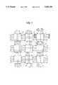
- FIG. 5shows the interconnection of signal lines of a programmable gate array, which is a second embodiment of the invention.
- reference numeral 1'designates a first logic element.
- the first logic element 1'is interconnected to four second adjacent logic elements 2' as well as upper right and lower left third logic elements 3' through input/output signal lines.
- the interconnection to the respective logic elements through the obliquely extending signal linesis useful in implementing a parallel multiplier on a field-programmable gate array. The following explains reasons therefor.
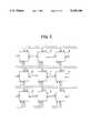
- FIGS. 6(a) to (c)are diagrams showing an architecture of a 4-bit ⁇ 4-bit parallel multiplier formed on the field-programmable gate array of FIG. 5.
- FIG. 6(a)is a diagram illustrative of input/output signals for a logic element
- FIG. 6(b)is a block diagram showing how logic elements are interconnected
- FIG. 6(c)is a diagram illustrative of an arrangement of logic elements 2-1 to 2-20.
- This multiplierreceives binary-coded numbers A (a3, a2, a1, a0) and B (b3, b2, b1, b0), and outputs a product P (p7, p6, p5, p4, p3, p2, p1, p0).
- a rightward inputis Ti and an output signal thereof is To;
- a leftward inputis Ui and an output signal thereof is Uo;
- an upward input signalis Vi and an output signal thereof is Vo;
- a downward input signalis Wi and an output signal thereof is Wo;
- an input signal directed to upper rightis Xi and an output signal thereof is Xo; and an input signal directed to lower left is Yi and an output signal thereof is Yo.
- the following input signalsare applied to the logic elements 2-1 to 2-20.
- Numbers a3, a2, a1, a0are inputted to the Xi signal lines of the logic elements 2-17, 2-18, 2-19, 2-20, respectively.
- the numbers b3, b2, b1, b0are inputted to the Ti signal lines of the logic elements 2-1, 2-5, 2-9, 2-13, respectively.
- the number 0is inputted to the Wi signal lines of the logic elements 2-1, 2-2, 2-3, 2-4, 2-5, 2-9, 2-13, 2-17, respectively.
- the products p7, p6, p5, p4, p3, p2, p1, p0are obtained from the Wo signal lines of the logic elements 2-17, 2-18, 2-19, 2-20, 2-16, 2-12, 2-8, 2-4, respectively.
- FIG. 7shows an internal architecture of each of the logic elements on the field-programmable gate array of FIG. 5.
- the first, second and third logic elementshave a same architecture, respectively.
- reference numeral 36designates a 6-4 selector; 21 to 24, 16-bit RAMs; 25 to 28, 2-1 selectors; 29, a 1-bit latch; 30 and 31, 5-1 selectors; 37, an 18-bit register; and 35, a 4-2 selector.
- the 6-4 selector 36receives a 4-bit control signal from the 18-bit register 37, and outputs four inputs selected from inputs Ti, Ui, Vi, Wi, Xi, Yi.
- Each of the 16-bit RAMs 21 to 24receives a 4-bit input, reads one bit out of the 4-bit input as an address, and outputs such 1-bit address.
- Each of the 2-1 selectors 25 to 28receives a 1-bit selection signal from the 18-bit register 37, and outputs either the output of the corresponding 16-bit RAM or the output of the 1-bit latch 29 by selection.
- the 1-bit latch 29receives a 1-bit output of the 4-2 selector 35 and latches the input by the control of a clock input signal CLK and an input enable signal EN for the 1-bit output of the 4-2 selector 35.
- Each of the 5-1 selectors 30 and 31receives the outputs of the 16-bit RAMs 21 to 24 and the output of the 1-bit latch 29, and outputs one bit by selection. This selection is controlled by a 3-bit selection signal received from the 18-bit register 37.
- the 18-bit register 37outputs a control signal within the logic element.
- the 4-2 selector 35receives the outputs of the 16-bit RAMs 21 to 24, and outputs one bit by selection. This selection is controlled by a 4-bit selection signal received from the 18-bit register 37.
- the writing of data to the 16-bit RAMs 21 to 24 and the 18-bit register 37is performed by a writing unit which is not shown in FIG. 7.
- the inventionprovides the advantage that a bit parallel logic operation unit can be implemented on the field-programmable gate array involving a smaller number of logic elements.
- the downsizing of the logic operation unitcontributes to implementing high speed processing with reduced signal transmission-induced delay.
Landscapes
- Physics & Mathematics (AREA)
- Mathematical Physics (AREA)
- Engineering & Computer Science (AREA)
- Computer Hardware Design (AREA)
- Computing Systems (AREA)
- General Engineering & Computer Science (AREA)
- Computer Networks & Wireless Communication (AREA)
- Logic Circuits (AREA)
Abstract
Description
1. Field of the Invention
The invention relates to a field-programmable gate array which can be defined or redefined functions by a user.
2. Description of the Related Art
A field-programmable gate array has a plurality of logic elements and is designed to obtain desirable logic functions by interconnecting the adjacent logic elements (e.g., see Frederick Furtek et al., "LABYRINTH: A Homogeneous Computational Medium", IEEE 1990 Custom Integrated Circuits Conference Proceedings, pp. 31.1.1-31.1.4, 1990; and Tapio Korpiharju et al., "TUTCA configurable logic cell array architecture", 1991 IEEE International ASIC Conference Proceedings, P3-3.1-P3-3.4, 1991).
Conventionally, when only "local" signal lines are used for the interconnection of logic elements of a field-programmable gate array, it is difficult to interconnect logic elements that are remote from each other (are not adjacent each other). Therefore, interconnection using only the "local" signal lines is considered inflexible. The term "local" is herein construed as specifying a signal line used to interconnect logic elements closest to each other. The feature of the "local" signal line is a smaller load capacity and line delay than other "global" signal lines (e.g., a clock signal line) and signal lines directlyinterconnecting logic elements that are remote each other.
FIG. 8 shows a way of interconnecting "local" signal lines which is common in the conventional field-programmable gate arrays disclosed in the above-mentioned two technical documents.
In FIG. 8,reference numeral 50 designates a logic element. FIG. 9 is a diagram showing an internal architecture of the logic element. Thelogic element 50 receives signals 51-a, 51-b, 51-c, 51-d from the four logic elements that are adjacent thereto up, down, right, and left, through signal lines, respectively, and outputs signals 53-a, 53-b, 53-c, 53-d through signal lines, respectively. As shown in FIG. 9, thelogic element 50 includes four circuits 52-a, 52-b, 52-c, 52-d. The respective circuits 52-a, 52-b, 52-c, 52-d receive the four signals 51-a, 51-b, 51-c, 51-d applied to thelogic element 50 and outputs the upward signal 53-a, the downward signal 53-b, the leftward signal 53-c, and the rightward signal 53-d.
The case of forming a weighted mean circuit and an adder will be described as the example of forming various circuits using the above-mentioned field-programmable gate array.
FIG. 10 shows a weighted mean circuit; and FIG. 11 shows an adder. In FIGS. 10 and 11,reference numeral 100 designates a delay circuit; 101, an adder; 102, a divider; 103, a full adder; and 104, a half adder.
As is apparent from FIG. 10, the signal flow in which two inputs to eachadder 101 enter from a single side and exit to a side opposite to such single side is reasonable in terms of the physical arrangement of the circuit and the principle of pipelining, and is therefore quite natural.
It is presumed to form an n-bit adder Using the conventional field-programmable gate array shown in FIG. 8. Here, each logic element has a function of a 1-bit full adder.
FIG. 12 shows interconnections for a single bit(surrounded by broken line) in the case of forming an n-bit adder by using the conventional field-programmable gate array. In FIG. 12, reference characters 50-a, 50-b, 50-c, 50-d designate logic elements, respectively; and 55, a partial circuit for a single bit of the n-bit adder. The logic elements 50-a and 50-b store inputs Ai, Bi, respectively, and outputs these signals rightward. The logic element 50-c outputs an input from left directly downward and an input from below (carry-out signal COi) directly upward. The logic element 50-d receives an input Ai from above, an input Bi from left, and an input CIi from below, adds these signals up, and outputs the sum Si rightward and the carry-out signal COi upward.
In the thus described architecture, the n-bit adder requires 4×n logic elements. The same applies to bit parallel logic operation units, with an n-bit logic operation unit requiring 4×n logic elements.
The problem encountered when such n-bit adder or logic operation unit is formed using the conventional field-programmable gate array is a low utilization of the logic elements.
Therefore, the object of the invention is to provide a field-programmable gate array capable of forming an adder, logic operation unit, or the like having a high utilization of logic elements.
To achieve the above object, the invention is applied to a field-programmable gate array that includes: regularly arrayed logic elements; a first group of signal lines interconnecting the logic elements adjacent to each other; and a second group of signal lines interconnecting the logic elements not adjacent to each other.
In the present invention, not only adjacent logic elements but also nonadjacent logic elements are interconnected to each other. Therefore, the number of logic elements used for merely allowing signals to pass therethrough is reduced. As a result, the utilization of the logic elements is improved, thereby contributing to implementing the same function with a smaller number of logic elements than before.
In the drawings:
FIG. 1 is a diagram showing the interconnection of signal lines among logic elements of a field-programmable gate array, which is a first embodiment of the invention;
FIG. 2 is a diagram showing an internal architecture of the logic element used in the field-programmable gate array shown in FIG. 1;
FIG. 3 a diagrams showing another internal architecture of the logic element;
FIG. 4 is a diagram showing an architecture of a circuit for a single bit when a bit parallel adder is formed using the field-programmable gate array according to the invention;
FIG. 5 is a diagram showing the interconnection of signal lines among logic elements of a field-programmable gate array, which is a second embodiment of the invention;
FIGS. 6(a)-6(c) are diagrams showing a 4×4 bit parallel multiplier formed on the field-programmable gate array shown in FIG. 5;
FIG. 7 is a diagram showing an internal architecture of the field-programmable gate array shown in FIG. 5;
FIG. 8 is a diagram showing the interconnection of signal lines among logic elements of a conventional field-programmable gate array;
FIG. 9 is a diagram showing an internal architecture of the logic element of the conventional field-programmable gate array;
FIG. 10 is a diagram showing an architecture of a weighted mean circuit;
FIG. 11 is a diagram showing an architecture of an 8-bit adder; and
FIG. 12 is a diagrams showing an architecture of a circuit for a single bit when a bit parallel adder is formed using the conventional field-programmable gate array.
The detailed embodiments of the present invention will now be described specifically accompanying with the drawings.
FIG. 1 shows the interconnection of signal lines in a programmable gate array, which is a first embodiment of the present invention; and FIG. 2 shows a logic element of the programmable gate array of FIG. 1 in block-diagram form.
In FIGS. 1 and 2,reference character 1 designates a first logic element; 2-a to 2-d, input signals fromsecond logic elements 2 that are adjacent to thelogic element 1 up, down, right, and left; 2-e to 2-h, input signals fromthird logic elements 3 that are one logic element away from thelogic element 1 up, down, right, and left one logic element away; 3-a to 3-h, circuits for outputting signals 4-a to 4-h; 4-a to 4-d, output signals to thesecond logic elements 2 that are adjacent to, thelogic element 1 up, down, right, and left; and 4-e to 4-h, output signals to thethird logic elements 3 that are one logic element away from thelogic element 1 up, down, right, and left. The circuits 3-a to 3-h receive input signals 2-a to 2-h, respectively, and include combinational circuits or sequential circuits.
The circuits 3-a to 3-h may be formed partially in common to reduce the size of hardware. An architecture of each of the logic elements in such a case is shown in FIG. 3. The first, second and third logic elements have a same architecture, respectively. In FIG. 3,reference numeral 20 designates an 8-4 selector; 21 to 24, 16-bit RAMs; 25 to 28, 2-1 selectors; 29, a 1-bit latch; 30 to 33, 5-1 selectors; 34, a 25-bit register; and 35, a 4-2 selector.
The 8-4selector 20 receives a 5-bit control signal from the 25-bit register 34 and outputs four signals selected from the inputs 2-a, 2-b, 2-c, 2-d, 2-e, 2-f, 2-g, and 2-h. Each of the 16-bit RAMs 21-24 receives a 4-bit input, reads one bit out of the 4-bit input as an address, and outputs such 1-bit address. Each of the 2-1selectors 25 to 28 receives 1-bit selection signal from the 25-bit register 34 and outputs either the output of the corresponding 16-bit RAM or the output of the 1-bit latch 29 by selection. The 1-bit latch 29 receives a 1-bit output of the 4-2selector 35 and latches the input by the control of a clock input signal CLK and an input enable signal EN for the 1-bit output of the 4-2selector 35. Each of the 5-1selectors 30 to 33 receives the outputs of the 16-bit RAMs 21 to 24 and the output of 1-bit latch 29, and outputs one bit by selection. This selection is controlled by a 3-bit selection signal received from the 25-bit resister 34. The 25-bit register 34 outputs a control signal within the logic element. The 4-2selector 35 receives the outputs of the 16-bit RAMs 21 to 24, and outputs one bit by selection. This selection is controlled by a 4-bit selection signal received from the 25-bit register 34. The writing of data to the 16-bit RAMs 21 to 24 and the 25-bit register 34 is performed by a writing unit which is not shown in FIG. 3.
In the case of forming an n-bit adder using the field-programmable gate array, which is the first embodiment of the invention, signal lines for a single bit are interconnected is as shown in FIG. 4. In FIG. 4, reference characters 1-a, 1-b, 1-c designate first, second and third logic elements, respectively; and 7, a partial circuit for the single bit. The first logic element 1-a stores an input Ai of the adder, and outputs such input to the third logic element 1-c. The second logic element 1-b stores an input Bi of the adder and outputs such input to the third logic element 1-c. The third logic element 1-c receives Ai, Bi from left and CIi from below. Further, the third logic element 1-c outputs a sum Si rightward and a carry-out signal COi upward. Therefore, a conventional n-bit parallel adder requiring 4×n logic elements can be implemented by 3×n logic elements, which contributes to reducing the number of logic elements.
A second embodiment of the invention will be described as follows. FIG. 5 shows the interconnection of signal lines of a programmable gate array, which is a second embodiment of the invention. In FIG. 5, reference numeral 1' designates a first logic element. In the second embodiment, the first logic element 1' is interconnected to four second adjacent logic elements 2' as well as upper right and lower left third logic elements 3' through input/output signal lines. The interconnection to the respective logic elements through the obliquely extending signal lines is useful in implementing a parallel multiplier on a field-programmable gate array. The following explains reasons therefor.
FIGS. 6(a) to (c) are diagrams showing an architecture of a 4-bit×4-bit parallel multiplier formed on the field-programmable gate array of FIG. 5. FIG. 6(a) is a diagram illustrative of input/output signals for a logic element; FIG. 6(b) is a block diagram showing how logic elements are interconnected; and FIG. 6(c) is a diagram illustrative of an arrangement of logic elements 2-1 to 2-20.
This multiplier receives binary-coded numbers A (a3, a2, a1, a0) and B (b3, b2, b1, b0), and outputs a product P (p7, p6, p5, p4, p3, p2, p1, p0). In thelogic element 2, a rightward input is Ti and an output signal thereof is To; a leftward input is Ui and an output signal thereof is Uo; an upward input signal is Vi and an output signal thereof is Vo; a downward input signal is Wi and an output signal thereof is Wo; an input signal directed to upper right is Xi and an output signal thereof is Xo; and an input signal directed to lower left is Yi and an output signal thereof is Yo.
Now, the following input signals are applied to the logic elements 2-1 to 2-20. Numbers a3, a2, a1, a0 are inputted to the Xi signal lines of the logic elements 2-17, 2-18, 2-19, 2-20, respectively. The numbers b3, b2, b1, b0 are inputted to the Ti signal lines of the logic elements 2-1, 2-5, 2-9, 2-13, respectively. Thenumber 0 is inputted to the Wi signal lines of the logic elements 2-1, 2-2, 2-3, 2-4, 2-5, 2-9, 2-13, 2-17, respectively.
As output signals, the products p7, p6, p5, p4, p3, p2, p1, p0 are obtained from the Wo signal lines of the logic elements 2-17, 2-18, 2-19, 2-20, 2-16, 2-12, 2-8, 2-4, respectively.
Functions to be implemented on each logic element is presented below.
______________________________________ i) Logic elements 2-1 to 2-16 Xo ← Xi, To ← Ti, Wo ← Wi XOR Yi XOR (Xi AND Ti), Yo ← Wi AND Yi OR Wi AND Xi AND Ti OR Yi AND Xi AND Ti ii) Logic elements 2-17 to 2-20 Xo ← Xi, To ← Ti, Wo ← Wi XOR Yi XOR (Xi AND Ti), Uo ← Wi AND Yi OR Wi AND Xi AND Ti OR Yi AND Xi AND Ti ______________________________________
FIG. 7 shows an internal architecture of each of the logic elements on the field-programmable gate array of FIG. 5. The first, second and third logic elements have a same architecture, respectively. In FIG. 7,reference numeral 36 designates a 6-4 selector; 21 to 24, 16-bit RAMs; 25 to 28, 2-1 selectors; 29, a 1-bit latch; 30 and 31, 5-1 selectors; 37, an 18-bit register; and 35, a 4-2 selector.
The 6-4selector 36 receives a 4-bit control signal from the 18-bit register 37, and outputs four inputs selected from inputs Ti, Ui, Vi, Wi, Xi, Yi. Each of the 16-bit RAMs 21 to 24 receives a 4-bit input, reads one bit out of the 4-bit input as an address, and outputs such 1-bit address. Each of the 2-1selectors 25 to 28 receives a 1-bit selection signal from the 18-bit register 37, and outputs either the output of the corresponding 16-bit RAM or the output of the 1-bit latch 29 by selection. The 1-bit latch 29 receives a 1-bit output of the 4-2selector 35 and latches the input by the control of a clock input signal CLK and an input enable signal EN for the 1-bit output of the 4-2selector 35. Each of the 5-1selectors bit RAMs 21 to 24 and the output of the 1-bit latch 29, and outputs one bit by selection. This selection is controlled by a 3-bit selection signal received from the 18-bit register 37. The 18-bit register 37 outputs a control signal within the logic element. The 4-2selector 35 receives the outputs of the 16-bit RAMs 21 to 24, and outputs one bit by selection. This selection is controlled by a 4-bit selection signal received from the 18-bit register 37. The writing of data to the 16-bit RAMs 21 to 24 and the 18-bit register 37 is performed by a writing unit which is not shown in FIG. 7.
As described in the foregoing, the invention provides the advantage that a bit parallel logic operation unit can be implemented on the field-programmable gate array involving a smaller number of logic elements. In addition, the downsizing of the logic operation unit contributes to implementing high speed processing with reduced signal transmission-induced delay.
The foregoing description of preferred embodiments of the invention has been presented for purposes of illustration and description. It is not intended to be exhaustive or to limit the invention to the precise form disclosed, and modifications and variations are possible in light of the above teachings or may be acquired from practice of the invention. The embodiments were chosen and described in order to explain the principles of the invention and its practical application to enable one skilled in the art to utilize the invention in various embodiments and with various modifications as are suited to the particular use contemplated. It is intended that the scope of the invention be defined by the claims appended hereto, and their equivalents.
Claims (10)
1. A field-programmable gate array comprising:
regularly arrayed logic elements;
a first group of signal lines regularly disposed and each interconnecting only one logic element and another logic element adjacent to the one logic element; and
a second group of signal lines regularly disposed and each interconnecting only one logic element and another logic element not adjacent to the one logic element.
2. A field-programmable gate array according to claim 1, wherein each of the logic elements has a logic circuit for outputting signals to the logic elements not adjacent thereto.
3. A field-programmable gate array according to claim 2, wherein the logic circuit for outputting signals outputs signals corresponding to input signals received through the first and the second groups of signal lines.
4. A field-programmable gate array comprising:
a first logic element; a plurality of second logic elements adjacent to the first logic element; and a plurality of third logic elements adjacent to the second logic elements;
each logic element having:
an input selector for selecting a predetermined number of input signals from a plurality of input signals;
logic circuit performing a logic function on the predetermined number of input signals;
a plurality of signal output means coupled to the logic circuit, each outputting a signal in response to the predetermined number of input signals;
selection and output means for selecting a signal outputted from one of the plurality of signal output means and outputting the selected signal;
a plurality of first output selectors, each being connected to one of the plurality of signal output means and the selection and output means;
a plurality of second output selectors, each being connected to all the plurality of signal output means and the selection and output means; and
control means for controlling each input and first and second output selectors and the selection and output means;
wherein the first output selector of the first logic element is connected to the input selector of each second logic element, and the second output selector of the first logic element is connected to the input selector of each third logic element.
5. A field-programmable gate array according to claim 4, wherein each of the logic elements has four signal output means, four first output selectors, and four second output selectors.
6. A field-programmable gate array according to claim 4, wherein each of the logic elements has four signal output means, four first output selectors, and two second output selectors.
7. A field-programmable gate array according to claim 4, wherein the logic elements, each being rectangular, are juxtaposed in the form of a cross.
8. A field-programmable gate array according to claim 4, wherein the first, second, and third logic elements are disposed in a diagonal arrangement.
9. A field-programmable gate array according to claim 4, wherein latching means latches the received signal by the control of a clock input signal and an input enable signal.
10. A field-programmable gate array according to claim 4, further comprising latching means connected to the selection and output means for receiving one of the signals outputted from the selection and output means, the latching means latching the one signal.
Applications Claiming Priority (2)
| Application Number | Priority Date | Filing Date | Title |
|---|---|---|---|
| JP5059083AJPH06276086A (en) | 1993-03-18 | 1993-03-18 | Field programmable gate array |
| JP5-059083 | 1993-03-18 |
Publications (1)
| Publication Number | Publication Date |
|---|---|
| US5448186Atrue US5448186A (en) | 1995-09-05 |
Family
ID=13103104
Family Applications (1)
| Application Number | Title | Priority Date | Filing Date |
|---|---|---|---|
| US08/214,135Expired - LifetimeUS5448186A (en) | 1993-03-18 | 1994-03-16 | Field-programmable gate array |
Country Status (2)
| Country | Link |
|---|---|
| US (1) | US5448186A (en) |
| JP (1) | JPH06276086A (en) |
Cited By (79)
| Publication number | Priority date | Publication date | Assignee | Title |
|---|---|---|---|---|
| US5537057A (en)* | 1995-02-14 | 1996-07-16 | Altera Corporation | Programmable logic array device with grouped logic regions and three types of conductors |
| US5570039A (en)* | 1995-07-27 | 1996-10-29 | Lucent Technologies Inc. | Programmable function unit as parallel multiplier cell |
| US5609096A (en)* | 1993-12-17 | 1997-03-11 | Goldstar Co., Ltd. | Vegetable freshness keeping device having a sensor |
| US5614840A (en)* | 1995-05-17 | 1997-03-25 | Altera Corporation | Programmable logic array integrated circuits with segmented, selectively connectable, long interconnection conductors |
| US5689195A (en)* | 1995-05-17 | 1997-11-18 | Altera Corporation | Programmable logic array integrated circuit devices |
| US5694058A (en)* | 1996-03-20 | 1997-12-02 | Altera Corporation | Programmable logic array integrated circuits with improved interconnection conductor utilization |
| US5701091A (en)* | 1995-05-02 | 1997-12-23 | Xilinx, Inc. | Routing resources for hierarchical FPGA |
| US5764076A (en)* | 1996-06-26 | 1998-06-09 | Xilinx, Inc. | Circuit for partially reprogramming an operational programmable logic device |
| US5825203A (en)* | 1995-11-28 | 1998-10-20 | Hitachi, Ltd. | Variable logic integrated circuit device having connections through switch matrix and top layers for inter-cell connections |
| US5835998A (en)* | 1996-04-04 | 1998-11-10 | Altera Corporation | Logic cell for programmable logic devices |
| US5872463A (en)* | 1996-04-04 | 1999-02-16 | Altera Corporation | Routing in programmable logic devices using shared distributed programmable logic connectors |
| US5880597A (en)* | 1996-09-18 | 1999-03-09 | Altera Corporation | Interleaved interconnect for programmable logic array devices |
| US5909126A (en)* | 1995-05-17 | 1999-06-01 | Altera Corporation | Programmable logic array integrated circuit devices with interleaved logic array blocks |
| WO1999034514A1 (en)* | 1997-12-29 | 1999-07-08 | Imperial College Of Science, Technology And Medicine | Logic circuit |
| US5936425A (en)* | 1995-05-17 | 1999-08-10 | Altera Corporation | Tri-statable input/output circuitry for programmable logic |
| US5943242A (en)* | 1995-11-17 | 1999-08-24 | Pact Gmbh | Dynamically reconfigurable data processing system |
| US5963049A (en)* | 1995-05-17 | 1999-10-05 | Altera Corporation | Programmable logic array integrated circuit architectures |
| US5977793A (en)* | 1996-10-10 | 1999-11-02 | Altera Corporation | Programmable logic device with hierarchical interconnection resources |
| US5982195A (en)* | 1997-02-20 | 1999-11-09 | Altera Corporation | Programmable logic device architectures |
| US5999015A (en)* | 1997-02-20 | 1999-12-07 | Altera Corporation | Logic region resources for programmable logic devices |
| US5999016A (en)* | 1996-10-10 | 1999-12-07 | Altera Corporation | Architectures for programmable logic devices |
| US6021490A (en)* | 1996-12-20 | 2000-02-01 | Pact Gmbh | Run-time reconfiguration method for programmable units |
| US6038650A (en)* | 1997-02-04 | 2000-03-14 | Pactgmbh | Method for the automatic address generation of modules within clusters comprised of a plurality of these modules |
| US6081903A (en)* | 1997-02-08 | 2000-06-27 | Pact Gmbh | Method of the self-synchronization of configurable elements of a programmable unit |
| US6084427A (en)* | 1998-05-19 | 2000-07-04 | Altera Corporation | Programmable logic devices with enhanced multiplexing capabilities |
| US6088795A (en)* | 1996-12-27 | 2000-07-11 | Pact Gmbh | Process for automatic dynamic reloading of data flow processors (DFPs) and units with two or three-dimensional programmable cell architectures (FPGAs, DPGAs and the like) |
| US6107825A (en)* | 1997-10-16 | 2000-08-22 | Altera Corporation | Input/output circuitry for programmable logic devices |
| US6107824A (en)* | 1997-10-16 | 2000-08-22 | Altera Corporation | Circuitry and methods for internal interconnection of programmable logic devices |
| US6119181A (en)* | 1996-12-20 | 2000-09-12 | Pact Gmbh | I/O and memory bus system for DFPs and units with two- or multi-dimensional programmable cell architectures |
| US6121790A (en)* | 1997-10-16 | 2000-09-19 | Altera Corporation | Programmable logic device with enhanced multiplexing capabilities in interconnect resources |
| US6127844A (en)* | 1997-02-20 | 2000-10-03 | Altera Corporation | PCI-compatible programmable logic devices |
| US6130555A (en)* | 1997-10-13 | 2000-10-10 | Altera Corporation | Driver circuitry for programmable logic devices |
| US6157214A (en)* | 1998-07-06 | 2000-12-05 | Hewlett-Packard Company | Wiring of cells in logic arrays |
| US6184710B1 (en) | 1997-03-20 | 2001-02-06 | Altera Corporation | Programmable logic array devices with enhanced interconnectivity between adjacent logic regions |
| US6300794B1 (en) | 1996-10-10 | 2001-10-09 | Altera Corporation | Programmable logic device with hierarchical interconnection resources |
| US6323680B1 (en) | 1999-03-04 | 2001-11-27 | Altera Corporation | Programmable logic device configured to accommodate multiplication |
| US6338106B1 (en) | 1996-12-20 | 2002-01-08 | Pact Gmbh | I/O and memory bus system for DFPS and units with two or multi-dimensional programmable cell architectures |
| US6359468B1 (en) | 1999-03-04 | 2002-03-19 | Altera Corporation | Programmable logic device with carry look-ahead |
| US6405299B1 (en) | 1997-02-11 | 2002-06-11 | Pact Gmbh | Internal bus system for DFPS and units with two- or multi-dimensional programmable cell architectures, for managing large volumes of data with a high interconnection complexity |
| US6407576B1 (en) | 1999-03-04 | 2002-06-18 | Altera Corporation | Interconnection and input/output resources for programmable logic integrated circuit devices |
| US6425068B1 (en) | 1996-12-09 | 2002-07-23 | Pact Gmbh | Unit for processing numeric and logic operations for use in central processing units (cpus), multiprocessor systems, data-flow processors (dsps), systolic processors and field programmable gate arrays (epgas) |
| US6480028B2 (en) | 1998-11-18 | 2002-11-12 | Altera Corporation | Programmable logic device architectures with super-regions having logic regions and memory region |
| US6480937B1 (en) | 1998-02-25 | 2002-11-12 | Pact Informationstechnologie Gmbh | Method for hierarchical caching of configuration data having dataflow processors and modules having two-or multidimensional programmable cell structure (FPGAs, DPGAs, etc.)-- |
| US6507216B1 (en) | 1998-11-18 | 2003-01-14 | Altera Corporation | Efficient arrangement of interconnection resources on programmable logic devices |
| US6542998B1 (en) | 1997-02-08 | 2003-04-01 | Pact Gmbh | Method of self-synchronization of configurable elements of a programmable module |
| US6697979B1 (en) | 1997-12-22 | 2004-02-24 | Pact Xpp Technologies Ag | Method of repairing integrated circuits |
| US20040153608A1 (en)* | 2001-01-09 | 2004-08-05 | Martin Vorbach | Method of hierarchical caching of configuration data having dataflow processors and modules having two- or multidimensional programmable cell structure (FPGAs, DPGAs, etc.) |
| US20050194671A1 (en)* | 2004-03-05 | 2005-09-08 | Sharp Kabushiki Kaisha | High frequency semiconductor device |
| US20050232297A1 (en)* | 2002-03-18 | 2005-10-20 | Koninklijke Philips Electronics N.V. | Implementation of wide multiplexers in reconfigurable logic |
| US7003660B2 (en) | 2000-06-13 | 2006-02-21 | Pact Xpp Technologies Ag | Pipeline configuration unit protocols and communication |
| US7148722B1 (en) | 1997-02-20 | 2006-12-12 | Altera Corporation | PCI-compatible programmable logic devices |
| US7210129B2 (en) | 2001-08-16 | 2007-04-24 | Pact Xpp Technologies Ag | Method for translating programs for reconfigurable architectures |
| US7266725B2 (en) | 2001-09-03 | 2007-09-04 | Pact Xpp Technologies Ag | Method for debugging reconfigurable architectures |
| US7394284B2 (en) | 2002-09-06 | 2008-07-01 | Pact Xpp Technologies Ag | Reconfigurable sequencer structure |
| US7434191B2 (en) | 2001-09-03 | 2008-10-07 | Pact Xpp Technologies Ag | Router |
| US7444531B2 (en) | 2001-03-05 | 2008-10-28 | Pact Xpp Technologies Ag | Methods and devices for treating and processing data |
| US7577822B2 (en) | 2001-12-14 | 2009-08-18 | Pact Xpp Technologies Ag | Parallel task operation in processor and reconfigurable coprocessor configured based on information in link list including termination information for synchronization |
| US7581076B2 (en) | 2001-03-05 | 2009-08-25 | Pact Xpp Technologies Ag | Methods and devices for treating and/or processing data |
| US7595659B2 (en) | 2000-10-09 | 2009-09-29 | Pact Xpp Technologies Ag | Logic cell array and bus system |
| US7657877B2 (en) | 2001-06-20 | 2010-02-02 | Pact Xpp Technologies Ag | Method for processing data |
| US7657861B2 (en) | 2002-08-07 | 2010-02-02 | Pact Xpp Technologies Ag | Method and device for processing data |
| US7822881B2 (en) | 1996-12-27 | 2010-10-26 | Martin Vorbach | Process for automatic dynamic reloading of data flow processors (DFPs) and units with two- or three-dimensional programmable cell architectures (FPGAs, DPGAs, and the like) |
| US7844796B2 (en) | 2001-03-05 | 2010-11-30 | Martin Vorbach | Data processing device and method |
| US7996827B2 (en) | 2001-08-16 | 2011-08-09 | Martin Vorbach | Method for the translation of programs for reconfigurable architectures |
| US8058899B2 (en) | 2000-10-06 | 2011-11-15 | Martin Vorbach | Logic cell array and bus system |
| US8127061B2 (en) | 2002-02-18 | 2012-02-28 | Martin Vorbach | Bus systems and reconfiguration methods |
| US8156284B2 (en) | 2002-08-07 | 2012-04-10 | Martin Vorbach | Data processing method and device |
| US8230411B1 (en) | 1999-06-10 | 2012-07-24 | Martin Vorbach | Method for interleaving a program over a plurality of cells |
| US8250503B2 (en) | 2006-01-18 | 2012-08-21 | Martin Vorbach | Hardware definition method including determining whether to implement a function as hardware or software |
| US8281108B2 (en) | 2002-01-19 | 2012-10-02 | Martin Vorbach | Reconfigurable general purpose processor having time restricted configurations |
| US8686549B2 (en) | 2001-09-03 | 2014-04-01 | Martin Vorbach | Reconfigurable elements |
| US8686475B2 (en) | 2001-09-19 | 2014-04-01 | Pact Xpp Technologies Ag | Reconfigurable elements |
| US8812820B2 (en) | 2003-08-28 | 2014-08-19 | Pact Xpp Technologies Ag | Data processing device and method |
| US8914590B2 (en) | 2002-08-07 | 2014-12-16 | Pact Xpp Technologies Ag | Data processing method and device |
| US9037807B2 (en) | 2001-03-05 | 2015-05-19 | Pact Xpp Technologies Ag | Processor arrangement on a chip including data processing, memory, and interface elements |
| US10500836B2 (en) | 2015-11-06 | 2019-12-10 | United States Of America As Represented By The Administrator Of Nasa | Adhesion test station in an extrusion apparatus and methods for using the same |
| US10513080B2 (en) | 2015-11-06 | 2019-12-24 | United States Of America As Represented By The Administrator Of Nasa | Method for the free form fabrication of articles out of electrically conductive filaments using localized heating |
| US10894353B2 (en) | 2015-11-09 | 2021-01-19 | United States Of America As Represented By The Administrator Of Nasa | Devices and methods for additive manufacturing using flexible filaments |
| US11097440B2 (en) | 2015-11-05 | 2021-08-24 | United States Of America As Represented By The Administrator Of Nasa | Cutting mechanism for carbon nanotube yarns, tapes, sheets and polymer composites thereof |
Families Citing this family (2)
| Publication number | Priority date | Publication date | Assignee | Title |
|---|---|---|---|---|
| US6362650B1 (en)* | 2000-05-18 | 2002-03-26 | Xilinx, Inc. | Method and apparatus for incorporating a multiplier into an FPGA |
| JP4334541B2 (en)* | 2003-07-16 | 2009-09-30 | イノテック株式会社 | Semiconductor integrated circuit |
Citations (5)
| Publication number | Priority date | Publication date | Assignee | Title |
|---|---|---|---|---|
| US4758746A (en)* | 1985-08-12 | 1988-07-19 | Monolithic Memories, Inc. | Programmable logic array with added array of gates and added output routing flexibility |
| US4937475A (en)* | 1988-09-19 | 1990-06-26 | Massachusetts Institute Of Technology | Laser programmable integrated circuit |
| US5260611A (en)* | 1991-09-03 | 1993-11-09 | Altera Corporation | Programmable logic array having local and long distance conductors |
| US5317698A (en)* | 1992-08-18 | 1994-05-31 | Actel Corporation | FPGA architecture including direct logic function circuit to I/O interconnections |
| US5341044A (en)* | 1993-04-19 | 1994-08-23 | Altera Corporation | Flexible configuration logic array block for programmable logic devices |
- 1993
- 1993-03-18JPJP5059083Apatent/JPH06276086A/enactivePending
- 1994
- 1994-03-16USUS08/214,135patent/US5448186A/ennot_activeExpired - Lifetime
Patent Citations (6)
| Publication number | Priority date | Publication date | Assignee | Title |
|---|---|---|---|---|
| US4758746A (en)* | 1985-08-12 | 1988-07-19 | Monolithic Memories, Inc. | Programmable logic array with added array of gates and added output routing flexibility |
| US4937475A (en)* | 1988-09-19 | 1990-06-26 | Massachusetts Institute Of Technology | Laser programmable integrated circuit |
| US4937475B1 (en)* | 1988-09-19 | 1994-03-29 | Massachusetts Inst Technology | Laser programmable integrated circuit |
| US5260611A (en)* | 1991-09-03 | 1993-11-09 | Altera Corporation | Programmable logic array having local and long distance conductors |
| US5317698A (en)* | 1992-08-18 | 1994-05-31 | Actel Corporation | FPGA architecture including direct logic function circuit to I/O interconnections |
| US5341044A (en)* | 1993-04-19 | 1994-08-23 | Altera Corporation | Flexible configuration logic array block for programmable logic devices |
Non-Patent Citations (4)
| Title |
|---|
| Furtek et al., "Labyrinth: A Homogeneous Computational Medium", IEEE 1990 Custom Integrated Circuits Conference Proceedings, pp. 31.1.1-31.1.4, 1990. |
| Furtek et al., Labyrinth: A Homogeneous Computational Medium , IEEE 1990 Custom Integrated Circuits Conference Proceedings, pp. 31.1.1 31.1.4, 1990.* |
| Korpiharju et al., "TUTCA Configurable Logic Cell Array Architecture", 1991 IEEE International ASIC Conference Proceedings, P3-3.1-P3-3.4 (1991). |
| Korpiharju et al., TUTCA Configurable Logic Cell Array Architecture , 1991 IEEE International ASIC Conference Proceedings, P3 3.1 P3 3.4 (1991).* |
Cited By (168)
| Publication number | Priority date | Publication date | Assignee | Title |
|---|---|---|---|---|
| US5609096A (en)* | 1993-12-17 | 1997-03-11 | Goldstar Co., Ltd. | Vegetable freshness keeping device having a sensor |
| US5537057A (en)* | 1995-02-14 | 1996-07-16 | Altera Corporation | Programmable logic array device with grouped logic regions and three types of conductors |
| US5598109A (en)* | 1995-02-14 | 1997-01-28 | Altera Corporation | Programmable logic array device with grouped logic regions and three types of conductors |
| US5701091A (en)* | 1995-05-02 | 1997-12-23 | Xilinx, Inc. | Routing resources for hierarchical FPGA |
| US6392438B1 (en) | 1995-05-17 | 2002-05-21 | Altera Corporation | Programmable logic array integrated circuit devices |
| US6366121B2 (en) | 1995-05-17 | 2002-04-02 | Altera Corporation | Programmable logic array integrated circuit architectures |
| US6154055A (en)* | 1995-05-17 | 2000-11-28 | Altera Corporation | Programmable logic array integrated circuit devices |
| US5614840A (en)* | 1995-05-17 | 1997-03-25 | Altera Corporation | Programmable logic array integrated circuits with segmented, selectively connectable, long interconnection conductors |
| US6204688B1 (en) | 1995-05-17 | 2001-03-20 | Altera Corporation | Programmable logic array integrated circuit devices with interleaved logic array blocks |
| US5796267A (en)* | 1995-05-17 | 1998-08-18 | Altera Corporation | Tri-Statable input/output circuitry for programmable logic |
| US6815981B2 (en) | 1995-05-17 | 2004-11-09 | Altera Corporation | Programmable logic array integrated circuit devices |
| US6259272B1 (en) | 1995-05-17 | 2001-07-10 | Altera Corporation | Programmable logic array integrated circuit architectures |
| US5850151A (en)* | 1995-05-17 | 1998-12-15 | Altera Corporation | Programmable logic array intergrated circuit devices |
| US5850152A (en)* | 1995-05-17 | 1998-12-15 | Altera Corporation | Programmable logic array integrated circuit devices |
| US5689195A (en)* | 1995-05-17 | 1997-11-18 | Altera Corporation | Programmable logic array integrated circuit devices |
| US5986470A (en)* | 1995-05-17 | 1999-11-16 | Altera Corporation | Programmable logic array integrated circuit devices |
| US5909126A (en)* | 1995-05-17 | 1999-06-01 | Altera Corporation | Programmable logic array integrated circuit devices with interleaved logic array blocks |
| US5963049A (en)* | 1995-05-17 | 1999-10-05 | Altera Corporation | Programmable logic array integrated circuit architectures |
| US5936425A (en)* | 1995-05-17 | 1999-08-10 | Altera Corporation | Tri-statable input/output circuitry for programmable logic |
| US5570039A (en)* | 1995-07-27 | 1996-10-29 | Lucent Technologies Inc. | Programmable function unit as parallel multiplier cell |
| US6859869B1 (en) | 1995-11-17 | 2005-02-22 | Pact Xpp Technologies Ag | Data processing system |
| US5943242A (en)* | 1995-11-17 | 1999-08-24 | Pact Gmbh | Dynamically reconfigurable data processing system |
| US5825203A (en)* | 1995-11-28 | 1998-10-20 | Hitachi, Ltd. | Variable logic integrated circuit device having connections through switch matrix and top layers for inter-cell connections |
| US5694058A (en)* | 1996-03-20 | 1997-12-02 | Altera Corporation | Programmable logic array integrated circuits with improved interconnection conductor utilization |
| US5835998A (en)* | 1996-04-04 | 1998-11-10 | Altera Corporation | Logic cell for programmable logic devices |
| US5872463A (en)* | 1996-04-04 | 1999-02-16 | Altera Corporation | Routing in programmable logic devices using shared distributed programmable logic connectors |
| US5764076A (en)* | 1996-06-26 | 1998-06-09 | Xilinx, Inc. | Circuit for partially reprogramming an operational programmable logic device |
| US5880597A (en)* | 1996-09-18 | 1999-03-09 | Altera Corporation | Interleaved interconnect for programmable logic array devices |
| US5999016A (en)* | 1996-10-10 | 1999-12-07 | Altera Corporation | Architectures for programmable logic devices |
| US6798242B2 (en) | 1996-10-10 | 2004-09-28 | Altera Corporation | Programmable logic device with hierarchical interconnection resources |
| US6300794B1 (en) | 1996-10-10 | 2001-10-09 | Altera Corporation | Programmable logic device with hierarchical interconnection resources |
| US20030201794A1 (en)* | 1996-10-10 | 2003-10-30 | Altera Corporation | Programmable logic device with hierarchical interconnection resources |
| US5977793A (en)* | 1996-10-10 | 1999-11-02 | Altera Corporation | Programmable logic device with hierarchical interconnection resources |
| US6577160B2 (en) | 1996-10-10 | 2003-06-10 | Altera Corporation | Programmable logic device with hierarchical interconnection resources |
| US6728871B1 (en) | 1996-12-09 | 2004-04-27 | Pact Xpp Technologies Ag | Runtime configurable arithmetic and logic cell |
| US7822968B2 (en) | 1996-12-09 | 2010-10-26 | Martin Vorbach | Circuit having a multidimensional structure of configurable cells that include multi-bit-wide inputs and outputs |
| US6425068B1 (en) | 1996-12-09 | 2002-07-23 | Pact Gmbh | Unit for processing numeric and logic operations for use in central processing units (cpus), multiprocessor systems, data-flow processors (dsps), systolic processors and field programmable gate arrays (epgas) |
| US8156312B2 (en) | 1996-12-09 | 2012-04-10 | Martin Vorbach | Processor chip for reconfigurable data processing, for processing numeric and logic operations and including function and interconnection control units |
| US7237087B2 (en) | 1996-12-09 | 2007-06-26 | Pact Xpp Technologies Ag | Reconfigurable multidimensional array processor allowing runtime reconfiguration of selected individual array cells |
| US7565525B2 (en) | 1996-12-09 | 2009-07-21 | Pact Xpp Technologies Ag | Runtime configurable arithmetic and logic cell |
| US20040199688A1 (en)* | 1996-12-20 | 2004-10-07 | Martin Vorbach | I/O and memory bus system for DFPs and units with two-or multi-dimensional programmable cell architectures |
| US7650448B2 (en) | 1996-12-20 | 2010-01-19 | Pact Xpp Technologies Ag | I/O and memory bus system for DFPS and units with two- or multi-dimensional programmable cell architectures |
| US6513077B2 (en) | 1996-12-20 | 2003-01-28 | Pact Gmbh | I/O and memory bus system for DFPs and units with two- or multi-dimensional programmable cell architectures |
| US7243175B2 (en) | 1996-12-20 | 2007-07-10 | Pact Xpp Technologies Ag | I/O and memory bus system for DFPs and units with two-or multi-dimensional programmable cell architectures |
| US6119181A (en)* | 1996-12-20 | 2000-09-12 | Pact Gmbh | I/O and memory bus system for DFPs and units with two- or multi-dimensional programmable cell architectures |
| US8195856B2 (en) | 1996-12-20 | 2012-06-05 | Martin Vorbach | I/O and memory bus system for DFPS and units with two- or multi-dimensional programmable cell architectures |
| US7174443B1 (en) | 1996-12-20 | 2007-02-06 | Pact Xpp Technologies Ag | Run-time reconfiguration method for programmable units |
| US7337249B2 (en) | 1996-12-20 | 2008-02-26 | Pact Xpp Technologies Ag | I/O and memory bus system for DFPS and units with two- or multi-dimensional programmable cell architectures |
| US7899962B2 (en) | 1996-12-20 | 2011-03-01 | Martin Vorbach | I/O and memory bus system for DFPs and units with two- or multi-dimensional programmable cell architectures |
| US6021490A (en)* | 1996-12-20 | 2000-02-01 | Pact Gmbh | Run-time reconfiguration method for programmable units |
| US6721830B2 (en) | 1996-12-20 | 2004-04-13 | Pact Xpp Technologies Ag | I/O and memory bus system for DFPs and units with two- or multi-dimensional programmable cell architectures |
| US6338106B1 (en) | 1996-12-20 | 2002-01-08 | Pact Gmbh | I/O and memory bus system for DFPS and units with two or multi-dimensional programmable cell architectures |
| US7822881B2 (en) | 1996-12-27 | 2010-10-26 | Martin Vorbach | Process for automatic dynamic reloading of data flow processors (DFPs) and units with two- or three-dimensional programmable cell architectures (FPGAs, DPGAs, and the like) |
| US6088795A (en)* | 1996-12-27 | 2000-07-11 | Pact Gmbh | Process for automatic dynamic reloading of data flow processors (DFPs) and units with two or three-dimensional programmable cell architectures (FPGAs, DPGAs and the like) |
| US6477643B1 (en) | 1996-12-27 | 2002-11-05 | Pact Gmbh | Process for automatic dynamic reloading of data flow processors (dfps) and units with two-or-three-dimensional programmable cell architectures (fpgas, dpgas, and the like) |
| US6038650A (en)* | 1997-02-04 | 2000-03-14 | Pactgmbh | Method for the automatic address generation of modules within clusters comprised of a plurality of these modules |
| US7036036B2 (en) | 1997-02-08 | 2006-04-25 | Pact Xpp Technologies Ag | Method of self-synchronization of configurable elements of a programmable module |
| USRE45109E1 (en) | 1997-02-08 | 2014-09-02 | Pact Xpp Technologies Ag | Method of self-synchronization of configurable elements of a programmable module |
| US6968452B2 (en) | 1997-02-08 | 2005-11-22 | Pact Xpp Technologies Ag | Method of self-synchronization of configurable elements of a programmable unit |
| US6542998B1 (en) | 1997-02-08 | 2003-04-01 | Pact Gmbh | Method of self-synchronization of configurable elements of a programmable module |
| USRE44383E1 (en) | 1997-02-08 | 2013-07-16 | Martin Vorbach | Method of self-synchronization of configurable elements of a programmable module |
| US6081903A (en)* | 1997-02-08 | 2000-06-27 | Pact Gmbh | Method of the self-synchronization of configurable elements of a programmable unit |
| USRE44365E1 (en) | 1997-02-08 | 2013-07-09 | Martin Vorbach | Method of self-synchronization of configurable elements of a programmable module |
| USRE45223E1 (en) | 1997-02-08 | 2014-10-28 | Pact Xpp Technologies Ag | Method of self-synchronization of configurable elements of a programmable module |
| US6526520B1 (en) | 1997-02-08 | 2003-02-25 | Pact Gmbh | Method of self-synchronization of configurable elements of a programmable unit |
| US6405299B1 (en) | 1997-02-11 | 2002-06-11 | Pact Gmbh | Internal bus system for DFPS and units with two- or multi-dimensional programmable cell architectures, for managing large volumes of data with a high interconnection complexity |
| US7010667B2 (en) | 1997-02-11 | 2006-03-07 | Pact Xpp Technologies Ag | Internal bus system for DFPS and units with two- or multi-dimensional programmable cell architectures, for managing large volumes of data with a high interconnection complexity |
| US5982195A (en)* | 1997-02-20 | 1999-11-09 | Altera Corporation | Programmable logic device architectures |
| US7148722B1 (en) | 1997-02-20 | 2006-12-12 | Altera Corporation | PCI-compatible programmable logic devices |
| US5999015A (en)* | 1997-02-20 | 1999-12-07 | Altera Corporation | Logic region resources for programmable logic devices |
| US6127844A (en)* | 1997-02-20 | 2000-10-03 | Altera Corporation | PCI-compatible programmable logic devices |
| US6646467B1 (en) | 1997-02-20 | 2003-11-11 | Altera Corporation | PCI-compatible programmable logic devices |
| US6271681B1 (en) | 1997-02-20 | 2001-08-07 | Altera Corporation | PCI-compatible programmable logic devices |
| US6320411B1 (en) | 1997-03-20 | 2001-11-20 | Altera Corporation | Programmable logic array devices with enhanced interconnectivity between adjacent logic regions |
| US6184710B1 (en) | 1997-03-20 | 2001-02-06 | Altera Corporation | Programmable logic array devices with enhanced interconnectivity between adjacent logic regions |
| US6130555A (en)* | 1997-10-13 | 2000-10-10 | Altera Corporation | Driver circuitry for programmable logic devices |
| US6335634B1 (en) | 1997-10-16 | 2002-01-01 | Srinivas T. Reddy | Circuitry and methods for internal interconnection of programmable logic devices |
| US6107825A (en)* | 1997-10-16 | 2000-08-22 | Altera Corporation | Input/output circuitry for programmable logic devices |
| US6278288B1 (en) | 1997-10-16 | 2001-08-21 | Altera Corporation | Programmable logic device with enhanced multiplexing capabilities in interconnect resources |
| US6255846B1 (en) | 1997-10-16 | 2001-07-03 | Altera Corporation | Programmable logic devices with enhanced multiplexing capabilities |
| US6225823B1 (en) | 1997-10-16 | 2001-05-01 | Altera Corporation | Input/output circuitry for programmable logic devices |
| US6384625B1 (en) | 1997-10-16 | 2002-05-07 | Altera Corporation | Programmable logic devices with enhanced multiplexing capabilities |
| US6107824A (en)* | 1997-10-16 | 2000-08-22 | Altera Corporation | Circuitry and methods for internal interconnection of programmable logic devices |
| US6121790A (en)* | 1997-10-16 | 2000-09-19 | Altera Corporation | Programmable logic device with enhanced multiplexing capabilities in interconnect resources |
| US8819505B2 (en) | 1997-12-22 | 2014-08-26 | Pact Xpp Technologies Ag | Data processor having disabled cores |
| US6697979B1 (en) | 1997-12-22 | 2004-02-24 | Pact Xpp Technologies Ag | Method of repairing integrated circuits |
| US6369610B1 (en) | 1997-12-29 | 2002-04-09 | Ic Innovations Ltd. | Reconfigurable multiplier array |
| GB2348992A (en)* | 1997-12-29 | 2000-10-18 | Imperial College | Logic circuit |
| GB2348992B (en)* | 1997-12-29 | 2002-11-13 | Imperial College | Logic circuit |
| WO1999034514A1 (en)* | 1997-12-29 | 1999-07-08 | Imperial College Of Science, Technology And Medicine | Logic circuit |
| US6571381B1 (en) | 1998-02-25 | 2003-05-27 | Pact Xpp Technologies Ag | Method for deadlock-free configuration of dataflow processors and modules with a two- or multidimensional programmable cell structure (FPGAs, DPGAs, etc.) |
| US6687788B2 (en) | 1998-02-25 | 2004-02-03 | Pact Xpp Technologies Ag | Method of hierarchical caching of configuration data having dataflow processors and modules having two-or multidimensional programmable cell structure (FPGAs, DPGAs , etc.) |
| US6480937B1 (en) | 1998-02-25 | 2002-11-12 | Pact Informationstechnologie Gmbh | Method for hierarchical caching of configuration data having dataflow processors and modules having two-or multidimensional programmable cell structure (FPGAs, DPGAs, etc.)-- |
| US6084427A (en)* | 1998-05-19 | 2000-07-04 | Altera Corporation | Programmable logic devices with enhanced multiplexing capabilities |
| US6157214A (en)* | 1998-07-06 | 2000-12-05 | Hewlett-Packard Company | Wiring of cells in logic arrays |
| US6879183B2 (en) | 1998-11-18 | 2005-04-12 | Altera Corporation | Programmable logic device architectures with super-regions having logic regions and a memory region |
| US6480028B2 (en) | 1998-11-18 | 2002-11-12 | Altera Corporation | Programmable logic device architectures with super-regions having logic regions and memory region |
| US6670825B1 (en) | 1998-11-18 | 2003-12-30 | Altera Corporation | Efficient arrangement of interconnection resources on programmable logic devices |
| US6507216B1 (en) | 1998-11-18 | 2003-01-14 | Altera Corporation | Efficient arrangement of interconnection resources on programmable logic devices |
| US8468329B2 (en) | 1999-02-25 | 2013-06-18 | Martin Vorbach | Pipeline configuration protocol and configuration unit communication |
| US6407576B1 (en) | 1999-03-04 | 2002-06-18 | Altera Corporation | Interconnection and input/output resources for programmable logic integrated circuit devices |
| US7492188B2 (en) | 1999-03-04 | 2009-02-17 | Altera Corporation | Interconnection and input/output resources for programmable logic integrated circuit devices |
| US7839167B2 (en) | 1999-03-04 | 2010-11-23 | Altera Corporation | Interconnection and input/output resources for programmable logic integrated circuit devices |
| US7317332B2 (en) | 1999-03-04 | 2008-01-08 | Altera Corporation | Interconnection and input/output resources for programmable logic integrated circuit devices |
| US20040251930A1 (en)* | 1999-03-04 | 2004-12-16 | Altera Corporation | Interconnection and input/output resources for programmable logic integrated circuit devices |
| US6989689B2 (en) | 1999-03-04 | 2006-01-24 | Altera Corporation | Interconnection and input/output resources for programmable logic integrated circuit devices |
| US6323680B1 (en) | 1999-03-04 | 2001-11-27 | Altera Corporation | Programmable logic device configured to accommodate multiplication |
| US20030210073A1 (en)* | 1999-03-04 | 2003-11-13 | Tony Ngai | Interconnection and input/output resources for programmable logic integrated circuit devices |
| US20070030029A1 (en)* | 1999-03-04 | 2007-02-08 | Altera Corporation, A Corporation Of Delaware | Interconnection and input/output resources for programmable logic integrated circuit devices |
| US6359468B1 (en) | 1999-03-04 | 2002-03-19 | Altera Corporation | Programmable logic device with carry look-ahead |
| US6894533B2 (en) | 1999-03-04 | 2005-05-17 | Altera Corporation | Interconnection and input/output resources for programmable logic integrated circuit devices |
| US6614261B2 (en) | 1999-03-04 | 2003-09-02 | Altera Corp | Interconnection and input/output resources for programable logic integrated circuit devices |
| US8230411B1 (en) | 1999-06-10 | 2012-07-24 | Martin Vorbach | Method for interleaving a program over a plurality of cells |
| US8312200B2 (en) | 1999-06-10 | 2012-11-13 | Martin Vorbach | Processor chip including a plurality of cache elements connected to a plurality of processor cores |
| US8726250B2 (en) | 1999-06-10 | 2014-05-13 | Pact Xpp Technologies Ag | Configurable logic integrated circuit having a multidimensional structure of configurable elements |
| US7003660B2 (en) | 2000-06-13 | 2006-02-21 | Pact Xpp Technologies Ag | Pipeline configuration unit protocols and communication |
| US8301872B2 (en) | 2000-06-13 | 2012-10-30 | Martin Vorbach | Pipeline configuration protocol and configuration unit communication |
| US8471593B2 (en) | 2000-10-06 | 2013-06-25 | Martin Vorbach | Logic cell array and bus system |
| US8058899B2 (en) | 2000-10-06 | 2011-11-15 | Martin Vorbach | Logic cell array and bus system |
| US9047440B2 (en) | 2000-10-06 | 2015-06-02 | Pact Xpp Technologies Ag | Logical cell array and bus system |
| US7595659B2 (en) | 2000-10-09 | 2009-09-29 | Pact Xpp Technologies Ag | Logic cell array and bus system |
| US6990555B2 (en) | 2001-01-09 | 2006-01-24 | Pact Xpp Technologies Ag | Method of hierarchical caching of configuration data having dataflow processors and modules having two- or multidimensional programmable cell structure (FPGAs, DPGAs, etc.) |
| US20040153608A1 (en)* | 2001-01-09 | 2004-08-05 | Martin Vorbach | Method of hierarchical caching of configuration data having dataflow processors and modules having two- or multidimensional programmable cell structure (FPGAs, DPGAs, etc.) |
| US20050257009A9 (en)* | 2001-01-09 | 2005-11-17 | Martin Vorbach | Method of hierarchical caching of configuration data having dataflow processors and modules having two- or multidimensional programmable cell structure (fpgas, dpgas, etc.) |
| US9075605B2 (en) | 2001-03-05 | 2015-07-07 | Pact Xpp Technologies Ag | Methods and devices for treating and processing data |
| US7581076B2 (en) | 2001-03-05 | 2009-08-25 | Pact Xpp Technologies Ag | Methods and devices for treating and/or processing data |
| US7844796B2 (en) | 2001-03-05 | 2010-11-30 | Martin Vorbach | Data processing device and method |
| US7444531B2 (en) | 2001-03-05 | 2008-10-28 | Pact Xpp Technologies Ag | Methods and devices for treating and processing data |
| US8099618B2 (en) | 2001-03-05 | 2012-01-17 | Martin Vorbach | Methods and devices for treating and processing data |
| US8145881B2 (en) | 2001-03-05 | 2012-03-27 | Martin Vorbach | Data processing device and method |
| US8312301B2 (en) | 2001-03-05 | 2012-11-13 | Martin Vorbach | Methods and devices for treating and processing data |
| US9037807B2 (en) | 2001-03-05 | 2015-05-19 | Pact Xpp Technologies Ag | Processor arrangement on a chip including data processing, memory, and interface elements |
| US7657877B2 (en) | 2001-06-20 | 2010-02-02 | Pact Xpp Technologies Ag | Method for processing data |
| US7996827B2 (en) | 2001-08-16 | 2011-08-09 | Martin Vorbach | Method for the translation of programs for reconfigurable architectures |
| US8869121B2 (en) | 2001-08-16 | 2014-10-21 | Pact Xpp Technologies Ag | Method for the translation of programs for reconfigurable architectures |
| US7210129B2 (en) | 2001-08-16 | 2007-04-24 | Pact Xpp Technologies Ag | Method for translating programs for reconfigurable architectures |
| US8407525B2 (en) | 2001-09-03 | 2013-03-26 | Pact Xpp Technologies Ag | Method for debugging reconfigurable architectures |
| US7434191B2 (en) | 2001-09-03 | 2008-10-07 | Pact Xpp Technologies Ag | Router |
| US8686549B2 (en) | 2001-09-03 | 2014-04-01 | Martin Vorbach | Reconfigurable elements |
| US8069373B2 (en) | 2001-09-03 | 2011-11-29 | Martin Vorbach | Method for debugging reconfigurable architectures |
| US8209653B2 (en) | 2001-09-03 | 2012-06-26 | Martin Vorbach | Router |
| US7480825B2 (en) | 2001-09-03 | 2009-01-20 | Pact Xpp Technologies Ag | Method for debugging reconfigurable architectures |
| US8429385B2 (en) | 2001-09-03 | 2013-04-23 | Martin Vorbach | Device including a field having function cells and information providing cells controlled by the function cells |
| US7840842B2 (en) | 2001-09-03 | 2010-11-23 | Martin Vorbach | Method for debugging reconfigurable architectures |
| US7266725B2 (en) | 2001-09-03 | 2007-09-04 | Pact Xpp Technologies Ag | Method for debugging reconfigurable architectures |
| US8686475B2 (en) | 2001-09-19 | 2014-04-01 | Pact Xpp Technologies Ag | Reconfigurable elements |
| US7577822B2 (en) | 2001-12-14 | 2009-08-18 | Pact Xpp Technologies Ag | Parallel task operation in processor and reconfigurable coprocessor configured based on information in link list including termination information for synchronization |
| US8281108B2 (en) | 2002-01-19 | 2012-10-02 | Martin Vorbach | Reconfigurable general purpose processor having time restricted configurations |
| US8127061B2 (en) | 2002-02-18 | 2012-02-28 | Martin Vorbach | Bus systems and reconfiguration methods |
| US8082284B2 (en)* | 2002-03-18 | 2011-12-20 | St-Ericsson Sa | Implementation of wide multiplexers in reconfigurable logic |
| US20050232297A1 (en)* | 2002-03-18 | 2005-10-20 | Koninklijke Philips Electronics N.V. | Implementation of wide multiplexers in reconfigurable logic |
| US8156284B2 (en) | 2002-08-07 | 2012-04-10 | Martin Vorbach | Data processing method and device |
| US8281265B2 (en) | 2002-08-07 | 2012-10-02 | Martin Vorbach | Method and device for processing data |
| US8914590B2 (en) | 2002-08-07 | 2014-12-16 | Pact Xpp Technologies Ag | Data processing method and device |
| US7657861B2 (en) | 2002-08-07 | 2010-02-02 | Pact Xpp Technologies Ag | Method and device for processing data |
| US8310274B2 (en) | 2002-09-06 | 2012-11-13 | Martin Vorbach | Reconfigurable sequencer structure |
| US8803552B2 (en) | 2002-09-06 | 2014-08-12 | Pact Xpp Technologies Ag | Reconfigurable sequencer structure |
| US7394284B2 (en) | 2002-09-06 | 2008-07-01 | Pact Xpp Technologies Ag | Reconfigurable sequencer structure |
| US7602214B2 (en) | 2002-09-06 | 2009-10-13 | Pact Xpp Technologies Ag | Reconfigurable sequencer structure |
| US7928763B2 (en) | 2002-09-06 | 2011-04-19 | Martin Vorbach | Multi-core processing system |
| US7782087B2 (en) | 2002-09-06 | 2010-08-24 | Martin Vorbach | Reconfigurable sequencer structure |
| US8812820B2 (en) | 2003-08-28 | 2014-08-19 | Pact Xpp Technologies Ag | Data processing device and method |
| US20050194671A1 (en)* | 2004-03-05 | 2005-09-08 | Sharp Kabushiki Kaisha | High frequency semiconductor device |
| US8250503B2 (en) | 2006-01-18 | 2012-08-21 | Martin Vorbach | Hardware definition method including determining whether to implement a function as hardware or software |
| US11097440B2 (en) | 2015-11-05 | 2021-08-24 | United States Of America As Represented By The Administrator Of Nasa | Cutting mechanism for carbon nanotube yarns, tapes, sheets and polymer composites thereof |
| US10500836B2 (en) | 2015-11-06 | 2019-12-10 | United States Of America As Represented By The Administrator Of Nasa | Adhesion test station in an extrusion apparatus and methods for using the same |
| US10513080B2 (en) | 2015-11-06 | 2019-12-24 | United States Of America As Represented By The Administrator Of Nasa | Method for the free form fabrication of articles out of electrically conductive filaments using localized heating |
| US10894353B2 (en) | 2015-11-09 | 2021-01-19 | United States Of America As Represented By The Administrator Of Nasa | Devices and methods for additive manufacturing using flexible filaments |
Also Published As
| Publication number | Publication date |
|---|---|
| JPH06276086A (en) | 1994-09-30 |
Similar Documents
| Publication | Publication Date | Title |
|---|---|---|
| US5448186A (en) | Field-programmable gate array | |
| US5117385A (en) | Table lookup multiplier with digital filter | |
| USRE37048E1 (en) | Field programmable digital signal processing array integrated circuit | |
| US5898602A (en) | Carry chain circuit with flexible carry function for implementing arithmetic and logical functions | |
| US5389843A (en) | Simplified structure for programmable delays | |
| US4982354A (en) | Digital finite impulse response filter and method | |
| US5721809A (en) | Maximum value selector | |
| US5448606A (en) | Gray code counter | |
| US5629885A (en) | Squaring circuit for binary numbers | |
| US3510846A (en) | Left and right shifter | |
| US5303178A (en) | Multiplying system based on the Booth's algorithm and generating a positive or negative product in response to a mode signal | |
| US4396829A (en) | Logic circuit | |
| KR960702212A (en) | A method of multiplying binary input signals by tap coefficients in a crossover digital finite impulse response filter and designing circuit arrangement and crossover digital filter | |
| US4970676A (en) | Digital word-serial multiplier circuitry | |
| US5465222A (en) | Barrel shifter or multiply/divide IC structure | |
| MXPA96002531A (en) | An efficient interpolation filter of equipoelectron | |
| US6138132A (en) | High speed ROM-based nyquist fir filter | |
| EP0582311B1 (en) | Parallel-serial data converter | |
| JPH06291604A (en) | Variable delay circuit | |
| JPH07112146B2 (en) | Variable delay circuit | |
| EP0447244A2 (en) | Table lookup multiplier | |
| US5291457A (en) | Sequentially accessible non-volatile circuit for storing data | |
| US5140540A (en) | Delay equalization emulation for high speed phase modulated direct digital synthesis | |
| US5448506A (en) | Multiplication operational circuit device | |
| JP3270659B2 (en) | Arithmetic circuit and arithmetic method |
Legal Events
| Date | Code | Title | Description |
|---|---|---|---|
| AS | Assignment | Owner name:FUJI XEROX CO., LTD., JAPAN Free format text:ASSIGNMENT OF ASSIGNORS INTEREST;ASSIGNOR:KAWATA, TETSURO;REEL/FRAME:006923/0109 Effective date:19940307 | |
| STCF | Information on status: patent grant | Free format text:PATENTED CASE | |
| FPAY | Fee payment | Year of fee payment:4 | |
| FPAY | Fee payment | Year of fee payment:8 | |
| FEPP | Fee payment procedure | Free format text:PAYOR NUMBER ASSIGNED (ORIGINAL EVENT CODE: ASPN); ENTITY STATUS OF PATENT OWNER: LARGE ENTITY | |
| FPAY | Fee payment | Year of fee payment:12 |