US5448077A - Monolithic optical emitter-detector having a control amplifier with a feedback signal - Google Patents
Monolithic optical emitter-detector having a control amplifier with a feedback signalDownload PDFInfo
- Publication number
- US5448077A US5448077AUS08/314,170US31417094AUS5448077AUS 5448077 AUS5448077 AUS 5448077AUS 31417094 AUS31417094 AUS 31417094AUS 5448077 AUS5448077 AUS 5448077A
- Authority
- US
- United States
- Prior art keywords
- detector
- emitter
- monolithic
- substrate
- optical
- Prior art date
- Legal status (The legal status is an assumption and is not a legal conclusion. Google has not performed a legal analysis and makes no representation as to the accuracy of the status listed.)
- Expired - Fee Related
Links
- 230000003287optical effectEffects0.000titleclaimsabstractdescription27
- 239000000758substrateSubstances0.000claimsabstractdescription22
- 230000005855radiationEffects0.000claimsabstractdescription12
- 230000008878couplingEffects0.000description7
- 238000010168coupling processMethods0.000description7
- 238000005859coupling reactionMethods0.000description7
- 238000004519manufacturing processMethods0.000description3
- 239000000463materialSubstances0.000description3
- 230000002093peripheral effectEffects0.000description3
- FTWRSWRBSVXQPI-UHFFFAOYSA-Nalumanylidynearsane;gallanylidynearsaneChemical compound[As]#[Al].[As]#[Ga]FTWRSWRBSVXQPI-UHFFFAOYSA-N0.000description2
- 238000003491arrayMethods0.000description2
- 230000002457bidirectional effectEffects0.000description2
- 238000010586diagramMethods0.000description2
- 230000004907fluxEffects0.000description2
- JBRZTFJDHDCESZ-UHFFFAOYSA-NAsGaChemical compound[As]#[Ga]JBRZTFJDHDCESZ-UHFFFAOYSA-N0.000description1
- 238000010521absorption reactionMethods0.000description1
- 238000005234chemical depositionMethods0.000description1
- 230000005670electromagnetic radiationEffects0.000description1
- 238000005516engineering processMethods0.000description1
- 238000005530etchingMethods0.000description1
- 238000009413insulationMethods0.000description1
- 238000002955isolationMethods0.000description1
- 238000005259measurementMethods0.000description1
- 238000010297mechanical methods and processMethods0.000description1
- 238000012986modificationMethods0.000description1
- 230000004048modificationEffects0.000description1
- 230000005693optoelectronicsEffects0.000description1
- 229910052710siliconInorganic materials0.000description1
- 239000010703siliconSubstances0.000description1
- 239000000126substanceSubstances0.000description1
Images


Classifications
- H—ELECTRICITY
- H10—SEMICONDUCTOR DEVICES; ELECTRIC SOLID-STATE DEVICES NOT OTHERWISE PROVIDED FOR
- H10F—INORGANIC SEMICONDUCTOR DEVICES SENSITIVE TO INFRARED RADIATION, LIGHT, ELECTROMAGNETIC RADIATION OF SHORTER WAVELENGTH OR CORPUSCULAR RADIATION
- H10F55/00—Radiation-sensitive semiconductor devices covered by groups H10F10/00, H10F19/00 or H10F30/00 being structurally associated with electric light sources and electrically or optically coupled thereto
- H10F55/20—Radiation-sensitive semiconductor devices covered by groups H10F10/00, H10F19/00 or H10F30/00 being structurally associated with electric light sources and electrically or optically coupled thereto wherein the electric light source controls the radiation-sensitive semiconductor devices, e.g. optocouplers
- H10F55/25—Radiation-sensitive semiconductor devices covered by groups H10F10/00, H10F19/00 or H10F30/00 being structurally associated with electric light sources and electrically or optically coupled thereto wherein the electric light source controls the radiation-sensitive semiconductor devices, e.g. optocouplers wherein the radiation-sensitive devices and the electric light source are all semiconductor devices
- H10F55/255—Radiation-sensitive semiconductor devices covered by groups H10F10/00, H10F19/00 or H10F30/00 being structurally associated with electric light sources and electrically or optically coupled thereto wherein the electric light source controls the radiation-sensitive semiconductor devices, e.g. optocouplers wherein the radiation-sensitive devices and the electric light source are all semiconductor devices formed in, or on, a common substrate
Definitions
- This inventiongenerally relates to optical electrical components. Specifically, the invention is directed to monolithic emitter-detector devices.
- the inventionis related to the bidirectional coupler of the type described in copending U.S. Patent Application entitled “Linear Bidirectional Optocoupler” by Robert Krause, the applicant herein, filed on Sep. 30, 1993, as U.S. patent application No. 08/129,640.
- the foregoing applicationis assigned to the same assignee as the present patent application and the details of it are incorporated herein by reference.
- optical emitterswith a provision for optical output (power or flux) control using optical feedback are configured as a discrete emitter and a discrete optical detector.
- Such devicescan be used as sources in linear optical couplers, as accurately controlled optical sources for meteorology applications, and in medical and industrial applications for absorption and reflection measurements.
- the emitter and detectorare commonly placed on separate substrates because of the dissimilarity in materials and manufacturing processes--most detectors are fabricated from silicon while the emitters are gallium arsenide (GaAs) based.
- GaAsgallium arsenide
- the radiation from the emitteris optically coupled back to the detector through an optical cavity.
- the cost of manufacturing the devicesremains high.
- Two substratesare required in addition to the connections between the devices and outside circuitry. It is therefore desirable to provide an alternative device that offers lower fabrication costs.
- the aforementioned problemsare obviated by the present invention that provides a single monolithic emitter-detector.
- monolithic diode arraysare common, an example being a seven-segment configuration for digital readout applications, such arrays share a common substrate and are designed to have minimal crosstalk or optical coupling between diode elements.
- such coupling or crosstalkis desirable between the emitter and detector here, since it enhances the feedback from the emitter to the detector.
- One embodiment of the inventionis an emitter and a detector optically coupled within a monolithic substrate.
- the emittercould be fabricated from groups III-V or II-VI material and the detector from PN or PIN materials.
- Possible configurations for the monolithic emitter-detectorinclude a side-by-side layout where the emitter and detector are coupled at one edge, a peripherally-coupled device, and a vertically-configured arrangement with edge coupling. These are but three examples; other configurations are possible.
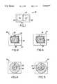
- FIG. 1is a top-view of a monolithic optical emitter-detector of the present invention where the emitter and detector are edge-coupled;
- FIGS. 2-5are cross-sectional views of monolithic optical emitter-detectors of the present invention where the emitter and detector are peripherally-coupled;
- FIGS. 6-8are cross-sectional elevation views of monolithic optical emitter-detectors of the present invention where the emitter and detector are vertically-coupled;
- FIGS. 9-16are schematic diagrams of monolithic optical emitter-detectors of the present invention where the emitter and detector are vertically-coupled.
- FIG. 17is a block diagram of an application of the monolithic optical emitter-detector of the present invention.
- the devices described hereare based in part on the technology used in the Siemens® IL300 family of aluminum gallium arsenide (AlGaAs) linear optocouplers, discussed in the Siemens Optoelectronics Data Book 1993, pp. 5-115 through 5-122, and pp. 11-177 through 11-193. It should be understood that other devices can be used. Also, the couplers could be used with other types of electromagnetic radiation, such as infrared radiation or ultraviolet light.
- AlGaAsaluminum gallium arsenide
- FIG. 1One configuration of a monolithic emitter-detector constructed in accordance with the present invention is shown in FIG. 1.
- the emitter-detector assembly 10has a two diodes, an emitter D1 12 and a detector D2 14 on a single substrate 16.
- the emitter 12 and the detector 14are adjacent or side-by-side, providing edge coupling through the substrate 16 in the region 18 shared by the two components 12 and 14.
- the LED waferis sliced in such a fashion that two diodes remain attached to one another at one edge. Insulation between the adjacent diodes can be achieved by using either mechanical or chemical deposition methods.
- the devicecan be packaged as a three-lead LED or perform as a servo-controlled emitter in a linear coupler.
- Monolithic emitter-detector devicescan also be configured such that the emitter and detector are connected by a lateral, peripheral edge, as illustrated in FIGS. 2 through 5.
- the monolithic emitter-detector 30 shownhas an emitter D1 32 that is physically surrounded by a detector D2 34.
- the emitter 32 and the detector 34are positioned on a substrate 36. Coupling occurs at a peripheral edge 38.
- the emitter 32can have any suitable shape such as round, oval, square, rectangular, curvilinear, or interdigitated.
- FIG. 3A similar monolithic emitter-detector 50 is shown in FIG. 3.
- the emitter D1 52surrounds the detector D2 54. Coupling occurs as in the device of FIG. 2 at a peripheral edge 58.
- monolithic emitter-detectors 70 and 90 having round emitters and detectorsare shown in FIGS. 4 and 5, respectively. Each has its respective emitter D1 72 or 92 and detector D2 74 or 94.
- the devices of FIGS. 2-5can be packaged as a three-lead LED or perform as a servo-controlled emitter in a linear coupler.
- FIGS. 6-8Monolithic emitter-detectors having vertically-coupled surfaces are shown in FIGS. 6-8.
- the first such device 110in FIG. 6, has a substrate 112, an emitter 114, and a detector 116.
- the detector 116can be physically or chemically grown on top of the emitter 114, the two being insulated from one another.
- the emitter 114radiates through the detector 116 or through the substrate 112 if it is sufficiently transparent.
- a second device 130is shown in FIG. 7. Similar to the device in FIG. 6, this device 130 has a substrate 132, an emitter 134, and a detector 136. A window 138 in the detector 136 is provided by physical or chemical (etching) means and allows the optical radiation from the emitter 134 to pass through.
- the device 150has a substrate 152, a detector 154, and an emitter 156.
- the emitter 156radiates upwardly, but some of its radiation also passes through the surface adjacent the detector 154, providing feedback to the detector 154 and permitting maximum coupling out of the emitter's 156 major radiating surface 158.
- FIGS. 9 through 16eight variations are illustrated.
- detectors 170are positioned above emitters 172, which in turn sit on substrates 174.
- the detectors 170sit directly on the substrates 174, and the emitters 172 are positioned above the detectors 170.
- the four circuitsdiffer in how the diodes are interconnected.
- the cathode 176 of the detector 170is connected to the anode 178 of the emitter 172, while the anode of the detector 170 of the second device (FIG. 10) is connected to the cathode of the emitter 172.
- the anodesFIG. 11
- the cathodesFIG. 12
- FIG. 17An application of the monolithic optical emitter-detector of the present invention is shown in FIG. 17.
- the circuit shownis a linear coupler of the kind discussed in the copending application referenced above.
- the couplerhas an input 200 that drives a control amplifier 202.
- the amplifier 202has a signal input 204, a feedback input 206, and an output 208.
- the signal input 204 of the amplifier 202is connected to the coupler input 200.
- the next stage of the coupleris a monolithic emitter-detector 210, which has an emitter 212, a detector 214, and a substrate 216.
- the output 208 of the control amplifier 202is provided to the emitter 212; the detector 214 provides a feedback signal 218 to the feedback input 206 of the amplifier 202.
- Optical radiation 222 generated by the emitter 212illuminates an output detector 222 that generates an output 224, providing isolation between the input 200 and the output 224.
- the detector 214is receiving optical radiation 226 from the emitter 212 to develop the feedback signal 218.
- the same circuitrycan be used to construct a constant-controllable output flux LED lamp.
- the optical radiation 220 of the emitter 212is received by a human or electronic receiver 230 as appropriate to the application.
Landscapes
- Light Receiving Elements (AREA)
Abstract
Description
Claims (6)
Priority Applications (1)
| Application Number | Priority Date | Filing Date | Title |
|---|---|---|---|
| US08/314,170US5448077A (en) | 1993-09-30 | 1994-09-28 | Monolithic optical emitter-detector having a control amplifier with a feedback signal |
Applications Claiming Priority (2)
| Application Number | Priority Date | Filing Date | Title |
|---|---|---|---|
| US12981493A | 1993-09-30 | 1993-09-30 | |
| US08/314,170US5448077A (en) | 1993-09-30 | 1994-09-28 | Monolithic optical emitter-detector having a control amplifier with a feedback signal |
Related Parent Applications (1)
| Application Number | Title | Priority Date | Filing Date |
|---|---|---|---|
| US12981493ADivision | 1993-09-30 | 1993-09-30 |
Publications (1)
| Publication Number | Publication Date |
|---|---|
| US5448077Atrue US5448077A (en) | 1995-09-05 |
Family
ID=22441723
Family Applications (1)
| Application Number | Title | Priority Date | Filing Date |
|---|---|---|---|
| US08/314,170Expired - Fee RelatedUS5448077A (en) | 1993-09-30 | 1994-09-28 | Monolithic optical emitter-detector having a control amplifier with a feedback signal |
Country Status (1)
| Country | Link |
|---|---|
| US (1) | US5448077A (en) |
Cited By (9)
| Publication number | Priority date | Publication date | Assignee | Title |
|---|---|---|---|---|
| WO1997002597A1 (en)* | 1995-06-30 | 1997-01-23 | Siemens Components, Inc. | A method of manufacturing a monolithic linear optocoupler |
| US5767997A (en)* | 1996-07-05 | 1998-06-16 | Lucent Technologies Inc. | Method and arrangement for a combined modulator/photodetector |
| US5903016A (en)* | 1995-06-30 | 1999-05-11 | Siemens Components, Inc. | Monolithic linear optocoupler |
| US6527460B2 (en)* | 2001-06-27 | 2003-03-04 | International Business Machines Corporation | Light emitter control system |
| US20050053379A1 (en)* | 1998-08-26 | 2005-03-10 | Jockerst Nan Marie | System and method for bi-directional optical communication using stacked emitters and detectors |
| US7039320B1 (en)* | 1999-11-05 | 2006-05-02 | Fsona Communications Corporation | Portable laser transceiver |
| US20110006328A1 (en)* | 2008-01-29 | 2011-01-13 | Nxp B.V. | Lighting unit with temperature compensation |
| US20140119740A1 (en)* | 2012-10-25 | 2014-05-01 | Avago Technologies General Ip (Singapore) Pte. Ltd. | Opto-Isolator With Compensation Circuit |
| US10368411B2 (en) | 2016-09-20 | 2019-07-30 | Bolb Inc. | Ultraviolet light module having output power control mechanism |
Citations (6)
| Publication number | Priority date | Publication date | Assignee | Title |
|---|---|---|---|---|
| US3582661A (en)* | 1967-09-25 | 1971-06-01 | Philips Corp | Photoelectric yarn measurer having reference channel |
| US3699407A (en)* | 1971-09-29 | 1972-10-17 | Motorola Inc | Electro-optical coupled-pair using a schottky barrier diode detector |
| US4190747A (en)* | 1978-04-05 | 1980-02-26 | Bell Telephone Laboratories, Incorporated | Signal corrected optocoupled device |
| US4221485A (en)* | 1979-06-04 | 1980-09-09 | Honeywell Inc. | Optical smoke detector |
| US4667212A (en)* | 1984-09-03 | 1987-05-19 | Kabushiki Kaisha Toshiba | Integrated optical and electric circuit device |
| US4970381A (en)* | 1989-04-28 | 1990-11-13 | At&T Bell Laboratories | Integrated optics facsimile apparatus |
- 1994
- 1994-09-28USUS08/314,170patent/US5448077A/ennot_activeExpired - Fee Related
Patent Citations (6)
| Publication number | Priority date | Publication date | Assignee | Title |
|---|---|---|---|---|
| US3582661A (en)* | 1967-09-25 | 1971-06-01 | Philips Corp | Photoelectric yarn measurer having reference channel |
| US3699407A (en)* | 1971-09-29 | 1972-10-17 | Motorola Inc | Electro-optical coupled-pair using a schottky barrier diode detector |
| US4190747A (en)* | 1978-04-05 | 1980-02-26 | Bell Telephone Laboratories, Incorporated | Signal corrected optocoupled device |
| US4221485A (en)* | 1979-06-04 | 1980-09-09 | Honeywell Inc. | Optical smoke detector |
| US4667212A (en)* | 1984-09-03 | 1987-05-19 | Kabushiki Kaisha Toshiba | Integrated optical and electric circuit device |
| US4970381A (en)* | 1989-04-28 | 1990-11-13 | At&T Bell Laboratories | Integrated optics facsimile apparatus |
Cited By (12)
| Publication number | Priority date | Publication date | Assignee | Title |
|---|---|---|---|---|
| WO1997002597A1 (en)* | 1995-06-30 | 1997-01-23 | Siemens Components, Inc. | A method of manufacturing a monolithic linear optocoupler |
| US5903016A (en)* | 1995-06-30 | 1999-05-11 | Siemens Components, Inc. | Monolithic linear optocoupler |
| CN1097850C (en)* | 1995-06-30 | 2003-01-01 | 西门子微电子公司 | Monolithic linear optocoupler fabrication method |
| US5767997A (en)* | 1996-07-05 | 1998-06-16 | Lucent Technologies Inc. | Method and arrangement for a combined modulator/photodetector |
| US20050053379A1 (en)* | 1998-08-26 | 2005-03-10 | Jockerst Nan Marie | System and method for bi-directional optical communication using stacked emitters and detectors |
| US7039320B1 (en)* | 1999-11-05 | 2006-05-02 | Fsona Communications Corporation | Portable laser transceiver |
| US6527460B2 (en)* | 2001-06-27 | 2003-03-04 | International Business Machines Corporation | Light emitter control system |
| US20110006328A1 (en)* | 2008-01-29 | 2011-01-13 | Nxp B.V. | Lighting unit with temperature compensation |
| US8174041B2 (en) | 2008-01-29 | 2012-05-08 | Nxp B.V. | Lighting unit with temperature compensation |
| US20140119740A1 (en)* | 2012-10-25 | 2014-05-01 | Avago Technologies General Ip (Singapore) Pte. Ltd. | Opto-Isolator With Compensation Circuit |
| US8983304B2 (en)* | 2012-10-25 | 2015-03-17 | Avago Technologies General Ip (Singapore) Pte. Ltd. | Opto-isolator with compensation circuit |
| US10368411B2 (en) | 2016-09-20 | 2019-07-30 | Bolb Inc. | Ultraviolet light module having output power control mechanism |
Similar Documents
| Publication | Publication Date | Title |
|---|---|---|
| US5753928A (en) | Monolithic optical emitter-detector | |
| US5753929A (en) | Multi-directional optocoupler and method of manufacture | |
| US4533833A (en) | Optically coupled integrated circuit array | |
| CA2091525C (en) | Semiconductor optical device having device regions and diffraction gratings | |
| US5146078A (en) | Articles and systems comprising optically communicating logic elements including an electro-optical logic element | |
| US6583445B1 (en) | Integrated electronic-optoelectronic devices and method of making the same | |
| US5726500A (en) | Semiconductor hybrid component | |
| US5448077A (en) | Monolithic optical emitter-detector having a control amplifier with a feedback signal | |
| US4124860A (en) | Optical coupler | |
| EP0632509B1 (en) | A linear integrated optocoupler and method for forming the same | |
| EP1033596A2 (en) | A method of and a device for coupling optical fibres and opto-electronic components | |
| US20020050561A1 (en) | Socket and a system for optoelectronic interconnection and a method of fabricating such socket and system | |
| WO1992013363A2 (en) | Light emitting diode bars and arrays and method of making same | |
| US4952791A (en) | Monolithic apparatus comprising optically interconnected quantum well devices | |
| US3414733A (en) | Annularly shaped light emitter and photocell connected by plug-in light conducting pad | |
| US6821026B2 (en) | Redundant configurable VCSEL laser array optical light source | |
| Van Drieënhuizen et al. | Optocoupler based on the avalanche light emission in silicon | |
| US4588896A (en) | Bistable circuits having a monolithic device formed with light emitting diodes and detectors | |
| WO1987004566A1 (en) | Interconnects for wafer-scale-integrated assembly | |
| JP2004501502A (en) | Method of manufacturing optical transmitting / receiving device, and optical transmitting / receiving device manufactured based on the method | |
| EP0646973B1 (en) | Linear bidirectional optocoupler | |
| Jokerst et al. | Communication through stacked silicon circuitry using integrated thin film InP-based emitters and detectors | |
| EP0222338B1 (en) | Semiconductor photo-sensing device | |
| JPH0936413A (en) | Optically coupled semiconductor device | |
| Brown et al. | Monolithically integrated 1× 12 array of planar InGaAs/InP photodiodes |
Legal Events
| Date | Code | Title | Description |
|---|---|---|---|
| AS | Assignment | Owner name:SIEMENS MICROELECTRONICS, INC., CALIFORNIA Free format text:CHANGE OF NAME;ASSIGNOR:SIEMENS COMPONENTS, INC.;REEL/FRAME:009027/0590 Effective date:19971001 | |
| FEPP | Fee payment procedure | Free format text:PAYOR NUMBER ASSIGNED (ORIGINAL EVENT CODE: ASPN); ENTITY STATUS OF PATENT OWNER: LARGE ENTITY | |
| FPAY | Fee payment | Year of fee payment:4 | |
| REMI | Maintenance fee reminder mailed | ||
| LAPS | Lapse for failure to pay maintenance fees | ||
| STCH | Information on status: patent discontinuation | Free format text:PATENT EXPIRED DUE TO NONPAYMENT OF MAINTENANCE FEES UNDER 37 CFR 1.362 | |
| FP | Lapsed due to failure to pay maintenance fee | Effective date:20030905 | |
| AS | Assignment | Owner name:INFINEON TECHNOLOGIES CORPORATION, CALIFORNIA Free format text:CHANGE OF NAME;ASSIGNOR:SIEMENS DRAM SEMICONDUCTOR CORPORATION;REEL/FRAME:014363/0078 Effective date:19990401 Owner name:INFINEON TECHNOLOGIES NORTH AMERICA CORP., CALIFOR Free format text:CHANGE OF NAME;ASSIGNOR:INFINEON TECHNOLOGIES CORPORATION;REEL/FRAME:014363/0102 Effective date:19990930 Owner name:SIEMENS DRAM SEMICONDUCTOR CORPORATION, CALIFORNIA Free format text:ASSIGNMENT OF ASSIGNORS INTEREST;ASSIGNOR:SIEMENS MICROELECTRONICS, INC.;REEL/FRAME:014363/0076 Effective date:19990330 Owner name:SIEMENS MICROELECTRONICS, INC., CALIFORNIA Free format text:CHANGE OF NAME;ASSIGNOR:SIEMENS COMPONENTS, INC.;REEL/FRAME:014363/0074 Effective date:19971007 Owner name:VISHAY INFRARED COMPONENTS, CALIFORNIA Free format text:CHANGE OF NAME;ASSIGNOR:INFINEON TECHNOLOGIES NORTH AMERICA CORP.;REEL/FRAME:014363/0081 Effective date:19990805 | |
| AS | Assignment | Owner name:VISHAY INFRARED COMPONENTS, CALIFORNIA Free format text:CORRECTIVE FROM CHANGE OF NAME TO ASSIGNMENT AND CORRECTED ADDRESS.;ASSIGNOR:INFINEON TECHNOLOGIES NORTH AMERICA CORP.;REEL/FRAME:014373/0348 Effective date:19990805 Owner name:VISHAY INFRARED COMPONENTS, CALIFORNIA Free format text:CORRECTIVE ASSIGNMENT TO CORRECT THE NATURE OF CONVEYANCE AND ASSIGNEE ADDRESS PREVIOUSLY RECORDED AT REEL 014363 FRAME 0081. THE ASSIGNOR HEREBY CONFIRMS THE ASSIGNMENT OF THE ENTIRE INTEREST;ASSIGNOR:INFINEON TECHNOLOGIES NORTH AMERICA CORP.;REEL/FRAME:014373/0348 Effective date:19990805 |