US5444737A - Wireless data transceiver - Google Patents
Wireless data transceiverDownload PDFInfo
- Publication number
- US5444737A US5444737AUS08/150,401US15040193AUS5444737AUS 5444737 AUS5444737 AUS 5444737AUS 15040193 AUS15040193 AUS 15040193AUS 5444737 AUS5444737 AUS 5444737A
- Authority
- US
- United States
- Prior art keywords
- signal
- modulated
- frequency
- recited
- receiving
- Prior art date
- Legal status (The legal status is an assumption and is not a legal conclusion. Google has not performed a legal analysis and makes no representation as to the accuracy of the status listed.)
- Expired - Lifetime
Links
Images


Classifications
- H—ELECTRICITY
- H03—ELECTRONIC CIRCUITRY
- H03C—MODULATION
- H03C3/00—Angle modulation
- H03C3/02—Details
- H03C3/09—Modifications of modulator for regulating the mean frequency
- H03C3/0908—Modifications of modulator for regulating the mean frequency using a phase locked loop
- H03C3/0975—Modifications of modulator for regulating the mean frequency using a phase locked loop applying frequency modulation in the phase locked loop at components other than the divider, the voltage controlled oscillator or the reference clock
- H—ELECTRICITY
- H04—ELECTRIC COMMUNICATION TECHNIQUE
- H04B—TRANSMISSION
- H04B1/00—Details of transmission systems, not covered by a single one of groups H04B3/00 - H04B13/00; Details of transmission systems not characterised by the medium used for transmission
- H04B1/38—Transceivers, i.e. devices in which transmitter and receiver form a structural unit and in which at least one part is used for functions of transmitting and receiving
- H04B1/40—Circuits
- H—ELECTRICITY
- H04—ELECTRIC COMMUNICATION TECHNIQUE
- H04L—TRANSMISSION OF DIGITAL INFORMATION, e.g. TELEGRAPHIC COMMUNICATION
- H04L25/00—Baseband systems
- H04L25/38—Synchronous or start-stop systems, e.g. for Baudot code
- H04L25/40—Transmitting circuits; Receiving circuits
- H04L25/49—Transmitting circuits; Receiving circuits using code conversion at the transmitter; using predistortion; using insertion of idle bits for obtaining a desired frequency spectrum; using three or more amplitude levels ; Baseband coding techniques specific to data transmission systems
- H04L25/4917—Transmitting circuits; Receiving circuits using code conversion at the transmitter; using predistortion; using insertion of idle bits for obtaining a desired frequency spectrum; using three or more amplitude levels ; Baseband coding techniques specific to data transmission systems using multilevel codes
- H04L25/4923—Transmitting circuits; Receiving circuits using code conversion at the transmitter; using predistortion; using insertion of idle bits for obtaining a desired frequency spectrum; using three or more amplitude levels ; Baseband coding techniques specific to data transmission systems using multilevel codes using ternary codes
- H04L25/4925—Transmitting circuits; Receiving circuits using code conversion at the transmitter; using predistortion; using insertion of idle bits for obtaining a desired frequency spectrum; using three or more amplitude levels ; Baseband coding techniques specific to data transmission systems using multilevel codes using ternary codes using balanced bipolar ternary codes
- H—ELECTRICITY
- H04—ELECTRIC COMMUNICATION TECHNIQUE
- H04L—TRANSMISSION OF DIGITAL INFORMATION, e.g. TELEGRAPHIC COMMUNICATION
- H04L27/00—Modulated-carrier systems
- H04L27/10—Frequency-modulated carrier systems, i.e. using frequency-shift keying
- H04L27/12—Modulator circuits; Transmitter circuits
- H—ELECTRICITY
- H04—ELECTRIC COMMUNICATION TECHNIQUE
- H04L—TRANSMISSION OF DIGITAL INFORMATION, e.g. TELEGRAPHIC COMMUNICATION
- H04L27/00—Modulated-carrier systems
- H04L27/10—Frequency-modulated carrier systems, i.e. using frequency-shift keying
- H04L27/14—Demodulator circuits; Receiver circuits
- H04L27/144—Demodulator circuits; Receiver circuits with demodulation using spectral properties of the received signal, e.g. by using frequency selective- or frequency sensitive elements
- H04L27/148—Demodulator circuits; Receiver circuits with demodulation using spectral properties of the received signal, e.g. by using frequency selective- or frequency sensitive elements using filters, including PLL-type filters
Definitions
- the present inventionrelates to wireless data transceivers, and in particular, to asynchronous, full duplex wireless data MODEMs with data encoding and decoding.
- a common conventional communication linkhas been a data transceiver often referred to as a MODEM (MODulator/DEModulator) in which data is modulated, transmitted over the communication medium, and then demodulated at the receiving end.
- MODEMMODulator/DEModulator
- MODEMsPerhaps one of the most common MODEMs is one in which the data is transmitted and received over telephone lines. These types of MODEMs, as well as many other types, rely on a "hard-wired" connection and typically operate in a simplex or half duplex mode. However, hard-wired communication links tend to restrict the mobility of the users. Further, any reconfiguration of the communication link requires the time and expense of relocating, or otherwise reconfiguring, the hard-wired connections, e.g. installing and/or relocating cables.
- wireless MODEMsSuch MODEMs continue to transmit and receive data but do so without using wires or cabling as the communication medium. Instead, data transmission is accomplished wirelessly, i.e. "over-the-air", with the atmosphere (or space) as the communication medium. This results in a significant increase in mobility of the users, as well as enhanced opportunities to operate in a full duplex communication mode.
- a data transceiver in accordance with a preferred embodiment of the present inventionuses separate transmit and receiver antennas for transmitting and receiving data-modulated signals, respectively.
- a single local oscillatorprovides both the RF carrier for the transmit signal and the local oscillator ("LO") signal for the down-conversion of the receive signal in the receiver section.
- the LO signalis conveyed from the transmitter section to the receiver section in the form of the radiated transmit signal from the transmit antenna to the receive antenna.
- Full duplex operationis achieved by cancelling out the transmit data from the down-converted receive signal which has been introduced by the modulated transmit signal used as the LO signal, and by setting the carrier of the local oscillator at a frequency which is offset from that of the incoming data-modulated carrier signal by an amount equal to the desired intermediate frequency.
- a data transceiver in accordance with an alternative preferred embodiment of the present inventionuses a single antenna for transmitting and receiving the modulated signals. Conveyance of the LO signal from the transmitter section to the receiver section is effected by coupling a portion of the transmit signal which is intended to be radiated from the antenna into the receiver via a signal coupler.
- a frequency modulatorin which a phase-lock-loop is used for generating a frequency-modulated signal.
- the phase-lock-loopreceives a reference signal and generates an output signal which is synchronized to the reference signal in accordance with an internally generated frequency control signal.
- a modulatorreceives a binary data signal and in accordance therewith modulates the frequency control signal, which in turn causes the output signal frequency to be modulated.
- a binary-to-trinary data encoderfor encoding binary data to trinary data.
- the first of the three trinary data valuescorresponds to an absence of binary data transitions
- the second of the three trinary data valuescorresponds to positive binary data transitions
- the third of the three trinary data valuescorresponds to negative binary data transitions.
- the trinary data valuesare represented by a frequency-modulated signal in which one of three frequencies each represents one of the trinary data values.
- a trinary-to-binary data decoderreceives and demodulates a trinary modulated signal to produce a demodulated trinary signal containing trinary data.
- a decoderdecodes the demodulated trinary signal to a binary signal which contains binary data corresponding to the trinary data.
- the demodulatoris a frequency demodulator and the trinary modulated signal is a frequency-modulated signal.
- FIG. 1is a functional block diagram of two data transceivers in accordance with a preferred embodiment of the present invention.
- FIG. 2is a functional block diagram of a data transceiver in accordance with the present invention.
- FIG. 3illustrates exemplary signal waveforms for various signals within the data transceiver of FIG. 2.
- FIG. 4illustrates exemplary frequency spectrums for the transmit and receive signals of the data transceiver of FIG. 2.
- FIGS. 5A1-5A2, 5B and 5C togetherare a schematic diagram of a preferred embodiment of the data transceiver of FIG. 2.
- FIGS. 6A and 6Bare functional block diagrams of data transceivers in accordance with an alternative preferred embodiment of the present invention.
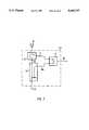
- FIG. 7illustrates an exemplary signal coupler for the data transceivers of FIG. 6A.
- a communication system 10 using two data transceivers 12, 14 in accordance with a preferred embodiment of the present inventionincludes two each of the following elements: modulator 16; frequency modulator-transmitter 18; transmitter antenna 20; receiver antenna 22; mixer 24; and IF amplifier and demodulator 26 (all connected substantially as shown).
- modulator 16 and frequency modulator-transmitter 18constitute the transmitter section
- mixer 24 and IF amplifier and demodulator 26constitute the receiver section.
- the discussion that followsis addressed specifically to the first transceiver 12, but it should be understood that the second transceiver 14 operates in a similar fashion, with the exception of its transmit and receive frequencies as discussed further below.
- the modulator 16receives binary transmit data 28 as its input modulation signal, and in accordance therewith provides a modulation signal 30 to the modulator-transmitter 18.
- the modulator 16also provides a modulation feedback signal 32 to the IF amplifier and demodulator 26 in the receiver for use in cancellation of the transmit data from the demodulated receive signal (discussed further below).
- the modulator-transmitter 18outputs a modulated RF signal 34 (with carrier frequency F1), modulated by its input modulation signal 30, to the transmitter antenna 20.
- a modulated RF signal 34(with carrier frequency F1), modulated by its input modulation signal 30, to the transmitter antenna 20.
- One component 36a of the radiated transmit signalis received by the second transceiver 14, and another component 36b is received by the receiver antenna 22 of the subject transceiver 12 for use as its receiver LO signal (discussed further below).
- the receiver antenna 22receives a modulated RF signal 36c from the second transceiver 14 and the transmitted modulated RF signal 36b from its companion transmitter.
- the resulting combined signal 38is received by the mixer 24 which mixes the two signal components to produce an IF signal 40.
- the IF amplifier and demodulator 26receives the IF signal 40, demodulates it and outputs the resulting receive binary data 42. As discussed further below, this demodulation uses a modulation feedback signal 32 to cancel out the effects of the modulation of the transmit signal 36b used as the local oscillator in the receiver.
- Full duplex operation of the two transceivers 12, 14is achieved by offsetting their respective transmit carrier frequencies F1 and F2 by that amount desired to be used as the IF frequency F3.
- Full duplex operationis enhanced by using a modulation feedback signal 32 representing the transmitter modulation to cancel out modulation effects within the receiver IF signal 40 due to the use of the transmitted modulated RF signal 36b as the receiver local oscillator.
- An advantage of the circuit topology of FIG. 1is the lack of a requirement for a hard-wired RF interface between the receiver and transmitter, even though only a single local oscillator is used. In other words, even though the sole local oscillator is resident within the transmitter, it need not be hard-wired to the receiver to provide a LO signal thereto, since the LO signal for the receiver is supplied via the transmitter and receiver antennas 20, 22 as the transmit signal 36b. Hence, a much lower frequency interface is all that is needed, i.e. to provide the modulation feedback signal 32.
- the transmitternamely the modulator 16 and frequency modulator-transmitter 18, is constructed from a phase-lock-loop ("PLL") 44 which includes: voltage-controlled oscillator (“VCO”) 46; divide-by-N prescaler 48; frequency reference source 50; phase comparator 52; lowpass loop filter 54; and signal summer 56 (all connected substantially as shown).
- VCOvoltage-controlled oscillator
- divide-by-N prescaler 48frequency reference source 50
- phase comparator 52phase comparator 52
- lowpass loop filter 54lowpass loop filter 54
- signal summer 56all connected substantially as shown.
- the VCO 46produces a RF output signal 34 which is received by the prescaler 48.
- the prescaled signal 58is received by the phase comparator 52, along with a reference signal 60 from the frequency reference source 50.
- the phase comparator 52compares the relative phases of the prescaled 58 and reference 60 signals and produces an error signal 62 representing the difference between those signal phases.
- the signal summer 56receives the error signal 62 and sums it with the transmit data 28.
- the sum signal 64is lowpass filtered by the loop filter 54 to produce the frequency control signal 66 for the VCO 46.
- the sum signal 64is the same as the error signal 62.
- the PLL 44is in a synchronized state, meaning that the phase of the VCO 46 output 34 is synchronized, or locked, with that of the reference signal 60.
- the sum signal 64, and therefore the VCO frequency control signal 66become modulated by the transmit data 28, thereby causing the RF output signal 34 of the VCO 46 to be frequency-modulated. It is this RF signal 34 (which is frequency-modulated) that is transmitted via the transmitter antenna 20.
- the filtered sum signal 66is conveyed as the modulation feedback signal 32 to the receiver section.
- the receiverhas a receiver antenna 22 and mixer 24.
- the IF amplifier and demodulator 26is made up of a serial combination of: bandpass filter 68; IF amplifier 70; frequency discriminator 72; signal summer 74; bandpass filter 76; and amplitude window discriminator 78 (all connected substantially as shown).
- the receive signal 36c from the other data transceiver 14is received by the receiver antenna 22, as is the transmitted signal 36b from the companion transmitter. As discussed above, the combined signals 38 are received and mixed within the mixer 24 to produce the IF signal 40.
- a bandpass filter 68filters the IF signal to reduce incoming signal noise and spurious signals.
- the filtered signal 80is amplified by the IF amplifier 70.
- the IF amplifier 70produces an amplified IF signal 82 which goes to the frequency discriminator 72 for demodulation thereof in the form of frequency discrimination.
- the IF amplifier 70also produces a DC signal which is proportional to the logarithm of the input signal 80 to the IF amplifier 70 and thereby represents the signal strength of that signal 70. Accordingly, this DC signal 84 is commonly referred to as a “receive signal strength indicator” (“RSSI”) signal.
- RSSIreceive signal strength indicator
- the demodulated signal 86is summed differentially within the signal summer 74 with the transmit data modulation feedback signal 32. This causes the effects of the transmit data within the demodulated signal 86 to be netted, e.g. subtracted, out.
- the resulting difference signal 88is filtered once again by a bandpass filter 76. This filtered signal 90 goes to the amplitude window discriminator 78, along with the RSSI signal 84 from the IF amplifier 70 (discussed above).
- the filtered, demodulated signal 90is amplitude window-discriminated, i.e. compared in amplitude against two amplitude thresholds, within the amplitude window discriminator 78 to decode the trinary data back to binary data (discussed further below).
- the RSSI signal 84 from the IF amplifier 70is used to enable the amplitude window discriminator 78 (discussed further below).
- the decoded, i.e. binary, dataconstitutes the outputted receive data 42.
- the frequency modulation of the VCO 46 output 34 and the demodulation and decoding of the receive datacan be better understood.
- the transmit data 28 and receive data 42are binary in form; however, in between, the data is trinary in form.
- the binary transmit data 28is encoded to trinary data which is used to modulate the transmit signal 34 produced by the VCO 46 in the PLL 44.
- the receive signal 36cis frequency modulated with trinary data representing binary data.
- the demodulated and filtered signal 90also represents trinary data corresponding to the original binary transmit data 28. The decoding of this trinary data back to binary takes place within the amplitude window discriminator 78.
- FIG. 3Ashows a single positive data transition of the transmit data 28.
- This step input to the signal summer 56(FIG. 2) produces a positive-going transient in the sum signal 64 which is filtered by the loop filter 54.
- This positive transient in the VCO frequency control signal 66causes the frequency of the VCO output signal 34 to increase accordingly.
- the inverseis true, meaning that negative data transitions in the transmit data 28 produce negative transients in the VCO frequency control signal 66 and frequency of the output signal 34.
- the PLL 44compensates for such output frequency transients (by appropriately adjusting the phase error signal 62), and the VCO frequency control signal 66 returns to its steady-state level.
- the duration of the transient depicted in FIG. 3Bis approximately 8 microseconds.
- a binary transmit data stream 28produces a VCO frequency control signal 66 with positive and negative transients as shown.
- Those portions of the VCO frequency control signal 66 waveform labeled Acorrespond to the steady-state conditions after the PLL 44 has compensated for any transients induced by any positive or negative transmit data 28 transitions.
- Those portions labeled Bare the positive transient peaks resulting from positive binary data transitions in the transmit data 28, and those portions labeled C are the negative transient peaks resulting from negative binary data transitions in the transmit data 28.
- FIGS. 3C and 3Dare also applicable when considering the demodulation and decoding of the receive signal by the receiver.
- FIG. 3Drepresents the filtered, demodulated signal 90 (trinary data) inputted to the amplitude window discriminator 78 (FIG. 2).
- the amplitude window discriminator 78with internally set high TH and low TL thresholds (and enabled by the RSSI signal 84), decodes the trinary input data 90 into two intermediate data signals 42a and 42b, as shown in FIGS. 3E and 3F, respectively.
- the first intermediate data signal 42ais a "positive edge signal".
- This signal 42ais a binary signal whose trailing edges, i.e. negative transitions, occur at those points at which the trinary data 90 rises above the high threshold TH, and whose leading edges, i.e. positive transitions, occur at those points at which the trinary data 90 falls below the high threshold TH.
- the second intermediate data signal 42bis a "negative edge signal".
- This signal 42bis a binary signal whose trailing edges, i.e. negative transitions, occur at those points at which the trinary data 90 crosses below the low threshold TL, and whose leading edges, i.e. positive transitions, occur at those points at which the trinary data 90 rises above the low threshold TL.
- the output frequency spectrum of the transmit signal 34(and receive signal 36c) can be better understood.
- the output frequencyincreases to an upper "peak" frequency f +P .
- the output frequencydecreases to a lower "peak" frequency f -P .
- the trinary dataas represented by the VCO frequency control signal 66, produces a frequency-modulated output signal 34.
- the VCO 46is a self-excited oscillator which includes transistor Q1 and a printed antenna element 20 (e.g. microstrip).
- the phase comparator 52is an EXCLUSIVE-OR phase comparator U2B.
- the divide-by-N prescaler 48is a divide-by-256/257 prescaler U7 (whose divide ratio is selectable with switch S1 to be either 256 or 257), the output of which is amplified and level-converted with two EXCLUSIVE-OR gates U2D and U2C connected as inverters.
- the final EXCLUSIVE-OR gate U2Aalso connected as an inverter, operates with crystal Y1 (approximately 3.58 megahertz [MHz]) as a crystal oscillator for the frequency reference source 50.
- the gain and frequency response of the PLL 44are set, using the components and values as shown, so that a step input to the loop produces the transient response shown in FIG. 3B.
- signals from the receive antenna 22are matched to the mixer 24 with a resonant transmission line (e.g. microstrip).
- the mixer 24uses a pair of Schottky diodes D1 connected in a single-balanced configuration to produce a balanced IF signal 40.
- the bandpass filter FL1 68is a two-pole L-C filter (e.g. TOKO H354BAI-1425-DAD), and performs a balanced-to-unbalanced signal conversion, as well as provide selectivity at the IF frequency of approximately 3.5 MHz.
- the IF amplifier 70 and frequency discriminator 72are embodied within integrated circuit U6 (Signetics NE604). Additional IF filtering is provided by filter FL2 (e.g. TOKO H354BAI-1425-DAD), and elements C14, L1 and R8 form a quadrature network for use in the frequency discrimination performed by U6. Noninverted and inverted discriminator outputs 86a, 86b are available (discussed further below) using switch S2. The selected output 86 is summed with the modulation feedback signal 32 (which is inverted, amplified and phase-compensated with amplifier U5A with a phase delay to compensate for the receiver front-end phase delays), and then filtered in an active lowpass filter U5B.
- filter FL2e.g. TOKO H354BAI-1425-DAD
- elements C14, L1 and R8form a quadrature network for use in the frequency discrimination performed by U6.
- Noninverted and inverted discriminator outputs 86a, 86bare
- the RSSI signal 84is used to activate the window discriminator 78. This activation is achieved by using the output of voltage comparator U1D to selectively provide a current path to ground for the voltage divider R15, R13, R17 which provides the reference voltages for voltage comparators U1A and U1B.
- the action of the window discriminator 78is to generate pulses for positive- and negative-going transitions in the original data stream as represented by the filtered, demodulated signal 90.
- the original datais then derived from a set-reset flip-flop U3A.
- Switches S1 and S2are used to establish the compatibility of a pair of data transceivers 12, 14 (FIG. 1) in accordance with the present invention.
- the transmitter frequency reference and the receiver IFare each approximately 3.58 MHz.
- the upper and lower peak frequenciesare f C +3.58 MHz and f C -3.58 MHz, respectively.
- the transmit carrier f Cis approximately 916.48 MHz
- switch S1 set to establish the divide ratio N of U7 at 257the transmit carrier f C is approximately 920.06 MHz.
- the first data transceiver 12will receive and process the signals 36c centered about 920.06 MHz from the second data transceiver 14, and the second data transceiver 14 will receive and process the signals 36a centered about 916.48 MHz from the first data transceiver 12. This allows the data transceivers 12, 14 to operate without interfering with one another and with no self-jamming.
- switch S2 of the first data transceiver 12must be set so that the noninverted output 86a of the frequency discriminator 72 (U6 in FIG. 5) is selected, and switch S2 of the second data transceiver 14 must be set so that the inverted output 86b of the frequency discriminator 72 is selected. This ensures that the demodulated signals 90 processed by the amplitude window discriminators 78 of the data transceivers 12, 14 have the proper polarity.
- a communication system 10a using two data transceivers 12a, 14a in accordance with an alternative preferred embodiment of the present inventionincludes the same elements as shown in FIG. 1, except for the addition of a signal coupler 21a and deletion of one antenna 20. (The transmitter and receiver sections in this embodiment operate as discussed above.) A single antenna 22 is shared by the transmitter and receiver sections and the receiver LO signal is provided by the transmitter to the receiver via the signal coupler 21a.
- one form of signal coupler which can be usedis a resistive attenuator 21b.
- resistive attenuatorsare well known in the art and can be used to couple the desired amount of the RF output signal 34 into the receiver section (i.e. for use as the receiver LO signal), while still providing sufficient RF output signal 34 power to the antenna 22 for effective transmission thereof.
- an exemplary signal coupler 21acan include a directional coupler 23, circulator 25 and signal combiner 27, connected substantially as shown.
- the directional coupler 23receives the RF output signal 34 and conveys a majority 29 thereof (with respect to signal power) to the circulator 25 for routing to the antenna 22 for transmission.
- the directional coupler 23couples a minority 36e (with respect to signal power) of the RF output signal 34 to the signal combiner 27, which combines (e.g. sums) it with the incoming RF signal 31 routed from the antenna 22 by the circulator 25 to produce the combined signal 38 for the mixer 24 in the receiver section (discussed above).
Landscapes
- Engineering & Computer Science (AREA)
- Computer Networks & Wireless Communication (AREA)
- Signal Processing (AREA)
- Physics & Mathematics (AREA)
- Spectroscopy & Molecular Physics (AREA)
- Transceivers (AREA)
- Digital Transmission Methods That Use Modulated Carrier Waves (AREA)
- Dc Digital Transmission (AREA)
Abstract
Description
Claims (28)
Priority Applications (6)
| Application Number | Priority Date | Filing Date | Title |
|---|---|---|---|
| US08/150,401US5444737A (en) | 1993-05-05 | 1993-11-10 | Wireless data transceiver |
| JP6524548AJPH08510368A (en) | 1993-05-05 | 1994-04-28 | Wireless data transceiver |
| KR1019950704901AKR100291693B1 (en) | 1993-05-05 | 1994-04-28 | Wireless Data Transceiver |
| EP94915937AEP0697155B1 (en) | 1993-05-05 | 1994-04-28 | Wireless data transceiver |
| DE69411729TDE69411729T2 (en) | 1993-05-05 | 1994-04-28 | Wireless data transceiver |
| PCT/US1994/004698WO1994026049A2 (en) | 1993-05-05 | 1994-04-28 | Wireless data transceiver |
Applications Claiming Priority (2)
| Application Number | Priority Date | Filing Date | Title |
|---|---|---|---|
| US5762193A | 1993-05-05 | 1993-05-05 | |
| US08/150,401US5444737A (en) | 1993-05-05 | 1993-11-10 | Wireless data transceiver |
Related Parent Applications (1)
| Application Number | Title | Priority Date | Filing Date |
|---|---|---|---|
| US5762193AContinuation-In-Part | 1993-05-05 | 1993-05-05 |
Publications (1)
| Publication Number | Publication Date |
|---|---|
| US5444737Atrue US5444737A (en) | 1995-08-22 |
Family
ID=26736717
Family Applications (1)
| Application Number | Title | Priority Date | Filing Date |
|---|---|---|---|
| US08/150,401Expired - LifetimeUS5444737A (en) | 1993-05-05 | 1993-11-10 | Wireless data transceiver |
Country Status (6)
| Country | Link |
|---|---|
| US (1) | US5444737A (en) |
| EP (1) | EP0697155B1 (en) |
| JP (1) | JPH08510368A (en) |
| KR (1) | KR100291693B1 (en) |
| DE (1) | DE69411729T2 (en) |
| WO (1) | WO1994026049A2 (en) |
Cited By (22)
| Publication number | Priority date | Publication date | Assignee | Title |
|---|---|---|---|---|
| US5619531A (en)* | 1994-11-14 | 1997-04-08 | Research In Motion Limited | Wireless radio modem with minimal interdevice RF interference |
| US20030118187A1 (en)* | 1995-05-17 | 2003-06-26 | The Chamberlain Group, Inc. | Rolling code security system |
| US6636171B2 (en)* | 2001-01-16 | 2003-10-21 | Chen-Ping Chang | Automobile bi-direction remote control transmission circuitry |
| WO2004006455A1 (en)* | 2002-07-03 | 2004-01-15 | The Directv Group, Inc. | Method and apparatus for layered modulation |
| EP1042871A4 (en)* | 1997-10-14 | 2004-04-21 | Cypress Semiconductor Corp | Digital radio-frequency transceiver |
| US6735181B1 (en) | 2000-06-26 | 2004-05-11 | Atmel Corporation | Wireless transceiver with subtractive filter compensating both transmit and receive artifacts |
| US6839548B1 (en) | 1996-03-01 | 2005-01-04 | International Business Machines Corporation | Radio transmitter |
| US20050070238A1 (en)* | 2003-09-25 | 2005-03-31 | Texas Instruments Incorporated | Method and apparatus for reducing leakage in a direct conversion transmitter |
| US20060131420A1 (en)* | 1990-05-25 | 2006-06-22 | Koenck Steven E | Multi-level hierarchical radio-frequency communication system |
| US20070135157A1 (en)* | 2005-12-09 | 2007-06-14 | Yien-Chung Kuo | Wireless signal transceiver unit with turning mechanism for adjusting antenna direction thereof |
| US7412056B2 (en) | 1995-05-17 | 2008-08-12 | The Chamberlain Group, Inc. | Rolling code security system |
| US20080297370A1 (en)* | 1995-05-17 | 2008-12-04 | The Chamberlain Group, Inc. | Rolling code security system |
| US7492898B2 (en) | 1995-05-17 | 2009-02-17 | The Chamberlain Group, Inc. | Rolling code security system |
| WO2010014988A1 (en)* | 2008-08-01 | 2010-02-04 | Qualcomm Incorporated | Full-duplex wireless transceiver design |
| US9667286B1 (en)* | 2016-11-10 | 2017-05-30 | GM Global Technology Operations LLC | Receiver adjacent channel overload projection |
| US10652743B2 (en) | 2017-12-21 | 2020-05-12 | The Chamberlain Group, Inc. | Security system for a moveable barrier operator |
| US10862924B2 (en) | 2005-06-30 | 2020-12-08 | The Chamberlain Group, Inc. | Method and apparatus to facilitate message transmission and reception using different transmission characteristics |
| US10944559B2 (en) | 2005-01-27 | 2021-03-09 | The Chamberlain Group, Inc. | Transmission of data including conversion of ternary data to binary data |
| US10997810B2 (en) | 2019-05-16 | 2021-05-04 | The Chamberlain Group, Inc. | In-vehicle transmitter training |
| US11074773B1 (en) | 2018-06-27 | 2021-07-27 | The Chamberlain Group, Inc. | Network-based control of movable barrier operators for autonomous vehicles |
| US11423717B2 (en) | 2018-08-01 | 2022-08-23 | The Chamberlain Group Llc | Movable barrier operator and transmitter pairing over a network |
| US12149618B2 (en) | 2005-01-27 | 2024-11-19 | The Chamberlain Group Llc | Method and apparatus to facilitate transmission of an encrypted rolling code |
Citations (30)
| Publication number | Priority date | Publication date | Assignee | Title |
|---|---|---|---|---|
| US3162724A (en)* | 1961-07-03 | 1964-12-22 | Otmar E Ringelhaan | System for transmission of binary information at twice the normal rate |
| US3167712A (en)* | 1961-03-17 | 1965-01-26 | Itt | Frequency shift keyer with automatic frequency control |
| US3230310A (en)* | 1962-11-08 | 1966-01-18 | Jr Albert P Brogle | Biternary pulse code system |
| GB1122801A (en)* | 1964-05-19 | 1968-08-07 | Serck Controls Ltd | Improvements in or relating to the transmission of pulse coded information |
| US3495032A (en)* | 1968-10-07 | 1970-02-10 | Graphic Transmission Systems I | Bandwidth reduction system |
| US3631463A (en)* | 1969-03-10 | 1971-12-28 | Sperry Rand Corp | Self-clocked encoding scheme |
| US3723880A (en)* | 1970-02-12 | 1973-03-27 | Philips Corp | System for the transmission of multilevel data signals |
| US4063235A (en)* | 1975-10-31 | 1977-12-13 | Siemens Aktiengesellschaft | Non-return to zero mark to non-return to zero level code converter |
| US4087642A (en)* | 1974-05-07 | 1978-05-02 | International Standard Electric Corporation | Digital data communication system |
| US4282601A (en)* | 1979-03-02 | 1981-08-04 | Burroughs Corporation | Three level data transmission system having means for seeking a constant average value for the transmitted signals |
| US4361904A (en)* | 1979-07-31 | 1982-11-30 | Nissan Motor Company, Limited | Method of testing transceiver and transceiver including testing apparatus |
| US4397042A (en)* | 1981-07-22 | 1983-08-02 | Sumitomo Electric Industries, Ltd. | Optical modulation/demodulation system |
| US4411005A (en)* | 1981-12-21 | 1983-10-18 | General Electric Company | Data circuit for frequency modulating an oscillator |
| GB2122456A (en)* | 1982-05-19 | 1984-01-11 | Ronald R White | Method of an apparatus for duplex communications |
| US4618941A (en)* | 1983-09-19 | 1986-10-21 | Motorola, Inc. | Apparatus and method for generating filtered multilevel data from NRZ data |
| US4665531A (en)* | 1985-10-01 | 1987-05-12 | Northern Telecom Limited | Alternate mark inversion (AMI) receiver |
| US4759078A (en)* | 1986-11-14 | 1988-07-19 | Rose Communication Systems, Inc. | Coordinated local oscillator receiving system |
| WO1991012672A1 (en)* | 1990-02-09 | 1991-08-22 | Rose Communications, Inc. | Method and apparatus for selective sideband in a proximal cable-less communication system signal |
| US5095497A (en)* | 1989-10-02 | 1992-03-10 | At & T Bell Laboratories | Technique for achieving the full coding gain of encoded digital signals |
| US5101505A (en)* | 1990-02-09 | 1992-03-31 | Rose Communications, Inc. | Method and apparatus for selective sideband signal correction in a proximal cable-less communication system |
| US5107520A (en)* | 1989-01-24 | 1992-04-21 | U.S. Philips Corporation | Adaptive predistortion circuit for a digital transmission system |
| US5109545A (en)* | 1990-02-09 | 1992-04-28 | Rose Communications, Inc. | Proximal cable-less communication system with intentional signal path |
| US5119402A (en)* | 1990-06-26 | 1992-06-02 | Digital Equipment Corporation | Method and apparatus for transmission of local area network signals over unshielded twisted pairs |
| US5148448A (en)* | 1989-03-14 | 1992-09-15 | U.S. Philips Corporation | Adaptive predistortion circuit with memory |
| US5166956A (en)* | 1990-05-21 | 1992-11-24 | North American Philips Corporation | Data transmission system and apparatus providing multi-level differential signal transmission |
| US5259007A (en)* | 1991-06-19 | 1993-11-02 | Sony Corporation | Phase locked loop frequency synthesizer |
| US5303265A (en)* | 1990-06-29 | 1994-04-12 | Digital Equipment Corporation | Frequency independent encoding technique and apparatus for digital communications |
| US5313173A (en)* | 1993-04-26 | 1994-05-17 | Ericsson Ge Mobile Communications Inc. | Quadrature modulated phase-locked loop |
| US5323125A (en)* | 1993-03-15 | 1994-06-21 | Motorola, Inc. | Frequency agile method for transmitting multi-level data |
| US5355513A (en)* | 1989-12-29 | 1994-10-11 | Schlumberger Industries Limited | Transponder with reply frequency derived from frequency of received interrogation signal |
- 1993
- 1993-11-10USUS08/150,401patent/US5444737A/ennot_activeExpired - Lifetime
- 1994
- 1994-04-28DEDE69411729Tpatent/DE69411729T2/ennot_activeExpired - Fee Related
- 1994-04-28WOPCT/US1994/004698patent/WO1994026049A2/enactiveIP Right Grant
- 1994-04-28JPJP6524548Apatent/JPH08510368A/enactivePending
- 1994-04-28EPEP94915937Apatent/EP0697155B1/ennot_activeExpired - Lifetime
- 1994-04-28KRKR1019950704901Apatent/KR100291693B1/ennot_activeExpired - Fee Related
Patent Citations (30)
| Publication number | Priority date | Publication date | Assignee | Title |
|---|---|---|---|---|
| US3167712A (en)* | 1961-03-17 | 1965-01-26 | Itt | Frequency shift keyer with automatic frequency control |
| US3162724A (en)* | 1961-07-03 | 1964-12-22 | Otmar E Ringelhaan | System for transmission of binary information at twice the normal rate |
| US3230310A (en)* | 1962-11-08 | 1966-01-18 | Jr Albert P Brogle | Biternary pulse code system |
| GB1122801A (en)* | 1964-05-19 | 1968-08-07 | Serck Controls Ltd | Improvements in or relating to the transmission of pulse coded information |
| US3495032A (en)* | 1968-10-07 | 1970-02-10 | Graphic Transmission Systems I | Bandwidth reduction system |
| US3631463A (en)* | 1969-03-10 | 1971-12-28 | Sperry Rand Corp | Self-clocked encoding scheme |
| US3723880A (en)* | 1970-02-12 | 1973-03-27 | Philips Corp | System for the transmission of multilevel data signals |
| US4087642A (en)* | 1974-05-07 | 1978-05-02 | International Standard Electric Corporation | Digital data communication system |
| US4063235A (en)* | 1975-10-31 | 1977-12-13 | Siemens Aktiengesellschaft | Non-return to zero mark to non-return to zero level code converter |
| US4282601A (en)* | 1979-03-02 | 1981-08-04 | Burroughs Corporation | Three level data transmission system having means for seeking a constant average value for the transmitted signals |
| US4361904A (en)* | 1979-07-31 | 1982-11-30 | Nissan Motor Company, Limited | Method of testing transceiver and transceiver including testing apparatus |
| US4397042A (en)* | 1981-07-22 | 1983-08-02 | Sumitomo Electric Industries, Ltd. | Optical modulation/demodulation system |
| US4411005A (en)* | 1981-12-21 | 1983-10-18 | General Electric Company | Data circuit for frequency modulating an oscillator |
| GB2122456A (en)* | 1982-05-19 | 1984-01-11 | Ronald R White | Method of an apparatus for duplex communications |
| US4618941A (en)* | 1983-09-19 | 1986-10-21 | Motorola, Inc. | Apparatus and method for generating filtered multilevel data from NRZ data |
| US4665531A (en)* | 1985-10-01 | 1987-05-12 | Northern Telecom Limited | Alternate mark inversion (AMI) receiver |
| US4759078A (en)* | 1986-11-14 | 1988-07-19 | Rose Communication Systems, Inc. | Coordinated local oscillator receiving system |
| US5107520A (en)* | 1989-01-24 | 1992-04-21 | U.S. Philips Corporation | Adaptive predistortion circuit for a digital transmission system |
| US5148448A (en)* | 1989-03-14 | 1992-09-15 | U.S. Philips Corporation | Adaptive predistortion circuit with memory |
| US5095497A (en)* | 1989-10-02 | 1992-03-10 | At & T Bell Laboratories | Technique for achieving the full coding gain of encoded digital signals |
| US5355513A (en)* | 1989-12-29 | 1994-10-11 | Schlumberger Industries Limited | Transponder with reply frequency derived from frequency of received interrogation signal |
| US5109545A (en)* | 1990-02-09 | 1992-04-28 | Rose Communications, Inc. | Proximal cable-less communication system with intentional signal path |
| US5101505A (en)* | 1990-02-09 | 1992-03-31 | Rose Communications, Inc. | Method and apparatus for selective sideband signal correction in a proximal cable-less communication system |
| WO1991012672A1 (en)* | 1990-02-09 | 1991-08-22 | Rose Communications, Inc. | Method and apparatus for selective sideband in a proximal cable-less communication system signal |
| US5166956A (en)* | 1990-05-21 | 1992-11-24 | North American Philips Corporation | Data transmission system and apparatus providing multi-level differential signal transmission |
| US5119402A (en)* | 1990-06-26 | 1992-06-02 | Digital Equipment Corporation | Method and apparatus for transmission of local area network signals over unshielded twisted pairs |
| US5303265A (en)* | 1990-06-29 | 1994-04-12 | Digital Equipment Corporation | Frequency independent encoding technique and apparatus for digital communications |
| US5259007A (en)* | 1991-06-19 | 1993-11-02 | Sony Corporation | Phase locked loop frequency synthesizer |
| US5323125A (en)* | 1993-03-15 | 1994-06-21 | Motorola, Inc. | Frequency agile method for transmitting multi-level data |
| US5313173A (en)* | 1993-04-26 | 1994-05-17 | Ericsson Ge Mobile Communications Inc. | Quadrature modulated phase-locked loop |
Cited By (42)
| Publication number | Priority date | Publication date | Assignee | Title |
|---|---|---|---|---|
| US20060131420A1 (en)* | 1990-05-25 | 2006-06-22 | Koenck Steven E | Multi-level hierarchical radio-frequency communication system |
| US5727020A (en)* | 1994-11-14 | 1998-03-10 | Research In Motion Limited | Wireless radio modem with minimal interdevice RF interference |
| US5917854A (en)* | 1994-11-14 | 1999-06-29 | Research In Motion Limited | Wireless radio modem with minimal interdevice RF interference |
| US5619531A (en)* | 1994-11-14 | 1997-04-08 | Research In Motion Limited | Wireless radio modem with minimal interdevice RF interference |
| US7623663B2 (en) | 1995-05-17 | 2009-11-24 | The Chamberlain Group, Inc. | Rolling code security system |
| US20030118187A1 (en)* | 1995-05-17 | 2003-06-26 | The Chamberlain Group, Inc. | Rolling code security system |
| US8633797B2 (en) | 1995-05-17 | 2014-01-21 | The Chamberlain Group, Inc. | Rolling code security system |
| US8284021B2 (en) | 1995-05-17 | 2012-10-09 | The Chamberlain Group, Inc. | Rolling code security system |
| US8233625B2 (en) | 1995-05-17 | 2012-07-31 | The Chamberlain Group, Inc. | Rolling code security system |
| US8194856B2 (en) | 1995-05-17 | 2012-06-05 | The Chamberlain Group, Inc. | Rolling code security system |
| US7492905B2 (en) | 1995-05-17 | 2009-02-17 | The Chamberlain Group, Inc. | Rolling code security system |
| US7492898B2 (en) | 1995-05-17 | 2009-02-17 | The Chamberlain Group, Inc. | Rolling code security system |
| US7412056B2 (en) | 1995-05-17 | 2008-08-12 | The Chamberlain Group, Inc. | Rolling code security system |
| US20080297370A1 (en)* | 1995-05-17 | 2008-12-04 | The Chamberlain Group, Inc. | Rolling code security system |
| US20090016530A1 (en)* | 1995-05-17 | 2009-01-15 | The Chamberlain Group, Inc. | Rolling code security system |
| US6839548B1 (en) | 1996-03-01 | 2005-01-04 | International Business Machines Corporation | Radio transmitter |
| EP1042871A4 (en)* | 1997-10-14 | 2004-04-21 | Cypress Semiconductor Corp | Digital radio-frequency transceiver |
| US6735181B1 (en) | 2000-06-26 | 2004-05-11 | Atmel Corporation | Wireless transceiver with subtractive filter compensating both transmit and receive artifacts |
| US6636171B2 (en)* | 2001-01-16 | 2003-10-21 | Chen-Ping Chang | Automobile bi-direction remote control transmission circuitry |
| WO2004006455A1 (en)* | 2002-07-03 | 2004-01-15 | The Directv Group, Inc. | Method and apparatus for layered modulation |
| US7509101B2 (en)* | 2003-09-25 | 2009-03-24 | Texas Instruments Incorporated | Method and apparatus for reducing leakage in a direct conversion transmitter |
| US20050070238A1 (en)* | 2003-09-25 | 2005-03-31 | Texas Instruments Incorporated | Method and apparatus for reducing leakage in a direct conversion transmitter |
| US12149618B2 (en) | 2005-01-27 | 2024-11-19 | The Chamberlain Group Llc | Method and apparatus to facilitate transmission of an encrypted rolling code |
| US11799648B2 (en) | 2005-01-27 | 2023-10-24 | The Chamberlain Group Llc | Method and apparatus to facilitate transmission of an encrypted rolling code |
| US10944559B2 (en) | 2005-01-27 | 2021-03-09 | The Chamberlain Group, Inc. | Transmission of data including conversion of ternary data to binary data |
| US10862924B2 (en) | 2005-06-30 | 2020-12-08 | The Chamberlain Group, Inc. | Method and apparatus to facilitate message transmission and reception using different transmission characteristics |
| US7672687B2 (en)* | 2005-12-09 | 2010-03-02 | Getac Technology Corporation | Wireless signal transceiver unit with turning mechanism for adjusting antenna direction thereof |
| US20070135157A1 (en)* | 2005-12-09 | 2007-06-14 | Yien-Chung Kuo | Wireless signal transceiver unit with turning mechanism for adjusting antenna direction thereof |
| WO2010014988A1 (en)* | 2008-08-01 | 2010-02-04 | Qualcomm Incorporated | Full-duplex wireless transceiver design |
| US9667286B1 (en)* | 2016-11-10 | 2017-05-30 | GM Global Technology Operations LLC | Receiver adjacent channel overload projection |
| US11778464B2 (en) | 2017-12-21 | 2023-10-03 | The Chamberlain Group Llc | Security system for a moveable barrier operator |
| US10652743B2 (en) | 2017-12-21 | 2020-05-12 | The Chamberlain Group, Inc. | Security system for a moveable barrier operator |
| US11122430B2 (en) | 2017-12-21 | 2021-09-14 | The Chamberlain Group, Inc. | Security system for a moveable barrier operator |
| US12108248B2 (en) | 2017-12-21 | 2024-10-01 | The Chamberlain Group Llc | Security system for a moveable barrier operator |
| US11074773B1 (en) | 2018-06-27 | 2021-07-27 | The Chamberlain Group, Inc. | Network-based control of movable barrier operators for autonomous vehicles |
| US11763616B1 (en) | 2018-06-27 | 2023-09-19 | The Chamberlain Group Llc | Network-based control of movable barrier operators for autonomous vehicles |
| US12056971B1 (en) | 2018-06-27 | 2024-08-06 | The Chamberlain Group Llc. | Network-based control of movable barrier operators for autonomous vehicles |
| US11869289B2 (en) | 2018-08-01 | 2024-01-09 | The Chamberlain Group Llc | Movable barrier operator and transmitter pairing over a network |
| US11423717B2 (en) | 2018-08-01 | 2022-08-23 | The Chamberlain Group Llc | Movable barrier operator and transmitter pairing over a network |
| US12354422B2 (en) | 2018-08-01 | 2025-07-08 | The Chamberlain Group Llc | Movable barrier operator and transmitter pairing over a network |
| US11462067B2 (en) | 2019-05-16 | 2022-10-04 | The Chamberlain Group Llc | In-vehicle transmitter training |
| US10997810B2 (en) | 2019-05-16 | 2021-05-04 | The Chamberlain Group, Inc. | In-vehicle transmitter training |
Also Published As
| Publication number | Publication date |
|---|---|
| EP0697155A1 (en) | 1996-02-21 |
| JPH08510368A (en) | 1996-10-29 |
| KR960702701A (en) | 1996-04-27 |
| KR100291693B1 (en) | 2001-09-17 |
| DE69411729T2 (en) | 1999-03-04 |
| DE69411729D1 (en) | 1998-08-20 |
| EP0697155B1 (en) | 1998-07-15 |
| WO1994026049A3 (en) | 1995-01-19 |
| WO1994026049A2 (en) | 1994-11-10 |
Similar Documents
| Publication | Publication Date | Title |
|---|---|---|
| US5493583A (en) | Wireless data transceiver | |
| US5444737A (en) | Wireless data transceiver | |
| CA2087719C (en) | Frequency modulated synthesizer using low frequency offset mixed vco | |
| KR100363760B1 (en) | Local oscillator phase noise cancelling modulation technique | |
| US5495500A (en) | Homodyne radio architecture for direct sequence spread spectrum data reception | |
| US5825813A (en) | Transceiver signal processor for digital cordless communication apparatus | |
| US6243569B1 (en) | Direct conversion circuit for radio frequency signals | |
| JPH09505695A (en) | Phase / frequency modulator | |
| US6370361B1 (en) | Transceiver with a receive/transmit fast switch function | |
| EP1303919B1 (en) | System and apparatus for a direct conversion receiver and transmitter | |
| EP0046682B1 (en) | Single channel duplex communication system | |
| JP2002516054A (en) | Transmitter with VCO | |
| US6922402B1 (en) | Mutual frequency locking across a link | |
| JP2006109476A (en) | Frequency-shift-keying demodulator and frequency-shift keying demodulation | |
| CA1231384A (en) | Signal transmission and reception system | |
| US4528526A (en) | PSK modulator with noncollapsable output for use with a PLL power amplifier | |
| CN113437982A (en) | Phase/frequency tracking transceiver | |
| US3311828A (en) | Communication system, methods, and apparatus utilizing vestigial-sideband, suppressed-carrier p.c.m. signals | |
| US6782249B1 (en) | Quadrature signal generation in an integrated direct conversion radio receiver | |
| US6137997A (en) | Circuit for receiving and transmitting signals and method | |
| JPH0464217B2 (en) | ||
| JPH077921B2 (en) | FM transmitter circuit | |
| JP2002135153A (en) | Millimeter wave band wireless communication method and millimeter wave band wireless communication device | |
| JP3287959B2 (en) | Transceiver | |
| JPH09284237A (en) | Non-regenerative alarm transmitter and its method |
Legal Events
| Date | Code | Title | Description |
|---|---|---|---|
| AS | Assignment | Owner name:NATIONAL SEMICONDUCTOR CORPORATION, CALIFORNIA Free format text:ASSIGNMENT OF ASSIGNORS INTEREST;ASSIGNOR:SZILAGYI, TOMANY;REEL/FRAME:006774/0358 Effective date:19931103 | |
| AS | Assignment | Owner name:NATIONAL SEMICONDUCTOR CORPORATION, CALIFORNIA Free format text:ASSIGNMENT OF ASSIGNORS INTEREST;ASSIGNOR:TRAVELING SOFTWARE, INCORPORATED;REEL/FRAME:006918/0169 Effective date:19940314 Owner name:TRAVELING SOFTWARE, INCORPORATED, WASHINGTON Free format text:ASSIGNMENT OF ASSIGNORS INTEREST;ASSIGNOR:CRIPPS, PETER K.;REEL/FRAME:006912/0190 Effective date:19940314 | |
| STCF | Information on status: patent grant | Free format text:PATENTED CASE | |
| FEPP | Fee payment procedure | Free format text:PAYOR NUMBER ASSIGNED (ORIGINAL EVENT CODE: ASPN); ENTITY STATUS OF PATENT OWNER: LARGE ENTITY | |
| FPAY | Fee payment | Year of fee payment:4 | |
| FPAY | Fee payment | Year of fee payment:8 | |
| FPAY | Fee payment | Year of fee payment:12 |