US5443648A - Vertical heat treatment apparatus with a rotary holder turning independently of a liner plate - Google Patents
Vertical heat treatment apparatus with a rotary holder turning independently of a liner plateDownload PDFInfo
- Publication number
- US5443648A US5443648AUS08/225,618US22561894AUS5443648AUS 5443648 AUS5443648 AUS 5443648AUS 22561894 AUS22561894 AUS 22561894AUS 5443648 AUS5443648 AUS 5443648A
- Authority
- US
- United States
- Prior art keywords
- treated
- processing vessel
- liner plate
- loading
- heat treatment
- Prior art date
- Legal status (The legal status is an assumption and is not a legal conclusion. Google has not performed a legal analysis and makes no representation as to the accuracy of the status listed.)
- Expired - Fee Related
Links
Images


Classifications
- H—ELECTRICITY
- H01—ELECTRIC ELEMENTS
- H01L—SEMICONDUCTOR DEVICES NOT COVERED BY CLASS H10
- H01L21/00—Processes or apparatus adapted for the manufacture or treatment of semiconductor or solid state devices or of parts thereof
- H01L21/67—Apparatus specially adapted for handling semiconductor or electric solid state devices during manufacture or treatment thereof; Apparatus specially adapted for handling wafers during manufacture or treatment of semiconductor or electric solid state devices or components ; Apparatus not specifically provided for elsewhere
- H01L21/67005—Apparatus not specifically provided for elsewhere
- H01L21/67011—Apparatus for manufacture or treatment
- H01L21/67098—Apparatus for thermal treatment
- H01L21/67115—Apparatus for thermal treatment mainly by radiation
- C—CHEMISTRY; METALLURGY
- C23—COATING METALLIC MATERIAL; COATING MATERIAL WITH METALLIC MATERIAL; CHEMICAL SURFACE TREATMENT; DIFFUSION TREATMENT OF METALLIC MATERIAL; COATING BY VACUUM EVAPORATION, BY SPUTTERING, BY ION IMPLANTATION OR BY CHEMICAL VAPOUR DEPOSITION, IN GENERAL; INHIBITING CORROSION OF METALLIC MATERIAL OR INCRUSTATION IN GENERAL
- C23C—COATING METALLIC MATERIAL; COATING MATERIAL WITH METALLIC MATERIAL; SURFACE TREATMENT OF METALLIC MATERIAL BY DIFFUSION INTO THE SURFACE, BY CHEMICAL CONVERSION OR SUBSTITUTION; COATING BY VACUUM EVAPORATION, BY SPUTTERING, BY ION IMPLANTATION OR BY CHEMICAL VAPOUR DEPOSITION, IN GENERAL
- C23C16/00—Chemical coating by decomposition of gaseous compounds, without leaving reaction products of surface material in the coating, i.e. chemical vapour deposition [CVD] processes
- C23C16/44—Chemical coating by decomposition of gaseous compounds, without leaving reaction products of surface material in the coating, i.e. chemical vapour deposition [CVD] processes characterised by the method of coating
- C23C16/54—Apparatus specially adapted for continuous coating
- C—CHEMISTRY; METALLURGY
- C30—CRYSTAL GROWTH
- C30B—SINGLE-CRYSTAL GROWTH; UNIDIRECTIONAL SOLIDIFICATION OF EUTECTIC MATERIAL OR UNIDIRECTIONAL DEMIXING OF EUTECTOID MATERIAL; REFINING BY ZONE-MELTING OF MATERIAL; PRODUCTION OF A HOMOGENEOUS POLYCRYSTALLINE MATERIAL WITH DEFINED STRUCTURE; SINGLE CRYSTALS OR HOMOGENEOUS POLYCRYSTALLINE MATERIAL WITH DEFINED STRUCTURE; AFTER-TREATMENT OF SINGLE CRYSTALS OR A HOMOGENEOUS POLYCRYSTALLINE MATERIAL WITH DEFINED STRUCTURE; APPARATUS THEREFOR
- C30B25/00—Single-crystal growth by chemical reaction of reactive gases, e.g. chemical vapour-deposition growth
- C30B25/02—Epitaxial-layer growth
- C30B25/12—Substrate holders or susceptors
- C—CHEMISTRY; METALLURGY
- C30—CRYSTAL GROWTH
- C30B—SINGLE-CRYSTAL GROWTH; UNIDIRECTIONAL SOLIDIFICATION OF EUTECTIC MATERIAL OR UNIDIRECTIONAL DEMIXING OF EUTECTOID MATERIAL; REFINING BY ZONE-MELTING OF MATERIAL; PRODUCTION OF A HOMOGENEOUS POLYCRYSTALLINE MATERIAL WITH DEFINED STRUCTURE; SINGLE CRYSTALS OR HOMOGENEOUS POLYCRYSTALLINE MATERIAL WITH DEFINED STRUCTURE; AFTER-TREATMENT OF SINGLE CRYSTALS OR A HOMOGENEOUS POLYCRYSTALLINE MATERIAL WITH DEFINED STRUCTURE; APPARATUS THEREFOR
- C30B35/00—Apparatus not otherwise provided for, specially adapted for the growth, production or after-treatment of single crystals or of a homogeneous polycrystalline material with defined structure
- C30B35/005—Transport systems
Definitions
- the present inventionrelates to a vertical heat treatment apparatus to be used in fabrication processes of objects to be fabricated, e.g., semiconductor devices, LCD substrates, etc.
- a variety of conventional heat treatment apparatuseshave been used in semiconductor fabrication processes. These fabrication processes include treatments, such as forming oxide films, forming thin films by thermal CVD, forming heavily doped regions, etc., on semiconductor wafers, LCD substrates, etc.
- the heat treatment apparatuses for these purposeshave been conventionally of the horizontal type, but recently those of the vertical type are becoming dominant.
- a heat sourcesuch as a heater, is provided on the upper surface or around a vertical processing vessel of, e.g., quartz, having an inverted U-shaped section.
- a loading mechanismsuch as a wafer boat or others, is provided for loading objects to be treated, while held in a horizontal orientation, into the processing vessel from below the processing vessel, so that the objects to be treated are heated up to a required temperature in the processing vessel.
- Various heat treatmentsare then conducted on the objects to be treated with required gases fed into the processing vessel.
- an important factoris how to heat and treat efficiently for a short period of time the objects to be treated that are loaded in the process vessels of the vertical heat treatment apparatus.
- An additional important factoris how to improve, in the heat treatment, the uniformity of temperature distributions in the place where the loaded objects are treated.
- a heat sourcee.g., a heater or the like, which is provided on the upper surface of the processing vessel or around the same and whose output is controlled to heat the objects to be treated by radiant heat.
- No additional means for achieving more homogeneous heatingis provided. Accordingly, the above-described requirements cannot be met when treating large objects, such as large diameter semiconductor wafers, LCD substrates, etc. whose uniform temperature distribution in place cannot be achieved because the abrupt heating requirement presents difficulties in connection with maintaining the desired treating temperatures. For instance, disuniform temperatures partially occur in the circumferential direction of the objects to be treated, and temperature differences take place between the central parts of the objects to be treated and the peripheral parts thereof due to larger heat radiation amounts in the peripheral parts as compared with the central parts.
- An object of the present inventionis to provide a vertical heat treatment apparatus which can rapidly heat even large objects to be treated, such as large diameter semiconductor wafers, LCD substrates, etc. to the required treating temperatures, can achieve uniform temperature distributions in plane, and can efficiently conduct heat treatments of high precision.
- the present inventionprovides a vertical heat treatment apparatus comprising a vertical processing vessel additionally including a heat source, and a loading mechanism for holding an object to be treated and loading the same into the processing vessel from below, whereby the object to be treated is heated to a required treating temperature in the processing vessel to be heat treated as required.
- the loading mechanismincludes a lift member to be loaded into and unloaded out of the processing vessel through the bottom thereof by a lift drive unit, a liner plate provided on the upper end of the lift member, and a rotary holder for holding the object to be treated horizontal above the liner plate while turning the object to be treated independently of the liner plate.
- the rotary holderis independently moved up and down with an object to be treated mounted on it so that the object to be treated can be quickly moved between a heating position and a treating position.
- the loading mechanismincludes gas injection means for injecting from below a film formation preventive gas to the underside of the object to be treated held on the rotary holder.
- the film formation preventive gasis injected to prevent the formation of films on the underside of the object to be treated, so that films are formed on only the surface of the object to be treated.
- an object to be treatedsuch as a semiconductor wafer, an LCD substrate or other
- the rotary holderwhich is on the upper end of the lift member of the loading mechanism and above the liner plate.
- the objectis loaded into the processing vessel where the object to be treated is heat treated by heat supplied from the heat source annexed or positioned adjacent to the processing vessel.
- the heat-adsorption effect of the liner plate, and the rotation of the rotary holderdecrease circumferentially local disuniform temperatures and temperature differences between the central parts and the peripheral parts of even large objects to be treated, such as large-diameter wafers, LCD substrates, etc., so that the large objects can be quickly and efficiently heated to set treatment temperatures while attaining uniform temperature distributions in plane, and accordingly treatments of high precision can be efficiently conducted.
- the rotary holder with an object to be treated held in a horizontal orientation thereonis moved independently up and down in the processing vessel, whereby the object to be treated is moved to a high-temperature treatment position in the processing vessel to be rapidly heated up to a required treatment temperature, and then is quickly moved to a suitable temperature processing position in the processing vessel for a treatment.
- a film formation preventive gasis injected by gas injection means of the loading mechanism and is injected from below to the underside of the object to be treated held on the rotary holder, whereby processing gases introduced into the processing vessel are hindered from flowing into the underside of the object to be treated, so that films can be formed on only the desired surface while preventing the formation of films on the underside of the object to be treated, i.e., without forming unnecessary films.
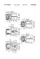
- FIG. 1is a schematic vertical sectional view of the vertical heat treatment apparatus according to one embodiment of the present invention.
- FIG. 2is a vertical sectional view of the rotary holder provided on the upper end of the loading mechanism of the vertical heat treatment apparatus of FIG. 1 and the liner plate provided on the loading mechanism.
- FIG. 3is a perspective view of the liner plate and the rotary holder of FIG. 2, and a lid.
- FIGS. 4A to 4Eare explanatory views of a sequence of the operation of the vertical heat treatment apparatus of FIG. 1.
- FIG. 1is a substantially general vertical sectional view of the vertical heat treatment apparatus according to this embodiment.
- This vertical heat treatment apparatusis used as an oxidation apparatus or a CVD apparatus for forming insulating films on an object to be treated, e.g., semiconductor wafers (hereinafter called wafers).
- waferssemiconductor wafers
- reference numeral 1represents a body of the apparatus of a closed box structure which ensures airtightness.
- An upper half of the interior of the body 1is a heat treatment chamber 2, and a lower half thereof is a loading chamber 4 where semiconductor wafers W as objects to be treated are loaded into and unloaded from the heat treatment chamber.
- the heat treatment chamber 2 and the loading chamber 4 of the body 1have their peripheral walls formed of a double wall structure of, e.g., stainless steel. Water can be passed between the inner and the outer walls, and a water jacket 5 is provided. Accordingly the interior of the body 1 is thermally isolated from the outside while high-temperature heat treatment can be conducted inside the heat treatment chamber without giving thermal influence to the outside. In addition, the efficiency of cooling the heat treated wafers W in the loading chamber 4 can be increased.
- the processing vessel 11is one kind of heating furnace and is formed of, e.g., quartz, which has good heat resistance and is less contaminative.
- the processing vessel 11is in the shape of a hat, i.e., a vertical substantial cylinder having a furnace port opened in the lower end with the upper end closed.
- a manifold 13 of substantially the same water cooling structure as described aboveis secured to a lower part of the outer periphery of the processing vessel 11 in the heat treatment chamber 2.
- the manifold 13partitions the heat treatment chamber 2 from the loading chamber 4.
- a discharge pipe 14 for evacuating to the outside (reducing a pressure) gases in the processing vessel 11and a gas feed pipe 15 for supplying required treatment gases from an outside gas supply source and an inert gas, such as N 2 gas or others, from above into the processing vessel 11.
- a first heater unit 21, a second heater unit 22, and a third heater units 23 as heat sourcesare provided around the processing vessel 11 in the heat treatment chamber 2.
- the first heater unit 21is arranged in plane above the processing vessel 11, and comprises a heater element 25 of lines of molybdenum dicilicide, KANTHAL (tradename) line of an iron, chrome and aluminum alloy or others arranged in plane as a plate heater on the underside of a substantially flat heat insulating plate 24 of, e.g. alumina ceramics or others, and a flat liner plate 26 provided inside the heater element 25.
- a heater element 25 of lines of molybdenum dicilicide, KANTHAL (tradename) line of an iron, chrome and aluminum alloy or othersarranged in plane as a plate heater on the underside of a substantially flat heat insulating plate 24 of, e.g. alumina ceramics or others, and a flat liner plate 26 provided inside the heater element 25.
- the liner plate 26functions to remove disuniform heating of the plate heater, i.e., disuniform distributions of radiation heat which has entered the processing vessel 11 from the heater element 25, and is formed of a material which is highly heat resistant to high temperature radiation heat and is less contaminative, e.g., silicon carbide, or quartz or graphite having the surface coated with silicon carbide.
- the second and the third heater units 22, 23are annular auxiliary heaters arranged respectively around an upper part and a middle part of the outside periphery of the processing vessel 11. Almost similarly with the first heater unit 21, the second and the third heater unit 22, 23 each comprise a heat insulating plate, a U-shaped heater element 28 arranged inside of the heat insulating plate 27 as a heater, and a heat liner plate 29 arranged on the inside of the heater element 28.
- the heat insulating plate 27 and the liner plate 29are cylindrical and the heater element 28 between the heat insulating plate and the heat liner plate 29 is provided by circumferentially arranged resistant heaters.
- the processing vessel 11can have inside, as shown in FIG. 4A, a first zone A which is uppermost for receiving incident heat energy mainly of the plate heater of the first heater unit 21, a second zone B which is the second zone for receiving incident heat energy mainly of the second heater unit 22, and a third zone C which is a middle zone of the processing vessel 11 for receiving incident heat energy mainly of the third heater unit 23.
- Heating temperatures of the first to the third zones A, B, Ccan be optionally set by power control of the first to the third heater units 21, 22, 23.
- a space between the outside circumferential surfaces of the first to the third heater units 21, 22, 23 and the inside surface of the body 1 of the apparatusis filled with a heat insulating material 29A, such as quartz wool or others for enhancing heat insulation from the outside.
- a heat insulating material 29Asuch as quartz wool or others for enhancing heat insulation from the outside.
- a loading mechanism 31which holds objects to be treated, wafers W, and loads/unloads the same one by one into/from the processing vessel] 1 through the bottom thereof.
- the loading mechanism 31comprises a lift drive unit 32, an outer cylindrical shaft 33 as a lift member which is driven by the lift drive unit 32 to be inserted into and out of the processing vessel 11 through the bottom thereof, a liner plate 34 provided on the upper end of the cylinder shaft 33, and a rotary holder 35 provided above the liner plate 34 for holding a wafer W.
- the outer cylindrical shaft 33is relatively thick and long, and hollow.
- the shaft 33is disposed upright along the central axial line of the furnace port in the bottom of the processing vessel 11 and is vertically movable through a bearing 37 inserted in the bottom of the loading chamber 4.
- the outer cylindrical shaft 33is driven up and down by the lift drive unit 32.
- the lift drive unit 32comprises a screw shaft 38 which is rotated clockwise and counter-clockwise by a motor 32A disposed below the loading chamber 4, and a lift support arm 39 which is in screw-engagement with the screw shaft 38 and is vertically moved by the screw.
- the outer cylindrical shaft 33is supported by the lift support arm 39 to be moved up and down.
- a stretchable bellows 40is provided between the bearing 37 and the lift support arm 39 for retaining air-tightness of the interior of the loading chamber 4 with respect to an outside atmosphere when the outer cylindrical shaft 37 is moved Up and down.
- the liner plate 34is also formed of a material, e.g., high purity silicon carbide (SiC) or quartz, which is highly heat resistant to high temperature radiation heat and is less contaminative. As shown in FIGS. 2 and 3, the liner plate is in the shape of a circular shallow dish having a raised peripheral edge 34a, is disposed horizontally on the upper end of the outer cylindrical shaft 33, and has an opening 34b in the center thereof, which is in communication with the interior of the outer cylindrical shaft 33.
- the liner plate 34has a diameter larger than an outside dimension of the wafer W by ⁇ (about 30 mm) for the prevention of cooling of a wafer W when the wafer W is lifted up and down.
- the rotary holder 35has a central rotary shaft 42. As shown in FIGS. 2 and 3, a plurality (e.g., 4) of slender support rods 43 which are projected radially from the upper end of the rotary central shaft 42 and disposed circumferentially at a certain interval. A small length of the forward end of each support rod 43 is bent upward in an L shape, and the forward end is cut off, declined inward in a slant surface 43a.
- the respective slant surfaces 43areceive the lower outer peripheral portion (edge) of the wafer W at four positions to hold the wafer W horizontal above the liner plate 34.
- the rotary holder 35is also formed of a material which is highly heat resistant to high temperature radiation heat and is less contaminative, e.g., high purity silicon carbide (SiC) or quartz.
- the rotary central shaft 42 of the rotary holder 35has a small diameter and is long, and is put rotatably and vertically movably through a central opening of the liner plate 34 and the outer cylindrical shaft 33.
- the rotary central shaft 42is jutted more downward beyond the outer cylindrical shaft 33 and is supported by a lift support arm 46 of a sub-lift drive unit 45 mounted on the lift support arm of the lift drive unit 32.
- the rotary holder 35is moved up and down together with the outer cylindrical shaft 33 through the rotary central shaft 42, and is moved up and down alone quickly by screwing of the screw shaft 48 rotated clockwise and counter-clockwise by the motor 47 of the sub-lift drive unit 45.
- a stretchable bellows 49is provided between the lower end of the outer cylindrical shaft 33 and the lift support arm 46 for retaining air-tightness of the interior of the lower end portion of the outer cylindrical shaft 33 with respect to an outside atmosphere when the rotary central haft 42 is moved up and down.
- the rotary central shaft 42 of the rotary holder 35is rotated by gears 53, 54 by the drive of the motor 52 of a rotation drive motor 51 mounted on the lift support arm 46 of the sub-lift drive unit.
- the loading mechanism 31 with a wafer W held in a horizontal orientation on the rotary holder 35 above the liner plate 34is lifted together with the outer cylindrical shaft 33 to be loaded into the processing vessel 11. Further the rotary holder 35 independently moves up and down in the processing vessel 11 so as to quickly displace the wafer W from a high-temperature heating position (e.g., the A zone) to a suitable temperature treating position (e.g., the B zone) as shown in FIG. 4.
- a high-temperature heating positione.g., the A zone
- a suitable temperature treating positione.g., the B zone
- the loading mechanism 31has a lid 55 provided on the outer cylindrical shaft 33 at a position nearer to the upper end thereof for gas sealing and heat shielding for the interior of the processing vessel 11 during a heat treatment of a wafer W.
- the lid 55is brought into contact with the furnace port in the bottom of the processing vessel 11 through a seal member 55A to place the interior of the processing vessel 11 in a completely sealed condition with respect to the loading chamber 4.
- On the upper surface of the lid 55there is provided a hollow annular water cooling disk 56. Water can be circulated through the water cooling disk 56 through the outer cylindrical shaft 33 by water feed hoses 57, 58 provided in the lower end portion of the outer cylindrical portion.
- a plurality of thin reflectors 59 of quartz in the form of heat radiation finsare secured to an upper part of the water cooling disk 56 in multi-steps by soldering or others.
- the loading mechanism 31has gas injection means for injecting a trace of a film formation preventive gas for the prevention of formation of a film on the underside of a wafer W when the wafer W is heat treated in the processing vessel 11.
- the gas injection meansis a gas conduit 61 between the outer cylindrical shaft 33 and the rotary central shaft 42 over a length thereof, whose upper end is in communication with the central opening 34b of the liner plate 34 and whose lower end is in communication with the interior of the bellows 49 shown in FIG. 1.
- a gas hose 62is connected to the bellows 49 for introducing the film formation preventing gas into the bellows 49 from the outside.
- the rotary central shaft 42is also hollow, and a temperature sensor 63 is inserted in the rotary central shaft 42 from below so that temperatures of a wafer W mounted on the rotary holder 35 are detected for various controls.
- the interior of the loading chamber 4has a closed structure (isolated from the atmospheric air) under an atmosphere of an inert gas (nonoxygen atmosphere), such as N 2 gas or others.
- gas feed nozzles 65, 66 for feeding N 2 gasare provided as the gas feed means, and gas exhaust pipes 67, 68 are provided on the opposite inside.
- a load lock chamber 70is provided for continuously conveying wafers W as objects to be processed into the loading chamber 4, isolated from the atmospheric air.
- the load lock chamber 70has a relatively small box shape so as to facilitate displacement of atmospheric air with an inert gas, and is connected at the top to a gas feed pipe 71 for N 2 gas or others and at the bottom to an exhaust pipe 72.
- Gate valves 73, 74are provided on the left and the right sides of the load lock chamber 70.
- a buffer 75for temporarily mounting wafers W and a transfer mechanism (a handling robot) 76.
- the gate valve 73is opened and wafers W are put onto the buffer 75 in the load lock chamber 70 from the outside by a conveying robot or others. With the gate valve 73 closed, the interior of the load lock chamber 70 is placed under an atmosphere of an inert gas. Then the other gate valve 74 is opened to transfer the wafers W one by one by the transfer mechanism 76 onto the rotary holder 35 of the loading mechanism 31 in the loading chamber 4. The treated wafers W are taken outside by the reverse procedure. Accordingly the loading operation of wafers W from the loading chamber 4 into the processing vessel 11, and the unloading operation reverse to the load operation can be conducted throughout in an atmosphere of an inert gas, such as N 2 gas isolated from the outside atmospheric air.
- an inert gassuch as N 2 gas isolated from the outside atmospheric air.
- a total of two load lock chambers 70are preferably provided on the loading chamber 4 at opposing front and back positions (only one shown in FIG. 1), so that wafers W can be conveyed in a one-way manner.
- An inverted E-shaped box 80 covered with a water jacketis provided on a side of the loading chamber 4, continuously opened in the loading chamber 4.
- the box 80accommodates a furnace port shutter 81 of a sectional shape which is made of a material of high heat resistance and heat insulation and can close the furnace port, and a partition shutter 82 which can partition the interior of the loading chamber 4 vertically in an upper part and a lower part.
- the furnace port shutter 81 and the partition shutter 82are disposed parallel with each other at a vertical interval from each other and each have one end thereof supportably connected to a rod 85 of an air cylinder 84 of a swing/lift drive mechanism 83.
- the swing/lift mechanism 83has an air cylinder 84 for lift, and a motor 86 and spline gears 87, 88 for the swing which rotate the rod 85.
- the partition shutter 82has an arcuate groove 82a formed in the middle thereof.
- the arcuate groove 82areceives the rotary central shaft 42 of the loading mechanism 31 which has been lowered and partitions the interior of the loading chamber 4 up and down between the liner plate 34 and the rotary holder 35.
- the furnace port shutter 81 and the partition shutter 82are formed in hollow discs. Water is circulated through the hollow discs through the rod 85 from water hoses 89, 90 provided in the lower part of the rod 85, and a water cooling structure is provided.
- the motors 47, 52, 86, and the motor 32A of the lift drive unit 32are controlled by control means 100, based on data stored in a memory unit 101.
- furnace port shutter 81 and the partition shutter 82are retreated in the box 80 as in FIG. 4A, and loading mechanism 31 is lifted as in FIG. 4C and loads the wafers into processing chamber 11 while the furnace port in the bottom of the processing vessel 11 is closed by the lid 55.
- the first heater 21 on the top of the processing tube 11is controlled to retain a constant high heating temperature of about 1200° C. and sets the first zone A, which is the uppermost, at a highest-temperature heating position.
- the second heater unit 22, which is around an upper outside periphery of the processing vessel 11,is controlled to at first have a high temperature and then to lower the temperature to about 800° C. when a wafer comes up, so that the second zone B, which is next uppermost, has a suitable treating temperature.
- the third heater unit 23, which is around the middle outside periphery of the processing vessel 11,is controlled to at first have a high temperature and lower the temperature to about 800° C. when a wafer comes up, so that the third middle zone C is set at a suitable heat retaining temperature.
- the rotary holder 35 on the upper end of the outer cylindrical shaft 33 and above the liner plate 34 with a wafer W mounted on horizontalis lifted to the second zone B in the thus heated processing vessel 11. Even when the wafer has a large diameter, owing to the liner effect of the liner plate 34 and the rotation of the rotary holder 35, the wafer W can be efficiently heated with a substantially uniform temperature distribution in plane substantially without circumferentially local disuniform temperatures, and temperature differences between the central part and the peripheral part.
- the rotary holder 35is lifted independently from the liner plate 34, turning the wafer W, to the first uppermost zone for the above-described high-temperature heating.
- the wafer Wis rapidly heated and is lowered to the zone B set as a suitable temperature treatment position when the wafer W reaches a set treating temperature.
- the wafer which has been thus heated to a set treating temperatureis stopped in the second zone set as a suitable treating temperature zone, and as shown in FIG. 4E, N 2 gas in the processing vessel 11 is exhausted while required treating gases are fed from above, and the surface of the wafer W is subjected to a required heat treatment (film formation).
- a film formation preventive gasis fed into the gas passage 61 from the gas hose 62 in the lower part of the loading mechanism 31.
- the gasis injected bit by bit from the central opening 34b in the liner plate 34 as shown in FIG. 2 onto the underside of the wafer W.
- the film formation preventive gasflows through a gap between the liner plate 34 and the wafer W to thereby prohibit the treatment gases from flowing into the underside of the wafer W, whereby the formation of films on the underside of the wafer W is prevented, i.e., films can be formed only on the surface of the wafer W without forming films on the unnecessary surface.
- the treatment gases in the processing vessel 11are evacuated, and an inert gas, such as N 2 gas is fed into the interior of the processing vessel 11 to purge the same.
- an inert gassuch as N 2 gas is fed into the interior of the processing vessel 11 to purge the same.
- the treated wafer Wis conveyed out in the procedure substantially reverse to that for conveying in the wafer W.
- the loading mechanism 31When the wafer W is conveyed out, the loading mechanism 31 is lowered to draw the wafer W out of the processing vessel 11 into the loading chamber 4. At this time, with the rotary holder 35 holding the wafer W retained at substantially the same height as the load lock chamber 70, the outer rotary shaft 33 is further lowered to the state as shown in FIG. 4A. In this state, the furnace port shutter 81 and the partition shutter 82 are advanced into the loading lock chamber 4, and swung and raised. And the upper furnace port shutter 81 closes the furnace port in the bottom of the processing vessel 11, so that little heat escapes from the interior of the processing vessel 11 into the loading chamber 4.
- the lower partition shutter 82partitions the interior of the loading chamber up and down between the liner plate 34 and the rotary holder 35, so that the treated wafer W at the high temperature, and the liner plate 34 and the reflectors 59 of the loading mechanism 31 at the same high temperature are separated from each other to be separately cooled efficiently by introduction of an inert gas from the upper and lower gas feed pipes 65, 66 and suction exhaust thereof through the gas exhaust pipes 67, 68.
- the thus-treated wafer Wis conveyed outside through the load lock chamber 70.
- the vertical heat treatment apparatusis used as an oxidation apparatus or CVD apparatus for forming insulating films on semiconductor wafers W as objects to be treated.
- kinds of objects to be treated and kinds of treatmentsare not especially limited and may be treatment apparatuses for conducting treatments on other kinds, such as LCD substrates, etc.
- inert gasesmay be fed in accordance with the kind of treatment.
- the treatment gaswhen the apparatus is used as a CVD apparatus to form polysilicon films, may be SiH 4 , and when silicon nitride films are formed, NH 4 , and SiH 2 Cl 2 gas are used.
- the heating capacities of the respective heater unit 21-32may be decided in accordance with treatments. For example, for the case of an oxidation apparatus, a treating temperature is set at 800°-1200° C., and for the case of a CVD apparatus, a treating temperature is set at 500°-1200° C.
- large objects to be treatedsuch as large-diameter semiconductor wafers, LCD substrates, etc. can be rapidly heated up to a set treating temperature while achieving uniform temperature distributions in plane and heat treatments of high precision can be conducted.
Landscapes
- Chemical & Material Sciences (AREA)
- Engineering & Computer Science (AREA)
- Materials Engineering (AREA)
- Metallurgy (AREA)
- Organic Chemistry (AREA)
- Chemical Kinetics & Catalysis (AREA)
- General Chemical & Material Sciences (AREA)
- Crystallography & Structural Chemistry (AREA)
- Health & Medical Sciences (AREA)
- Toxicology (AREA)
- Physics & Mathematics (AREA)
- Condensed Matter Physics & Semiconductors (AREA)
- General Physics & Mathematics (AREA)
- Manufacturing & Machinery (AREA)
- Computer Hardware Design (AREA)
- Microelectronics & Electronic Packaging (AREA)
- Power Engineering (AREA)
- Mechanical Engineering (AREA)
Abstract
Description
Claims (8)
Applications Claiming Priority (2)
| Application Number | Priority Date | Filing Date | Title |
|---|---|---|---|
| JP08634093AJP3190165B2 (en) | 1993-04-13 | 1993-04-13 | Vertical heat treatment apparatus and heat treatment method |
| JP5-086340 | 1993-04-13 |
Publications (1)
| Publication Number | Publication Date |
|---|---|
| US5443648Atrue US5443648A (en) | 1995-08-22 |
Family
ID=13884129
Family Applications (1)
| Application Number | Title | Priority Date | Filing Date |
|---|---|---|---|
| US08/225,618Expired - Fee RelatedUS5443648A (en) | 1993-04-13 | 1994-04-11 | Vertical heat treatment apparatus with a rotary holder turning independently of a liner plate |
Country Status (3)
| Country | Link |
|---|---|
| US (1) | US5443648A (en) |
| JP (1) | JP3190165B2 (en) |
| KR (1) | KR100359351B1 (en) |
Cited By (318)
| Publication number | Priority date | Publication date | Assignee | Title |
|---|---|---|---|---|
| EP0735575A1 (en)* | 1995-03-31 | 1996-10-02 | Asm International N.V. | Vertical furnace |
| US5632820A (en)* | 1995-01-12 | 1997-05-27 | Kokusai Electric Co., Ltd. | Thermal treatment furnace in a system for manufacturing semiconductors |
| US5695568A (en)* | 1993-04-05 | 1997-12-09 | Applied Materials, Inc. | Chemical vapor deposition chamber |
| NL1005410C2 (en)* | 1997-02-28 | 1998-08-31 | Advanced Semiconductor Mat | System for loading, handling and unloading substrates mounted on a support. |
| US5899653A (en)* | 1997-06-23 | 1999-05-04 | Applied Materials, Inc. | Two-stage vacuum bellows |
| US5938852A (en)* | 1996-05-17 | 1999-08-17 | Samsung Electronics Co., Ltd. | Cap for vertical furnace |
| US5948300A (en)* | 1997-09-12 | 1999-09-07 | Kokusai Bti Corporation | Process tube with in-situ gas preheating |
| US6036482A (en)* | 1995-02-10 | 2000-03-14 | Tokyo Electron Limited | Heat treatment method |
| US6074486A (en)* | 1997-04-22 | 2000-06-13 | Samsung Electronics Co., Ltd. | Apparatus and method for manufacturing a semiconductor device having hemispherical grains |
| US6210483B1 (en) | 1997-12-02 | 2001-04-03 | Applied Materials, Inc. | Anti-notch thinning heater |
| US6322631B1 (en) | 1995-02-10 | 2001-11-27 | Tokyo Electron Limited | Heat treatment method and its apparatus |
| US20020034595A1 (en)* | 2000-09-19 | 2002-03-21 | Kouji Tometsuka | Substrate processing equipment and method and covering member for use therein |
| US6369361B2 (en)* | 2000-01-28 | 2002-04-09 | Tokyo Electron Limited | Thermal processing apparatus |
| WO2002076640A1 (en)* | 2001-03-27 | 2002-10-03 | Semitool, Inc. | Vertical process reactor |
| US6483081B1 (en)* | 2000-11-27 | 2002-11-19 | Novellus Systems, Inc. | In-line cure furnace and method for using the same |
| US6506252B2 (en) | 2001-02-07 | 2003-01-14 | Emcore Corporation | Susceptorless reactor for growing epitaxial layers on wafers by chemical vapor deposition |
| US20030031974A1 (en)* | 2001-07-26 | 2003-02-13 | Mikio Takagi | Heating furnace and semiconductor wafer-holding jig assembly and process of manufacturing semiconductor devices |
| US6582780B1 (en)* | 1999-08-30 | 2003-06-24 | Si Diamond Technology, Inc. | Substrate support for use in a hot filament chemical vapor deposition chamber |
| US20030140853A1 (en)* | 2002-01-21 | 2003-07-31 | Hitachi Kokusai Electric Inc. | Substrate processing apparatus |
| US6673673B1 (en) | 1997-04-22 | 2004-01-06 | Samsung Electronics Co., Ltd. | Method for manufacturing a semiconductor device having hemispherical grains |
| EP0840358A3 (en)* | 1996-11-05 | 2004-01-14 | Applied Materials, Inc. | Sloped substrate support |
| US6692209B1 (en)* | 1999-11-19 | 2004-02-17 | Litton Systems, Inc. | Method and system for manufacturing a photocathode |
| US6709520B1 (en)* | 1998-11-25 | 2004-03-23 | Centre National De La Recherche Scientifique (Cnrs) | Reactor and method for chemical vapor deposition |
| US6752874B2 (en)* | 2000-10-12 | 2004-06-22 | Electronics And Telecommunications Research Institute | Apparatus for perpendicular-type ultra vacuum chemical vapor deposition |
| US20040164504A1 (en)* | 2003-02-21 | 2004-08-26 | Igor Ivanov | Universal substrate holder for treating objects in fluids |
| US20050042807A1 (en)* | 2003-08-22 | 2005-02-24 | Axcelis Technologies, Inc. | Method of positioning an elevator tube |
| US20050051196A1 (en)* | 2003-09-08 | 2005-03-10 | Taiwan Semiconductor Manufacturing Co., Ltd., | Developer dispensing apparatus with adjustable knife ring |
| CN100356505C (en)* | 2003-12-26 | 2007-12-19 | 清华大学 | Fast semiconductor heat-treating facility with vertical heat treating chamber |
| US20090064934A1 (en)* | 2007-09-07 | 2009-03-12 | Beom Soo Park | Source gas flow path control in pecvd system to control a by-product film deposition on inside chamber |
| US20090078694A1 (en)* | 2007-09-20 | 2009-03-26 | Tokyo Electron Limited | Substrate processing apparatus and substrate stage used therein |
| US20090178620A1 (en)* | 2002-04-22 | 2009-07-16 | Holger Juergensen | Process for Depositing Thin Layers on a Substrate in a Process Chamber of Adjustable Height |
| US20090178614A1 (en)* | 2001-02-09 | 2009-07-16 | Tokyo Electron Limited | Film-forming apparatus |
| US20100012035A1 (en)* | 2006-09-11 | 2010-01-21 | Hiroshi Nagata | Vacuum vapor processing apparatus |
| US20100186667A1 (en)* | 2009-01-26 | 2010-07-29 | Tokyo Electron Limited | Vertical heat processing apparatus and component for same, for forming high dielectric constant film |
| US20120070577A1 (en)* | 2010-09-22 | 2012-03-22 | Deura Kaori | Film-forming apparatus and film-forming method |
| US20120220108A1 (en)* | 2011-02-28 | 2012-08-30 | Hitachi Kokusai Electric Inc. | Substrate processing apparatus, and method of manufacturing substrate |
| US20130092086A1 (en)* | 2011-10-17 | 2013-04-18 | Novellus Systems, Inc. | Mechanical suppression of parasitic plasma in substrate processing chamber |
| US20130298830A1 (en)* | 2008-01-30 | 2013-11-14 | Palo Alto Research Center, Incorporated | Growth reactor systems and methods for low-temperature synthesis of nanowires |
| US20140051258A1 (en)* | 2012-08-17 | 2014-02-20 | Dainippon Screen Mfg. Co., Ltd. | Substrate processing device and substrate processing method for carrying out chemical treatment for substrate |
| US20140051259A1 (en)* | 2012-08-20 | 2014-02-20 | Dainippon Screen Mfg. Co., Ltd. | Substrate processing device and substrate processing method for carrying out chemical treatment for substrate |
| US20140345525A1 (en)* | 2013-05-23 | 2014-11-27 | Applied Materials, Inc. | Coated liner assembly for a semiconductor processing chamber |
| US20150329967A1 (en)* | 2010-08-27 | 2015-11-19 | Nuflare Technology, Inc. | Film-forming manufacturing apparatus and method |
| US11004977B2 (en) | 2017-07-19 | 2021-05-11 | Asm Ip Holding B.V. | Method for depositing a group IV semiconductor and related semiconductor device structures |
| US11001925B2 (en) | 2016-12-19 | 2021-05-11 | Asm Ip Holding B.V. | Substrate processing apparatus |
| US11018002B2 (en) | 2017-07-19 | 2021-05-25 | Asm Ip Holding B.V. | Method for selectively depositing a Group IV semiconductor and related semiconductor device structures |
| US11015245B2 (en) | 2014-03-19 | 2021-05-25 | Asm Ip Holding B.V. | Gas-phase reactor and system having exhaust plenum and components thereof |
| US11022879B2 (en) | 2017-11-24 | 2021-06-01 | Asm Ip Holding B.V. | Method of forming an enhanced unexposed photoresist layer |
| US11031242B2 (en) | 2018-11-07 | 2021-06-08 | Asm Ip Holding B.V. | Methods for depositing a boron doped silicon germanium film |
| USD922229S1 (en) | 2019-06-05 | 2021-06-15 | Asm Ip Holding B.V. | Device for controlling a temperature of a gas supply unit |
| US11049751B2 (en) | 2018-09-14 | 2021-06-29 | Asm Ip Holding B.V. | Cassette supply system to store and handle cassettes and processing apparatus equipped therewith |
| US11053591B2 (en) | 2018-08-06 | 2021-07-06 | Asm Ip Holding B.V. | Multi-port gas injection system and reactor system including same |
| US11056344B2 (en) | 2017-08-30 | 2021-07-06 | Asm Ip Holding B.V. | Layer forming method |
| US11069510B2 (en) | 2017-08-30 | 2021-07-20 | Asm Ip Holding B.V. | Substrate processing apparatus |
| US11081345B2 (en) | 2018-02-06 | 2021-08-03 | Asm Ip Holding B.V. | Method of post-deposition treatment for silicon oxide film |
| US11087997B2 (en) | 2018-10-31 | 2021-08-10 | Asm Ip Holding B.V. | Substrate processing apparatus for processing substrates |
| US11088002B2 (en) | 2018-03-29 | 2021-08-10 | Asm Ip Holding B.V. | Substrate rack and a substrate processing system and method |
| US11094582B2 (en) | 2016-07-08 | 2021-08-17 | Asm Ip Holding B.V. | Selective deposition method to form air gaps |
| US11094546B2 (en) | 2017-10-05 | 2021-08-17 | Asm Ip Holding B.V. | Method for selectively depositing a metallic film on a substrate |
| US11101370B2 (en) | 2016-05-02 | 2021-08-24 | Asm Ip Holding B.V. | Method of forming a germanium oxynitride film |
| US11107676B2 (en) | 2016-07-28 | 2021-08-31 | Asm Ip Holding B.V. | Method and apparatus for filling a gap |
| US11114294B2 (en) | 2019-03-08 | 2021-09-07 | Asm Ip Holding B.V. | Structure including SiOC layer and method of forming same |
| US11114283B2 (en) | 2018-03-16 | 2021-09-07 | Asm Ip Holding B.V. | Reactor, system including the reactor, and methods of manufacturing and using same |
| USD930782S1 (en) | 2019-08-22 | 2021-09-14 | Asm Ip Holding B.V. | Gas distributor |
| US11127589B2 (en) | 2019-02-01 | 2021-09-21 | Asm Ip Holding B.V. | Method of topology-selective film formation of silicon oxide |
| US11127617B2 (en) | 2017-11-27 | 2021-09-21 | Asm Ip Holding B.V. | Storage device for storing wafer cassettes for use with a batch furnace |
| USD931978S1 (en) | 2019-06-27 | 2021-09-28 | Asm Ip Holding B.V. | Showerhead vacuum transport |
| US11139191B2 (en) | 2017-08-09 | 2021-10-05 | Asm Ip Holding B.V. | Storage apparatus for storing cassettes for substrates and processing apparatus equipped therewith |
| US11139308B2 (en) | 2015-12-29 | 2021-10-05 | Asm Ip Holding B.V. | Atomic layer deposition of III-V compounds to form V-NAND devices |
| US11158513B2 (en) | 2018-12-13 | 2021-10-26 | Asm Ip Holding B.V. | Methods for forming a rhenium-containing film on a substrate by a cyclical deposition process and related semiconductor device structures |
| US11164955B2 (en) | 2017-07-18 | 2021-11-02 | Asm Ip Holding B.V. | Methods for forming a semiconductor device structure and related semiconductor device structures |
| US11168395B2 (en) | 2018-06-29 | 2021-11-09 | Asm Ip Holding B.V. | Temperature-controlled flange and reactor system including same |
| USD935572S1 (en) | 2019-05-24 | 2021-11-09 | Asm Ip Holding B.V. | Gas channel plate |
| US11171025B2 (en) | 2019-01-22 | 2021-11-09 | Asm Ip Holding B.V. | Substrate processing device |
| US11205585B2 (en) | 2016-07-28 | 2021-12-21 | Asm Ip Holding B.V. | Substrate processing apparatus and method of operating the same |
| US11217444B2 (en) | 2018-11-30 | 2022-01-04 | Asm Ip Holding B.V. | Method for forming an ultraviolet radiation responsive metal oxide-containing film |
| USD940837S1 (en) | 2019-08-22 | 2022-01-11 | Asm Ip Holding B.V. | Electrode |
| US11222772B2 (en) | 2016-12-14 | 2022-01-11 | Asm Ip Holding B.V. | Substrate processing apparatus |
| US11227789B2 (en) | 2019-02-20 | 2022-01-18 | Asm Ip Holding B.V. | Method and apparatus for filling a recess formed within a substrate surface |
| US11227782B2 (en) | 2019-07-31 | 2022-01-18 | Asm Ip Holding B.V. | Vertical batch furnace assembly |
| US11230766B2 (en) | 2018-03-29 | 2022-01-25 | Asm Ip Holding B.V. | Substrate processing apparatus and method |
| US11232963B2 (en) | 2018-10-03 | 2022-01-25 | Asm Ip Holding B.V. | Substrate processing apparatus and method |
| US11233133B2 (en) | 2015-10-21 | 2022-01-25 | Asm Ip Holding B.V. | NbMC layers |
| US11242598B2 (en) | 2015-06-26 | 2022-02-08 | Asm Ip Holding B.V. | Structures including metal carbide material, devices including the structures, and methods of forming same |
| US11244825B2 (en) | 2018-11-16 | 2022-02-08 | Asm Ip Holding B.V. | Methods for depositing a transition metal chalcogenide film on a substrate by a cyclical deposition process |
| US11251035B2 (en) | 2016-12-22 | 2022-02-15 | Asm Ip Holding B.V. | Method of forming a structure on a substrate |
| US11251040B2 (en) | 2019-02-20 | 2022-02-15 | Asm Ip Holding B.V. | Cyclical deposition method including treatment step and apparatus for same |
| US11248295B2 (en) | 2014-01-27 | 2022-02-15 | Veeco Instruments Inc. | Wafer carrier having retention pockets with compound radii for chemical vapor deposition systems |
| US11251068B2 (en) | 2018-10-19 | 2022-02-15 | Asm Ip Holding B.V. | Substrate processing apparatus and substrate processing method |
| USD944946S1 (en) | 2019-06-14 | 2022-03-01 | Asm Ip Holding B.V. | Shower plate |
| US11270899B2 (en) | 2018-06-04 | 2022-03-08 | Asm Ip Holding B.V. | Wafer handling chamber with moisture reduction |
| US11274369B2 (en) | 2018-09-11 | 2022-03-15 | Asm Ip Holding B.V. | Thin film deposition method |
| US11282698B2 (en) | 2019-07-19 | 2022-03-22 | Asm Ip Holding B.V. | Method of forming topology-controlled amorphous carbon polymer film |
| US11286558B2 (en) | 2019-08-23 | 2022-03-29 | Asm Ip Holding B.V. | Methods for depositing a molybdenum nitride film on a surface of a substrate by a cyclical deposition process and related semiconductor device structures including a molybdenum nitride film |
| US11289326B2 (en) | 2019-05-07 | 2022-03-29 | Asm Ip Holding B.V. | Method for reforming amorphous carbon polymer film |
| US11286562B2 (en) | 2018-06-08 | 2022-03-29 | Asm Ip Holding B.V. | Gas-phase chemical reactor and method of using same |
| US11296189B2 (en) | 2018-06-21 | 2022-04-05 | Asm Ip Holding B.V. | Method for depositing a phosphorus doped silicon arsenide film and related semiconductor device structures |
| USD947913S1 (en) | 2019-05-17 | 2022-04-05 | Asm Ip Holding B.V. | Susceptor shaft |
| US11295980B2 (en) | 2017-08-30 | 2022-04-05 | Asm Ip Holding B.V. | Methods for depositing a molybdenum metal film over a dielectric surface of a substrate by a cyclical deposition process and related semiconductor device structures |
| USD948463S1 (en) | 2018-10-24 | 2022-04-12 | Asm Ip Holding B.V. | Susceptor for semiconductor substrate supporting apparatus |
| USD949319S1 (en) | 2019-08-22 | 2022-04-19 | Asm Ip Holding B.V. | Exhaust duct |
| US11306395B2 (en) | 2017-06-28 | 2022-04-19 | Asm Ip Holding B.V. | Methods for depositing a transition metal nitride film on a substrate by atomic layer deposition and related deposition apparatus |
| US11315794B2 (en) | 2019-10-21 | 2022-04-26 | Asm Ip Holding B.V. | Apparatus and methods for selectively etching films |
| US11342216B2 (en) | 2019-02-20 | 2022-05-24 | Asm Ip Holding B.V. | Cyclical deposition method and apparatus for filling a recess formed within a substrate surface |
| US11339476B2 (en) | 2019-10-08 | 2022-05-24 | Asm Ip Holding B.V. | Substrate processing device having connection plates, substrate processing method |
| US11345999B2 (en) | 2019-06-06 | 2022-05-31 | Asm Ip Holding B.V. | Method of using a gas-phase reactor system including analyzing exhausted gas |
| US11355338B2 (en) | 2019-05-10 | 2022-06-07 | Asm Ip Holding B.V. | Method of depositing material onto a surface and structure formed according to the method |
| US11361990B2 (en) | 2018-05-28 | 2022-06-14 | Asm Ip Holding B.V. | Substrate processing method and device manufactured by using the same |
| US11374112B2 (en) | 2017-07-19 | 2022-06-28 | Asm Ip Holding B.V. | Method for depositing a group IV semiconductor and related semiconductor device structures |
| US11378337B2 (en) | 2019-03-28 | 2022-07-05 | Asm Ip Holding B.V. | Door opener and substrate processing apparatus provided therewith |
| US11387120B2 (en) | 2017-09-28 | 2022-07-12 | Asm Ip Holding B.V. | Chemical dispensing apparatus and methods for dispensing a chemical to a reaction chamber |
| US11387106B2 (en) | 2018-02-14 | 2022-07-12 | Asm Ip Holding B.V. | Method for depositing a ruthenium-containing film on a substrate by a cyclical deposition process |
| US11390945B2 (en) | 2019-07-03 | 2022-07-19 | Asm Ip Holding B.V. | Temperature control assembly for substrate processing apparatus and method of using same |
| US11393690B2 (en) | 2018-01-19 | 2022-07-19 | Asm Ip Holding B.V. | Deposition method |
| US11390946B2 (en) | 2019-01-17 | 2022-07-19 | Asm Ip Holding B.V. | Methods of forming a transition metal containing film on a substrate by a cyclical deposition process |
| US11393703B2 (en)* | 2018-06-18 | 2022-07-19 | Applied Materials, Inc. | Apparatus and method for controlling a flow process material to a deposition chamber |
| US11390950B2 (en) | 2017-01-10 | 2022-07-19 | Asm Ip Holding B.V. | Reactor system and method to reduce residue buildup during a film deposition process |
| US11396702B2 (en) | 2016-11-15 | 2022-07-26 | Asm Ip Holding B.V. | Gas supply unit and substrate processing apparatus including the gas supply unit |
| US11398382B2 (en) | 2018-03-27 | 2022-07-26 | Asm Ip Holding B.V. | Method of forming an electrode on a substrate and a semiconductor device structure including an electrode |
| US11401605B2 (en) | 2019-11-26 | 2022-08-02 | Asm Ip Holding B.V. | Substrate processing apparatus |
| US11410851B2 (en) | 2017-02-15 | 2022-08-09 | Asm Ip Holding B.V. | Methods for forming a metallic film on a substrate by cyclical deposition and related semiconductor device structures |
| US11411088B2 (en) | 2018-11-16 | 2022-08-09 | Asm Ip Holding B.V. | Methods for forming a metal silicate film on a substrate in a reaction chamber and related semiconductor device structures |
| US11417545B2 (en) | 2017-08-08 | 2022-08-16 | Asm Ip Holding B.V. | Radiation shield |
| US11414760B2 (en) | 2018-10-08 | 2022-08-16 | Asm Ip Holding B.V. | Substrate support unit, thin film deposition apparatus including the same, and substrate processing apparatus including the same |
| US11424119B2 (en) | 2019-03-08 | 2022-08-23 | Asm Ip Holding B.V. | Method for selective deposition of silicon nitride layer and structure including selectively-deposited silicon nitride layer |
| US11430674B2 (en) | 2018-08-22 | 2022-08-30 | Asm Ip Holding B.V. | Sensor array, apparatus for dispensing a vapor phase reactant to a reaction chamber and related methods |
| US11430640B2 (en) | 2019-07-30 | 2022-08-30 | Asm Ip Holding B.V. | Substrate processing apparatus |
| US11437241B2 (en) | 2020-04-08 | 2022-09-06 | Asm Ip Holding B.V. | Apparatus and methods for selectively etching silicon oxide films |
| US11443926B2 (en) | 2019-07-30 | 2022-09-13 | Asm Ip Holding B.V. | Substrate processing apparatus |
| US11447864B2 (en) | 2019-04-19 | 2022-09-20 | Asm Ip Holding B.V. | Layer forming method and apparatus |
| US11447861B2 (en) | 2016-12-15 | 2022-09-20 | Asm Ip Holding B.V. | Sequential infiltration synthesis apparatus and a method of forming a patterned structure |
| USD965044S1 (en) | 2019-08-19 | 2022-09-27 | Asm Ip Holding B.V. | Susceptor shaft |
| US11453943B2 (en) | 2016-05-25 | 2022-09-27 | Asm Ip Holding B.V. | Method for forming carbon-containing silicon/metal oxide or nitride film by ALD using silicon precursor and hydrocarbon precursor |
| USD965524S1 (en) | 2019-08-19 | 2022-10-04 | Asm Ip Holding B.V. | Susceptor support |
| US11469098B2 (en) | 2018-05-08 | 2022-10-11 | Asm Ip Holding B.V. | Methods for depositing an oxide film on a substrate by a cyclical deposition process and related device structures |
| US11473195B2 (en) | 2018-03-01 | 2022-10-18 | Asm Ip Holding B.V. | Semiconductor processing apparatus and a method for processing a substrate |
| US11476109B2 (en) | 2019-06-11 | 2022-10-18 | Asm Ip Holding B.V. | Method of forming an electronic structure using reforming gas, system for performing the method, and structure formed using the method |
| US11482418B2 (en) | 2018-02-20 | 2022-10-25 | Asm Ip Holding B.V. | Substrate processing method and apparatus |
| US11482412B2 (en) | 2018-01-19 | 2022-10-25 | Asm Ip Holding B.V. | Method for depositing a gap-fill layer by plasma-assisted deposition |
| US11482533B2 (en) | 2019-02-20 | 2022-10-25 | Asm Ip Holding B.V. | Apparatus and methods for plug fill deposition in 3-D NAND applications |
| US11488819B2 (en) | 2018-12-04 | 2022-11-01 | Asm Ip Holding B.V. | Method of cleaning substrate processing apparatus |
| US11488854B2 (en) | 2020-03-11 | 2022-11-01 | Asm Ip Holding B.V. | Substrate handling device with adjustable joints |
| US11495459B2 (en) | 2019-09-04 | 2022-11-08 | Asm Ip Holding B.V. | Methods for selective deposition using a sacrificial capping layer |
| US11492703B2 (en) | 2018-06-27 | 2022-11-08 | Asm Ip Holding B.V. | Cyclic deposition methods for forming metal-containing material and films and structures including the metal-containing material |
| US11499226B2 (en) | 2018-11-02 | 2022-11-15 | Asm Ip Holding B.V. | Substrate supporting unit and a substrate processing device including the same |
| US11501968B2 (en) | 2019-11-15 | 2022-11-15 | Asm Ip Holding B.V. | Method for providing a semiconductor device with silicon filled gaps |
| US11499222B2 (en) | 2018-06-27 | 2022-11-15 | Asm Ip Holding B.V. | Cyclic deposition methods for forming metal-containing material and films and structures including the metal-containing material |
| US11501973B2 (en) | 2018-01-16 | 2022-11-15 | Asm Ip Holding B.V. | Method for depositing a material film on a substrate within a reaction chamber by a cyclical deposition process and related device structures |
| US11501956B2 (en) | 2012-10-12 | 2022-11-15 | Asm Ip Holding B.V. | Semiconductor reaction chamber showerhead |
| US11515188B2 (en) | 2019-05-16 | 2022-11-29 | Asm Ip Holding B.V. | Wafer boat handling device, vertical batch furnace and method |
| US11515187B2 (en) | 2020-05-01 | 2022-11-29 | Asm Ip Holding B.V. | Fast FOUP swapping with a FOUP handler |
| US11521851B2 (en) | 2020-02-03 | 2022-12-06 | Asm Ip Holding B.V. | Method of forming structures including a vanadium or indium layer |
| US11527400B2 (en) | 2019-08-23 | 2022-12-13 | Asm Ip Holding B.V. | Method for depositing silicon oxide film having improved quality by peald using bis(diethylamino)silane |
| US11527403B2 (en) | 2019-12-19 | 2022-12-13 | Asm Ip Holding B.V. | Methods for filling a gap feature on a substrate surface and related semiconductor structures |
| US11530876B2 (en) | 2020-04-24 | 2022-12-20 | Asm Ip Holding B.V. | Vertical batch furnace assembly comprising a cooling gas supply |
| US11532757B2 (en) | 2016-10-27 | 2022-12-20 | Asm Ip Holding B.V. | Deposition of charge trapping layers |
| US11530483B2 (en) | 2018-06-21 | 2022-12-20 | Asm Ip Holding B.V. | Substrate processing system |
| US11551912B2 (en) | 2020-01-20 | 2023-01-10 | Asm Ip Holding B.V. | Method of forming thin film and method of modifying surface of thin film |
| US11551925B2 (en) | 2019-04-01 | 2023-01-10 | Asm Ip Holding B.V. | Method for manufacturing a semiconductor device |
| USD975665S1 (en) | 2019-05-17 | 2023-01-17 | Asm Ip Holding B.V. | Susceptor shaft |
| US11557474B2 (en) | 2019-07-29 | 2023-01-17 | Asm Ip Holding B.V. | Methods for selective deposition utilizing n-type dopants and/or alternative dopants to achieve high dopant incorporation |
| US11562901B2 (en) | 2019-09-25 | 2023-01-24 | Asm Ip Holding B.V. | Substrate processing method |
| US11572620B2 (en) | 2018-11-06 | 2023-02-07 | Asm Ip Holding B.V. | Methods for selectively depositing an amorphous silicon film on a substrate |
| US11581186B2 (en) | 2016-12-15 | 2023-02-14 | Asm Ip Holding B.V. | Sequential infiltration synthesis apparatus |
| US11587814B2 (en) | 2019-07-31 | 2023-02-21 | Asm Ip Holding B.V. | Vertical batch furnace assembly |
| US11587821B2 (en) | 2017-08-08 | 2023-02-21 | Asm Ip Holding B.V. | Substrate lift mechanism and reactor including same |
| US11587815B2 (en) | 2019-07-31 | 2023-02-21 | Asm Ip Holding B.V. | Vertical batch furnace assembly |
| USD979506S1 (en) | 2019-08-22 | 2023-02-28 | Asm Ip Holding B.V. | Insulator |
| US11594600B2 (en) | 2019-11-05 | 2023-02-28 | Asm Ip Holding B.V. | Structures with doped semiconductor layers and methods and systems for forming same |
| US11594450B2 (en) | 2019-08-22 | 2023-02-28 | Asm Ip Holding B.V. | Method for forming a structure with a hole |
| US11605528B2 (en) | 2019-07-09 | 2023-03-14 | Asm Ip Holding B.V. | Plasma device using coaxial waveguide, and substrate treatment method |
| USD980813S1 (en) | 2021-05-11 | 2023-03-14 | Asm Ip Holding B.V. | Gas flow control plate for substrate processing apparatus |
| USD980814S1 (en) | 2021-05-11 | 2023-03-14 | Asm Ip Holding B.V. | Gas distributor for substrate processing apparatus |
| US11610774B2 (en) | 2019-10-02 | 2023-03-21 | Asm Ip Holding B.V. | Methods for forming a topographically selective silicon oxide film by a cyclical plasma-enhanced deposition process |
| US11610775B2 (en) | 2016-07-28 | 2023-03-21 | Asm Ip Holding B.V. | Method and apparatus for filling a gap |
| USD981973S1 (en) | 2021-05-11 | 2023-03-28 | Asm Ip Holding B.V. | Reactor wall for substrate processing apparatus |
| US11615970B2 (en) | 2019-07-17 | 2023-03-28 | Asm Ip Holding B.V. | Radical assist ignition plasma system and method |
| US11626308B2 (en) | 2020-05-13 | 2023-04-11 | Asm Ip Holding B.V. | Laser alignment fixture for a reactor system |
| US11626316B2 (en) | 2019-11-20 | 2023-04-11 | Asm Ip Holding B.V. | Method of depositing carbon-containing material on a surface of a substrate, structure formed using the method, and system for forming the structure |
| US11629406B2 (en) | 2018-03-09 | 2023-04-18 | Asm Ip Holding B.V. | Semiconductor processing apparatus comprising one or more pyrometers for measuring a temperature of a substrate during transfer of the substrate |
| US11629407B2 (en) | 2019-02-22 | 2023-04-18 | Asm Ip Holding B.V. | Substrate processing apparatus and method for processing substrates |
| US11637014B2 (en) | 2019-10-17 | 2023-04-25 | Asm Ip Holding B.V. | Methods for selective deposition of doped semiconductor material |
| US11637011B2 (en) | 2019-10-16 | 2023-04-25 | Asm Ip Holding B.V. | Method of topology-selective film formation of silicon oxide |
| US11639548B2 (en) | 2019-08-21 | 2023-05-02 | Asm Ip Holding B.V. | Film-forming material mixed-gas forming device and film forming device |
| US11639811B2 (en) | 2017-11-27 | 2023-05-02 | Asm Ip Holding B.V. | Apparatus including a clean mini environment |
| US11646204B2 (en) | 2020-06-24 | 2023-05-09 | Asm Ip Holding B.V. | Method for forming a layer provided with silicon |
| US11643724B2 (en) | 2019-07-18 | 2023-05-09 | Asm Ip Holding B.V. | Method of forming structures using a neutral beam |
| US11644758B2 (en) | 2020-07-17 | 2023-05-09 | Asm Ip Holding B.V. | Structures and methods for use in photolithography |
| US11646205B2 (en) | 2019-10-29 | 2023-05-09 | Asm Ip Holding B.V. | Methods of selectively forming n-type doped material on a surface, systems for selectively forming n-type doped material, and structures formed using same |
| US11646184B2 (en) | 2019-11-29 | 2023-05-09 | Asm Ip Holding B.V. | Substrate processing apparatus |
| US11646197B2 (en) | 2018-07-03 | 2023-05-09 | Asm Ip Holding B.V. | Method for depositing silicon-free carbon-containing film as gap-fill layer by pulse plasma-assisted deposition |
| US11649546B2 (en) | 2016-07-08 | 2023-05-16 | Asm Ip Holding B.V. | Organic reactants for atomic layer deposition |
| US11658029B2 (en) | 2018-12-14 | 2023-05-23 | Asm Ip Holding B.V. | Method of forming a device structure using selective deposition of gallium nitride and system for same |
| US11658035B2 (en) | 2020-06-30 | 2023-05-23 | Asm Ip Holding B.V. | Substrate processing method |
| US11658030B2 (en) | 2017-03-29 | 2023-05-23 | Asm Ip Holding B.V. | Method for forming doped metal oxide films on a substrate by cyclical deposition and related semiconductor device structures |
| US11664245B2 (en) | 2019-07-16 | 2023-05-30 | Asm Ip Holding B.V. | Substrate processing device |
| US11664267B2 (en) | 2019-07-10 | 2023-05-30 | Asm Ip Holding B.V. | Substrate support assembly and substrate processing device including the same |
| US11664199B2 (en) | 2018-10-19 | 2023-05-30 | Asm Ip Holding B.V. | Substrate processing apparatus and substrate processing method |
| US11674220B2 (en) | 2020-07-20 | 2023-06-13 | Asm Ip Holding B.V. | Method for depositing molybdenum layers using an underlayer |
| US11676812B2 (en) | 2016-02-19 | 2023-06-13 | Asm Ip Holding B.V. | Method for forming silicon nitride film selectively on top/bottom portions |
| US11680839B2 (en) | 2019-08-05 | 2023-06-20 | Asm Ip Holding B.V. | Liquid level sensor for a chemical source vessel |
| US11688603B2 (en) | 2019-07-17 | 2023-06-27 | Asm Ip Holding B.V. | Methods of forming silicon germanium structures |
| USD990441S1 (en) | 2021-09-07 | 2023-06-27 | Asm Ip Holding B.V. | Gas flow control plate |
| US11685991B2 (en) | 2018-02-14 | 2023-06-27 | Asm Ip Holding B.V. | Method for depositing a ruthenium-containing film on a substrate by a cyclical deposition process |
| USD990534S1 (en) | 2020-09-11 | 2023-06-27 | Asm Ip Holding B.V. | Weighted lift pin |
| US11705333B2 (en) | 2020-05-21 | 2023-07-18 | Asm Ip Holding B.V. | Structures including multiple carbon layers and methods of forming and using same |
| US11718913B2 (en) | 2018-06-04 | 2023-08-08 | Asm Ip Holding B.V. | Gas distribution system and reactor system including same |
| US11725277B2 (en) | 2011-07-20 | 2023-08-15 | Asm Ip Holding B.V. | Pressure transmitter for a semiconductor processing environment |
| US11725280B2 (en) | 2020-08-26 | 2023-08-15 | Asm Ip Holding B.V. | Method for forming metal silicon oxide and metal silicon oxynitride layers |
| US11735422B2 (en) | 2019-10-10 | 2023-08-22 | Asm Ip Holding B.V. | Method of forming a photoresist underlayer and structure including same |
| US11742189B2 (en) | 2015-03-12 | 2023-08-29 | Asm Ip Holding B.V. | Multi-zone reactor, system including the reactor, and method of using the same |
| US11742198B2 (en) | 2019-03-08 | 2023-08-29 | Asm Ip Holding B.V. | Structure including SiOCN layer and method of forming same |
| US11769682B2 (en) | 2017-08-09 | 2023-09-26 | Asm Ip Holding B.V. | Storage apparatus for storing cassettes for substrates and processing apparatus equipped therewith |
| US11767589B2 (en) | 2020-05-29 | 2023-09-26 | Asm Ip Holding B.V. | Substrate processing device |
| US11776846B2 (en) | 2020-02-07 | 2023-10-03 | Asm Ip Holding B.V. | Methods for depositing gap filling fluids and related systems and devices |
| US11781243B2 (en) | 2020-02-17 | 2023-10-10 | Asm Ip Holding B.V. | Method for depositing low temperature phosphorous-doped silicon |
| US11781221B2 (en) | 2019-05-07 | 2023-10-10 | Asm Ip Holding B.V. | Chemical source vessel with dip tube |
| US11795545B2 (en) | 2014-10-07 | 2023-10-24 | Asm Ip Holding B.V. | Multiple temperature range susceptor, assembly, reactor and system including the susceptor, and methods of using the same |
| US11804388B2 (en) | 2018-09-11 | 2023-10-31 | Asm Ip Holding B.V. | Substrate processing apparatus and method |
| US11802338B2 (en) | 2017-07-26 | 2023-10-31 | Asm Ip Holding B.V. | Chemical treatment, deposition and/or infiltration apparatus and method for using the same |
| US11804364B2 (en) | 2020-05-19 | 2023-10-31 | Asm Ip Holding B.V. | Substrate processing apparatus |
| US11810788B2 (en) | 2016-11-01 | 2023-11-07 | Asm Ip Holding B.V. | Methods for forming a transition metal niobium nitride film on a substrate by atomic layer deposition and related semiconductor device structures |
| US11814747B2 (en) | 2019-04-24 | 2023-11-14 | Asm Ip Holding B.V. | Gas-phase reactor system-with a reaction chamber, a solid precursor source vessel, a gas distribution system, and a flange assembly |
| US11823866B2 (en) | 2020-04-02 | 2023-11-21 | Asm Ip Holding B.V. | Thin film forming method |
| US11823876B2 (en) | 2019-09-05 | 2023-11-21 | Asm Ip Holding B.V. | Substrate processing apparatus |
| US11821078B2 (en) | 2020-04-15 | 2023-11-21 | Asm Ip Holding B.V. | Method for forming precoat film and method for forming silicon-containing film |
| US11830730B2 (en) | 2017-08-29 | 2023-11-28 | Asm Ip Holding B.V. | Layer forming method and apparatus |
| US11827981B2 (en) | 2020-10-14 | 2023-11-28 | Asm Ip Holding B.V. | Method of depositing material on stepped structure |
| US11830738B2 (en) | 2020-04-03 | 2023-11-28 | Asm Ip Holding B.V. | Method for forming barrier layer and method for manufacturing semiconductor device |
| US11828707B2 (en) | 2020-02-04 | 2023-11-28 | Asm Ip Holding B.V. | Method and apparatus for transmittance measurements of large articles |
| US11840761B2 (en) | 2019-12-04 | 2023-12-12 | Asm Ip Holding B.V. | Substrate processing apparatus |
| US11848200B2 (en) | 2017-05-08 | 2023-12-19 | Asm Ip Holding B.V. | Methods for selectively forming a silicon nitride film on a substrate and related semiconductor device structures |
| US11876356B2 (en) | 2020-03-11 | 2024-01-16 | Asm Ip Holding B.V. | Lockout tagout assembly and system and method of using same |
| US11873557B2 (en) | 2020-10-22 | 2024-01-16 | Asm Ip Holding B.V. | Method of depositing vanadium metal |
| US11885020B2 (en) | 2020-12-22 | 2024-01-30 | Asm Ip Holding B.V. | Transition metal deposition method |
| US11885023B2 (en) | 2018-10-01 | 2024-01-30 | Asm Ip Holding B.V. | Substrate retaining apparatus, system including the apparatus, and method of using same |
| US11885013B2 (en) | 2019-12-17 | 2024-01-30 | Asm Ip Holding B.V. | Method of forming vanadium nitride layer and structure including the vanadium nitride layer |
| USD1012873S1 (en) | 2020-09-24 | 2024-01-30 | Asm Ip Holding B.V. | Electrode for semiconductor processing apparatus |
| US11887857B2 (en) | 2020-04-24 | 2024-01-30 | Asm Ip Holding B.V. | Methods and systems for depositing a layer comprising vanadium, nitrogen, and a further element |
| US11891696B2 (en) | 2020-11-30 | 2024-02-06 | Asm Ip Holding B.V. | Injector configured for arrangement within a reaction chamber of a substrate processing apparatus |
| US11898243B2 (en) | 2020-04-24 | 2024-02-13 | Asm Ip Holding B.V. | Method of forming vanadium nitride-containing layer |
| US11901179B2 (en) | 2020-10-28 | 2024-02-13 | Asm Ip Holding B.V. | Method and device for depositing silicon onto substrates |
| US11915929B2 (en) | 2019-11-26 | 2024-02-27 | Asm Ip Holding B.V. | Methods for selectively forming a target film on a substrate comprising a first dielectric surface and a second metallic surface |
| US11923181B2 (en) | 2019-11-29 | 2024-03-05 | Asm Ip Holding B.V. | Substrate processing apparatus for minimizing the effect of a filling gas during substrate processing |
| US11923190B2 (en) | 2018-07-03 | 2024-03-05 | Asm Ip Holding B.V. | Method for depositing silicon-free carbon-containing film as gap-fill layer by pulse plasma-assisted deposition |
| US11929251B2 (en) | 2019-12-02 | 2024-03-12 | Asm Ip Holding B.V. | Substrate processing apparatus having electrostatic chuck and substrate processing method |
| US11939673B2 (en) | 2018-02-23 | 2024-03-26 | Asm Ip Holding B.V. | Apparatus for detecting or monitoring for a chemical precursor in a high temperature environment |
| US11946137B2 (en) | 2020-12-16 | 2024-04-02 | Asm Ip Holding B.V. | Runout and wobble measurement fixtures |
| US11959168B2 (en) | 2020-04-29 | 2024-04-16 | Asm Ip Holding B.V. | Solid source precursor vessel |
| US11961741B2 (en) | 2020-03-12 | 2024-04-16 | Asm Ip Holding B.V. | Method for fabricating layer structure having target topological profile |
| US11967488B2 (en) | 2013-02-01 | 2024-04-23 | Asm Ip Holding B.V. | Method for treatment of deposition reactor |
| USD1023959S1 (en) | 2021-05-11 | 2024-04-23 | Asm Ip Holding B.V. | Electrode for substrate processing apparatus |
| US11976359B2 (en) | 2020-01-06 | 2024-05-07 | Asm Ip Holding B.V. | Gas supply assembly, components thereof, and reactor system including same |
| US11986868B2 (en) | 2020-02-28 | 2024-05-21 | Asm Ip Holding B.V. | System dedicated for parts cleaning |
| US11987881B2 (en) | 2020-05-22 | 2024-05-21 | Asm Ip Holding B.V. | Apparatus for depositing thin films using hydrogen peroxide |
| US11996292B2 (en) | 2019-10-25 | 2024-05-28 | Asm Ip Holding B.V. | Methods for filling a gap feature on a substrate surface and related semiconductor structures |
| US11993847B2 (en) | 2020-01-08 | 2024-05-28 | Asm Ip Holding B.V. | Injector |
| US11996309B2 (en) | 2019-05-16 | 2024-05-28 | Asm Ip Holding B.V. | Wafer boat handling device, vertical batch furnace and method |
| US11996289B2 (en) | 2020-04-16 | 2024-05-28 | Asm Ip Holding B.V. | Methods of forming structures including silicon germanium and silicon layers, devices formed using the methods, and systems for performing the methods |
| US12006572B2 (en) | 2019-10-08 | 2024-06-11 | Asm Ip Holding B.V. | Reactor system including a gas distribution assembly for use with activated species and method of using same |
| US12009224B2 (en) | 2020-09-29 | 2024-06-11 | Asm Ip Holding B.V. | Apparatus and method for etching metal nitrides |
| US12009241B2 (en) | 2019-10-14 | 2024-06-11 | Asm Ip Holding B.V. | Vertical batch furnace assembly with detector to detect cassette |
| US12020934B2 (en) | 2020-07-08 | 2024-06-25 | Asm Ip Holding B.V. | Substrate processing method |
| US12027365B2 (en) | 2020-11-24 | 2024-07-02 | Asm Ip Holding B.V. | Methods for filling a gap and related systems and devices |
| US12025484B2 (en) | 2018-05-08 | 2024-07-02 | Asm Ip Holding B.V. | Thin film forming method |
| US12033885B2 (en) | 2020-01-06 | 2024-07-09 | Asm Ip Holding B.V. | Channeled lift pin |
| US12040200B2 (en) | 2017-06-20 | 2024-07-16 | Asm Ip Holding B.V. | Semiconductor processing apparatus and methods for calibrating a semiconductor processing apparatus |
| US12040177B2 (en) | 2020-08-18 | 2024-07-16 | Asm Ip Holding B.V. | Methods for forming a laminate film by cyclical plasma-enhanced deposition processes |
| US12040184B2 (en) | 2017-10-30 | 2024-07-16 | Asm Ip Holding B.V. | Methods for forming a semiconductor structure and related semiconductor structures |
| US12040199B2 (en) | 2018-11-28 | 2024-07-16 | Asm Ip Holding B.V. | Substrate processing apparatus for processing substrates |
| US12051602B2 (en) | 2020-05-04 | 2024-07-30 | Asm Ip Holding B.V. | Substrate processing system for processing substrates with an electronics module located behind a door in a front wall of the substrate processing system |
| US12051567B2 (en) | 2020-10-07 | 2024-07-30 | Asm Ip Holding B.V. | Gas supply unit and substrate processing apparatus including gas supply unit |
| US12057314B2 (en) | 2020-05-15 | 2024-08-06 | Asm Ip Holding B.V. | Methods for silicon germanium uniformity control using multiple precursors |
| US12074022B2 (en) | 2020-08-27 | 2024-08-27 | Asm Ip Holding B.V. | Method and system for forming patterned structures using multiple patterning process |
| US12087586B2 (en) | 2020-04-15 | 2024-09-10 | Asm Ip Holding B.V. | Method of forming chromium nitride layer and structure including the chromium nitride layer |
| US12106944B2 (en) | 2020-06-02 | 2024-10-01 | Asm Ip Holding B.V. | Rotating substrate support |
| US12107005B2 (en) | 2020-10-06 | 2024-10-01 | Asm Ip Holding B.V. | Deposition method and an apparatus for depositing a silicon-containing material |
| US12112940B2 (en) | 2019-07-19 | 2024-10-08 | Asm Ip Holding B.V. | Method of forming topology-controlled amorphous carbon polymer film |
| US12125700B2 (en) | 2020-01-16 | 2024-10-22 | Asm Ip Holding B.V. | Method of forming high aspect ratio features |
| US12131885B2 (en) | 2020-12-22 | 2024-10-29 | Asm Ip Holding B.V. | Plasma treatment device having matching box |
| US12129545B2 (en) | 2020-12-22 | 2024-10-29 | Asm Ip Holding B.V. | Precursor capsule, a vessel and a method |
| US12148609B2 (en) | 2020-09-16 | 2024-11-19 | Asm Ip Holding B.V. | Silicon oxide deposition method |
| US12154824B2 (en) | 2020-08-14 | 2024-11-26 | Asm Ip Holding B.V. | Substrate processing method |
| US12159788B2 (en) | 2020-12-14 | 2024-12-03 | Asm Ip Holding B.V. | Method of forming structures for threshold voltage control |
| US12169361B2 (en) | 2019-07-30 | 2024-12-17 | Asm Ip Holding B.V. | Substrate processing apparatus and method |
| US12173404B2 (en) | 2020-03-17 | 2024-12-24 | Asm Ip Holding B.V. | Method of depositing epitaxial material, structure formed using the method, and system for performing the method |
| US12173402B2 (en) | 2018-02-15 | 2024-12-24 | Asm Ip Holding B.V. | Method of forming a transition metal containing film on a substrate by a cyclical deposition process, a method for supplying a transition metal halide compound to a reaction chamber, and related vapor deposition apparatus |
| US12195852B2 (en) | 2020-11-23 | 2025-01-14 | Asm Ip Holding B.V. | Substrate processing apparatus with an injector |
| US12203166B2 (en) | 2020-05-07 | 2025-01-21 | Asm Ip Holding B.V. | Apparatus and methods for performing an in-situ etch of reaction chambers with fluorine-based radicals |
| US12209308B2 (en) | 2020-11-12 | 2025-01-28 | Asm Ip Holding B.V. | Reactor and related methods |
| US12211742B2 (en) | 2020-09-10 | 2025-01-28 | Asm Ip Holding B.V. | Methods for depositing gap filling fluid |
| US12217946B2 (en) | 2020-10-15 | 2025-02-04 | Asm Ip Holding B.V. | Method of manufacturing semiconductor device, and substrate treatment apparatus using ether-CAT |
| USD1060598S1 (en) | 2021-12-03 | 2025-02-04 | Asm Ip Holding B.V. | Split showerhead cover |
| US12218000B2 (en) | 2020-09-25 | 2025-02-04 | Asm Ip Holding B.V. | Semiconductor processing method |
| US12218269B2 (en) | 2020-02-13 | 2025-02-04 | Asm Ip Holding B.V. | Substrate processing apparatus including light receiving device and calibration method of light receiving device |
| US12217954B2 (en) | 2020-08-25 | 2025-02-04 | Asm Ip Holding B.V. | Method of cleaning a surface |
| US12221357B2 (en) | 2020-04-24 | 2025-02-11 | Asm Ip Holding B.V. | Methods and apparatus for stabilizing vanadium compounds |
| US12230531B2 (en) | 2018-04-09 | 2025-02-18 | Asm Ip Holding B.V. | Substrate supporting apparatus, substrate processing apparatus including the same, and substrate processing method |
| US12243757B2 (en) | 2020-05-21 | 2025-03-04 | Asm Ip Holding B.V. | Flange and apparatus for processing substrates |
| US12240760B2 (en) | 2016-03-18 | 2025-03-04 | Asm Ip Holding B.V. | Aligned carbon nanotubes |
| US12241158B2 (en) | 2020-07-20 | 2025-03-04 | Asm Ip Holding B.V. | Method for forming structures including transition metal layers |
| US12243747B2 (en) | 2020-04-24 | 2025-03-04 | Asm Ip Holding B.V. | Methods of forming structures including vanadium boride and vanadium phosphide layers |
| US12243742B2 (en) | 2020-04-21 | 2025-03-04 | Asm Ip Holding B.V. | Method for processing a substrate |
| US12247286B2 (en) | 2019-08-09 | 2025-03-11 | Asm Ip Holding B.V. | Heater assembly including cooling apparatus and method of using same |
| US12252785B2 (en) | 2019-06-10 | 2025-03-18 | Asm Ip Holding B.V. | Method for cleaning quartz epitaxial chambers |
| US12255053B2 (en) | 2020-12-10 | 2025-03-18 | Asm Ip Holding B.V. | Methods and systems for depositing a layer |
| US12266524B2 (en) | 2020-06-16 | 2025-04-01 | Asm Ip Holding B.V. | Method for depositing boron containing silicon germanium layers |
| US12272527B2 (en) | 2018-05-09 | 2025-04-08 | Asm Ip Holding B.V. | Apparatus for use with hydrogen radicals and method of using same |
| US12276023B2 (en) | 2017-08-04 | 2025-04-15 | Asm Ip Holding B.V. | Showerhead assembly for distributing a gas within a reaction chamber |
| US12278129B2 (en) | 2020-03-04 | 2025-04-15 | Asm Ip Holding B.V. | Alignment fixture for a reactor system |
| US12288710B2 (en) | 2020-12-18 | 2025-04-29 | Asm Ip Holding B.V. | Wafer processing apparatus with a rotatable table |
| US12322591B2 (en) | 2020-07-27 | 2025-06-03 | Asm Ip Holding B.V. | Thin film deposition process |
| US12378665B2 (en) | 2018-10-26 | 2025-08-05 | Asm Ip Holding B.V. | High temperature coatings for a preclean and etch apparatus and related methods |
| US12406846B2 (en) | 2020-05-26 | 2025-09-02 | Asm Ip Holding B.V. | Method for depositing boron and gallium containing silicon germanium layers |
| US12410515B2 (en) | 2020-01-29 | 2025-09-09 | Asm Ip Holding B.V. | Contaminant trap system for a reactor system |
| US12428726B2 (en) | 2019-10-08 | 2025-09-30 | Asm Ip Holding B.V. | Gas injection system and reactor system including same |
| US12431354B2 (en) | 2020-07-01 | 2025-09-30 | Asm Ip Holding B.V. | Silicon nitride and silicon oxide deposition methods using fluorine inhibitor |
| US12431334B2 (en) | 2020-02-13 | 2025-09-30 | Asm Ip Holding B.V. | Gas distribution assembly |
| US12442082B2 (en) | 2021-05-04 | 2025-10-14 | Asm Ip Holding B.V. | Reactor system comprising a tuning circuit |
Families Citing this family (4)
| Publication number | Priority date | Publication date | Assignee | Title |
|---|---|---|---|---|
| JP4806127B2 (en)* | 2001-02-01 | 2011-11-02 | 東京エレクトロン株式会社 | Thin film formation method |
| JP4668471B2 (en)* | 2001-07-17 | 2011-04-13 | 富士通セミコンダクター株式会社 | Vertical furnace |
| KR100527671B1 (en)* | 2004-02-19 | 2005-11-28 | 삼성전자주식회사 | Method of forming a layer on a wafer |
| JPWO2005122231A1 (en)* | 2004-06-09 | 2008-04-10 | 株式会社エフティーエル | Heating furnace for manufacturing semiconductor device and method for manufacturing semiconductor device |
Citations (8)
| Publication number | Priority date | Publication date | Assignee | Title |
|---|---|---|---|---|
| US4745088A (en)* | 1985-02-20 | 1988-05-17 | Hitachi, Ltd. | Vapor phase growth on semiconductor wafers |
| JPS63232422A (en)* | 1987-03-20 | 1988-09-28 | Hitachi Ltd | Semiconductor wafer heat treatment equipment |
| US4857689A (en)* | 1988-03-23 | 1989-08-15 | High Temperature Engineering Corporation | Rapid thermal furnace for semiconductor processing |
| JPH02216820A (en)* | 1989-02-17 | 1990-08-29 | Hitachi Ltd | Semiconductor wafer heat treatment equipment |
| US5029554A (en)* | 1988-03-31 | 1991-07-09 | Kabushiki Kaisha Toshiba | Semiconductor manufacturing apparatus including a temperature control mechanism |
| US5148714A (en)* | 1990-10-24 | 1992-09-22 | Ag Processing Technology, Inc. | Rotary/linear actuator for closed chamber, and reaction chamber utilizing same |
| US5238499A (en)* | 1990-07-16 | 1993-08-24 | Novellus Systems, Inc. | Gas-based substrate protection during processing |
| US5329095A (en)* | 1992-04-09 | 1994-07-12 | Tokyo Electron Kabushiki Kaisha | Thermal treatment apparatus utilizing heated lid |
- 1993
- 1993-04-13JPJP08634093Apatent/JP3190165B2/ennot_activeExpired - Fee Related
- 1994
- 1994-04-11USUS08/225,618patent/US5443648A/ennot_activeExpired - Fee Related
- 1994-04-12KRKR1019940007581Apatent/KR100359351B1/ennot_activeExpired - Fee Related
Patent Citations (8)
| Publication number | Priority date | Publication date | Assignee | Title |
|---|---|---|---|---|
| US4745088A (en)* | 1985-02-20 | 1988-05-17 | Hitachi, Ltd. | Vapor phase growth on semiconductor wafers |
| JPS63232422A (en)* | 1987-03-20 | 1988-09-28 | Hitachi Ltd | Semiconductor wafer heat treatment equipment |
| US4857689A (en)* | 1988-03-23 | 1989-08-15 | High Temperature Engineering Corporation | Rapid thermal furnace for semiconductor processing |
| US5029554A (en)* | 1988-03-31 | 1991-07-09 | Kabushiki Kaisha Toshiba | Semiconductor manufacturing apparatus including a temperature control mechanism |
| JPH02216820A (en)* | 1989-02-17 | 1990-08-29 | Hitachi Ltd | Semiconductor wafer heat treatment equipment |
| US5238499A (en)* | 1990-07-16 | 1993-08-24 | Novellus Systems, Inc. | Gas-based substrate protection during processing |
| US5148714A (en)* | 1990-10-24 | 1992-09-22 | Ag Processing Technology, Inc. | Rotary/linear actuator for closed chamber, and reaction chamber utilizing same |
| US5329095A (en)* | 1992-04-09 | 1994-07-12 | Tokyo Electron Kabushiki Kaisha | Thermal treatment apparatus utilizing heated lid |
Cited By (393)
| Publication number | Priority date | Publication date | Assignee | Title |
|---|---|---|---|---|
| US5695568A (en)* | 1993-04-05 | 1997-12-09 | Applied Materials, Inc. | Chemical vapor deposition chamber |
| US5882419A (en)* | 1993-04-05 | 1999-03-16 | Applied Materials, Inc. | Chemical vapor deposition chamber |
| US5632820A (en)* | 1995-01-12 | 1997-05-27 | Kokusai Electric Co., Ltd. | Thermal treatment furnace in a system for manufacturing semiconductors |
| US6036482A (en)* | 1995-02-10 | 2000-03-14 | Tokyo Electron Limited | Heat treatment method |
| US6322631B1 (en) | 1995-02-10 | 2001-11-27 | Tokyo Electron Limited | Heat treatment method and its apparatus |
| EP0735575A1 (en)* | 1995-03-31 | 1996-10-02 | Asm International N.V. | Vertical furnace |
| US5938852A (en)* | 1996-05-17 | 1999-08-17 | Samsung Electronics Co., Ltd. | Cap for vertical furnace |
| EP0840358A3 (en)* | 1996-11-05 | 2004-01-14 | Applied Materials, Inc. | Sloped substrate support |
| WO1998038672A1 (en)* | 1997-02-28 | 1998-09-03 | Asm International N.V. | System for loading, processing and unloading substrates arranged on a carrier |
| US6390753B1 (en)* | 1997-02-28 | 2002-05-21 | Asm International N.V. | System for loading, processing and unloading substrates arranged on a carrier |
| NL1005410C2 (en)* | 1997-02-28 | 1998-08-31 | Advanced Semiconductor Mat | System for loading, handling and unloading substrates mounted on a support. |
| US6074486A (en)* | 1997-04-22 | 2000-06-13 | Samsung Electronics Co., Ltd. | Apparatus and method for manufacturing a semiconductor device having hemispherical grains |
| US6673673B1 (en) | 1997-04-22 | 2004-01-06 | Samsung Electronics Co., Ltd. | Method for manufacturing a semiconductor device having hemispherical grains |
| US6953739B2 (en) | 1997-04-22 | 2005-10-11 | Samsung Electronics Co., Ltd. | Method for manufacturing a semiconductor device having hemispherical grains at very low atmospheric pressure using first, second, and third vacuum pumps |
| US20040094091A1 (en)* | 1997-04-22 | 2004-05-20 | Yang Chang-Jip | Apparatus and method for manufacturing a semiconductor device having hemispherical grains |
| US5899653A (en)* | 1997-06-23 | 1999-05-04 | Applied Materials, Inc. | Two-stage vacuum bellows |
| US5948300A (en)* | 1997-09-12 | 1999-09-07 | Kokusai Bti Corporation | Process tube with in-situ gas preheating |
| US6210483B1 (en) | 1997-12-02 | 2001-04-03 | Applied Materials, Inc. | Anti-notch thinning heater |
| US6709520B1 (en)* | 1998-11-25 | 2004-03-23 | Centre National De La Recherche Scientifique (Cnrs) | Reactor and method for chemical vapor deposition |
| US6582780B1 (en)* | 1999-08-30 | 2003-06-24 | Si Diamond Technology, Inc. | Substrate support for use in a hot filament chemical vapor deposition chamber |
| US6692209B1 (en)* | 1999-11-19 | 2004-02-17 | Litton Systems, Inc. | Method and system for manufacturing a photocathode |
| US6369361B2 (en)* | 2000-01-28 | 2002-04-09 | Tokyo Electron Limited | Thermal processing apparatus |
| US20020034595A1 (en)* | 2000-09-19 | 2002-03-21 | Kouji Tometsuka | Substrate processing equipment and method and covering member for use therein |
| US6752874B2 (en)* | 2000-10-12 | 2004-06-22 | Electronics And Telecommunications Research Institute | Apparatus for perpendicular-type ultra vacuum chemical vapor deposition |
| US6483081B1 (en)* | 2000-11-27 | 2002-11-19 | Novellus Systems, Inc. | In-line cure furnace and method for using the same |
| US6506252B2 (en) | 2001-02-07 | 2003-01-14 | Emcore Corporation | Susceptorless reactor for growing epitaxial layers on wafers by chemical vapor deposition |
| US8128751B2 (en)* | 2001-02-09 | 2012-03-06 | Tokyo Electron Limited | Film-forming apparatus |
| US20090178614A1 (en)* | 2001-02-09 | 2009-07-16 | Tokyo Electron Limited | Film-forming apparatus |
| WO2002076640A1 (en)* | 2001-03-27 | 2002-10-03 | Semitool, Inc. | Vertical process reactor |
| US6793734B2 (en)* | 2001-07-26 | 2004-09-21 | F.T.L. Co., Ltd. | Heating furnace and semiconductor wafer-holding jig assembly and process of manufacturing semiconductor devices |
| US20040175878A1 (en)* | 2001-07-26 | 2004-09-09 | Mikio Takagi | Heating furnace and semiconductor wafer-holding jig assembly and process of manufacturing semiconductor devices |
| US20030031974A1 (en)* | 2001-07-26 | 2003-02-13 | Mikio Takagi | Heating furnace and semiconductor wafer-holding jig assembly and process of manufacturing semiconductor devices |
| US20030140853A1 (en)* | 2002-01-21 | 2003-07-31 | Hitachi Kokusai Electric Inc. | Substrate processing apparatus |
| US20090178620A1 (en)* | 2002-04-22 | 2009-07-16 | Holger Juergensen | Process for Depositing Thin Layers on a Substrate in a Process Chamber of Adjustable Height |
| US6935638B2 (en)* | 2003-02-21 | 2005-08-30 | Blue29, Llc | Universal substrate holder for treating objects in fluids |
| US20040164504A1 (en)* | 2003-02-21 | 2004-08-26 | Igor Ivanov | Universal substrate holder for treating objects in fluids |
| US20050042807A1 (en)* | 2003-08-22 | 2005-02-24 | Axcelis Technologies, Inc. | Method of positioning an elevator tube |
| US7026581B2 (en)* | 2003-08-22 | 2006-04-11 | Axcelis Technologies, Inc. | Apparatus for positioning an elevator tube |
| US20050051196A1 (en)* | 2003-09-08 | 2005-03-10 | Taiwan Semiconductor Manufacturing Co., Ltd., | Developer dispensing apparatus with adjustable knife ring |
| CN100356505C (en)* | 2003-12-26 | 2007-12-19 | 清华大学 | Fast semiconductor heat-treating facility with vertical heat treating chamber |
| US8375891B2 (en)* | 2006-09-11 | 2013-02-19 | Ulvac, Inc. | Vacuum vapor processing apparatus |
| US20100012035A1 (en)* | 2006-09-11 | 2010-01-21 | Hiroshi Nagata | Vacuum vapor processing apparatus |
| US20090064934A1 (en)* | 2007-09-07 | 2009-03-12 | Beom Soo Park | Source gas flow path control in pecvd system to control a by-product film deposition on inside chamber |
| US8430961B2 (en)* | 2007-09-07 | 2013-04-30 | Applied Materials, Inc. | Source gas flow path control in PECVD system to control a by-product film deposition on inside chamber |
| US8283606B2 (en)* | 2007-09-20 | 2012-10-09 | Tokyo Electron Limited | Substrate processing apparatus and substrate stage used therein |
| US20090078694A1 (en)* | 2007-09-20 | 2009-03-26 | Tokyo Electron Limited | Substrate processing apparatus and substrate stage used therein |
| US8603246B2 (en)* | 2008-01-30 | 2013-12-10 | Palo Alto Research Center Incorporated | Growth reactor systems and methods for low-temperature synthesis of nanowires |
| US20130298830A1 (en)* | 2008-01-30 | 2013-11-14 | Palo Alto Research Center, Incorporated | Growth reactor systems and methods for low-temperature synthesis of nanowires |
| US9129807B2 (en) | 2008-01-30 | 2015-09-08 | Palo Alto Research Center Incorporated | Growth reactor systems and methods for low-temperature synthesis of nanowires |
| US20100186667A1 (en)* | 2009-01-26 | 2010-07-29 | Tokyo Electron Limited | Vertical heat processing apparatus and component for same, for forming high dielectric constant film |
| US9873941B2 (en)* | 2010-08-27 | 2018-01-23 | Nuflare Technology, Inc. | Film-forming manufacturing apparatus and method |
| US20150329967A1 (en)* | 2010-08-27 | 2015-11-19 | Nuflare Technology, Inc. | Film-forming manufacturing apparatus and method |
| US20120070577A1 (en)* | 2010-09-22 | 2012-03-22 | Deura Kaori | Film-forming apparatus and film-forming method |
| US20120220108A1 (en)* | 2011-02-28 | 2012-08-30 | Hitachi Kokusai Electric Inc. | Substrate processing apparatus, and method of manufacturing substrate |
| US9028614B2 (en)* | 2011-02-28 | 2015-05-12 | Hitachi Kokusai Electric Inc. | Substrate processing apparatus |
| US11725277B2 (en) | 2011-07-20 | 2023-08-15 | Asm Ip Holding B.V. | Pressure transmitter for a semiconductor processing environment |
| US20130092086A1 (en)* | 2011-10-17 | 2013-04-18 | Novellus Systems, Inc. | Mechanical suppression of parasitic plasma in substrate processing chamber |
| US11621150B2 (en) | 2011-10-17 | 2023-04-04 | Lam Research Corporation | Mechanical suppression of parasitic plasma in substrate processing chamber |
| US10224182B2 (en)* | 2011-10-17 | 2019-03-05 | Novellus Systems, Inc. | Mechanical suppression of parasitic plasma in substrate processing chamber |
| US20140051258A1 (en)* | 2012-08-17 | 2014-02-20 | Dainippon Screen Mfg. Co., Ltd. | Substrate processing device and substrate processing method for carrying out chemical treatment for substrate |
| US11217452B2 (en) | 2012-08-17 | 2022-01-04 | SCREEN Holdings Co., Ltd. | Substrate processing device and substrate processing method for carrying out chemical treatment for substrate |
| US10002770B2 (en)* | 2012-08-17 | 2018-06-19 | SCREEN Holdings Co., Ltd. | Substrate processing device and substrate processing method for carrying out chemical treatment for substrate |
| US9786527B2 (en) | 2012-08-20 | 2017-10-10 | SCREEN Holdings Co., Ltd. | Substrate processing device and substrate processing method for carrying out chemical treatment for substrate |
| US20140051259A1 (en)* | 2012-08-20 | 2014-02-20 | Dainippon Screen Mfg. Co., Ltd. | Substrate processing device and substrate processing method for carrying out chemical treatment for substrate |
| US11501956B2 (en) | 2012-10-12 | 2022-11-15 | Asm Ip Holding B.V. | Semiconductor reaction chamber showerhead |
| US11967488B2 (en) | 2013-02-01 | 2024-04-23 | Asm Ip Holding B.V. | Method for treatment of deposition reactor |
| US20140345525A1 (en)* | 2013-05-23 | 2014-11-27 | Applied Materials, Inc. | Coated liner assembly for a semiconductor processing chamber |
| US11248295B2 (en) | 2014-01-27 | 2022-02-15 | Veeco Instruments Inc. | Wafer carrier having retention pockets with compound radii for chemical vapor deposition systems |
| US11015245B2 (en) | 2014-03-19 | 2021-05-25 | Asm Ip Holding B.V. | Gas-phase reactor and system having exhaust plenum and components thereof |
| US11795545B2 (en) | 2014-10-07 | 2023-10-24 | Asm Ip Holding B.V. | Multiple temperature range susceptor, assembly, reactor and system including the susceptor, and methods of using the same |
| US11742189B2 (en) | 2015-03-12 | 2023-08-29 | Asm Ip Holding B.V. | Multi-zone reactor, system including the reactor, and method of using the same |
| US11242598B2 (en) | 2015-06-26 | 2022-02-08 | Asm Ip Holding B.V. | Structures including metal carbide material, devices including the structures, and methods of forming same |
| US11233133B2 (en) | 2015-10-21 | 2022-01-25 | Asm Ip Holding B.V. | NbMC layers |
| US11956977B2 (en) | 2015-12-29 | 2024-04-09 | Asm Ip Holding B.V. | Atomic layer deposition of III-V compounds to form V-NAND devices |
| US11139308B2 (en) | 2015-12-29 | 2021-10-05 | Asm Ip Holding B.V. | Atomic layer deposition of III-V compounds to form V-NAND devices |
| US11676812B2 (en) | 2016-02-19 | 2023-06-13 | Asm Ip Holding B.V. | Method for forming silicon nitride film selectively on top/bottom portions |
| US12240760B2 (en) | 2016-03-18 | 2025-03-04 | Asm Ip Holding B.V. | Aligned carbon nanotubes |
| US11101370B2 (en) | 2016-05-02 | 2021-08-24 | Asm Ip Holding B.V. | Method of forming a germanium oxynitride film |
| US11453943B2 (en) | 2016-05-25 | 2022-09-27 | Asm Ip Holding B.V. | Method for forming carbon-containing silicon/metal oxide or nitride film by ALD using silicon precursor and hydrocarbon precursor |
| US11749562B2 (en) | 2016-07-08 | 2023-09-05 | Asm Ip Holding B.V. | Selective deposition method to form air gaps |
| US11094582B2 (en) | 2016-07-08 | 2021-08-17 | Asm Ip Holding B.V. | Selective deposition method to form air gaps |
| US11649546B2 (en) | 2016-07-08 | 2023-05-16 | Asm Ip Holding B.V. | Organic reactants for atomic layer deposition |
| US11107676B2 (en) | 2016-07-28 | 2021-08-31 | Asm Ip Holding B.V. | Method and apparatus for filling a gap |
| US11205585B2 (en) | 2016-07-28 | 2021-12-21 | Asm Ip Holding B.V. | Substrate processing apparatus and method of operating the same |
| US11694892B2 (en) | 2016-07-28 | 2023-07-04 | Asm Ip Holding B.V. | Method and apparatus for filling a gap |
| US11610775B2 (en) | 2016-07-28 | 2023-03-21 | Asm Ip Holding B.V. | Method and apparatus for filling a gap |
| US11532757B2 (en) | 2016-10-27 | 2022-12-20 | Asm Ip Holding B.V. | Deposition of charge trapping layers |
| US11810788B2 (en) | 2016-11-01 | 2023-11-07 | Asm Ip Holding B.V. | Methods for forming a transition metal niobium nitride film on a substrate by atomic layer deposition and related semiconductor device structures |
| US11396702B2 (en) | 2016-11-15 | 2022-07-26 | Asm Ip Holding B.V. | Gas supply unit and substrate processing apparatus including the gas supply unit |
| US11222772B2 (en) | 2016-12-14 | 2022-01-11 | Asm Ip Holding B.V. | Substrate processing apparatus |
| US12000042B2 (en) | 2016-12-15 | 2024-06-04 | Asm Ip Holding B.V. | Sequential infiltration synthesis apparatus and a method of forming a patterned structure |
| US11970766B2 (en) | 2016-12-15 | 2024-04-30 | Asm Ip Holding B.V. | Sequential infiltration synthesis apparatus |
| US11581186B2 (en) | 2016-12-15 | 2023-02-14 | Asm Ip Holding B.V. | Sequential infiltration synthesis apparatus |
| US11851755B2 (en) | 2016-12-15 | 2023-12-26 | Asm Ip Holding B.V. | Sequential infiltration synthesis apparatus and a method of forming a patterned structure |
| US11447861B2 (en) | 2016-12-15 | 2022-09-20 | Asm Ip Holding B.V. | Sequential infiltration synthesis apparatus and a method of forming a patterned structure |
| US11001925B2 (en) | 2016-12-19 | 2021-05-11 | Asm Ip Holding B.V. | Substrate processing apparatus |
| US11251035B2 (en) | 2016-12-22 | 2022-02-15 | Asm Ip Holding B.V. | Method of forming a structure on a substrate |
| US11390950B2 (en) | 2017-01-10 | 2022-07-19 | Asm Ip Holding B.V. | Reactor system and method to reduce residue buildup during a film deposition process |
| US12043899B2 (en) | 2017-01-10 | 2024-07-23 | Asm Ip Holding B.V. | Reactor system and method to reduce residue buildup during a film deposition process |
| US12106965B2 (en) | 2017-02-15 | 2024-10-01 | Asm Ip Holding B.V. | Methods for forming a metallic film on a substrate by cyclical deposition and related semiconductor device structures |
| US11410851B2 (en) | 2017-02-15 | 2022-08-09 | Asm Ip Holding B.V. | Methods for forming a metallic film on a substrate by cyclical deposition and related semiconductor device structures |
| US11658030B2 (en) | 2017-03-29 | 2023-05-23 | Asm Ip Holding B.V. | Method for forming doped metal oxide films on a substrate by cyclical deposition and related semiconductor device structures |
| US11848200B2 (en) | 2017-05-08 | 2023-12-19 | Asm Ip Holding B.V. | Methods for selectively forming a silicon nitride film on a substrate and related semiconductor device structures |
| US12040200B2 (en) | 2017-06-20 | 2024-07-16 | Asm Ip Holding B.V. | Semiconductor processing apparatus and methods for calibrating a semiconductor processing apparatus |
| US11976361B2 (en) | 2017-06-28 | 2024-05-07 | Asm Ip Holding B.V. | Methods for depositing a transition metal nitride film on a substrate by atomic layer deposition and related deposition apparatus |
| US11306395B2 (en) | 2017-06-28 | 2022-04-19 | Asm Ip Holding B.V. | Methods for depositing a transition metal nitride film on a substrate by atomic layer deposition and related deposition apparatus |
| US11695054B2 (en) | 2017-07-18 | 2023-07-04 | Asm Ip Holding B.V. | Methods for forming a semiconductor device structure and related semiconductor device structures |
| US11164955B2 (en) | 2017-07-18 | 2021-11-02 | Asm Ip Holding B.V. | Methods for forming a semiconductor device structure and related semiconductor device structures |
| US11004977B2 (en) | 2017-07-19 | 2021-05-11 | Asm Ip Holding B.V. | Method for depositing a group IV semiconductor and related semiconductor device structures |
| US12363960B2 (en) | 2017-07-19 | 2025-07-15 | Asm Ip Holding B.V. | Method for depositing a Group IV semiconductor and related semiconductor device structures |
| US11018002B2 (en) | 2017-07-19 | 2021-05-25 | Asm Ip Holding B.V. | Method for selectively depositing a Group IV semiconductor and related semiconductor device structures |
| US11374112B2 (en) | 2017-07-19 | 2022-06-28 | Asm Ip Holding B.V. | Method for depositing a group IV semiconductor and related semiconductor device structures |
| US11802338B2 (en) | 2017-07-26 | 2023-10-31 | Asm Ip Holding B.V. | Chemical treatment, deposition and/or infiltration apparatus and method for using the same |
| US12276023B2 (en) | 2017-08-04 | 2025-04-15 | Asm Ip Holding B.V. | Showerhead assembly for distributing a gas within a reaction chamber |
| US11587821B2 (en) | 2017-08-08 | 2023-02-21 | Asm Ip Holding B.V. | Substrate lift mechanism and reactor including same |
| US11417545B2 (en) | 2017-08-08 | 2022-08-16 | Asm Ip Holding B.V. | Radiation shield |
| US11769682B2 (en) | 2017-08-09 | 2023-09-26 | Asm Ip Holding B.V. | Storage apparatus for storing cassettes for substrates and processing apparatus equipped therewith |
| US11139191B2 (en) | 2017-08-09 | 2021-10-05 | Asm Ip Holding B.V. | Storage apparatus for storing cassettes for substrates and processing apparatus equipped therewith |
| US11830730B2 (en) | 2017-08-29 | 2023-11-28 | Asm Ip Holding B.V. | Layer forming method and apparatus |
| US11581220B2 (en) | 2017-08-30 | 2023-02-14 | Asm Ip Holding B.V. | Methods for depositing a molybdenum metal film over a dielectric surface of a substrate by a cyclical deposition process and related semiconductor device structures |
| US11069510B2 (en) | 2017-08-30 | 2021-07-20 | Asm Ip Holding B.V. | Substrate processing apparatus |
| US11056344B2 (en) | 2017-08-30 | 2021-07-06 | Asm Ip Holding B.V. | Layer forming method |
| US11295980B2 (en) | 2017-08-30 | 2022-04-05 | Asm Ip Holding B.V. | Methods for depositing a molybdenum metal film over a dielectric surface of a substrate by a cyclical deposition process and related semiconductor device structures |
| US11387120B2 (en) | 2017-09-28 | 2022-07-12 | Asm Ip Holding B.V. | Chemical dispensing apparatus and methods for dispensing a chemical to a reaction chamber |
| US12033861B2 (en) | 2017-10-05 | 2024-07-09 | Asm Ip Holding B.V. | Method for selectively depositing a metallic film on a substrate |
| US11094546B2 (en) | 2017-10-05 | 2021-08-17 | Asm Ip Holding B.V. | Method for selectively depositing a metallic film on a substrate |
| US12040184B2 (en) | 2017-10-30 | 2024-07-16 | Asm Ip Holding B.V. | Methods for forming a semiconductor structure and related semiconductor structures |
| US11022879B2 (en) | 2017-11-24 | 2021-06-01 | Asm Ip Holding B.V. | Method of forming an enhanced unexposed photoresist layer |
| US11682572B2 (en) | 2017-11-27 | 2023-06-20 | Asm Ip Holdings B.V. | Storage device for storing wafer cassettes for use with a batch furnace |
| US11127617B2 (en) | 2017-11-27 | 2021-09-21 | Asm Ip Holding B.V. | Storage device for storing wafer cassettes for use with a batch furnace |
| US11639811B2 (en) | 2017-11-27 | 2023-05-02 | Asm Ip Holding B.V. | Apparatus including a clean mini environment |
| US11501973B2 (en) | 2018-01-16 | 2022-11-15 | Asm Ip Holding B.V. | Method for depositing a material film on a substrate within a reaction chamber by a cyclical deposition process and related device structures |
| US11393690B2 (en) | 2018-01-19 | 2022-07-19 | Asm Ip Holding B.V. | Deposition method |
| US11482412B2 (en) | 2018-01-19 | 2022-10-25 | Asm Ip Holding B.V. | Method for depositing a gap-fill layer by plasma-assisted deposition |
| US11972944B2 (en) | 2018-01-19 | 2024-04-30 | Asm Ip Holding B.V. | Method for depositing a gap-fill layer by plasma-assisted deposition |
| US12119228B2 (en) | 2018-01-19 | 2024-10-15 | Asm Ip Holding B.V. | Deposition method |
| US11735414B2 (en) | 2018-02-06 | 2023-08-22 | Asm Ip Holding B.V. | Method of post-deposition treatment for silicon oxide film |
| US11081345B2 (en) | 2018-02-06 | 2021-08-03 | Asm Ip Holding B.V. | Method of post-deposition treatment for silicon oxide film |
| US11685991B2 (en) | 2018-02-14 | 2023-06-27 | Asm Ip Holding B.V. | Method for depositing a ruthenium-containing film on a substrate by a cyclical deposition process |
| US11387106B2 (en) | 2018-02-14 | 2022-07-12 | Asm Ip Holding B.V. | Method for depositing a ruthenium-containing film on a substrate by a cyclical deposition process |
| US12173402B2 (en) | 2018-02-15 | 2024-12-24 | Asm Ip Holding B.V. | Method of forming a transition metal containing film on a substrate by a cyclical deposition process, a method for supplying a transition metal halide compound to a reaction chamber, and related vapor deposition apparatus |
| US11482418B2 (en) | 2018-02-20 | 2022-10-25 | Asm Ip Holding B.V. | Substrate processing method and apparatus |
| US11939673B2 (en) | 2018-02-23 | 2024-03-26 | Asm Ip Holding B.V. | Apparatus for detecting or monitoring for a chemical precursor in a high temperature environment |
| US11473195B2 (en) | 2018-03-01 | 2022-10-18 | Asm Ip Holding B.V. | Semiconductor processing apparatus and a method for processing a substrate |
| US11629406B2 (en) | 2018-03-09 | 2023-04-18 | Asm Ip Holding B.V. | Semiconductor processing apparatus comprising one or more pyrometers for measuring a temperature of a substrate during transfer of the substrate |
| US11114283B2 (en) | 2018-03-16 | 2021-09-07 | Asm Ip Holding B.V. | Reactor, system including the reactor, and methods of manufacturing and using same |
| US12020938B2 (en) | 2018-03-27 | 2024-06-25 | Asm Ip Holding B.V. | Method of forming an electrode on a substrate and a semiconductor device structure including an electrode |
| US11398382B2 (en) | 2018-03-27 | 2022-07-26 | Asm Ip Holding B.V. | Method of forming an electrode on a substrate and a semiconductor device structure including an electrode |
| US11230766B2 (en) | 2018-03-29 | 2022-01-25 | Asm Ip Holding B.V. | Substrate processing apparatus and method |
| US11088002B2 (en) | 2018-03-29 | 2021-08-10 | Asm Ip Holding B.V. | Substrate rack and a substrate processing system and method |
| US12230531B2 (en) | 2018-04-09 | 2025-02-18 | Asm Ip Holding B.V. | Substrate supporting apparatus, substrate processing apparatus including the same, and substrate processing method |
| US11469098B2 (en) | 2018-05-08 | 2022-10-11 | Asm Ip Holding B.V. | Methods for depositing an oxide film on a substrate by a cyclical deposition process and related device structures |
| US12025484B2 (en) | 2018-05-08 | 2024-07-02 | Asm Ip Holding B.V. | Thin film forming method |
| US12272527B2 (en) | 2018-05-09 | 2025-04-08 | Asm Ip Holding B.V. | Apparatus for use with hydrogen radicals and method of using same |
| US11908733B2 (en) | 2018-05-28 | 2024-02-20 | Asm Ip Holding B.V. | Substrate processing method and device manufactured by using the same |
| US11361990B2 (en) | 2018-05-28 | 2022-06-14 | Asm Ip Holding B.V. | Substrate processing method and device manufactured by using the same |
| US11837483B2 (en) | 2018-06-04 | 2023-12-05 | Asm Ip Holding B.V. | Wafer handling chamber with moisture reduction |
| US11718913B2 (en) | 2018-06-04 | 2023-08-08 | Asm Ip Holding B.V. | Gas distribution system and reactor system including same |
| US11270899B2 (en) | 2018-06-04 | 2022-03-08 | Asm Ip Holding B.V. | Wafer handling chamber with moisture reduction |
| US11286562B2 (en) | 2018-06-08 | 2022-03-29 | Asm Ip Holding B.V. | Gas-phase chemical reactor and method of using same |
| US12438011B2 (en) | 2018-06-18 | 2025-10-07 | Applied Materials, Inc. | Apparatus and method for controlling a flow process material to a deposition chamber |
| US11393703B2 (en)* | 2018-06-18 | 2022-07-19 | Applied Materials, Inc. | Apparatus and method for controlling a flow process material to a deposition chamber |
| US11296189B2 (en) | 2018-06-21 | 2022-04-05 | Asm Ip Holding B.V. | Method for depositing a phosphorus doped silicon arsenide film and related semiconductor device structures |
| US11530483B2 (en) | 2018-06-21 | 2022-12-20 | Asm Ip Holding B.V. | Substrate processing system |
| US11492703B2 (en) | 2018-06-27 | 2022-11-08 | Asm Ip Holding B.V. | Cyclic deposition methods for forming metal-containing material and films and structures including the metal-containing material |
| US11814715B2 (en) | 2018-06-27 | 2023-11-14 | Asm Ip Holding B.V. | Cyclic deposition methods for forming metal-containing material and films and structures including the metal-containing material |
| US11499222B2 (en) | 2018-06-27 | 2022-11-15 | Asm Ip Holding B.V. | Cyclic deposition methods for forming metal-containing material and films and structures including the metal-containing material |
| US11952658B2 (en) | 2018-06-27 | 2024-04-09 | Asm Ip Holding B.V. | Cyclic deposition methods for forming metal-containing material and films and structures including the metal-containing material |
| US11168395B2 (en) | 2018-06-29 | 2021-11-09 | Asm Ip Holding B.V. | Temperature-controlled flange and reactor system including same |
| US11923190B2 (en) | 2018-07-03 | 2024-03-05 | Asm Ip Holding B.V. | Method for depositing silicon-free carbon-containing film as gap-fill layer by pulse plasma-assisted deposition |
| US11646197B2 (en) | 2018-07-03 | 2023-05-09 | Asm Ip Holding B.V. | Method for depositing silicon-free carbon-containing film as gap-fill layer by pulse plasma-assisted deposition |
| US11053591B2 (en) | 2018-08-06 | 2021-07-06 | Asm Ip Holding B.V. | Multi-port gas injection system and reactor system including same |
| US11430674B2 (en) | 2018-08-22 | 2022-08-30 | Asm Ip Holding B.V. | Sensor array, apparatus for dispensing a vapor phase reactant to a reaction chamber and related methods |
| US11804388B2 (en) | 2018-09-11 | 2023-10-31 | Asm Ip Holding B.V. | Substrate processing apparatus and method |
| US11274369B2 (en) | 2018-09-11 | 2022-03-15 | Asm Ip Holding B.V. | Thin film deposition method |
| US11049751B2 (en) | 2018-09-14 | 2021-06-29 | Asm Ip Holding B.V. | Cassette supply system to store and handle cassettes and processing apparatus equipped therewith |
| US11885023B2 (en) | 2018-10-01 | 2024-01-30 | Asm Ip Holding B.V. | Substrate retaining apparatus, system including the apparatus, and method of using same |
| US11232963B2 (en) | 2018-10-03 | 2022-01-25 | Asm Ip Holding B.V. | Substrate processing apparatus and method |
| US11414760B2 (en) | 2018-10-08 | 2022-08-16 | Asm Ip Holding B.V. | Substrate support unit, thin film deposition apparatus including the same, and substrate processing apparatus including the same |
| US11664199B2 (en) | 2018-10-19 | 2023-05-30 | Asm Ip Holding B.V. | Substrate processing apparatus and substrate processing method |
| US11251068B2 (en) | 2018-10-19 | 2022-02-15 | Asm Ip Holding B.V. | Substrate processing apparatus and substrate processing method |
| USD948463S1 (en) | 2018-10-24 | 2022-04-12 | Asm Ip Holding B.V. | Susceptor for semiconductor substrate supporting apparatus |
| US12378665B2 (en) | 2018-10-26 | 2025-08-05 | Asm Ip Holding B.V. | High temperature coatings for a preclean and etch apparatus and related methods |
| US11087997B2 (en) | 2018-10-31 | 2021-08-10 | Asm Ip Holding B.V. | Substrate processing apparatus for processing substrates |
| US11735445B2 (en) | 2018-10-31 | 2023-08-22 | Asm Ip Holding B.V. | Substrate processing apparatus for processing substrates |
| US11499226B2 (en) | 2018-11-02 | 2022-11-15 | Asm Ip Holding B.V. | Substrate supporting unit and a substrate processing device including the same |
| US11866823B2 (en) | 2018-11-02 | 2024-01-09 | Asm Ip Holding B.V. | Substrate supporting unit and a substrate processing device including the same |
| US11572620B2 (en) | 2018-11-06 | 2023-02-07 | Asm Ip Holding B.V. | Methods for selectively depositing an amorphous silicon film on a substrate |
| US11031242B2 (en) | 2018-11-07 | 2021-06-08 | Asm Ip Holding B.V. | Methods for depositing a boron doped silicon germanium film |
| US11411088B2 (en) | 2018-11-16 | 2022-08-09 | Asm Ip Holding B.V. | Methods for forming a metal silicate film on a substrate in a reaction chamber and related semiconductor device structures |
| US11798999B2 (en) | 2018-11-16 | 2023-10-24 | Asm Ip Holding B.V. | Methods for forming a metal silicate film on a substrate in a reaction chamber and related semiconductor device structures |
| US11244825B2 (en) | 2018-11-16 | 2022-02-08 | Asm Ip Holding B.V. | Methods for depositing a transition metal chalcogenide film on a substrate by a cyclical deposition process |
| US12040199B2 (en) | 2018-11-28 | 2024-07-16 | Asm Ip Holding B.V. | Substrate processing apparatus for processing substrates |
| US11217444B2 (en) | 2018-11-30 | 2022-01-04 | Asm Ip Holding B.V. | Method for forming an ultraviolet radiation responsive metal oxide-containing film |
| US11488819B2 (en) | 2018-12-04 | 2022-11-01 | Asm Ip Holding B.V. | Method of cleaning substrate processing apparatus |
| US11158513B2 (en) | 2018-12-13 | 2021-10-26 | Asm Ip Holding B.V. | Methods for forming a rhenium-containing film on a substrate by a cyclical deposition process and related semiconductor device structures |
| US11769670B2 (en) | 2018-12-13 | 2023-09-26 | Asm Ip Holding B.V. | Methods for forming a rhenium-containing film on a substrate by a cyclical deposition process and related semiconductor device structures |
| US11658029B2 (en) | 2018-12-14 | 2023-05-23 | Asm Ip Holding B.V. | Method of forming a device structure using selective deposition of gallium nitride and system for same |
| US11959171B2 (en) | 2019-01-17 | 2024-04-16 | Asm Ip Holding B.V. | Methods of forming a transition metal containing film on a substrate by a cyclical deposition process |
| US11390946B2 (en) | 2019-01-17 | 2022-07-19 | Asm Ip Holding B.V. | Methods of forming a transition metal containing film on a substrate by a cyclical deposition process |
| US11171025B2 (en) | 2019-01-22 | 2021-11-09 | Asm Ip Holding B.V. | Substrate processing device |
| US11127589B2 (en) | 2019-02-01 | 2021-09-21 | Asm Ip Holding B.V. | Method of topology-selective film formation of silicon oxide |
| US11227789B2 (en) | 2019-02-20 | 2022-01-18 | Asm Ip Holding B.V. | Method and apparatus for filling a recess formed within a substrate surface |
| US11251040B2 (en) | 2019-02-20 | 2022-02-15 | Asm Ip Holding B.V. | Cyclical deposition method including treatment step and apparatus for same |
| US11798834B2 (en) | 2019-02-20 | 2023-10-24 | Asm Ip Holding B.V. | Cyclical deposition method and apparatus for filling a recess formed within a substrate surface |
| US11342216B2 (en) | 2019-02-20 | 2022-05-24 | Asm Ip Holding B.V. | Cyclical deposition method and apparatus for filling a recess formed within a substrate surface |
| US11482533B2 (en) | 2019-02-20 | 2022-10-25 | Asm Ip Holding B.V. | Apparatus and methods for plug fill deposition in 3-D NAND applications |
| US12176243B2 (en) | 2019-02-20 | 2024-12-24 | Asm Ip Holding B.V. | Method and apparatus for filling a recess formed within a substrate surface |
| US11615980B2 (en) | 2019-02-20 | 2023-03-28 | Asm Ip Holding B.V. | Method and apparatus for filling a recess formed within a substrate surface |
| US11629407B2 (en) | 2019-02-22 | 2023-04-18 | Asm Ip Holding B.V. | Substrate processing apparatus and method for processing substrates |
| US12410522B2 (en) | 2019-02-22 | 2025-09-09 | Asm Ip Holding B.V. | Substrate processing apparatus and method for processing substrates |
| US11114294B2 (en) | 2019-03-08 | 2021-09-07 | Asm Ip Holding B.V. | Structure including SiOC layer and method of forming same |
| US11742198B2 (en) | 2019-03-08 | 2023-08-29 | Asm Ip Holding B.V. | Structure including SiOCN layer and method of forming same |
| US11424119B2 (en) | 2019-03-08 | 2022-08-23 | Asm Ip Holding B.V. | Method for selective deposition of silicon nitride layer and structure including selectively-deposited silicon nitride layer |
| US11901175B2 (en) | 2019-03-08 | 2024-02-13 | Asm Ip Holding B.V. | Method for selective deposition of silicon nitride layer and structure including selectively-deposited silicon nitride layer |
| US11378337B2 (en) | 2019-03-28 | 2022-07-05 | Asm Ip Holding B.V. | Door opener and substrate processing apparatus provided therewith |
| US11551925B2 (en) | 2019-04-01 | 2023-01-10 | Asm Ip Holding B.V. | Method for manufacturing a semiconductor device |
| US11447864B2 (en) | 2019-04-19 | 2022-09-20 | Asm Ip Holding B.V. | Layer forming method and apparatus |
| US11814747B2 (en) | 2019-04-24 | 2023-11-14 | Asm Ip Holding B.V. | Gas-phase reactor system-with a reaction chamber, a solid precursor source vessel, a gas distribution system, and a flange assembly |
| US11289326B2 (en) | 2019-05-07 | 2022-03-29 | Asm Ip Holding B.V. | Method for reforming amorphous carbon polymer film |
| US11781221B2 (en) | 2019-05-07 | 2023-10-10 | Asm Ip Holding B.V. | Chemical source vessel with dip tube |
| US11355338B2 (en) | 2019-05-10 | 2022-06-07 | Asm Ip Holding B.V. | Method of depositing material onto a surface and structure formed according to the method |
| US11515188B2 (en) | 2019-05-16 | 2022-11-29 | Asm Ip Holding B.V. | Wafer boat handling device, vertical batch furnace and method |
| US11996309B2 (en) | 2019-05-16 | 2024-05-28 | Asm Ip Holding B.V. | Wafer boat handling device, vertical batch furnace and method |
| USD947913S1 (en) | 2019-05-17 | 2022-04-05 | Asm Ip Holding B.V. | Susceptor shaft |
| USD975665S1 (en) | 2019-05-17 | 2023-01-17 | Asm Ip Holding B.V. | Susceptor shaft |
| USD935572S1 (en) | 2019-05-24 | 2021-11-09 | Asm Ip Holding B.V. | Gas channel plate |
| USD922229S1 (en) | 2019-06-05 | 2021-06-15 | Asm Ip Holding B.V. | Device for controlling a temperature of a gas supply unit |
| US11345999B2 (en) | 2019-06-06 | 2022-05-31 | Asm Ip Holding B.V. | Method of using a gas-phase reactor system including analyzing exhausted gas |
| US11453946B2 (en) | 2019-06-06 | 2022-09-27 | Asm Ip Holding B.V. | Gas-phase reactor system including a gas detector |
| US12195855B2 (en) | 2019-06-06 | 2025-01-14 | Asm Ip Holding B.V. | Gas-phase reactor system including a gas detector |
| US12252785B2 (en) | 2019-06-10 | 2025-03-18 | Asm Ip Holding B.V. | Method for cleaning quartz epitaxial chambers |
| US11476109B2 (en) | 2019-06-11 | 2022-10-18 | Asm Ip Holding B.V. | Method of forming an electronic structure using reforming gas, system for performing the method, and structure formed using the method |
| US11908684B2 (en) | 2019-06-11 | 2024-02-20 | Asm Ip Holding B.V. | Method of forming an electronic structure using reforming gas, system for performing the method, and structure formed using the method |
| USD944946S1 (en) | 2019-06-14 | 2022-03-01 | Asm Ip Holding B.V. | Shower plate |
| USD931978S1 (en) | 2019-06-27 | 2021-09-28 | Asm Ip Holding B.V. | Showerhead vacuum transport |
| US11390945B2 (en) | 2019-07-03 | 2022-07-19 | Asm Ip Holding B.V. | Temperature control assembly for substrate processing apparatus and method of using same |
| US11746414B2 (en) | 2019-07-03 | 2023-09-05 | Asm Ip Holding B.V. | Temperature control assembly for substrate processing apparatus and method of using same |
| US11605528B2 (en) | 2019-07-09 | 2023-03-14 | Asm Ip Holding B.V. | Plasma device using coaxial waveguide, and substrate treatment method |
| US12107000B2 (en) | 2019-07-10 | 2024-10-01 | Asm Ip Holding B.V. | Substrate support assembly and substrate processing device including the same |
| US11664267B2 (en) | 2019-07-10 | 2023-05-30 | Asm Ip Holding B.V. | Substrate support assembly and substrate processing device including the same |
| US11996304B2 (en) | 2019-07-16 | 2024-05-28 | Asm Ip Holding B.V. | Substrate processing device |
| US11664245B2 (en) | 2019-07-16 | 2023-05-30 | Asm Ip Holding B.V. | Substrate processing device |
| US11615970B2 (en) | 2019-07-17 | 2023-03-28 | Asm Ip Holding B.V. | Radical assist ignition plasma system and method |
| US11688603B2 (en) | 2019-07-17 | 2023-06-27 | Asm Ip Holding B.V. | Methods of forming silicon germanium structures |
| US12129548B2 (en) | 2019-07-18 | 2024-10-29 | Asm Ip Holding B.V. | Method of forming structures using a neutral beam |
| US11643724B2 (en) | 2019-07-18 | 2023-05-09 | Asm Ip Holding B.V. | Method of forming structures using a neutral beam |
| US12112940B2 (en) | 2019-07-19 | 2024-10-08 | Asm Ip Holding B.V. | Method of forming topology-controlled amorphous carbon polymer film |
| US11282698B2 (en) | 2019-07-19 | 2022-03-22 | Asm Ip Holding B.V. | Method of forming topology-controlled amorphous carbon polymer film |
| US11557474B2 (en) | 2019-07-29 | 2023-01-17 | Asm Ip Holding B.V. | Methods for selective deposition utilizing n-type dopants and/or alternative dopants to achieve high dopant incorporation |
| US11443926B2 (en) | 2019-07-30 | 2022-09-13 | Asm Ip Holding B.V. | Substrate processing apparatus |
| US12169361B2 (en) | 2019-07-30 | 2024-12-17 | Asm Ip Holding B.V. | Substrate processing apparatus and method |
| US11430640B2 (en) | 2019-07-30 | 2022-08-30 | Asm Ip Holding B.V. | Substrate processing apparatus |
| US11227782B2 (en) | 2019-07-31 | 2022-01-18 | Asm Ip Holding B.V. | Vertical batch furnace assembly |
| US11876008B2 (en) | 2019-07-31 | 2024-01-16 | Asm Ip Holding B.V. | Vertical batch furnace assembly |
| US11587815B2 (en) | 2019-07-31 | 2023-02-21 | Asm Ip Holding B.V. | Vertical batch furnace assembly |
| US11587814B2 (en) | 2019-07-31 | 2023-02-21 | Asm Ip Holding B.V. | Vertical batch furnace assembly |
| US11680839B2 (en) | 2019-08-05 | 2023-06-20 | Asm Ip Holding B.V. | Liquid level sensor for a chemical source vessel |
| US12247286B2 (en) | 2019-08-09 | 2025-03-11 | Asm Ip Holding B.V. | Heater assembly including cooling apparatus and method of using same |
| USD965044S1 (en) | 2019-08-19 | 2022-09-27 | Asm Ip Holding B.V. | Susceptor shaft |
| USD965524S1 (en) | 2019-08-19 | 2022-10-04 | Asm Ip Holding B.V. | Susceptor support |
| US11639548B2 (en) | 2019-08-21 | 2023-05-02 | Asm Ip Holding B.V. | Film-forming material mixed-gas forming device and film forming device |
| USD979506S1 (en) | 2019-08-22 | 2023-02-28 | Asm Ip Holding B.V. | Insulator |
| USD930782S1 (en) | 2019-08-22 | 2021-09-14 | Asm Ip Holding B.V. | Gas distributor |
| USD949319S1 (en) | 2019-08-22 | 2022-04-19 | Asm Ip Holding B.V. | Exhaust duct |
| US12040229B2 (en) | 2019-08-22 | 2024-07-16 | Asm Ip Holding B.V. | Method for forming a structure with a hole |
| US11594450B2 (en) | 2019-08-22 | 2023-02-28 | Asm Ip Holding B.V. | Method for forming a structure with a hole |
| USD940837S1 (en) | 2019-08-22 | 2022-01-11 | Asm Ip Holding B.V. | Electrode |
| US11827978B2 (en) | 2019-08-23 | 2023-11-28 | Asm Ip Holding B.V. | Methods for depositing a molybdenum nitride film on a surface of a substrate by a cyclical deposition process and related semiconductor device structures including a molybdenum nitride film |
| US11898242B2 (en) | 2019-08-23 | 2024-02-13 | Asm Ip Holding B.V. | Methods for forming a polycrystalline molybdenum film over a surface of a substrate and related structures including a polycrystalline molybdenum film |
| US11527400B2 (en) | 2019-08-23 | 2022-12-13 | Asm Ip Holding B.V. | Method for depositing silicon oxide film having improved quality by peald using bis(diethylamino)silane |
| US12033849B2 (en) | 2019-08-23 | 2024-07-09 | Asm Ip Holding B.V. | Method for depositing silicon oxide film having improved quality by PEALD using bis(diethylamino)silane |
| US11286558B2 (en) | 2019-08-23 | 2022-03-29 | Asm Ip Holding B.V. | Methods for depositing a molybdenum nitride film on a surface of a substrate by a cyclical deposition process and related semiconductor device structures including a molybdenum nitride film |
| US11495459B2 (en) | 2019-09-04 | 2022-11-08 | Asm Ip Holding B.V. | Methods for selective deposition using a sacrificial capping layer |
| US11823876B2 (en) | 2019-09-05 | 2023-11-21 | Asm Ip Holding B.V. | Substrate processing apparatus |
| US11562901B2 (en) | 2019-09-25 | 2023-01-24 | Asm Ip Holding B.V. | Substrate processing method |
| US12230497B2 (en) | 2019-10-02 | 2025-02-18 | Asm Ip Holding B.V. | Methods for forming a topographically selective silicon oxide film by a cyclical plasma-enhanced deposition process |
| US11610774B2 (en) | 2019-10-02 | 2023-03-21 | Asm Ip Holding B.V. | Methods for forming a topographically selective silicon oxide film by a cyclical plasma-enhanced deposition process |
| US11339476B2 (en) | 2019-10-08 | 2022-05-24 | Asm Ip Holding B.V. | Substrate processing device having connection plates, substrate processing method |
| US12006572B2 (en) | 2019-10-08 | 2024-06-11 | Asm Ip Holding B.V. | Reactor system including a gas distribution assembly for use with activated species and method of using same |
| US12428726B2 (en) | 2019-10-08 | 2025-09-30 | Asm Ip Holding B.V. | Gas injection system and reactor system including same |
| US11735422B2 (en) | 2019-10-10 | 2023-08-22 | Asm Ip Holding B.V. | Method of forming a photoresist underlayer and structure including same |
| US12009241B2 (en) | 2019-10-14 | 2024-06-11 | Asm Ip Holding B.V. | Vertical batch furnace assembly with detector to detect cassette |
| US11637011B2 (en) | 2019-10-16 | 2023-04-25 | Asm Ip Holding B.V. | Method of topology-selective film formation of silicon oxide |
| US11637014B2 (en) | 2019-10-17 | 2023-04-25 | Asm Ip Holding B.V. | Methods for selective deposition of doped semiconductor material |
| US11315794B2 (en) | 2019-10-21 | 2022-04-26 | Asm Ip Holding B.V. | Apparatus and methods for selectively etching films |
| US11996292B2 (en) | 2019-10-25 | 2024-05-28 | Asm Ip Holding B.V. | Methods for filling a gap feature on a substrate surface and related semiconductor structures |
| US11646205B2 (en) | 2019-10-29 | 2023-05-09 | Asm Ip Holding B.V. | Methods of selectively forming n-type doped material on a surface, systems for selectively forming n-type doped material, and structures formed using same |
| US11594600B2 (en) | 2019-11-05 | 2023-02-28 | Asm Ip Holding B.V. | Structures with doped semiconductor layers and methods and systems for forming same |
| US12266695B2 (en) | 2019-11-05 | 2025-04-01 | Asm Ip Holding B.V. | Structures with doped semiconductor layers and methods and systems for forming same |
| US11501968B2 (en) | 2019-11-15 | 2022-11-15 | Asm Ip Holding B.V. | Method for providing a semiconductor device with silicon filled gaps |
| US11626316B2 (en) | 2019-11-20 | 2023-04-11 | Asm Ip Holding B.V. | Method of depositing carbon-containing material on a surface of a substrate, structure formed using the method, and system for forming the structure |
| US11915929B2 (en) | 2019-11-26 | 2024-02-27 | Asm Ip Holding B.V. | Methods for selectively forming a target film on a substrate comprising a first dielectric surface and a second metallic surface |
| US11401605B2 (en) | 2019-11-26 | 2022-08-02 | Asm Ip Holding B.V. | Substrate processing apparatus |
| US11646184B2 (en) | 2019-11-29 | 2023-05-09 | Asm Ip Holding B.V. | Substrate processing apparatus |
| US11923181B2 (en) | 2019-11-29 | 2024-03-05 | Asm Ip Holding B.V. | Substrate processing apparatus for minimizing the effect of a filling gas during substrate processing |
| US11929251B2 (en) | 2019-12-02 | 2024-03-12 | Asm Ip Holding B.V. | Substrate processing apparatus having electrostatic chuck and substrate processing method |
| US11840761B2 (en) | 2019-12-04 | 2023-12-12 | Asm Ip Holding B.V. | Substrate processing apparatus |
| US11885013B2 (en) | 2019-12-17 | 2024-01-30 | Asm Ip Holding B.V. | Method of forming vanadium nitride layer and structure including the vanadium nitride layer |
| US12119220B2 (en) | 2019-12-19 | 2024-10-15 | Asm Ip Holding B.V. | Methods for filling a gap feature on a substrate surface and related semiconductor structures |
| US11527403B2 (en) | 2019-12-19 | 2022-12-13 | Asm Ip Holding B.V. | Methods for filling a gap feature on a substrate surface and related semiconductor structures |
| US11976359B2 (en) | 2020-01-06 | 2024-05-07 | Asm Ip Holding B.V. | Gas supply assembly, components thereof, and reactor system including same |
| US12033885B2 (en) | 2020-01-06 | 2024-07-09 | Asm Ip Holding B.V. | Channeled lift pin |
| US11993847B2 (en) | 2020-01-08 | 2024-05-28 | Asm Ip Holding B.V. | Injector |
| US12125700B2 (en) | 2020-01-16 | 2024-10-22 | Asm Ip Holding B.V. | Method of forming high aspect ratio features |
| US11551912B2 (en) | 2020-01-20 | 2023-01-10 | Asm Ip Holding B.V. | Method of forming thin film and method of modifying surface of thin film |
| US12410515B2 (en) | 2020-01-29 | 2025-09-09 | Asm Ip Holding B.V. | Contaminant trap system for a reactor system |
| US11521851B2 (en) | 2020-02-03 | 2022-12-06 | Asm Ip Holding B.V. | Method of forming structures including a vanadium or indium layer |
| US11828707B2 (en) | 2020-02-04 | 2023-11-28 | Asm Ip Holding B.V. | Method and apparatus for transmittance measurements of large articles |
| US11776846B2 (en) | 2020-02-07 | 2023-10-03 | Asm Ip Holding B.V. | Methods for depositing gap filling fluids and related systems and devices |
| US12218269B2 (en) | 2020-02-13 | 2025-02-04 | Asm Ip Holding B.V. | Substrate processing apparatus including light receiving device and calibration method of light receiving device |
| US12431334B2 (en) | 2020-02-13 | 2025-09-30 | Asm Ip Holding B.V. | Gas distribution assembly |
| US11781243B2 (en) | 2020-02-17 | 2023-10-10 | Asm Ip Holding B.V. | Method for depositing low temperature phosphorous-doped silicon |
| US11986868B2 (en) | 2020-02-28 | 2024-05-21 | Asm Ip Holding B.V. | System dedicated for parts cleaning |
| US12278129B2 (en) | 2020-03-04 | 2025-04-15 | Asm Ip Holding B.V. | Alignment fixture for a reactor system |
| US11876356B2 (en) | 2020-03-11 | 2024-01-16 | Asm Ip Holding B.V. | Lockout tagout assembly and system and method of using same |
| US11488854B2 (en) | 2020-03-11 | 2022-11-01 | Asm Ip Holding B.V. | Substrate handling device with adjustable joints |
| US11837494B2 (en) | 2020-03-11 | 2023-12-05 | Asm Ip Holding B.V. | Substrate handling device with adjustable joints |
| US11961741B2 (en) | 2020-03-12 | 2024-04-16 | Asm Ip Holding B.V. | Method for fabricating layer structure having target topological profile |
| US12173404B2 (en) | 2020-03-17 | 2024-12-24 | Asm Ip Holding B.V. | Method of depositing epitaxial material, structure formed using the method, and system for performing the method |
| US11823866B2 (en) | 2020-04-02 | 2023-11-21 | Asm Ip Holding B.V. | Thin film forming method |
| US11830738B2 (en) | 2020-04-03 | 2023-11-28 | Asm Ip Holding B.V. | Method for forming barrier layer and method for manufacturing semiconductor device |
| US11437241B2 (en) | 2020-04-08 | 2022-09-06 | Asm Ip Holding B.V. | Apparatus and methods for selectively etching silicon oxide films |
| US12087586B2 (en) | 2020-04-15 | 2024-09-10 | Asm Ip Holding B.V. | Method of forming chromium nitride layer and structure including the chromium nitride layer |
| US11821078B2 (en) | 2020-04-15 | 2023-11-21 | Asm Ip Holding B.V. | Method for forming precoat film and method for forming silicon-containing film |
| US11996289B2 (en) | 2020-04-16 | 2024-05-28 | Asm Ip Holding B.V. | Methods of forming structures including silicon germanium and silicon layers, devices formed using the methods, and systems for performing the methods |
| US12243742B2 (en) | 2020-04-21 | 2025-03-04 | Asm Ip Holding B.V. | Method for processing a substrate |
| US12130084B2 (en) | 2020-04-24 | 2024-10-29 | Asm Ip Holding B.V. | Vertical batch furnace assembly comprising a cooling gas supply |
| US12243747B2 (en) | 2020-04-24 | 2025-03-04 | Asm Ip Holding B.V. | Methods of forming structures including vanadium boride and vanadium phosphide layers |
| US11887857B2 (en) | 2020-04-24 | 2024-01-30 | Asm Ip Holding B.V. | Methods and systems for depositing a layer comprising vanadium, nitrogen, and a further element |
| US11530876B2 (en) | 2020-04-24 | 2022-12-20 | Asm Ip Holding B.V. | Vertical batch furnace assembly comprising a cooling gas supply |
| US12221357B2 (en) | 2020-04-24 | 2025-02-11 | Asm Ip Holding B.V. | Methods and apparatus for stabilizing vanadium compounds |
| US11898243B2 (en) | 2020-04-24 | 2024-02-13 | Asm Ip Holding B.V. | Method of forming vanadium nitride-containing layer |
| US11959168B2 (en) | 2020-04-29 | 2024-04-16 | Asm Ip Holding B.V. | Solid source precursor vessel |
| US11798830B2 (en) | 2020-05-01 | 2023-10-24 | Asm Ip Holding B.V. | Fast FOUP swapping with a FOUP handler |
| US11515187B2 (en) | 2020-05-01 | 2022-11-29 | Asm Ip Holding B.V. | Fast FOUP swapping with a FOUP handler |
| US12051602B2 (en) | 2020-05-04 | 2024-07-30 | Asm Ip Holding B.V. | Substrate processing system for processing substrates with an electronics module located behind a door in a front wall of the substrate processing system |
| US12203166B2 (en) | 2020-05-07 | 2025-01-21 | Asm Ip Holding B.V. | Apparatus and methods for performing an in-situ etch of reaction chambers with fluorine-based radicals |
| US11626308B2 (en) | 2020-05-13 | 2023-04-11 | Asm Ip Holding B.V. | Laser alignment fixture for a reactor system |
| US12057314B2 (en) | 2020-05-15 | 2024-08-06 | Asm Ip Holding B.V. | Methods for silicon germanium uniformity control using multiple precursors |
| US11804364B2 (en) | 2020-05-19 | 2023-10-31 | Asm Ip Holding B.V. | Substrate processing apparatus |
| US12243757B2 (en) | 2020-05-21 | 2025-03-04 | Asm Ip Holding B.V. | Flange and apparatus for processing substrates |
| US11705333B2 (en) | 2020-05-21 | 2023-07-18 | Asm Ip Holding B.V. | Structures including multiple carbon layers and methods of forming and using same |
| US11987881B2 (en) | 2020-05-22 | 2024-05-21 | Asm Ip Holding B.V. | Apparatus for depositing thin films using hydrogen peroxide |
| US12406846B2 (en) | 2020-05-26 | 2025-09-02 | Asm Ip Holding B.V. | Method for depositing boron and gallium containing silicon germanium layers |
| US11767589B2 (en) | 2020-05-29 | 2023-09-26 | Asm Ip Holding B.V. | Substrate processing device |
| US12106944B2 (en) | 2020-06-02 | 2024-10-01 | Asm Ip Holding B.V. | Rotating substrate support |
| US12266524B2 (en) | 2020-06-16 | 2025-04-01 | Asm Ip Holding B.V. | Method for depositing boron containing silicon germanium layers |
| US11646204B2 (en) | 2020-06-24 | 2023-05-09 | Asm Ip Holding B.V. | Method for forming a layer provided with silicon |
| US11658035B2 (en) | 2020-06-30 | 2023-05-23 | Asm Ip Holding B.V. | Substrate processing method |
| US12431354B2 (en) | 2020-07-01 | 2025-09-30 | Asm Ip Holding B.V. | Silicon nitride and silicon oxide deposition methods using fluorine inhibitor |
| US12020934B2 (en) | 2020-07-08 | 2024-06-25 | Asm Ip Holding B.V. | Substrate processing method |
| US12055863B2 (en) | 2020-07-17 | 2024-08-06 | Asm Ip Holding B.V. | Structures and methods for use in photolithography |
| US11644758B2 (en) | 2020-07-17 | 2023-05-09 | Asm Ip Holding B.V. | Structures and methods for use in photolithography |
| US11674220B2 (en) | 2020-07-20 | 2023-06-13 | Asm Ip Holding B.V. | Method for depositing molybdenum layers using an underlayer |
| US12241158B2 (en) | 2020-07-20 | 2025-03-04 | Asm Ip Holding B.V. | Method for forming structures including transition metal layers |
| US12322591B2 (en) | 2020-07-27 | 2025-06-03 | Asm Ip Holding B.V. | Thin film deposition process |
| US12154824B2 (en) | 2020-08-14 | 2024-11-26 | Asm Ip Holding B.V. | Substrate processing method |
| US12040177B2 (en) | 2020-08-18 | 2024-07-16 | Asm Ip Holding B.V. | Methods for forming a laminate film by cyclical plasma-enhanced deposition processes |
| US12217954B2 (en) | 2020-08-25 | 2025-02-04 | Asm Ip Holding B.V. | Method of cleaning a surface |
| US11725280B2 (en) | 2020-08-26 | 2023-08-15 | Asm Ip Holding B.V. | Method for forming metal silicon oxide and metal silicon oxynitride layers |
| US12074022B2 (en) | 2020-08-27 | 2024-08-27 | Asm Ip Holding B.V. | Method and system for forming patterned structures using multiple patterning process |
| US12211742B2 (en) | 2020-09-10 | 2025-01-28 | Asm Ip Holding B.V. | Methods for depositing gap filling fluid |
| USD990534S1 (en) | 2020-09-11 | 2023-06-27 | Asm Ip Holding B.V. | Weighted lift pin |
| US12148609B2 (en) | 2020-09-16 | 2024-11-19 | Asm Ip Holding B.V. | Silicon oxide deposition method |
| USD1012873S1 (en) | 2020-09-24 | 2024-01-30 | Asm Ip Holding B.V. | Electrode for semiconductor processing apparatus |
| US12218000B2 (en) | 2020-09-25 | 2025-02-04 | Asm Ip Holding B.V. | Semiconductor processing method |
| US12009224B2 (en) | 2020-09-29 | 2024-06-11 | Asm Ip Holding B.V. | Apparatus and method for etching metal nitrides |
| US12107005B2 (en) | 2020-10-06 | 2024-10-01 | Asm Ip Holding B.V. | Deposition method and an apparatus for depositing a silicon-containing material |
| US12051567B2 (en) | 2020-10-07 | 2024-07-30 | Asm Ip Holding B.V. | Gas supply unit and substrate processing apparatus including gas supply unit |
| US11827981B2 (en) | 2020-10-14 | 2023-11-28 | Asm Ip Holding B.V. | Method of depositing material on stepped structure |
| US12217946B2 (en) | 2020-10-15 | 2025-02-04 | Asm Ip Holding B.V. | Method of manufacturing semiconductor device, and substrate treatment apparatus using ether-CAT |
| US11873557B2 (en) | 2020-10-22 | 2024-01-16 | Asm Ip Holding B.V. | Method of depositing vanadium metal |
| US11901179B2 (en) | 2020-10-28 | 2024-02-13 | Asm Ip Holding B.V. | Method and device for depositing silicon onto substrates |
| US12209308B2 (en) | 2020-11-12 | 2025-01-28 | Asm Ip Holding B.V. | Reactor and related methods |
| US12195852B2 (en) | 2020-11-23 | 2025-01-14 | Asm Ip Holding B.V. | Substrate processing apparatus with an injector |
| US12027365B2 (en) | 2020-11-24 | 2024-07-02 | Asm Ip Holding B.V. | Methods for filling a gap and related systems and devices |
| US11891696B2 (en) | 2020-11-30 | 2024-02-06 | Asm Ip Holding B.V. | Injector configured for arrangement within a reaction chamber of a substrate processing apparatus |
| US12255053B2 (en) | 2020-12-10 | 2025-03-18 | Asm Ip Holding B.V. | Methods and systems for depositing a layer |
| US12159788B2 (en) | 2020-12-14 | 2024-12-03 | Asm Ip Holding B.V. | Method of forming structures for threshold voltage control |
| US11946137B2 (en) | 2020-12-16 | 2024-04-02 | Asm Ip Holding B.V. | Runout and wobble measurement fixtures |
| US12288710B2 (en) | 2020-12-18 | 2025-04-29 | Asm Ip Holding B.V. | Wafer processing apparatus with a rotatable table |
| US11885020B2 (en) | 2020-12-22 | 2024-01-30 | Asm Ip Holding B.V. | Transition metal deposition method |
| US12131885B2 (en) | 2020-12-22 | 2024-10-29 | Asm Ip Holding B.V. | Plasma treatment device having matching box |
| US12129545B2 (en) | 2020-12-22 | 2024-10-29 | Asm Ip Holding B.V. | Precursor capsule, a vessel and a method |
| US12442082B2 (en) | 2021-05-04 | 2025-10-14 | Asm Ip Holding B.V. | Reactor system comprising a tuning circuit |
| USD980814S1 (en) | 2021-05-11 | 2023-03-14 | Asm Ip Holding B.V. | Gas distributor for substrate processing apparatus |
| USD981973S1 (en) | 2021-05-11 | 2023-03-28 | Asm Ip Holding B.V. | Reactor wall for substrate processing apparatus |
| USD980813S1 (en) | 2021-05-11 | 2023-03-14 | Asm Ip Holding B.V. | Gas flow control plate for substrate processing apparatus |
| USD1023959S1 (en) | 2021-05-11 | 2024-04-23 | Asm Ip Holding B.V. | Electrode for substrate processing apparatus |
| USD990441S1 (en) | 2021-09-07 | 2023-06-27 | Asm Ip Holding B.V. | Gas flow control plate |
| USD1060598S1 (en) | 2021-12-03 | 2025-02-04 | Asm Ip Holding B.V. | Split showerhead cover |
| US12444599B2 (en) | 2021-12-08 | 2025-10-14 | Asm Ip Holding B.V. | Method for forming an ultraviolet radiation responsive metal oxide-containing film |
Also Published As
| Publication number | Publication date |
|---|---|
| KR100359351B1 (en) | 2003-03-03 |
| JPH06302523A (en) | 1994-10-28 |
| JP3190165B2 (en) | 2001-07-23 |
Similar Documents
| Publication | Publication Date | Title |
|---|---|---|
| US5443648A (en) | Vertical heat treatment apparatus with a rotary holder turning independently of a liner plate | |
| US5520742A (en) | Thermal processing apparatus with heat shielding member | |
| US4962726A (en) | Chemical vapor deposition reaction apparatus having isolated reaction and buffer chambers | |
| US5862302A (en) | Thermal processing apparatus having a reaction tube with transparent and opaque portions | |
| US5252807A (en) | Heated plate rapid thermal processor | |
| JP3073627B2 (en) | Heat treatment equipment | |
| CN101764049A (en) | Substrate processing apparatus | |
| JPH04352426A (en) | Heat treating apparatus | |
| JP2003303776A (en) | Vertical thermal treatment device | |
| JPH09260364A (en) | Thermal treatment method and thermal treatment equipment | |
| KR20050031058A (en) | Thermal treating apparatus | |
| JP2002222806A (en) | Substrate processor | |
| KR100658847B1 (en) | Oxidation processing unit | |
| JPH09232297A (en) | Heat treatment apparatus | |
| US6042372A (en) | Heat treatment apparatus | |
| JPH04306824A (en) | Heat treatment device | |
| JPH09143691A (en) | Film forming and heat treating device | |
| JPH0737827A (en) | Heat treatment device | |
| JP2000021797A (en) | Single-wafer processing type heat treating apparatus | |
| JP3240180B2 (en) | Heat treatment equipment | |
| JPH0729841A (en) | Heat treatment furnace | |
| JP3510329B2 (en) | Heat treatment equipment | |
| JP3608065B2 (en) | Vertical heat treatment apparatus and maintenance method for boat and heat insulation cylinder | |
| KR100350612B1 (en) | Dual Vertical Heat Treatment Furnace | |
| JP2003045808A (en) | Apparatus and method of vertical heat treatment |
Legal Events
| Date | Code | Title | Description |
|---|---|---|---|
| AS | Assignment | Owner name:TOKYO ELECTRON KABUSHIKI KAISHA, JAPAN Free format text:ASSIGNOR ASSIGNS A FIFTY PERCENT (50%) INTEREST TO THE ASSIGNEE.;ASSIGNOR:OHKASE, WATARU;REEL/FRAME:006954/0833 Effective date:19940407 Owner name:TOKYO ELECTRON TOHOKU KABUSHIKI KAISHA, JAPAN Free format text:ASSIGNOR ASSIGNS A FIFTY PERCENT (50%) INTEREST TO THE ASSIGNEE.;ASSIGNOR:OHKASE, WATARU;REEL/FRAME:006954/0833 Effective date:19940407 | |
| CC | Certificate of correction | ||
| AS | Assignment | Owner name:TOKYO ELECTRON LIMITED, JAPAN Free format text:ASSIGNMENT OF ASSIGNORS INTEREST;ASSIGNOR:TOKYO ELECTRON TOHOKU KABUSHIKI KAISHA;REEL/FRAME:008613/0307 Effective date:19970630 | |
| FPAY | Fee payment | Year of fee payment:4 | |
| FEPP | Fee payment procedure | Free format text:PAYOR NUMBER ASSIGNED (ORIGINAL EVENT CODE: ASPN); ENTITY STATUS OF PATENT OWNER: LARGE ENTITY | |
| REMI | Maintenance fee reminder mailed | ||
| LAPS | Lapse for failure to pay maintenance fees | ||
| STCH | Information on status: patent discontinuation | Free format text:PATENT EXPIRED DUE TO NONPAYMENT OF MAINTENANCE FEES UNDER 37 CFR 1.362 | |
| FP | Lapsed due to failure to pay maintenance fee | Effective date:20030822 |