US5442214A - VDMOS transistor and manufacturing method therefor - Google Patents
VDMOS transistor and manufacturing method thereforDownload PDFInfo
- Publication number
- US5442214A US5442214AUS08/330,567US33056794AUS5442214AUS 5442214 AUS5442214 AUS 5442214AUS 33056794 AUS33056794 AUS 33056794AUS 5442214 AUS5442214 AUS 5442214A
- Authority
- US
- United States
- Prior art keywords
- region
- trench
- oxide layer
- doping density
- type
- Prior art date
- Legal status (The legal status is an assumption and is not a legal conclusion. Google has not performed a legal analysis and makes no representation as to the accuracy of the status listed.)
- Expired - Fee Related
Links
Images


Classifications
- H—ELECTRICITY
- H10—SEMICONDUCTOR DEVICES; ELECTRIC SOLID-STATE DEVICES NOT OTHERWISE PROVIDED FOR
- H10D—INORGANIC ELECTRIC SEMICONDUCTOR DEVICES
- H10D30/00—Field-effect transistors [FET]
- H10D30/60—Insulated-gate field-effect transistors [IGFET]
- H10D30/64—Double-diffused metal-oxide semiconductor [DMOS] FETs
- H10D30/66—Vertical DMOS [VDMOS] FETs
- H10D30/668—Vertical DMOS [VDMOS] FETs having trench gate electrodes, e.g. UMOS transistors
- H—ELECTRICITY
- H10—SEMICONDUCTOR DEVICES; ELECTRIC SOLID-STATE DEVICES NOT OTHERWISE PROVIDED FOR
- H10D—INORGANIC ELECTRIC SEMICONDUCTOR DEVICES
- H10D30/00—Field-effect transistors [FET]
- H10D30/01—Manufacture or treatment
- H10D30/021—Manufacture or treatment of FETs having insulated gates [IGFET]
- H10D30/028—Manufacture or treatment of FETs having insulated gates [IGFET] of double-diffused metal oxide semiconductor [DMOS] FETs
- H10D30/0291—Manufacture or treatment of FETs having insulated gates [IGFET] of double-diffused metal oxide semiconductor [DMOS] FETs of vertical DMOS [VDMOS] FETs
- H10D30/0297—Manufacture or treatment of FETs having insulated gates [IGFET] of double-diffused metal oxide semiconductor [DMOS] FETs of vertical DMOS [VDMOS] FETs using recessing of the gate electrodes, e.g. to form trench gate electrodes
- H—ELECTRICITY
- H10—SEMICONDUCTOR DEVICES; ELECTRIC SOLID-STATE DEVICES NOT OTHERWISE PROVIDED FOR
- H10D—INORGANIC ELECTRIC SEMICONDUCTOR DEVICES
- H10D62/00—Semiconductor bodies, or regions thereof, of devices having potential barriers
- H10D62/10—Shapes, relative sizes or dispositions of the regions of the semiconductor bodies; Shapes of the semiconductor bodies
- H10D62/13—Semiconductor regions connected to electrodes carrying current to be rectified, amplified or switched, e.g. source or drain regions
- H10D62/149—Source or drain regions of field-effect devices
- H10D62/151—Source or drain regions of field-effect devices of IGFETs
- H10D62/156—Drain regions of DMOS transistors
- H10D62/157—Impurity concentrations or distributions
- H—ELECTRICITY
- H10—SEMICONDUCTOR DEVICES; ELECTRIC SOLID-STATE DEVICES NOT OTHERWISE PROVIDED FOR
- H10D—INORGANIC ELECTRIC SEMICONDUCTOR DEVICES
- H10D64/00—Electrodes of devices having potential barriers
- H10D64/20—Electrodes characterised by their shapes, relative sizes or dispositions
- H10D64/23—Electrodes carrying the current to be rectified, amplified, oscillated or switched, e.g. sources, drains, anodes or cathodes
- H10D64/251—Source or drain electrodes for field-effect devices
- H10D64/252—Source or drain electrodes for field-effect devices for vertical or pseudo-vertical devices
- H10D64/2527—Source or drain electrodes for field-effect devices for vertical or pseudo-vertical devices for vertical devices wherein the source or drain electrodes are recessed in semiconductor bodies
- H—ELECTRICITY
- H10—SEMICONDUCTOR DEVICES; ELECTRIC SOLID-STATE DEVICES NOT OTHERWISE PROVIDED FOR
- H10D—INORGANIC ELECTRIC SEMICONDUCTOR DEVICES
- H10D64/00—Electrodes of devices having potential barriers
- H10D64/20—Electrodes characterised by their shapes, relative sizes or dispositions
- H10D64/27—Electrodes not carrying the current to be rectified, amplified, oscillated or switched, e.g. gates
- H10D64/311—Gate electrodes for field-effect devices
- H10D64/411—Gate electrodes for field-effect devices for FETs
- H10D64/511—Gate electrodes for field-effect devices for FETs for IGFETs
- H10D64/514—Gate electrodes for field-effect devices for FETs for IGFETs characterised by the insulating layers
- H10D64/516—Gate electrodes for field-effect devices for FETs for IGFETs characterised by the insulating layers the thicknesses being non-uniform
- H—ELECTRICITY
- H10—SEMICONDUCTOR DEVICES; ELECTRIC SOLID-STATE DEVICES NOT OTHERWISE PROVIDED FOR
- H10D—INORGANIC ELECTRIC SEMICONDUCTOR DEVICES
- H10D62/00—Semiconductor bodies, or regions thereof, of devices having potential barriers
- H10D62/10—Shapes, relative sizes or dispositions of the regions of the semiconductor bodies; Shapes of the semiconductor bodies
- H10D62/17—Semiconductor regions connected to electrodes not carrying current to be rectified, amplified or switched, e.g. channel regions
- H10D62/393—Body regions of DMOS transistors or IGBTs
- Y—GENERAL TAGGING OF NEW TECHNOLOGICAL DEVELOPMENTS; GENERAL TAGGING OF CROSS-SECTIONAL TECHNOLOGIES SPANNING OVER SEVERAL SECTIONS OF THE IPC; TECHNICAL SUBJECTS COVERED BY FORMER USPC CROSS-REFERENCE ART COLLECTIONS [XRACs] AND DIGESTS
- Y10—TECHNICAL SUBJECTS COVERED BY FORMER USPC
- Y10S—TECHNICAL SUBJECTS COVERED BY FORMER USPC CROSS-REFERENCE ART COLLECTIONS [XRACs] AND DIGESTS
- Y10S148/00—Metal treatment
- Y10S148/126—Power FETs
Definitions
- the present inventionrelates to double diffused metal-oxide-semiconductor (DMOS) transistors, and in particular to a vertical DMOS transistor having a lower drain-source resistance and method of forming the same.
- DMOSdouble diffused metal-oxide-semiconductor
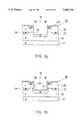
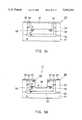
- FIG. 1ashows the cross section of a conventional vertical DMOS (VDMOS) transistor 10.
- VDMOSvertical DMOS
- a conventional VDMOS transistor 10has a N+ drain electrode 11 below a lightly doped N- region 12.
- N- region 12Within the N- region 12 is a pair of P-type regions 13a and 13b.
- Each of the P type regions 13a and 13brespectively has a N type source region, 15a and 15b.
- a polysilicon gate electrode 17is located above a portion of the N- region 12 overlapping both the P type regions 13a and 13b and the source electrodes 15a and 15b, with a dielectric layer 18 provided between the polysilicon gate electrode 17 and the aforementioned regions.
- a current 19is permitted to flow between the source electrodes and the drain electrode.
- the path of the currentis shown by arrows 19 and is both horizontal and vertical.
- FIG. 1bshows another type of conventional VDMOS transistor 20 which has a gate electrode 27 located in a trench. Current flows vertically from source electrodes 25a and 25b to a drain electrode 11 as shown by arrows 29.
- transistor 10consumes more electricity because the current 19 flows a longer distance in the lightly doped N- region 12, which results in a larger source/drain resistance.
- the transistor 20is more efficient because it has a shorter current path.
- both of the conventional VDMOS devices 10 and 20have a deficiency in that their source/drain resistances and breakdown voltages decrease when the doping density of their respective N- regions are increased. As a result, high breakdown voltage and low source/drain resistance can not be achieved simultaneously.
- a preferred methodcomprises the steps of: (a) forming a drain electrode region of the first conductivity type in the substrate, the drain electrode region having a drain electrode region doping density; (b) forming an epitaxial layer of the first conductivity type on the drain electrode region, the epitaxial layer having an epitaxial layer doping density less than the doping density of the drain electrode region; (c) forming a body region of a second conductivity type on the epitaxial layer; (d) forming a source electrode region of the first conductivity type in the body region; (e) forming a trench through the source electrode region and the body region, to reach the epitaxial layer; (f) implanting impurities of the first conductivity type into the bottom surface of the trench to form an implanted region having an implanted region doping density; (g) thermally diffusing the impurities in the step (f) and forming an oxide layer
- FIGS. 1a and 1bare cross sectional views of two kind of conventional vertical DMOS (VDMOS) transistors;
- FIGS. 2a to 2lare cross-sectional views of a first embodiment of the VDMOS transistor according to the present invention during various steps in its formation;
- FIGS. 3a to 3fare cross-sectional views of a second embodiment of the VDMOS transistor according to the present invention during various steps in its formation;
- FIGS. 4a to 4lare cross sectional views of a third embodiment of the VDMOS transistor according to the present invention during various steps in its formation.
- FIGS. 5a to 5fare cross-sectional views of a fourth embodiment of the VDMOS transistor according to the present invention during various stages in its formation.
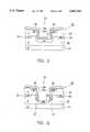
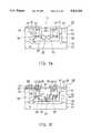
- FIGS. 2a to 2lThe fabrication of a transistor 30 according to a first embodiment of the present invention is illustrated in FIGS. 2a to 2l and described hereinafter.
- FIG. 2ashows a N+ substrate 31 which has a coefficient of electrical resistivity between 0.005 and 0.1 ⁇ -cm.
- a N-epitaxial layer 32 with a thickness from 8 to 100 ⁇ m and a coefficient of electrical resistivity between 0.1 and 100 ⁇ -cmis grown over the N+ substrate 31 by conventional epitaxial growth techniques.
- FIG. 2bshows an oxide layer 33a which is formed by thermally oxidizing the surface of the N- epitaxial layer 32.
- the oxide layer 33ais patterned using conventional lithographic techniques and boron (B 11 ) ions with a kinetic energy of 30 to 120 KeV are implanted into the N- epitaxial layer 32, to form P+ regions 34 with a dosage of 5 ⁇ 10 13 to 1 ⁇ 10 16 atoms/cm 2 .
- the oxide layer 33ais then removed by etching, as shown in FIG. 2c. Thereafter, boron (B 11 ) ions at 30 to 120 KeV with a dosage of 1 ⁇ 10 13 to 1 ⁇ 10 14 atoms/cm 2 are implanted into the upper surface of the N- epitaxial layer 32 to form a body region 35.
- the substrateis then heated and the body region 35 is diffused to a predetermined body region depth of 3 to 4 ⁇ m in the N- epitaxial layer 32 with another oxide layer 33b being simultaneously formed at the upper surface of the body region 35.
- the oxide layer 33bis then patterned using conventional lithographic techniques.
- Phosphorus (p 31 ) ions or arsenic (As 51 ) ions at 50 to 150 KeVare thereafter implanted into the body region 35 with a dosage of 1 ⁇ 10 15 to 1 ⁇ 10 16 atoms/cm 2 to form a source region 36 to a predetermined source region depth which is less than the predetermined body region depth of 3-4 ⁇ m.
- FIG. 2eshows that the source region 36 is then thermally diffused into the body region 35 with an oxide layer having a thickness of 1 to 2 ⁇ m being simultaneously formed thereon.
- a trench 70is thereafter formed by conventional lithographic techniques using a trench mask and reactive ion etching (RIE) to etch to a predetermined first trench depth of 4 to 5 ⁇ m into the N- epitaxial layer 32 as shown in FIG. 2f.
- RIEreactive ion etching
- FIG. 2gshows that phosphorous (p 31 ) ions or arsenic (As 51 ) ions are then implanted into the bottom of the trench 70, to form a first N type implanted region 37.
- the substrateis thereafter heated to grow a first gate oxide layer 33c and to drive the phosphorus or arsenic ions into the bottom of the trench as shown in FIG. 2h.
- the substrateis then annealed.
- the doping density of the first N type implanted region 37is higher than the doping density of the N- epitaxial layer 32.
- FIG. 2ishows a silicon nitride layer 38 which is then deposited on the gate oxide layer 33c by chemical vapor deposition (CVD ).
- the bottom of the trench 70is again etched by RIE (effectively creating a narrower and deeper second trench within the original trench 70) and then phosphorus (p 31 ) ions or arsenic (As 51 ) ions are again implanted into the bottom of the trench 70 to form a second N type implanted region 39.
- the doping density of the second N type implanted region 39is higher than the doping density of the first N type implanted region 37.
- the doping density of the second N type implanted region 39is lower than the doping density of the N+ substrate 31.
- the substrateis then heated to form a second gate oxide layer 33d while simultaneously diffusing the phosphorus or arsenic ions in the second N type implanted region 39.
- the thickness of the second gate oxide layer 33dis greater than the thickness of the first gate oxide layer 33c.
- FIG. 21shows a poly gate 40 which is formed in the trench 70 by depositing polysilicon on the substrate and then etching the portion of polysilicon that is not in the trench 70.
- An oxide layer 41is thereafter formed by CVD on the substrate. Then metal vias and metal contacts and wiring are formed by conventional lithographic techniques.
- the source/drain resistanceis reduced when the doping density is increased in the current flow path.
- the doping density in the current flow pathis always N-.
- the relationship of the doping density in the current flow path in different areas of the transistoris:
- N-is the doping density of the N- epitaxial layer
- N 1is the doping density of the first N-type implanted region
- N 2is the doping density of the second N-type implanted region
- N+is the doping density of the N+ substrate. Accordingly, the source/drain resistance of the present invention is lower than that of prior art VDMOS transistors.
- the conventional decrease in the breakdown voltagewhich is associated with a reduction in the source/drain resistance, is prevented by increasing the thickness of the gate oxide layer.
- an increase in the thickness of the gate oxide layerprevents the above-described decrease in the breakdown voltage.
- the VDMOS transistor of the first embodimentdoes not experience the conventional reduction in a breakdown voltage where the doping density is increased because the doping density of the second N type implanted region 39 is higher than the doping density of the first N type implanted region 37, and thickness of the gate oxide layer on the second N type implanted region 39 is greater than that of the first N type implanted region 37.
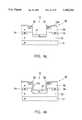
- FIGS. 3a to 3fThe fabrication of a transistor 50 according to a second embodiment of the present invention is illustrated in FIGS. 3a to 3f and described hereinafter.
- FIG. 3ashows the implantation of N type impurities into a P type substrate 51 to form a N+ type buried layer 52.
- a N- epitaxial layer 53 with a thickness from 8 to 100 ⁇ mis thereafter grown on the P type substrate 51.
- FIG. 3cillustrates that N type impurities are then implanted into the N-epitaxial layer 53 at a predetermined sinker position to form a sinker 54 in connection with the buried layer 52.
- the sinker 54functions as a drain electrode.
- the buried layer 52 and the sinker 54define an active region within which a VDMOS transistor may be built. The following steps are similar to the corresponding process of the first embodiment.
- An oxide mask layer 55is first formed, patterned and then boron (B 11 ) ions are implanted with a dosage between 5 ⁇ 10 13 to 1 ⁇ 10 16 atoms/cm 2 at a predetermined implantation region position to form a P+ region 56.
- boron ionsare implanted into the active region with a dosage of 1 ⁇ 10 13 to 1 ⁇ 10 14 atoms/cm 2 to form a P type body region 57.
- a source electrode 58is then formed by removing a portion of the oxide layer on the source electrode 58 using a conventional lithographic technique and implanting phosphorus (p 31 ) ions or arsenic ions into the body region 57 with a dosage of 1 ⁇ 10 15 to 1 ⁇ 10 16 atoms/cm 2 .
- the substrateis again heated to diffuse the source electrode 58 to a depth of 1 to 2 ⁇ m in the body region 57 and an oxide layer is grown on the source electrode 58.
- a trench 71is then formed by conventional lithographic techniques using a trench mask and RIE to etch into the N- epitaxial layer 53. Thereafter, phosphorus (p 31 ) ions or arsenic ions are implanted into the bottom of the trench 71 to form a first N type implanted region 59.
- the doping density of the first N type implanted region 59is higher than the doping density of the N- epitaxial layer 53.
- the substrateis then heated to grow a first gate oxide layer 60 and to drive in the phosphorus or arsenic ions.
- the substrateis then annealed.
- a silicon nitride layer 61is thereafter deposited on the gate oxide layer 60 by chemical vapor deposition (CVD).
- CVDchemical vapor deposition
- the bottom of the trench 71is further deepened using RIE, and then implanted with phosphorus (p 31 ) ions or arsenic (As 51 ) ions to form a second N type implanted region 62.
- the doping density of the second N type implanted region 62is higher than the doping density of the first N type implanted region 59.
- the doping density of the second N type implanted region 62is lower than the doping density of the N+ substrate 51.
- FIG. 3fshows that the substrate is then heated to form a second gate oxide layer 63 with phosphorus or arsenic ions in the second N type implanted region 62 being simultaneously diffused further into the substrate.
- the thickness of the second gate oxide layer 63is greater than the thickness of the first gate oxide layer 60.
- a poly gate 64is formed in the trench 71 by depositing polysilicon on the substrate and then etching the portion of polysilicon that is not in the trench 71.
- An oxide layer 65is then formed by CVD on the substrate.
- metal vias, metal contacts and wiringare formed by conventional lithographic techniques.
- N type impuritiesare implanted into the bottom of the trench twice to form two N type implanted regions. Even better performance may be achieved by forming more than two N type implanted regions. In that case, the relation between each implanted region is:
- N-is the doping density of the N- epitaxial layer
- N 1is the doping density of the first N-type implanted region
- N 2is the doping density of the second N-type implanted region
- N nis the doping density of an n-th N-type implanted region
- N+is the doping density of the N+ substrate.
- the thickness of the corresponding gate oxide layersmay be increased to compensate for the reduction in breakdown voltage which is conventionally associated with increased doping densities.
- the relationship between the gate oxide thicknesses corresponding to the respective implanted regionsis:
- T ox ,N1is the thickness of the gate oxide layer of the first N-type implanted region
- T ox ,N2is the thickness of the gate oxide layer of the second N-type implanted region
- T ox ,N3is the thickness of the gate oxide layer of the third N-type implanted region.
- T ox ,Nnis the thickness of the gate oxide layer of an n-th N-type implanted region.
- the minimum width of the trenchmust be increased as the number of implanted regions in the trench is increased. Furthermore, whether or not the drain electrode is electrically connected to the implanted region which is closest to the drain electrode has no effect on the advantages provided by the present invention. For example, the second implanted region 39 in the first embodiment is not connected with the drain electrode.
- D-is the doping density of the D- epitaxial layer:
- D 1is the doping density of the first D-type implanted region:
- D 2is the doping density of the second D-type implanted region
- D nis the doping density of the n-th D-type implanted region
- D+is the doping density of the D+ substrate.
- the relationship between the gate oxide thicknesses corresponding to the respective implanted regionsmay be more generally stated as:
- T ox ,D1is the thickness of the gate oxide layer of the first D-type implanted region
- T ox ,D 2is the thickness of the gate oxide layer of the second D-type implanted region
- T ox ,D 3is the thickness of the gate oxide layer of the third D-type implanted region.
- T ox ,D nis the thickness of the gate oxide layer of the n-th D-type implanted region.
Landscapes
- Metal-Oxide And Bipolar Metal-Oxide Semiconductor Integrated Circuits (AREA)
- Insulated Gate Type Field-Effect Transistor (AREA)
Abstract
Description
This is a divisional of co-pending application Ser. No. 08/287,950 filed Aug. 9, 1994.
The present invention relates to double diffused metal-oxide-semiconductor (DMOS) transistors, and in particular to a vertical DMOS transistor having a lower drain-source resistance and method of forming the same.
FIG. 1a shows the cross section of a conventional vertical DMOS (VDMOS)transistor 10. Aconventional VDMOS transistor 10 has aN+ drain electrode 11 below a lightly doped N-region 12. Within the N-region 12 is a pair of P-type regions P type regions polysilicon gate electrode 17 is located above a portion of the N-region 12 overlapping both theP type regions source electrodes dielectric layer 18 provided between thepolysilicon gate electrode 17 and the aforementioned regions. When thedrain electrode 11 is grounded and the voltage at thesource electrodes arrows 19 and is both horizontal and vertical.
FIG. 1b shows another type ofconventional VDMOS transistor 20 which has agate electrode 27 located in a trench. Current flows vertically fromsource electrodes drain electrode 11 as shown byarrows 29.
Comparing the above-describedconventional VDMOS transistors transistor 10 consumes more electricity because the current 19 flows a longer distance in the lightly doped N-region 12, which results in a larger source/drain resistance. As may be readily appreciated, thetransistor 20 is more efficient because it has a shorter current path. Although the trenched structure oftransistor 20 reduces the source/drain resistance, both of theconventional VDMOS devices
It is therefore an object for the present invention to reduce the source/drain resistance of VDMOS transistors while maintaining a high breakdown voltage.
The object of the present invention is fulfilled by providing a method for fabricating a VDMOS transistor on a substrate of a first conductivity type. A preferred method comprises the steps of: (a) forming a drain electrode region of the first conductivity type in the substrate, the drain electrode region having a drain electrode region doping density; (b) forming an epitaxial layer of the first conductivity type on the drain electrode region, the epitaxial layer having an epitaxial layer doping density less than the doping density of the drain electrode region; (c) forming a body region of a second conductivity type on the epitaxial layer; (d) forming a source electrode region of the first conductivity type in the body region; (e) forming a trench through the source electrode region and the body region, to reach the epitaxial layer; (f) implanting impurities of the first conductivity type into the bottom surface of the trench to form an implanted region having an implanted region doping density; (g) thermally diffusing the impurities in the step (f) and forming an oxide layer in the trench; (h) forming a silicon nitride layer on the oxide layer in the step (g); (i) etching the bottom of the trench to reach the epitaxial layer; (j) implanting impurities of the first conductivity type into the bottom of the trench to form another implanted region having a doping density larger than the doping density of the implanted region in the step (f); (k) thermally diffusing the impurities in the step (j) and forming an oxide layer on the bottom of the trench; (l) repeating the steps (i) to (k) with a continuously increased doping density of the implanted region in the step (j) at least once; (m) forming a gate electrode in the trench; (n) forming another oxide layer on the substrate; (o) forming predetermined metal vias in the oxide layer of the step (n); and (p) forming predetermined metal contacts and wiring.
The present invention is more fully understood from the detailed description provided hereinafter with reference to the accompanying drawings which are given by way of illustration only, and thus not limitative of the present invention and wherein:
FIGS. 1a and 1b are cross sectional views of two kind of conventional vertical DMOS (VDMOS) transistors;
FIGS. 2a to 2l are cross-sectional views of a first embodiment of the VDMOS transistor according to the present invention during various steps in its formation;
FIGS. 3a to 3f are cross-sectional views of a second embodiment of the VDMOS transistor according to the present invention during various steps in its formation;
FIGS. 4a to 4l are cross sectional views of a third embodiment of the VDMOS transistor according to the present invention during various steps in its formation; and
FIGS. 5a to 5f are cross-sectional views of a fourth embodiment of the VDMOS transistor according to the present invention during various stages in its formation.
The fabrication of atransistor 30 according to a first embodiment of the present invention is illustrated in FIGS. 2a to 2l and described hereinafter.
Step 1
FIG. 2a shows aN+ substrate 31 which has a coefficient of electrical resistivity between 0.005 and 0.1 Ω-cm. A N-epitaxial layer 32 with a thickness from 8 to 100 μm and a coefficient of electrical resistivity between 0.1 and 100 Ω-cm is grown over theN+ substrate 31 by conventional epitaxial growth techniques.
Step 2
FIG. 2b shows anoxide layer 33a which is formed by thermally oxidizing the surface of the N-epitaxial layer 32. Next, theoxide layer 33a is patterned using conventional lithographic techniques and boron (B11) ions with a kinetic energy of 30 to 120 KeV are implanted into the N-epitaxial layer 32, to formP+ regions 34 with a dosage of 5×10¹³ to 1×10¹⁶ atoms/cm2.
Step 3
Theoxide layer 33a is then removed by etching, as shown in FIG. 2c. Thereafter, boron (B11) ions at 30 to 120 KeV with a dosage of 1×10¹³ to 1×10¹⁴ atoms/cm2 are implanted into the upper surface of the N-epitaxial layer 32 to form abody region 35. The substrate is then heated and thebody region 35 is diffused to a predetermined body region depth of 3 to 4 μm in the N-epitaxial layer 32 with anotheroxide layer 33b being simultaneously formed at the upper surface of thebody region 35.
Step 4
As is shown in FIG. 2d, theoxide layer 33b is then patterned using conventional lithographic techniques. Phosphorus (p31) ions or arsenic (As51) ions at 50 to 150 KeV are thereafter implanted into thebody region 35 with a dosage of 1×10¹⁵ to 1×10¹⁶ atoms/cm2 to form asource region 36 to a predetermined source region depth which is less than the predetermined body region depth of 3-4 μm.
Step 5
FIG. 2e shows that thesource region 36 is then thermally diffused into thebody region 35 with an oxide layer having a thickness of 1 to 2 μm being simultaneously formed thereon.
Step 6
Atrench 70 is thereafter formed by conventional lithographic techniques using a trench mask and reactive ion etching (RIE) to etch to a predetermined first trench depth of 4 to 5 μm into the N-epitaxial layer 32 as shown in FIG. 2f.
Step 7
FIG. 2g shows that phosphorous (p31) ions or arsenic (As51) ions are then implanted into the bottom of thetrench 70, to form a first N type implantedregion 37. The substrate is thereafter heated to grow a firstgate oxide layer 33c and to drive the phosphorus or arsenic ions into the bottom of the trench as shown in FIG. 2h. The substrate is then annealed. The doping density of the first N type implantedregion 37 is higher than the doping density of the N-epitaxial layer 32.
Step 8
FIG. 2i shows asilicon nitride layer 38 which is then deposited on thegate oxide layer 33c by chemical vapor deposition (CVD ).
Step 9
As shown in FIG. 2j, the bottom of thetrench 70 is again etched by RIE (effectively creating a narrower and deeper second trench within the original trench 70) and then phosphorus (p31) ions or arsenic (As51) ions are again implanted into the bottom of thetrench 70 to form a second N type implantedregion 39. The doping density of the second N type implantedregion 39 is higher than the doping density of the first N type implantedregion 37. The doping density of the second N type implantedregion 39 is lower than the doping density of theN+ substrate 31.
The substrate is then heated to form a secondgate oxide layer 33d while simultaneously diffusing the phosphorus or arsenic ions in the second N type implantedregion 39. The thickness of the secondgate oxide layer 33d, as is best illustrated in FIG. 2k, is greater than the thickness of the firstgate oxide layer 33c.
Finally, FIG. 21 shows apoly gate 40 which is formed in thetrench 70 by depositing polysilicon on the substrate and then etching the portion of polysilicon that is not in thetrench 70. Anoxide layer 41 is thereafter formed by CVD on the substrate. Then metal vias and metal contacts and wiring are formed by conventional lithographic techniques.
As discussed previously, the source/drain resistance is reduced when the doping density is increased in the current flow path. In a conventional VDMOS transistor, the doping density in the current flow path is always N-. In the VDMOS transistor according to the present invention, the relationship of the doping density in the current flow path in different areas of the transistor is:
N-<N.sub.1 <N.sub.2 <N+
wherein:
N- is the doping density of the N- epitaxial layer;
N1 is the doping density of the first N-type implanted region;
N2 is the doping density of the second N-type implanted region; and
N+ is the doping density of the N+ substrate. Accordingly, the source/drain resistance of the present invention is lower than that of prior art VDMOS transistors.
Furthermore, the conventional decrease in the breakdown voltage, which is associated with a reduction in the source/drain resistance, is prevented by increasing the thickness of the gate oxide layer. In particular, it has been observed that as the doping density increases, an increase in the thickness of the gate oxide layer prevents the above-described decrease in the breakdown voltage. In summary, the VDMOS transistor of the first embodiment does not experience the conventional reduction in a breakdown voltage where the doping density is increased because the doping density of the second N type implantedregion 39 is higher than the doping density of the first N type implantedregion 37, and thickness of the gate oxide layer on the second N type implantedregion 39 is greater than that of the first N type implantedregion 37.
The fabrication of atransistor 50 according to a second embodiment of the present invention is illustrated in FIGS. 3a to 3f and described hereinafter.
Step 1
FIG. 3a shows the implantation of N type impurities into aP type substrate 51 to form a N+ type buriedlayer 52.
Step 2
As shown in FIG. 3b, a N-epitaxial layer 53 with a thickness from 8 to 100 μm is thereafter grown on theP type substrate 51.
Step 3
FIG. 3c illustrates that N type impurities are then implanted into the N-epitaxial layer 53 at a predetermined sinker position to form asinker 54 in connection with the buriedlayer 52. Thesinker 54 functions as a drain electrode. The buriedlayer 52 and thesinker 54 define an active region within which a VDMOS transistor may be built. The following steps are similar to the corresponding process of the first embodiment.
Anoxide mask layer 55 is first formed, patterned and then boron (B11) ions are implanted with a dosage between 5×10¹³ to 1×10¹⁶ atoms/cm2 at a predetermined implantation region position to form aP+ region 56. Next, a portion of the oxide layer on the active region is etched, and boron ions are implanted into the active region with a dosage of 1×10¹³ to 1×10¹⁴ atoms/cm2 to form a Ptype body region 57.
Step 4
The substrate is then heated and thebody region 57 is diffused to a depth of 3 to 4 μm in the N-epitaxial layer 53 with anotheroxide layer 55 being formed simultaneously. As is shown in FIG. 3d, asource electrode 58 is then formed by removing a portion of the oxide layer on thesource electrode 58 using a conventional lithographic technique and implanting phosphorus (p31) ions or arsenic ions into thebody region 57 with a dosage of 1×10¹⁵ to 1×10¹⁶ atoms/cm2. The substrate is again heated to diffuse thesource electrode 58 to a depth of 1 to 2 μm in thebody region 57 and an oxide layer is grown on thesource electrode 58. Atrench 71 is then formed by conventional lithographic techniques using a trench mask and RIE to etch into the N-epitaxial layer 53. Thereafter, phosphorus (p31) ions or arsenic ions are implanted into the bottom of thetrench 71 to form a first N type implantedregion 59. The doping density of the first N type implantedregion 59 is higher than the doping density of the N-epitaxial layer 53.
Step 5
As is shown in FIG. 3e, the substrate is then heated to grow a firstgate oxide layer 60 and to drive in the phosphorus or arsenic ions. The substrate is then annealed. Asilicon nitride layer 61 is thereafter deposited on thegate oxide layer 60 by chemical vapor deposition (CVD). After the aforementioned steps, the bottom of thetrench 71 is further deepened using RIE, and then implanted with phosphorus (p31) ions or arsenic (As51) ions to form a second N type implantedregion 62. The doping density of the second N type implantedregion 62 is higher than the doping density of the first N type implantedregion 59. The doping density of the second N type implantedregion 62 is lower than the doping density of theN+ substrate 51.
Step 6
FIG. 3f shows that the substrate is then heated to form a secondgate oxide layer 63 with phosphorus or arsenic ions in the second N type implantedregion 62 being simultaneously diffused further into the substrate. The thickness of the secondgate oxide layer 63 is greater than the thickness of the firstgate oxide layer 60. Next, apoly gate 64 is formed in thetrench 71 by depositing polysilicon on the substrate and then etching the portion of polysilicon that is not in thetrench 71. Anoxide layer 65 is then formed by CVD on the substrate. Lastly, metal vias, metal contacts and wiring are formed by conventional lithographic techniques.
The advantages of the second embodiment are similar to those of the first embodiment, and therefore are not repeated here.
In the first and second embodiments, N type impurities are implanted into the bottom of the trench twice to form two N type implanted regions. Even better performance may be achieved by forming more than two N type implanted regions. In that case, the relation between each implanted region is:
N-<N.sub.1 <N.sub.2 <. . . <N.sub.n <N+
wherein:
N-is the doping density of the N- epitaxial layer;
N1 is the doping density of the first N-type implanted region;
N2 is the doping density of the second N-type implanted region;
Nn is the doping density of an n-th N-type implanted region; and
N+ is the doping density of the N+ substrate.
Although successively increasing densities of the respective implanted regions lower the source/drain resistance, the thickness of the corresponding gate oxide layers may be increased to compensate for the reduction in breakdown voltage which is conventionally associated with increased doping densities. The relationship between the gate oxide thicknesses corresponding to the respective implanted regions is:
T.sub.ox,N1 <T.sub.ox,N2 <T.sub.ox,N3 <. . . <T.sub.ox,Nn
wherein:
Tox,N1 is the thickness of the gate oxide layer of the first N-type implanted region;
Tox,N2 is the thickness of the gate oxide layer of the second N-type implanted region;
Tox,N3 is the thickness of the gate oxide layer of the third N-type implanted region; and
Tox,Nn is the thickness of the gate oxide layer of an n-th N-type implanted region.
As may be readily appreciated, the minimum width of the trench must be increased as the number of implanted regions in the trench is increased. Furthermore, whether or not the drain electrode is electrically connected to the implanted region which is closest to the drain electrode has no effect on the advantages provided by the present invention. For example, the second implantedregion 39 in the first embodiment is not connected with the drain electrode.
It should be also noted that the present invention is applicable to either PMOS or NMOS as shown in FIGS. 4a to 4l and FIGS. 5a to 5f. Since the interchange of P type and N type is well known to those skilled in the art, it is not further .discussed hereinafter, except and insofar as the foregoing relationships are equally applicable to both P type and N type. Ergo, the relation between the doping densities of each implanted region may be more generally described as:
D-<D.sub.1 <D.sub.2 <. . . <D.sub.n <D+
wherein:
D- is the doping density of the D- epitaxial layer:
D1 is the doping density of the first D-type implanted region:
D2 is the doping density of the second D-type implanted region;
Dn is the doping density of the n-th D-type implanted region; and
D+ is the doping density of the D+ substrate.
Similarly, the relationship between the gate oxide thicknesses corresponding to the respective implanted regions may be more generally stated as:
T.sub.ox,D1 <T.sub.ox,D2 <T.sub.ox,D3 <. . . <T.sub.ox,Dn
wherein:
Tox,D1 is the thickness of the gate oxide layer of the first D-type implanted region;
Tox,D2 is the thickness of the gate oxide layer of the second D-type implanted region;
Tox,D3 is the thickness of the gate oxide layer of the third D-type implanted region; and
Tox,Dn is the thickness of the gate oxide layer of the n-th D-type implanted region.
While the invention has been described by way of examples and in terms of several preferred embodiments, it is to be understood that the invention need not be limited to the disclosed embodiments. On the contrary, the disclosed invention is intended to cover various modifications and similar arrangements within the spirit and scope of the appended claims, the scope of which should be accorded the broadest interpretation so as to encompass all such modifications and similar structures.
Claims (5)
1. A VDMOS transistor on a semiconductor substrate, comprising:
a drain electrode region of a first conductivity type in said substrate, said drain electrode region having a drain electrode region doping density (D+);
an epitaxial layer of said first conductivity type formed on said drain electrode region, said epitaxial layer having an epitaxial layer doping density (D-), said epitaxial layer defining a first trench and a deeper and narrower second trench within said first trench, said epitaxial layer including a first implanted region of said first conductivity type adjoining said first trench and a second implanted region of said first conductivity type adjoining said second trench, said first and said second implanted regions having a first and a second implanted region doping density (D1), (D2), respectively;
a first gate oxide layer formed within said first trench adjacent to said first implanted region, said first gate oxide layer having a first gate oxide layer thickness (TOX,D1); and
a second gate oxide layer formed within said second trench adjacent to said second implanted region, said second gate oxide layer having a second gate oxide layer thickness (TOX,D2), wherein:
D-<D.sub.1 <D.sub.2 <D+;
and
T.sub.OX,D1 <T.sub.OX,D2.
2. The VDMOS transistor of claim 1, wherein said first conductivity type is N type.
3. The VDMOS transistor of claim 1, wherein said first conductivity type is P type.
4. The VDMOS transistor of claim 1, wherein said drain electrode region has a coefficient of drain electrode region electrical resistance between 0.005 and 0.1 Ω-cm.
5. The VDMOS transistor of claim 1, wherein said epitaxial layer has a coefficient of epitaxial layer electrical resistance between 0.1 and 100 Ω-cm and an epitaxial layer thickness between 8 and 100 μm.
Priority Applications (1)
| Application Number | Priority Date | Filing Date | Title |
|---|---|---|---|
| US08/330,567US5442214A (en) | 1994-08-09 | 1994-10-28 | VDMOS transistor and manufacturing method therefor |
Applications Claiming Priority (2)
| Application Number | Priority Date | Filing Date | Title |
|---|---|---|---|
| US08/287,950US5424231A (en) | 1994-08-09 | 1994-08-09 | Method for manufacturing a VDMOS transistor |
| US08/330,567US5442214A (en) | 1994-08-09 | 1994-10-28 | VDMOS transistor and manufacturing method therefor |
Related Parent Applications (1)
| Application Number | Title | Priority Date | Filing Date |
|---|---|---|---|
| US08/287,950DivisionUS5424231A (en) | 1994-08-09 | 1994-08-09 | Method for manufacturing a VDMOS transistor |
Publications (1)
| Publication Number | Publication Date |
|---|---|
| US5442214Atrue US5442214A (en) | 1995-08-15 |
Family
ID=23105081
Family Applications (2)
| Application Number | Title | Priority Date | Filing Date |
|---|---|---|---|
| US08/287,950Expired - Fee RelatedUS5424231A (en) | 1994-08-09 | 1994-08-09 | Method for manufacturing a VDMOS transistor |
| US08/330,567Expired - Fee RelatedUS5442214A (en) | 1994-08-09 | 1994-10-28 | VDMOS transistor and manufacturing method therefor |
Family Applications Before (1)
| Application Number | Title | Priority Date | Filing Date |
|---|---|---|---|
| US08/287,950Expired - Fee RelatedUS5424231A (en) | 1994-08-09 | 1994-08-09 | Method for manufacturing a VDMOS transistor |
Country Status (1)
| Country | Link |
|---|---|
| US (2) | US5424231A (en) |
Cited By (78)
| Publication number | Priority date | Publication date | Assignee | Title |
|---|---|---|---|---|
| US5488244A (en)* | 1995-02-27 | 1996-01-30 | Chartered Simiconductor Manufacturing Pte Ltd. | Electrically erasable and programmable read only memory cell |
| US5670803A (en)* | 1995-02-08 | 1997-09-23 | International Business Machines Corporation | Three-dimensional SRAM trench structure and fabrication method therefor |
| WO1998004004A1 (en)* | 1996-07-19 | 1998-01-29 | Siliconix Incorporated | High density trench dmos transistor with trench bottom implant |
| US5877538A (en)* | 1995-06-02 | 1999-03-02 | Silixonix Incorporated | Bidirectional trench gated power MOSFET with submerged body bus extending underneath gate trench |
| US5886382A (en)* | 1997-07-18 | 1999-03-23 | Motorola, Inc. | Trench transistor structure comprising at least two vertical transistors |
| US5930651A (en)* | 1994-04-28 | 1999-07-27 | Ngk Insulators, Ltd. | Method of forming a semiconductor device having a plurality of cavity defined gating regions |
| US6069385A (en)* | 1995-06-07 | 2000-05-30 | Stmicroelectronics, Inc. | Trench MOS-gated device |
| US6096608A (en)* | 1997-06-30 | 2000-08-01 | Siliconix Incorporated | Bidirectional trench gated power mosfet with submerged body bus extending underneath gate trench |
| US6204123B1 (en) | 1998-10-30 | 2001-03-20 | Sony Corporation | Vertical floating gate transistor with epitaxial channel |
| US6218228B1 (en)* | 1995-03-31 | 2001-04-17 | Consorzio Per La Ricerca Sulla Microelettronica Nel Mezzogiorno | DMOS device structure, and related manufacturing process |
| US6262453B1 (en)* | 1998-04-24 | 2001-07-17 | Magepower Semiconductor Corp. | Double gate-oxide for reducing gate-drain capacitance in trenched DMOS with high-dopant concentration buried-region under trenched gate |
| US6285059B1 (en)* | 1999-03-18 | 2001-09-04 | United Microelectronics Corp. | Structure for laterally diffused metal-oxide semiconductor |
| US6433385B1 (en)* | 1999-05-19 | 2002-08-13 | Fairchild Semiconductor Corporation | MOS-gated power device having segmented trench and extended doping zone and process for forming same |
| US6469345B2 (en)* | 2000-01-14 | 2002-10-22 | Denso Corporation | Semiconductor device and method for manufacturing the same |
| US20030030104A1 (en)* | 2001-08-10 | 2003-02-13 | Darwish Mohamed N. | Trench MIS device with graduated gate oxide layer |
| WO2003044865A1 (en)* | 2001-11-15 | 2003-05-30 | General Semiconductor, Inc. | Trench mosfet having low gate charge |
| WO2003046997A1 (en)* | 2001-11-21 | 2003-06-05 | General Semiconductor, Inc. | Trench mosfet device with improved on-resistance |
| US6664163B2 (en) | 1997-12-05 | 2003-12-16 | Naoto Fujishima | Low on-resistance trench lateral MISFET with better switching characteristics and method for manufacturing same |
| US6696726B1 (en)* | 2000-08-16 | 2004-02-24 | Fairchild Semiconductor Corporation | Vertical MOSFET with ultra-low resistance and low gate charge |
| US20040038481A1 (en)* | 2001-07-03 | 2004-02-26 | Siliconix Incorporated | Trench MOSFET having implanted drain-drift region and process for manufacturing the same |
| US20040038467A1 (en)* | 2001-07-03 | 2004-02-26 | Siliconix Incorporated | Trench MIS device having implanted drain-drift region and thick bottom oxide and process for manufacturing the same |
| US6710418B1 (en) | 2002-10-11 | 2004-03-23 | Fairchild Semiconductor Corporation | Schottky rectifier with insulation-filled trenches and method of forming the same |
| US6710403B2 (en) | 2002-07-30 | 2004-03-23 | Fairchild Semiconductor Corporation | Dual trench power MOSFET |
| US20040065920A1 (en)* | 2002-06-28 | 2004-04-08 | Timothy Henson | Short channel trench mosfet with reduced gate charge |
| US20040065919A1 (en)* | 2002-10-03 | 2004-04-08 | Wilson Peter H. | Trench gate laterally diffused MOSFET devices and methods for making such devices |
| US20040082140A1 (en)* | 2002-10-25 | 2004-04-29 | Jia-Wei Yang | Deep trench isolation structure of a high-voltage device and method for forming thereof |
| US20040121572A1 (en)* | 2001-07-03 | 2004-06-24 | Darwish Mohamed N. | Trench MIS device having implanted drain-drift region and thick bottom oxide and process for manufacturing the same |
| US20040166636A1 (en)* | 2001-07-03 | 2004-08-26 | Siliconix Incorporated | Trench MIS device with thick oxide layer in bottom of gate contact trench |
| US20040171220A1 (en)* | 2002-10-25 | 2004-09-02 | Vanguard International Semiconductor Corporation | Fabrication method for a deep trench isolation structure of a high-voltage device |
| US6803626B2 (en) | 2002-07-18 | 2004-10-12 | Fairchild Semiconductor Corporation | Vertical charge control semiconductor device |
| US6864532B2 (en) | 2000-01-14 | 2005-03-08 | Denso Corporation | Semiconductor device and method for manufacturing the same |
| US20050104093A1 (en)* | 2003-11-17 | 2005-05-19 | Kenichi Yoshimochi | Semiconductor device and method for fabricating the same |
| US6916745B2 (en) | 2003-05-20 | 2005-07-12 | Fairchild Semiconductor Corporation | Structure and method for forming a trench MOSFET having self-aligned features |
| US20050215011A1 (en)* | 2004-03-26 | 2005-09-29 | Siliconix Incorporated | Termination for trench MIS device having implanted drain-drift region |
| US6991977B2 (en) | 2001-10-17 | 2006-01-31 | Fairchild Semiconductor Corporation | Method for forming a semiconductor structure with improved smaller forward voltage loss and higher blocking capability |
| US20060038223A1 (en)* | 2001-07-03 | 2006-02-23 | Siliconix Incorporated | Trench MOSFET having drain-drift region comprising stack of implanted regions |
| US7061066B2 (en) | 2001-10-17 | 2006-06-13 | Fairchild Semiconductor Corporation | Schottky diode using charge balance structure |
| US7132712B2 (en) | 2002-11-05 | 2006-11-07 | Fairchild Semiconductor Corporation | Trench structure having one or more diodes embedded therein adjacent a PN junction |
| US20060255402A1 (en)* | 2005-05-12 | 2006-11-16 | M-Mos Sdn. Bhd. | Elimination of gate oxide weak spot in deep trench |
| US20070190714A1 (en)* | 2003-12-23 | 2007-08-16 | Infineon Technologies Ag | Trench transistor and method for fabricating a trench transistor with high-energy-implanted drain |
| US7265416B2 (en) | 2002-02-23 | 2007-09-04 | Fairchild Korea Semiconductor Ltd. | High breakdown voltage low on-resistance lateral DMOS transistor |
| US7265415B2 (en) | 2004-10-08 | 2007-09-04 | Fairchild Semiconductor Corporation | MOS-gated transistor with reduced miller capacitance |
| US7301203B2 (en) | 2003-11-28 | 2007-11-27 | Fairchild Korea Semiconductor Ltd. | Superjunction semiconductor device |
| US7319256B1 (en) | 2006-06-19 | 2008-01-15 | Fairchild Semiconductor Corporation | Shielded gate trench FET with the shield and gate electrodes being connected together |
| US7345342B2 (en) | 2001-01-30 | 2008-03-18 | Fairchild Semiconductor Corporation | Power semiconductor devices and methods of manufacture |
| US7352036B2 (en) | 2004-08-03 | 2008-04-01 | Fairchild Semiconductor Corporation | Semiconductor power device having a top-side drain using a sinker trench |
| US7368777B2 (en) | 2003-12-30 | 2008-05-06 | Fairchild Semiconductor Corporation | Accumulation device with charge balance structure and method of forming the same |
| US7385248B2 (en) | 2005-08-09 | 2008-06-10 | Fairchild Semiconductor Corporation | Shielded gate field effect transistor with improved inter-poly dielectric |
| DE10312911B4 (en)* | 2003-03-22 | 2008-09-25 | Infineon Technologies Ag | Semiconductor component with space-saving edge termination |
| US7446374B2 (en) | 2006-03-24 | 2008-11-04 | Fairchild Semiconductor Corporation | High density trench FET with integrated Schottky diode and method of manufacture |
| US7504306B2 (en) | 2005-04-06 | 2009-03-17 | Fairchild Semiconductor Corporation | Method of forming trench gate field effect transistor with recessed mesas |
| US20090140329A1 (en)* | 2007-11-14 | 2009-06-04 | Rohm Co. Ltd. | Semiconductor Device |
| US7576388B1 (en) | 2002-10-03 | 2009-08-18 | Fairchild Semiconductor Corporation | Trench-gate LDMOS structures |
| US7625793B2 (en) | 1999-12-20 | 2009-12-01 | Fairchild Semiconductor Corporation | Power MOS device with improved gate charge performance |
| US7638841B2 (en) | 2003-05-20 | 2009-12-29 | Fairchild Semiconductor Corporation | Power semiconductor devices and methods of manufacture |
| US20100013009A1 (en)* | 2007-12-14 | 2010-01-21 | James Pan | Structure and Method for Forming Trench Gate Transistors with Low Gate Resistance |
| US7745289B2 (en) | 2000-08-16 | 2010-06-29 | Fairchild Semiconductor Corporation | Method of forming a FET having ultra-low on-resistance and low gate charge |
| US20100176444A1 (en)* | 2009-01-09 | 2010-07-15 | Niko Semiconductor Co., Ltd. | Power mosfet and method of fabricating the same |
| US7772668B2 (en) | 2007-12-26 | 2010-08-10 | Fairchild Semiconductor Corporation | Shielded gate trench FET with multiple channels |
| US20120056247A1 (en)* | 2010-09-08 | 2012-03-08 | Donghua Liu | Pseudo buried layer and manufacturing method of the same, deep hole contact and bipolar transistor |
| CN102456580A (en)* | 2010-10-25 | 2012-05-16 | 韩国电子通信研究院 | Semiconductor device and manufacturing method thereof |
| US8319290B2 (en) | 2010-06-18 | 2012-11-27 | Fairchild Semiconductor Corporation | Trench MOS barrier schottky rectifier with a planar surface using CMP techniques |
| US8426275B2 (en)* | 2009-01-09 | 2013-04-23 | Niko Semiconductor Co., Ltd. | Fabrication method of trenched power MOSFET |
| CN103187303A (en)* | 2011-12-27 | 2013-07-03 | 茂达电子股份有限公司 | Method for manufacturing power semiconductor device |
| US8673700B2 (en) | 2011-04-27 | 2014-03-18 | Fairchild Semiconductor Corporation | Superjunction structures for power devices and methods of manufacture |
| US20140145258A1 (en)* | 2012-11-23 | 2014-05-29 | Anpec Electronics Corporation | Semiconductor device with reduced miller capacitance and fabrication method thereof |
| US8772868B2 (en) | 2011-04-27 | 2014-07-08 | Fairchild Semiconductor Corporation | Superjunction structures for power devices and methods of manufacture |
| US8786010B2 (en) | 2011-04-27 | 2014-07-22 | Fairchild Semiconductor Corporation | Superjunction structures for power devices and methods of manufacture |
| US8816431B2 (en) | 2012-03-09 | 2014-08-26 | Fairchild Semiconductor Corporation | Shielded gate MOSFET device with a funnel-shaped trench |
| US8829641B2 (en) | 2001-01-30 | 2014-09-09 | Fairchild Semiconductor Corporation | Method of forming a dual-trench field effect transistor |
| US8836028B2 (en) | 2011-04-27 | 2014-09-16 | Fairchild Semiconductor Corporation | Superjunction structures for power devices and methods of manufacture |
| US8928077B2 (en) | 2007-09-21 | 2015-01-06 | Fairchild Semiconductor Corporation | Superjunction structures for power devices |
| US8963212B2 (en) | 2008-12-08 | 2015-02-24 | Fairchild Semiconductor Corporation | Trench-based power semiconductor devices with increased breakdown voltage characteristics |
| DE102014109926A1 (en)* | 2014-07-15 | 2016-01-21 | Infineon Technologies Austria Ag | A semiconductor device having a plurality of transistor cells and manufacturing methods |
| CN105870015A (en)* | 2015-01-21 | 2016-08-17 | 北大方正集团有限公司 | Power device manufacturing method and power device |
| US9431481B2 (en) | 2008-09-19 | 2016-08-30 | Fairchild Semiconductor Corporation | Superjunction structures for power devices and methods of manufacture |
| US10164025B2 (en) | 2014-08-28 | 2018-12-25 | Infineon Technologies Austria Ag | Semiconductor device having termination trench |
| CN118645522A (en)* | 2024-05-28 | 2024-09-13 | 派德芯能半导体(上海)有限公司 | Trench gate IGBT device and preparation method thereof |
Families Citing this family (39)
| Publication number | Priority date | Publication date | Assignee | Title |
|---|---|---|---|---|
| US5688725A (en)* | 1994-12-30 | 1997-11-18 | Siliconix Incorporated | Method of making a trench mosfet with heavily doped delta layer to provide low on-resistance |
| US5591655A (en)* | 1995-02-28 | 1997-01-07 | Sgs-Thomson Microelectronics, Inc. | Process for manufacturing a vertical switched-emitter structure with improved lateral isolation |
| US5567634A (en)* | 1995-05-01 | 1996-10-22 | National Semiconductor Corporation | Method of fabricating self-aligned contact trench DMOS transistors |
| US5721148A (en)* | 1995-12-07 | 1998-02-24 | Fuji Electric Co. | Method for manufacturing MOS type semiconductor device |
| KR0179807B1 (en)* | 1995-12-30 | 1999-03-20 | 문정환 | Method of manufacturing semiconductor memory device |
| US5770878A (en)* | 1996-04-10 | 1998-06-23 | Harris Corporation | Trench MOS gate device |
| JP3371708B2 (en)* | 1996-08-22 | 2003-01-27 | ソニー株式会社 | Manufacturing method of vertical field effect transistor |
| US5693547A (en)* | 1996-10-22 | 1997-12-02 | Advanced Micro Devices, Inc. | Method of making vertical MOSFET with sub-trench source contact |
| KR100218260B1 (en)* | 1997-01-14 | 1999-09-01 | 김덕중 | Manufacturing method of trench gate type MOS transistor |
| US6008089A (en)* | 1997-12-24 | 1999-12-28 | United Semiconductor Corp. | Method of fabricating a split gate flash memory device |
| US6207515B1 (en)* | 1998-05-27 | 2001-03-27 | Taiwan Semiconductor Manufacturing Company | Method of fabricating buried source to shrink chip size in memory array |
| DE19845003C1 (en)* | 1998-09-30 | 2000-02-10 | Siemens Ag | Vertical MOS transistor in semiconductor substrate |
| US6621121B2 (en)* | 1998-10-26 | 2003-09-16 | Silicon Semiconductor Corporation | Vertical MOSFETs having trench-based gate electrodes within deeper trench-based source electrodes |
| US5998833A (en)* | 1998-10-26 | 1999-12-07 | North Carolina State University | Power semiconductor devices having improved high frequency switching and breakdown characteristics |
| US6191447B1 (en) | 1999-05-28 | 2001-02-20 | Micro-Ohm Corporation | Power semiconductor devices that utilize tapered trench-based insulating regions to improve electric field profiles in highly doped drift region mesas and methods of forming same |
| DE50015742D1 (en)* | 1999-06-25 | 2009-10-29 | Infineon Technologies Ag | TRENCH MOS TRANSISTOR |
| GB9916868D0 (en)* | 1999-07-20 | 1999-09-22 | Koninkl Philips Electronics Nv | Trench-gate field-effect transistors and their manufacture |
| DE19935442C1 (en)* | 1999-07-28 | 2000-12-21 | Siemens Ag | Power trench-metal oxide semiconductor transistor is produced using a temporary layer to allow formation of a trench insulating film which is thicker at the trench lower end than at the trench upper end |
| US6713813B2 (en) | 2001-01-30 | 2004-03-30 | Fairchild Semiconductor Corporation | Field effect transistor having a lateral depletion structure |
| US7091080B2 (en)* | 2001-02-26 | 2006-08-15 | International Rectifier Corporation | Depletion implant for power MOSFET |
| US6569738B2 (en)* | 2001-07-03 | 2003-05-27 | Siliconix, Inc. | Process for manufacturing trench gated MOSFET having drain/drift region |
| EP1435115B1 (en) | 2001-08-10 | 2017-10-04 | SILICONIX Incorporated | Mis device having a trench gate electrode and method of making the same |
| US6882000B2 (en)* | 2001-08-10 | 2005-04-19 | Siliconix Incorporated | Trench MIS device with reduced gate-to-drain capacitance |
| US7078296B2 (en) | 2002-01-16 | 2006-07-18 | Fairchild Semiconductor Corporation | Self-aligned trench MOSFETs and methods for making the same |
| DE10204868B4 (en)* | 2002-02-06 | 2007-08-23 | Infineon Technologies Ag | Memory cell with trench storage transistor and oxide-nitride-oxide dielectric |
| TWI309066B (en)* | 2005-12-19 | 2009-04-21 | Nanya Technology Corp | Semiconductor device having a trench gate the fabricating method of the same |
| KR100824205B1 (en)* | 2006-12-26 | 2008-04-21 | 매그나칩 반도체 유한회사 | DMOS transistor and manufacturing method |
| KR100970282B1 (en)* | 2007-11-19 | 2010-07-15 | 매그나칩 반도체 유한회사 | Trench MOOSFET and its manufacturing method |
| CN104617145B (en)* | 2009-04-13 | 2019-11-19 | 罗姆股份有限公司 | Semiconductor device |
| US8105903B2 (en)* | 2009-09-21 | 2012-01-31 | Force Mos Technology Co., Ltd. | Method for making a trench MOSFET with shallow trench structures |
| CN102184857A (en)* | 2011-03-29 | 2011-09-14 | 上海宏力半导体制造有限公司 | Method for preparing trench field effect tube |
| US9059306B2 (en)* | 2011-10-11 | 2015-06-16 | Maxim Integrated Products, Inc. | Semiconductor device having DMOS integration |
| CN103377929B (en)* | 2012-04-19 | 2016-03-30 | 北大方正集团有限公司 | Vertical DMOS transistor and manufacture method thereof |
| JP6061504B2 (en)* | 2012-06-07 | 2017-01-18 | ルネサスエレクトロニクス株式会社 | Semiconductor device and manufacturing method of semiconductor device |
| KR101388706B1 (en)* | 2012-08-30 | 2014-04-24 | 삼성전기주식회사 | Power semiconductor device and method of manufacturing the same |
| JP6135364B2 (en)* | 2013-07-26 | 2017-05-31 | 住友電気工業株式会社 | Silicon carbide semiconductor device and manufacturing method thereof |
| JP2016164906A (en)* | 2015-03-06 | 2016-09-08 | 豊田合成株式会社 | Semiconductor device and manufacturing method of the same, and power converter |
| JP2020072158A (en)* | 2018-10-30 | 2020-05-07 | ローム株式会社 | Semiconductor device |
| CN113594255A (en)* | 2021-08-04 | 2021-11-02 | 济南市半导体元件实验所 | Groove type MOSFET device and preparation method thereof |
Citations (1)
| Publication number | Priority date | Publication date | Assignee | Title |
|---|---|---|---|---|
| US5298781A (en)* | 1987-10-08 | 1994-03-29 | Siliconix Incorporated | Vertical current flow field effect transistor with thick insulator over non-channel areas |
Family Cites Families (8)
| Publication number | Priority date | Publication date | Assignee | Title |
|---|---|---|---|---|
| US5082795A (en)* | 1986-12-05 | 1992-01-21 | General Electric Company | Method of fabricating a field effect semiconductor device having a self-aligned structure |
| JPH0834311B2 (en)* | 1987-06-10 | 1996-03-29 | 日本電装株式会社 | Method for manufacturing semiconductor device |
| US4914058A (en)* | 1987-12-29 | 1990-04-03 | Siliconix Incorporated | Grooved DMOS process with varying gate dielectric thickness |
| US5250450A (en)* | 1991-04-08 | 1993-10-05 | Micron Technology, Inc. | Insulated-gate vertical field-effect transistor with high current drive and minimum overlap capacitance |
| US5155052A (en)* | 1991-06-14 | 1992-10-13 | Davies Robert B | Vertical field effect transistor with improved control of low resistivity region geometry |
| US5182222A (en)* | 1991-06-26 | 1993-01-26 | Texas Instruments Incorporated | Process for manufacturing a DMOS transistor |
| US5171705A (en)* | 1991-11-22 | 1992-12-15 | Supertex, Inc. | Self-aligned structure and process for DMOS transistor |
| US5248627A (en)* | 1992-03-20 | 1993-09-28 | Siliconix Incorporated | Threshold adjustment in fabricating vertical dmos devices |
- 1994
- 1994-08-09USUS08/287,950patent/US5424231A/ennot_activeExpired - Fee Related
- 1994-10-28USUS08/330,567patent/US5442214A/ennot_activeExpired - Fee Related
Patent Citations (1)
| Publication number | Priority date | Publication date | Assignee | Title |
|---|---|---|---|---|
| US5298781A (en)* | 1987-10-08 | 1994-03-29 | Siliconix Incorporated | Vertical current flow field effect transistor with thick insulator over non-channel areas |
Cited By (173)
| Publication number | Priority date | Publication date | Assignee | Title |
|---|---|---|---|---|
| US5930651A (en)* | 1994-04-28 | 1999-07-27 | Ngk Insulators, Ltd. | Method of forming a semiconductor device having a plurality of cavity defined gating regions |
| US6174763B1 (en) | 1995-02-08 | 2001-01-16 | International Business Machines Corporation | Three-dimensional SRAM trench structure and fabrication method therefor |
| US5670803A (en)* | 1995-02-08 | 1997-09-23 | International Business Machines Corporation | Three-dimensional SRAM trench structure and fabrication method therefor |
| US5488244A (en)* | 1995-02-27 | 1996-01-30 | Chartered Simiconductor Manufacturing Pte Ltd. | Electrically erasable and programmable read only memory cell |
| US6218228B1 (en)* | 1995-03-31 | 2001-04-17 | Consorzio Per La Ricerca Sulla Microelettronica Nel Mezzogiorno | DMOS device structure, and related manufacturing process |
| US5877538A (en)* | 1995-06-02 | 1999-03-02 | Silixonix Incorporated | Bidirectional trench gated power MOSFET with submerged body bus extending underneath gate trench |
| US6069385A (en)* | 1995-06-07 | 2000-05-30 | Stmicroelectronics, Inc. | Trench MOS-gated device |
| WO1998004004A1 (en)* | 1996-07-19 | 1998-01-29 | Siliconix Incorporated | High density trench dmos transistor with trench bottom implant |
| US5929481A (en)* | 1996-07-19 | 1999-07-27 | Siliconix Incorporated | High density trench DMOS transistor with trench bottom implant |
| US6096608A (en)* | 1997-06-30 | 2000-08-01 | Siliconix Incorporated | Bidirectional trench gated power mosfet with submerged body bus extending underneath gate trench |
| US5886382A (en)* | 1997-07-18 | 1999-03-23 | Motorola, Inc. | Trench transistor structure comprising at least two vertical transistors |
| US6664163B2 (en) | 1997-12-05 | 2003-12-16 | Naoto Fujishima | Low on-resistance trench lateral MISFET with better switching characteristics and method for manufacturing same |
| US20040014263A1 (en)* | 1997-12-05 | 2004-01-22 | Naoto Fujishima | Low on-resistance trench lateral MISFET with better switching characteristics and method for manufacturing same |
| US6262453B1 (en)* | 1998-04-24 | 2001-07-17 | Magepower Semiconductor Corp. | Double gate-oxide for reducing gate-drain capacitance in trenched DMOS with high-dopant concentration buried-region under trenched gate |
| US6204123B1 (en) | 1998-10-30 | 2001-03-20 | Sony Corporation | Vertical floating gate transistor with epitaxial channel |
| US6207992B1 (en)* | 1998-10-30 | 2001-03-27 | Sony Corporation | Vertical floating gate transistor with epitaxial channel |
| US6285059B1 (en)* | 1999-03-18 | 2001-09-04 | United Microelectronics Corp. | Structure for laterally diffused metal-oxide semiconductor |
| US6673681B2 (en)* | 1999-05-19 | 2004-01-06 | Fairchild Semiconductor Corporation | Process for forming MOS-gated power device having segmented trench and extended doping zone |
| US6433385B1 (en)* | 1999-05-19 | 2002-08-13 | Fairchild Semiconductor Corporation | MOS-gated power device having segmented trench and extended doping zone and process for forming same |
| US20020175412A1 (en)* | 1999-05-19 | 2002-11-28 | Kocon Christopher B. | Process for forming MOS-gated power device having segmented trench and extended doping zone |
| US7625793B2 (en) | 1999-12-20 | 2009-12-01 | Fairchild Semiconductor Corporation | Power MOS device with improved gate charge performance |
| US6864532B2 (en) | 2000-01-14 | 2005-03-08 | Denso Corporation | Semiconductor device and method for manufacturing the same |
| US20050090060A1 (en)* | 2000-01-14 | 2005-04-28 | Takaaki Aoki | Method for manufacturing semiconductor device |
| US7354829B2 (en) | 2000-01-14 | 2008-04-08 | Denso Corporation | Trench-gate transistor with ono gate dielectric and fabrication process therefor |
| US6469345B2 (en)* | 2000-01-14 | 2002-10-22 | Denso Corporation | Semiconductor device and method for manufacturing the same |
| US6696726B1 (en)* | 2000-08-16 | 2004-02-24 | Fairchild Semiconductor Corporation | Vertical MOSFET with ultra-low resistance and low gate charge |
| US8101484B2 (en) | 2000-08-16 | 2012-01-24 | Fairchild Semiconductor Corporation | Method of forming a FET having ultra-low on-resistance and low gate charge |
| US8710584B2 (en) | 2000-08-16 | 2014-04-29 | Fairchild Semiconductor Corporation | FET device having ultra-low on-resistance and low gate charge |
| US7745289B2 (en) | 2000-08-16 | 2010-06-29 | Fairchild Semiconductor Corporation | Method of forming a FET having ultra-low on-resistance and low gate charge |
| US7345342B2 (en) | 2001-01-30 | 2008-03-18 | Fairchild Semiconductor Corporation | Power semiconductor devices and methods of manufacture |
| US8829641B2 (en) | 2001-01-30 | 2014-09-09 | Fairchild Semiconductor Corporation | Method of forming a dual-trench field effect transistor |
| US9368587B2 (en) | 2001-01-30 | 2016-06-14 | Fairchild Semiconductor Corporation | Accumulation-mode field effect transistor with improved current capability |
| US7416947B2 (en) | 2001-07-03 | 2008-08-26 | Siliconix Incorporated | Method of fabricating trench MIS device with thick oxide layer in bottom of trench |
| US7291884B2 (en) | 2001-07-03 | 2007-11-06 | Siliconix Incorporated | Trench MIS device having implanted drain-drift region and thick bottom oxide |
| US20060038223A1 (en)* | 2001-07-03 | 2006-02-23 | Siliconix Incorporated | Trench MOSFET having drain-drift region comprising stack of implanted regions |
| US20040038467A1 (en)* | 2001-07-03 | 2004-02-26 | Siliconix Incorporated | Trench MIS device having implanted drain-drift region and thick bottom oxide and process for manufacturing the same |
| US20040121572A1 (en)* | 2001-07-03 | 2004-06-24 | Darwish Mohamed N. | Trench MIS device having implanted drain-drift region and thick bottom oxide and process for manufacturing the same |
| US6764906B2 (en) | 2001-07-03 | 2004-07-20 | Siliconix Incorporated | Method for making trench mosfet having implanted drain-drift region |
| US20040038481A1 (en)* | 2001-07-03 | 2004-02-26 | Siliconix Incorporated | Trench MOSFET having implanted drain-drift region and process for manufacturing the same |
| US20040166636A1 (en)* | 2001-07-03 | 2004-08-26 | Siliconix Incorporated | Trench MIS device with thick oxide layer in bottom of gate contact trench |
| US7326995B2 (en) | 2001-07-03 | 2008-02-05 | Siliconix Incorporated | Trench MIS device having implanted drain-drift region and thick bottom oxide |
| US7435650B2 (en) | 2001-07-03 | 2008-10-14 | Siliconix Incorporated | Process for manufacturing trench MIS device having implanted drain-drift region and thick bottom oxide |
| US20040227182A1 (en)* | 2001-07-03 | 2004-11-18 | Siliconix Incorporated | Process for manufacturing trench MIS device having implanted drain-drift region and thick botton oxide |
| US20050236665A1 (en)* | 2001-07-03 | 2005-10-27 | Darwish Mohamed N | Trench MIS device having implanted drain-drift region and thick bottom oxide and process for manufacturing the same |
| US7009247B2 (en) | 2001-07-03 | 2006-03-07 | Siliconix Incorporated | Trench MIS device with thick oxide layer in bottom of gate contact trench |
| US20060121676A1 (en)* | 2001-07-03 | 2006-06-08 | Siliconix Incorporated | Trench MIS device with thick oxide layer in bottom of gate contact trench |
| US7033876B2 (en) | 2001-07-03 | 2006-04-25 | Siliconix Incorporated | Trench MIS device having implanted drain-drift region and thick bottom oxide and process for manufacturing the same |
| US20030032248A1 (en)* | 2001-08-10 | 2003-02-13 | Christiana Yue | Method of fabricating trench MIS device with graduated gate oxide layer |
| US6903412B2 (en)* | 2001-08-10 | 2005-06-07 | Siliconix Incorporated | Trench MIS device with graduated gate oxide layer |
| US6875657B2 (en) | 2001-08-10 | 2005-04-05 | Siliconix Incorporated | Method of fabricating trench MIS device with graduated gate oxide layer |
| US20030030104A1 (en)* | 2001-08-10 | 2003-02-13 | Darwish Mohamed N. | Trench MIS device with graduated gate oxide layer |
| US7429523B2 (en) | 2001-10-17 | 2008-09-30 | Fairchild Semiconductor Corporation | Method of forming schottky diode with charge balance structure |
| US6991977B2 (en) | 2001-10-17 | 2006-01-31 | Fairchild Semiconductor Corporation | Method for forming a semiconductor structure with improved smaller forward voltage loss and higher blocking capability |
| US7061066B2 (en) | 2001-10-17 | 2006-06-13 | Fairchild Semiconductor Corporation | Schottky diode using charge balance structure |
| WO2003044865A1 (en)* | 2001-11-15 | 2003-05-30 | General Semiconductor, Inc. | Trench mosfet having low gate charge |
| US20040150038A1 (en)* | 2001-11-15 | 2004-08-05 | Fwu-Iuan Hshieh | Trench MOSFET having low gate charge |
| US6674124B2 (en)* | 2001-11-15 | 2004-01-06 | General Semiconductor, Inc. | Trench MOSFET having low gate charge |
| KR100936966B1 (en)* | 2001-11-15 | 2010-01-14 | 제네럴 세미컨덕터, 인코포레이티드 | Trench mosfet device having low gate charge and method of forming the same |
| US6979621B2 (en) | 2001-11-15 | 2005-12-27 | General Semiconductor, Inc. | Trench MOSFET having low gate charge |
| JP2005510881A (en)* | 2001-11-21 | 2005-04-21 | ゼネラル セミコンダクター,インク. | Trench metal oxide semiconductor field effect transistor device with improved on-resistance |
| US20040113203A1 (en)* | 2001-11-21 | 2004-06-17 | Fwu-Iuan Hshieh | Trench MOSFET device with improved on-resistance |
| US7094640B2 (en) | 2001-11-21 | 2006-08-22 | General Semiconductor, Inc. | Method of making a trench MOSFET device with improved on-resistance |
| WO2003046997A1 (en)* | 2001-11-21 | 2003-06-05 | General Semiconductor, Inc. | Trench mosfet device with improved on-resistance |
| US6657254B2 (en)* | 2001-11-21 | 2003-12-02 | General Semiconductor, Inc. | Trench MOSFET device with improved on-resistance |
| EP1454360A4 (en)* | 2001-11-21 | 2008-12-17 | Gen Semiconductor Inc | MOS TRENCH TRANSISTOR HAVING IMPROVED STATE RESISTANCE |
| US7605040B2 (en) | 2002-02-23 | 2009-10-20 | Fairchild Korea Semiconductor Ltd. | Method of forming high breakdown voltage low on-resistance lateral DMOS transistor |
| US7265416B2 (en) | 2002-02-23 | 2007-09-04 | Fairchild Korea Semiconductor Ltd. | High breakdown voltage low on-resistance lateral DMOS transistor |
| US6919599B2 (en)* | 2002-06-28 | 2005-07-19 | International Rectifier Corporation | Short channel trench MOSFET with reduced gate charge |
| US20040065920A1 (en)* | 2002-06-28 | 2004-04-08 | Timothy Henson | Short channel trench mosfet with reduced gate charge |
| US6803626B2 (en) | 2002-07-18 | 2004-10-12 | Fairchild Semiconductor Corporation | Vertical charge control semiconductor device |
| US7977744B2 (en) | 2002-07-18 | 2011-07-12 | Fairchild Semiconductor Corporation | Field effect transistor with trench filled with insulating material and strips of semi-insulating material along trench sidewalls |
| US7291894B2 (en) | 2002-07-18 | 2007-11-06 | Fairchild Semiconductor Corporation | Vertical charge control semiconductor device with low output capacitance |
| US6710403B2 (en) | 2002-07-30 | 2004-03-23 | Fairchild Semiconductor Corporation | Dual trench power MOSFET |
| US7033891B2 (en) | 2002-10-03 | 2006-04-25 | Fairchild Semiconductor Corporation | Trench gate laterally diffused MOSFET devices and methods for making such devices |
| US8198677B2 (en) | 2002-10-03 | 2012-06-12 | Fairchild Semiconductor Corporation | Trench-gate LDMOS structures |
| US20040065919A1 (en)* | 2002-10-03 | 2004-04-08 | Wilson Peter H. | Trench gate laterally diffused MOSFET devices and methods for making such devices |
| US7576388B1 (en) | 2002-10-03 | 2009-08-18 | Fairchild Semiconductor Corporation | Trench-gate LDMOS structures |
| US6710418B1 (en) | 2002-10-11 | 2004-03-23 | Fairchild Semiconductor Corporation | Schottky rectifier with insulation-filled trenches and method of forming the same |
| US6972471B2 (en)* | 2002-10-25 | 2005-12-06 | Vanguard International Semiconductor Corporation | Deep trench isolation structure of a high-voltage device and method for forming thereof |
| US7041572B2 (en)* | 2002-10-25 | 2006-05-09 | Vanguard International Semiconductor Corporation | Fabrication method for a deep trench isolation structure of a high-voltage device |
| US20060027890A1 (en)* | 2002-10-25 | 2006-02-09 | Vanguard International Semiconductor Corporation | Deep trench isolation structure of a high-voltage device and method for forming thereof |
| US20040171220A1 (en)* | 2002-10-25 | 2004-09-02 | Vanguard International Semiconductor Corporation | Fabrication method for a deep trench isolation structure of a high-voltage device |
| US20040082140A1 (en)* | 2002-10-25 | 2004-04-29 | Jia-Wei Yang | Deep trench isolation structure of a high-voltage device and method for forming thereof |
| US7242070B2 (en) | 2002-10-25 | 2007-07-10 | Vanguard International Semiconductor Corporation | Deep trench isolation structure of a high-voltage device and method for forming thereof |
| US7582519B2 (en) | 2002-11-05 | 2009-09-01 | Fairchild Semiconductor Corporation | Method of forming a trench structure having one or more diodes embedded therein adjacent a PN junction |
| US7132712B2 (en) | 2002-11-05 | 2006-11-07 | Fairchild Semiconductor Corporation | Trench structure having one or more diodes embedded therein adjacent a PN junction |
| DE10312911B4 (en)* | 2003-03-22 | 2008-09-25 | Infineon Technologies Ag | Semiconductor component with space-saving edge termination |
| US7982265B2 (en) | 2003-05-20 | 2011-07-19 | Fairchild Semiconductor Corporation | Trenched shield gate power semiconductor devices and methods of manufacture |
| US8889511B2 (en) | 2003-05-20 | 2014-11-18 | Fairchild Semiconductor Corporation | Methods of manufacturing power semiconductor devices with trenched shielded split gate transistor |
| US8013391B2 (en) | 2003-05-20 | 2011-09-06 | Fairchild Semiconductor Corporation | Power semiconductor devices with trenched shielded split gate transistor and methods of manufacture |
| US6916745B2 (en) | 2003-05-20 | 2005-07-12 | Fairchild Semiconductor Corporation | Structure and method for forming a trench MOSFET having self-aligned features |
| US8034682B2 (en) | 2003-05-20 | 2011-10-11 | Fairchild Semiconductor Corporation | Power device with trenches having wider upper portion than lower portion |
| US8716783B2 (en) | 2003-05-20 | 2014-05-06 | Fairchild Semiconductor Corporation | Power device with self-aligned source regions |
| US7855415B2 (en) | 2003-05-20 | 2010-12-21 | Fairchild Semiconductor Corporation | Power semiconductor devices having termination structures and methods of manufacture |
| US8143124B2 (en) | 2003-05-20 | 2012-03-27 | Fairchild Semiconductor Corporation | Methods of making power semiconductor devices with thick bottom oxide layer |
| US8143123B2 (en) | 2003-05-20 | 2012-03-27 | Fairchild Semiconductor Corporation | Methods of forming inter-poly dielectric (IPD) layers in power semiconductor devices |
| US8786045B2 (en) | 2003-05-20 | 2014-07-22 | Fairchild Semiconductor Corporation | Power semiconductor devices having termination structures |
| US7799636B2 (en) | 2003-05-20 | 2010-09-21 | Fairchild Semiconductor Corporation | Power device with trenches having wider upper portion than lower portion |
| US8129245B2 (en) | 2003-05-20 | 2012-03-06 | Fairchild Semiconductor Corporation | Methods of manufacturing power semiconductor devices with shield and gate contacts |
| US7595524B2 (en) | 2003-05-20 | 2009-09-29 | Fairchild Semiconductor Corporation | Power device with trenches having wider upper portion than lower portion |
| US8936985B2 (en) | 2003-05-20 | 2015-01-20 | Fairchild Semiconductor Corporation | Methods related to power semiconductor devices with thick bottom oxide layers |
| US7344943B2 (en) | 2003-05-20 | 2008-03-18 | Fairchild Semiconductor Corporation | Method for forming a trench MOSFET having self-aligned features |
| US8013387B2 (en) | 2003-05-20 | 2011-09-06 | Fairchild Semiconductor Corporation | Power semiconductor devices with shield and gate contacts and methods of manufacture |
| US7638841B2 (en) | 2003-05-20 | 2009-12-29 | Fairchild Semiconductor Corporation | Power semiconductor devices and methods of manufacture |
| US7652326B2 (en) | 2003-05-20 | 2010-01-26 | Fairchild Semiconductor Corporation | Power semiconductor devices and methods of manufacture |
| US8350317B2 (en) | 2003-05-20 | 2013-01-08 | Fairchild Semiconductor Corporation | Power semiconductor devices and methods of manufacture |
| US20050104093A1 (en)* | 2003-11-17 | 2005-05-19 | Kenichi Yoshimochi | Semiconductor device and method for fabricating the same |
| US7459749B2 (en)* | 2003-11-17 | 2008-12-02 | Rohm Co., Ltd. | High speed power mosfet |
| US20090068827A1 (en)* | 2003-11-17 | 2009-03-12 | Rohm Co., Ltd. | Method for fabricating semiconductor device |
| US7655981B2 (en) | 2003-11-28 | 2010-02-02 | Fairchild Korea Semiconductor Ltd. | Superjunction semiconductor device |
| US7301203B2 (en) | 2003-11-28 | 2007-11-27 | Fairchild Korea Semiconductor Ltd. | Superjunction semiconductor device |
| US8039894B2 (en)* | 2003-12-23 | 2011-10-18 | Infineon Technologies | Trench transistor and method for fabricating a trench transistor with high-energy-implanted drain |
| US20070190714A1 (en)* | 2003-12-23 | 2007-08-16 | Infineon Technologies Ag | Trench transistor and method for fabricating a trench transistor with high-energy-implanted drain |
| US7368777B2 (en) | 2003-12-30 | 2008-05-06 | Fairchild Semiconductor Corporation | Accumulation device with charge balance structure and method of forming the same |
| US7936008B2 (en) | 2003-12-30 | 2011-05-03 | Fairchild Semiconductor Corporation | Structure and method for forming accumulation-mode field effect transistor with improved current capability |
| US8518777B2 (en) | 2003-12-30 | 2013-08-27 | Fairchild Semiconductor Corporation | Method for forming accumulation-mode field effect transistor with improved current capability |
| US20050215011A1 (en)* | 2004-03-26 | 2005-09-29 | Siliconix Incorporated | Termination for trench MIS device having implanted drain-drift region |
| US7268032B2 (en) | 2004-03-26 | 2007-09-11 | Siliconix Incorporated | Termination for trench MIS device having implanted drain-drift region |
| US7045857B2 (en)* | 2004-03-26 | 2006-05-16 | Siliconix Incorporated | Termination for trench MIS device having implanted drain-drift region |
| US7352036B2 (en) | 2004-08-03 | 2008-04-01 | Fairchild Semiconductor Corporation | Semiconductor power device having a top-side drain using a sinker trench |
| US8026558B2 (en) | 2004-08-03 | 2011-09-27 | Fairchild Semiconductor Corporation | Semiconductor power device having a top-side drain using a sinker trench |
| US8148233B2 (en) | 2004-08-03 | 2012-04-03 | Fairchild Semiconductor Corporation | Semiconductor power device having a top-side drain using a sinker trench |
| US7732876B2 (en) | 2004-08-03 | 2010-06-08 | Fairchild Semiconductor Corporation | Power transistor with trench sinker for contacting the backside |
| US7265415B2 (en) | 2004-10-08 | 2007-09-04 | Fairchild Semiconductor Corporation | MOS-gated transistor with reduced miller capacitance |
| US7534683B2 (en) | 2004-10-08 | 2009-05-19 | Fairchild Semiconductor Corporation | Method of making a MOS-gated transistor with reduced miller capacitance |
| US8680611B2 (en) | 2005-04-06 | 2014-03-25 | Fairchild Semiconductor Corporation | Field effect transistor and schottky diode structures |
| US8084327B2 (en) | 2005-04-06 | 2011-12-27 | Fairchild Semiconductor Corporation | Method for forming trench gate field effect transistor with recessed mesas using spacers |
| US7504306B2 (en) | 2005-04-06 | 2009-03-17 | Fairchild Semiconductor Corporation | Method of forming trench gate field effect transistor with recessed mesas |
| US8115252B2 (en)* | 2005-05-12 | 2012-02-14 | M-Mos Sdn.Bhd | Elimination of gate oxide weak spot in deep trench |
| US20060255402A1 (en)* | 2005-05-12 | 2006-11-16 | M-Mos Sdn. Bhd. | Elimination of gate oxide weak spot in deep trench |
| US7598144B2 (en) | 2005-08-09 | 2009-10-06 | Fairchild Semiconductor Corporation | Method for forming inter-poly dielectric in shielded gate field effect transistor |
| US7385248B2 (en) | 2005-08-09 | 2008-06-10 | Fairchild Semiconductor Corporation | Shielded gate field effect transistor with improved inter-poly dielectric |
| US7446374B2 (en) | 2006-03-24 | 2008-11-04 | Fairchild Semiconductor Corporation | High density trench FET with integrated Schottky diode and method of manufacture |
| US20090035900A1 (en)* | 2006-03-24 | 2009-02-05 | Paul Thorup | Method of Forming High Density Trench FET with Integrated Schottky Diode |
| US7713822B2 (en) | 2006-03-24 | 2010-05-11 | Fairchild Semiconductor Corporation | Method of forming high density trench FET with integrated Schottky diode |
| US7859047B2 (en) | 2006-06-19 | 2010-12-28 | Fairchild Semiconductor Corporation | Shielded gate trench FET with the shield and gate electrodes connected together in non-active region |
| US7319256B1 (en) | 2006-06-19 | 2008-01-15 | Fairchild Semiconductor Corporation | Shielded gate trench FET with the shield and gate electrodes being connected together |
| US7473603B2 (en) | 2006-06-19 | 2009-01-06 | Fairchild Semiconductor Corporation | Method for forming a shielded gate trench FET with the shield and gate electrodes being connected together |
| US8928077B2 (en) | 2007-09-21 | 2015-01-06 | Fairchild Semiconductor Corporation | Superjunction structures for power devices |
| US9595596B2 (en) | 2007-09-21 | 2017-03-14 | Fairchild Semiconductor Corporation | Superjunction structures for power devices |
| US20090140329A1 (en)* | 2007-11-14 | 2009-06-04 | Rohm Co. Ltd. | Semiconductor Device |
| US8125025B2 (en)* | 2007-11-14 | 2012-02-28 | Rohm Co., Ltd. | Semiconductor device |
| US20100013009A1 (en)* | 2007-12-14 | 2010-01-21 | James Pan | Structure and Method for Forming Trench Gate Transistors with Low Gate Resistance |
| US7772668B2 (en) | 2007-12-26 | 2010-08-10 | Fairchild Semiconductor Corporation | Shielded gate trench FET with multiple channels |
| US9224853B2 (en) | 2007-12-26 | 2015-12-29 | Fairchild Semiconductor Corporation | Shielded gate trench FET with multiple channels |
| US9431481B2 (en) | 2008-09-19 | 2016-08-30 | Fairchild Semiconductor Corporation | Superjunction structures for power devices and methods of manufacture |
| US9391193B2 (en) | 2008-12-08 | 2016-07-12 | Fairchild Semiconductor Corporation | Trench-based power semiconductor devices with increased breakdown voltage characteristics |
| US8963212B2 (en) | 2008-12-08 | 2015-02-24 | Fairchild Semiconductor Corporation | Trench-based power semiconductor devices with increased breakdown voltage characteristics |
| US20100176444A1 (en)* | 2009-01-09 | 2010-07-15 | Niko Semiconductor Co., Ltd. | Power mosfet and method of fabricating the same |
| US8426275B2 (en)* | 2009-01-09 | 2013-04-23 | Niko Semiconductor Co., Ltd. | Fabrication method of trenched power MOSFET |
| US8319290B2 (en) | 2010-06-18 | 2012-11-27 | Fairchild Semiconductor Corporation | Trench MOS barrier schottky rectifier with a planar surface using CMP techniques |
| US8432000B2 (en) | 2010-06-18 | 2013-04-30 | Fairchild Semiconductor Corporation | Trench MOS barrier schottky rectifier with a planar surface using CMP techniques |
| US8592870B2 (en)* | 2010-09-08 | 2013-11-26 | Shanghai Hua Hong Nec Electronics Co., Ltd. | Pseudo buried layer and manufacturing method of the same, deep hole contact and bipolar transistor |
| US20120056247A1 (en)* | 2010-09-08 | 2012-03-08 | Donghua Liu | Pseudo buried layer and manufacturing method of the same, deep hole contact and bipolar transistor |
| CN102456580A (en)* | 2010-10-25 | 2012-05-16 | 韩国电子通信研究院 | Semiconductor device and manufacturing method thereof |
| US8975692B2 (en) | 2010-10-25 | 2015-03-10 | Electronics And Telecommunications Research Institute | Semiconductor device and method of fabricating the same |
| US8673700B2 (en) | 2011-04-27 | 2014-03-18 | Fairchild Semiconductor Corporation | Superjunction structures for power devices and methods of manufacture |
| US8836028B2 (en) | 2011-04-27 | 2014-09-16 | Fairchild Semiconductor Corporation | Superjunction structures for power devices and methods of manufacture |
| US8772868B2 (en) | 2011-04-27 | 2014-07-08 | Fairchild Semiconductor Corporation | Superjunction structures for power devices and methods of manufacture |
| US8786010B2 (en) | 2011-04-27 | 2014-07-22 | Fairchild Semiconductor Corporation | Superjunction structures for power devices and methods of manufacture |
| CN103187303A (en)* | 2011-12-27 | 2013-07-03 | 茂达电子股份有限公司 | Method for manufacturing power semiconductor device |
| CN103187303B (en)* | 2011-12-27 | 2015-09-30 | 茂达电子股份有限公司 | Method for manufacturing power semiconductor device |
| US8492221B2 (en)* | 2011-12-27 | 2013-07-23 | Anpec Electronics Corporation | Method for fabricating power semiconductor device with super junction structure |
| TWI450327B (en)* | 2011-12-27 | 2014-08-21 | Anpec Electronics Corp | Power semiconductor device manufacturing method |
| US8816431B2 (en) | 2012-03-09 | 2014-08-26 | Fairchild Semiconductor Corporation | Shielded gate MOSFET device with a funnel-shaped trench |
| US20140145258A1 (en)* | 2012-11-23 | 2014-05-29 | Anpec Electronics Corporation | Semiconductor device with reduced miller capacitance and fabrication method thereof |
| US8969952B2 (en)* | 2012-11-23 | 2015-03-03 | Anpec Electronics Corporation | Semiconductor device with reduced miller capacitance and fabrication method thereof |
| DE102014109926A1 (en)* | 2014-07-15 | 2016-01-21 | Infineon Technologies Austria Ag | A semiconductor device having a plurality of transistor cells and manufacturing methods |
| US10164025B2 (en) | 2014-08-28 | 2018-12-25 | Infineon Technologies Austria Ag | Semiconductor device having termination trench |
| US10453931B2 (en) | 2014-08-28 | 2019-10-22 | Infineon Technologies Austria Ag | Semiconductor device having termination trench |
| CN105870015A (en)* | 2015-01-21 | 2016-08-17 | 北大方正集团有限公司 | Power device manufacturing method and power device |
| CN105870015B (en)* | 2015-01-21 | 2018-12-28 | 北大方正集团有限公司 | The preparation method and power device of power device |
| CN118645522A (en)* | 2024-05-28 | 2024-09-13 | 派德芯能半导体(上海)有限公司 | Trench gate IGBT device and preparation method thereof |
Also Published As
| Publication number | Publication date |
|---|---|
| US5424231A (en) | 1995-06-13 |
Similar Documents
| Publication | Publication Date | Title |
|---|---|---|
| US5442214A (en) | VDMOS transistor and manufacturing method therefor | |
| US6518128B2 (en) | Trench MOSFET with double-diffused body profile | |
| US7432134B2 (en) | Semiconductor device and method of fabricating the same | |
| US5349225A (en) | Field effect transistor with a lightly doped drain | |
| US5689128A (en) | High density trenched DMOS transistor | |
| US10263070B2 (en) | Method of manufacturing LV/MV super junction trench power MOSFETs | |
| US6828195B2 (en) | Method of manufacturing a trench transistor having a heavy body region | |
| JP3462301B2 (en) | Semiconductor device and manufacturing method thereof | |
| JP4880199B2 (en) | High voltage power MOSFET with voltage sustaining region including a doped column formed by trench etching and diffusion from a region of oppositely doped polysilicon | |
| US6855581B2 (en) | Method for fabricating a high-voltage high-power integrated circuit device | |
| CN101414563B (en) | Method for forming semiconductor device | |
| US5945710A (en) | Semiconductor device with doped contact impurity regions having particular doping levels | |
| JP4813762B2 (en) | Semiconductor device and manufacturing method thereof | |
| US5534447A (en) | Process for fabricating MOS LDD transistor with pocket implant | |
| KR0157609B1 (en) | Manufacturing method of CMOS semiconductor device | |
| US20070158741A1 (en) | LDMOS Device and Method of Fabrication of LDMOS Device | |
| US7629645B2 (en) | Folded-gate MOS transistor | |
| KR19980055115A (en) | DMOS transistor manufacturing method | |
| KR950011782B1 (en) | MOS semiconductor device and manufacturing method thereof | |
| US5913122A (en) | Method of making high breakdown voltage twin well device with source/drain regions widely spaced from FOX regions | |
| US20060160310A1 (en) | Semiconductor device and method for fabricating the same | |
| US5612244A (en) | Insulated gate semiconductor device having a cavity under a portion of a gate structure and method of manufacture | |
| US6162668A (en) | Method of manufacturing a semiconductor device having a lightly doped contact impurity region surrounding a highly doped contact impurity region | |
| DE19740947B4 (en) | Semiconductor device and manufacturing method thereof | |
| US6686626B2 (en) | Source-down power transistor |
Legal Events
| Date | Code | Title | Description |
|---|---|---|---|
| FEPP | Fee payment procedure | Free format text:PAYOR NUMBER ASSIGNED (ORIGINAL EVENT CODE: ASPN); ENTITY STATUS OF PATENT OWNER: LARGE ENTITY | |
| FPAY | Fee payment | Year of fee payment:4 | |
| REMI | Maintenance fee reminder mailed | ||
| LAPS | Lapse for failure to pay maintenance fees | ||
| FP | Lapsed due to failure to pay maintenance fee | Effective date:20030815 | |
| STCH | Information on status: patent discontinuation | Free format text:PATENT EXPIRED DUE TO NONPAYMENT OF MAINTENANCE FEES UNDER 37 CFR 1.362 |