US5440920A - Scanning force microscope with beam tracking lens - Google Patents
Scanning force microscope with beam tracking lensDownload PDFInfo
- Publication number
- US5440920A US5440920AUS08/190,948US19094894AUS5440920AUS 5440920 AUS5440920 AUS 5440920AUS 19094894 AUS19094894 AUS 19094894AUS 5440920 AUS5440920 AUS 5440920A
- Authority
- US
- United States
- Prior art keywords
- scanner
- force microscope
- frame
- cantilever
- scanning
- Prior art date
- Legal status (The legal status is an assumption and is not a legal conclusion. Google has not performed a legal analysis and makes no representation as to the accuracy of the status listed.)
- Expired - Lifetime
Links
- 239000000523sampleSubstances0.000claimsabstractdescription98
- 230000004044responseEffects0.000claimsdescription5
- 238000000034methodMethods0.000abstractdescription15
- 230000003287optical effectEffects0.000abstractdescription14
- 230000008859changeEffects0.000abstractdescription7
- 238000003384imaging methodMethods0.000abstractdescription6
- 238000005452bendingMethods0.000description11
- 238000004630atomic force microscopyMethods0.000description9
- 238000004621scanning probe microscopyMethods0.000description6
- 238000006073displacement reactionMethods0.000description5
- 239000007788liquidSubstances0.000description5
- 238000005259measurementMethods0.000description5
- 238000004574scanning tunneling microscopyMethods0.000description5
- NJPPVKZQTLUDBO-UHFFFAOYSA-NnovaluronChemical compoundC1=C(Cl)C(OC(F)(F)C(OC(F)(F)F)F)=CC=C1NC(=O)NC(=O)C1=C(F)C=CC=C1FNJPPVKZQTLUDBO-UHFFFAOYSA-N0.000description4
- 238000012876topographyMethods0.000description4
- 230000009471actionEffects0.000description3
- 230000003993interactionEffects0.000description3
- 238000013461designMethods0.000description2
- 238000001514detection methodMethods0.000description2
- 238000010586diagramMethods0.000description2
- 238000002474experimental methodMethods0.000description2
- 230000006872improvementEffects0.000description2
- 230000008569processEffects0.000description2
- 229910000831SteelInorganic materials0.000description1
- 238000004026adhesive bondingMethods0.000description1
- 239000002156adsorbateSubstances0.000description1
- 238000004458analytical methodMethods0.000description1
- 230000003466anti-cipated effectEffects0.000description1
- 238000000089atomic force micrographMethods0.000description1
- 230000001427coherent effectEffects0.000description1
- 238000005516engineering processMethods0.000description1
- 238000011065in-situ storageMethods0.000description1
- 230000002427irreversible effectEffects0.000description1
- 238000000386microscopyMethods0.000description1
- 238000012986modificationMethods0.000description1
- 230000004048modificationEffects0.000description1
- 229910001220stainless steelInorganic materials0.000description1
- 239000010935stainless steelSubstances0.000description1
- 239000010959steelSubstances0.000description1
- 239000000758substrateSubstances0.000description1
- 238000012360testing methodMethods0.000description1
- 210000003813thumbAnatomy0.000description1
- 238000013519translationMethods0.000description1
- 230000005641tunnelingEffects0.000description1
Images


Classifications
- G—PHYSICS
- G01—MEASURING; TESTING
- G01Q—SCANNING-PROBE TECHNIQUES OR APPARATUS; APPLICATIONS OF SCANNING-PROBE TECHNIQUES, e.g. SCANNING PROBE MICROSCOPY [SPM]
- G01Q20/00—Monitoring the movement or position of the probe
- G01Q20/02—Monitoring the movement or position of the probe by optical means
- Y—GENERAL TAGGING OF NEW TECHNOLOGICAL DEVELOPMENTS; GENERAL TAGGING OF CROSS-SECTIONAL TECHNOLOGIES SPANNING OVER SEVERAL SECTIONS OF THE IPC; TECHNICAL SUBJECTS COVERED BY FORMER USPC CROSS-REFERENCE ART COLLECTIONS [XRACs] AND DIGESTS
- Y10—TECHNICAL SUBJECTS COVERED BY FORMER USPC
- Y10S—TECHNICAL SUBJECTS COVERED BY FORMER USPC CROSS-REFERENCE ART COLLECTIONS [XRACs] AND DIGESTS
- Y10S977/00—Nanotechnology
- Y10S977/70—Nanostructure
- Y10S977/724—Devices having flexible or movable element
- Y10S977/732—Nanocantilever
- Y—GENERAL TAGGING OF NEW TECHNOLOGICAL DEVELOPMENTS; GENERAL TAGGING OF CROSS-SECTIONAL TECHNOLOGIES SPANNING OVER SEVERAL SECTIONS OF THE IPC; TECHNICAL SUBJECTS COVERED BY FORMER USPC CROSS-REFERENCE ART COLLECTIONS [XRACs] AND DIGESTS
- Y10—TECHNICAL SUBJECTS COVERED BY FORMER USPC
- Y10S—TECHNICAL SUBJECTS COVERED BY FORMER USPC CROSS-REFERENCE ART COLLECTIONS [XRACs] AND DIGESTS
- Y10S977/00—Nanotechnology
- Y10S977/84—Manufacture, treatment, or detection of nanostructure
- Y10S977/849—Manufacture, treatment, or detection of nanostructure with scanning probe
- Y10S977/85—Scanning probe control process
- Y10S977/851—Particular movement or positioning of scanning tip
- Y—GENERAL TAGGING OF NEW TECHNOLOGICAL DEVELOPMENTS; GENERAL TAGGING OF CROSS-SECTIONAL TECHNOLOGIES SPANNING OVER SEVERAL SECTIONS OF THE IPC; TECHNICAL SUBJECTS COVERED BY FORMER USPC CROSS-REFERENCE ART COLLECTIONS [XRACs] AND DIGESTS
- Y10—TECHNICAL SUBJECTS COVERED BY FORMER USPC
- Y10S—TECHNICAL SUBJECTS COVERED BY FORMER USPC CROSS-REFERENCE ART COLLECTIONS [XRACs] AND DIGESTS
- Y10S977/00—Nanotechnology
- Y10S977/84—Manufacture, treatment, or detection of nanostructure
- Y10S977/849—Manufacture, treatment, or detection of nanostructure with scanning probe
- Y10S977/86—Scanning probe structure
- Y10S977/861—Scanning tunneling probe
- Y—GENERAL TAGGING OF NEW TECHNOLOGICAL DEVELOPMENTS; GENERAL TAGGING OF CROSS-SECTIONAL TECHNOLOGIES SPANNING OVER SEVERAL SECTIONS OF THE IPC; TECHNICAL SUBJECTS COVERED BY FORMER USPC CROSS-REFERENCE ART COLLECTIONS [XRACs] AND DIGESTS
- Y10—TECHNICAL SUBJECTS COVERED BY FORMER USPC
- Y10S—TECHNICAL SUBJECTS COVERED BY FORMER USPC CROSS-REFERENCE ART COLLECTIONS [XRACs] AND DIGESTS
- Y10S977/00—Nanotechnology
- Y10S977/84—Manufacture, treatment, or detection of nanostructure
- Y10S977/849—Manufacture, treatment, or detection of nanostructure with scanning probe
- Y10S977/86—Scanning probe structure
- Y10S977/863—Atomic force probe
- Y—GENERAL TAGGING OF NEW TECHNOLOGICAL DEVELOPMENTS; GENERAL TAGGING OF CROSS-SECTIONAL TECHNOLOGIES SPANNING OVER SEVERAL SECTIONS OF THE IPC; TECHNICAL SUBJECTS COVERED BY FORMER USPC CROSS-REFERENCE ART COLLECTIONS [XRACs] AND DIGESTS
- Y10—TECHNICAL SUBJECTS COVERED BY FORMER USPC
- Y10S—TECHNICAL SUBJECTS COVERED BY FORMER USPC CROSS-REFERENCE ART COLLECTIONS [XRACs] AND DIGESTS
- Y10S977/00—Nanotechnology
- Y10S977/84—Manufacture, treatment, or detection of nanostructure
- Y10S977/849—Manufacture, treatment, or detection of nanostructure with scanning probe
- Y10S977/86—Scanning probe structure
- Y10S977/868—Scanning probe structure with optical means
- Y10S977/869—Optical microscope
- Y—GENERAL TAGGING OF NEW TECHNOLOGICAL DEVELOPMENTS; GENERAL TAGGING OF CROSS-SECTIONAL TECHNOLOGIES SPANNING OVER SEVERAL SECTIONS OF THE IPC; TECHNICAL SUBJECTS COVERED BY FORMER USPC CROSS-REFERENCE ART COLLECTIONS [XRACs] AND DIGESTS
- Y10—TECHNICAL SUBJECTS COVERED BY FORMER USPC
- Y10S—TECHNICAL SUBJECTS COVERED BY FORMER USPC CROSS-REFERENCE ART COLLECTIONS [XRACs] AND DIGESTS
- Y10S977/00—Nanotechnology
- Y10S977/84—Manufacture, treatment, or detection of nanostructure
- Y10S977/849—Manufacture, treatment, or detection of nanostructure with scanning probe
- Y10S977/86—Scanning probe structure
- Y10S977/868—Scanning probe structure with optical means
- Y10S977/87—Optical lever arm for reflecting light
- Y—GENERAL TAGGING OF NEW TECHNOLOGICAL DEVELOPMENTS; GENERAL TAGGING OF CROSS-SECTIONAL TECHNOLOGIES SPANNING OVER SEVERAL SECTIONS OF THE IPC; TECHNICAL SUBJECTS COVERED BY FORMER USPC CROSS-REFERENCE ART COLLECTIONS [XRACs] AND DIGESTS
- Y10—TECHNICAL SUBJECTS COVERED BY FORMER USPC
- Y10S—TECHNICAL SUBJECTS COVERED BY FORMER USPC CROSS-REFERENCE ART COLLECTIONS [XRACs] AND DIGESTS
- Y10S977/00—Nanotechnology
- Y10S977/84—Manufacture, treatment, or detection of nanostructure
- Y10S977/849—Manufacture, treatment, or detection of nanostructure with scanning probe
- Y10S977/86—Scanning probe structure
- Y10S977/873—Tip holder
- Y—GENERAL TAGGING OF NEW TECHNOLOGICAL DEVELOPMENTS; GENERAL TAGGING OF CROSS-SECTIONAL TECHNOLOGIES SPANNING OVER SEVERAL SECTIONS OF THE IPC; TECHNICAL SUBJECTS COVERED BY FORMER USPC CROSS-REFERENCE ART COLLECTIONS [XRACs] AND DIGESTS
- Y10—TECHNICAL SUBJECTS COVERED BY FORMER USPC
- Y10S—TECHNICAL SUBJECTS COVERED BY FORMER USPC CROSS-REFERENCE ART COLLECTIONS [XRACs] AND DIGESTS
- Y10S977/00—Nanotechnology
- Y10S977/84—Manufacture, treatment, or detection of nanostructure
- Y10S977/849—Manufacture, treatment, or detection of nanostructure with scanning probe
- Y10S977/86—Scanning probe structure
- Y10S977/875—Scanning probe structure with tip detail
- Y10S977/878—Shape/taper
- Y—GENERAL TAGGING OF NEW TECHNOLOGICAL DEVELOPMENTS; GENERAL TAGGING OF CROSS-SECTIONAL TECHNOLOGIES SPANNING OVER SEVERAL SECTIONS OF THE IPC; TECHNICAL SUBJECTS COVERED BY FORMER USPC CROSS-REFERENCE ART COLLECTIONS [XRACs] AND DIGESTS
- Y10—TECHNICAL SUBJECTS COVERED BY FORMER USPC
- Y10S—TECHNICAL SUBJECTS COVERED BY FORMER USPC CROSS-REFERENCE ART COLLECTIONS [XRACs] AND DIGESTS
- Y10S977/00—Nanotechnology
- Y10S977/84—Manufacture, treatment, or detection of nanostructure
- Y10S977/88—Manufacture, treatment, or detection of nanostructure with arrangement, process, or apparatus for testing
- Y10S977/881—Microscopy or spectroscopy, e.g. sem, tem
- Y—GENERAL TAGGING OF NEW TECHNOLOGICAL DEVELOPMENTS; GENERAL TAGGING OF CROSS-SECTIONAL TECHNOLOGIES SPANNING OVER SEVERAL SECTIONS OF THE IPC; TECHNICAL SUBJECTS COVERED BY FORMER USPC CROSS-REFERENCE ART COLLECTIONS [XRACs] AND DIGESTS
- Y10—TECHNICAL SUBJECTS COVERED BY FORMER USPC
- Y10S—TECHNICAL SUBJECTS COVERED BY FORMER USPC CROSS-REFERENCE ART COLLECTIONS [XRACs] AND DIGESTS
- Y10S977/00—Nanotechnology
- Y10S977/902—Specified use of nanostructure
- Y10S977/932—Specified use of nanostructure for electronic or optoelectronic application
- Y10S977/953—Detector using nanostructure
- Y10S977/954—Of radiant energy
Definitions
- the present inventionrelates generally to the field of scanning probe microscopy and more particularly to a novel scanning force or atomic force microscope having a stationary sample stage and a beam tracking lens which may utilize an S-shaped piezoceramic scanner to provide relative motion between the probe tip of the atomic force microscope and the surface of the sample being scanned.
- the atomic force microscopebelongs to a family of devices known as scanning probe microscopes ("SPMs"). These devices all use a probe with a sharp tip to scan a surface and measure the surface features such as topography as a function of probe-surface interaction at the location of the probe, generally yielding a two-dimensional array of data. SPMs comprise a number of different systems for measuring various types of probe-surface interactions.
- the first device of this familywas the Scanning Tunneling Microscope ("STM”) which is described in U.S. Pat. No. 4,724,318 to Binnig et al.
- the second device of the familyis the AFM which this invention is directed to. Since the invention of the STM and the AFM, scanning probe microscopy has found applications in many areas of science and engineering due to its simplicity and high resolution at atomic dimensions.
- AFMstypically employ a fine flexible cantilever with a small spring constant (in the range of 10 -1 to 10 -3 N/m) and a sharp probe tip disposed at the free end of the cantilever.
- the bending of the cantilever in an AFMis related to the atomic force exerted on the tip (in the range of 10 -8 to 10 -13 N) by the local topography of the sample surface.
- the optical beam deflection methodalso known as the optical lever method (or "OLM" is frequently used.
- OLMoptical lever method
- a lasersuch as a diode laser is positioned so that its laser beam intersects the reflective side or back of the cantilever which is away from the surface of the sample being scanned ("sample surface").
- the angle of reflection of the laser beam reflected off of the reflective back of the cantileveris sensed at a distance by a position sensitive photodetector device such as a bi-cell photodetector.
- the measured angle of reflection of the laser beam from the cantileveris thus related to the topography of the sample surface.
- Most AFM systemsare designed to move the sample surface relative to a stationary probe tip (see, e.g., Binnig et al., Phys. Rev. Lett., 1982, 49, pp. 57-60; Phys. Rev. Lett., 1986, 56, pp. 930-933; Jahnamir et al., Scanning Microscopy, 1992, 6, pp.
- the sampleis mounted at the end of a voltage controlled scanner made of a piezoceramic tube (also known as a "PZT").
- PZTpiezoceramic tube
- the characteristics of the PZT and the range of the applied voltagesdetermine the size of the scanned area as well as the resolution of the image of the sample surface.
- AFMsIn AFMs according to most of the prior art, the sample must be attached to the scanner.
- Such prior art AFMsoperate with a stationary probe and moving sample as described above.
- the samplecan be disturbed during operation of such prior art AFMs because the sample must be moved in order to scan an area of the sample surface.
- itis also necessary to disturb the sample every time that the scanning range or scanning method (e.g., probe) is changed, because to accomplish such changes, disassembly and reassembly of all or part of the AFM system is required. This process often requires detaching the sample from its mount, adjusting the AFM, and then remounting the sample. Such requirements restrict the size and weight of the sample to be scanned.
- Prior art AFMsalso often require that the detecting optics (e.g., the bi-cell photodetector) be moved during the scanning process.
- the detecting opticse.g., the bi-cell photodetector
- All of these changes and movements required by the prior art devicescan affect both the sample and the measurement of its surface properties, limit the quality of the data obtained, and make different measurements of the same sample difficult or inconsistent.
- Disturbing the sample when changing scanners or scanning modese.g., STM, AFM
- STMscanners or scanning modes
- Imaging under solution in a liquid cellcan be performed both with and without electrochemical control.
- the sampleneed not be disturbed in order to change either the scanners (scanning heads) or the scanning modes. Rather, it is the scanner with beam tracking lens that moves instead of the sample when various areas of the sample surface are to be scanned.
- the present inventionmay comprise one microscope with several interchangeable scanning heads. Tracking and focusing of the laser beam eliminate most errors due to beam deflection and enables AFM imaging of large areas (in the micrometer range) without losing resolution.
- the present inventionmay enable solution/electrochemical imaging of a surface or surfaces emersed in a liquid without moving the sample and disturbing the equilibrium of the sample in solution and may preferably include a stationary sample stage, a beam tracking lens and an S-shaped scanner.
- Another object of the present inventionis to provide new and improved means and method for carrying out scanning probe microscopy in which the moving probe is implemented using a simple beam tracking lens to guide the laser beam automatically with the moving probe in air or in solution where the sample is stationary and scanner heads and scanning modes can be changed without removing the sample or disassembly or reassembly of the microscope.
- scanning modesincluding but not limited to: Scanning Tunneling and Atomic Force microscopies
- a wide range of scanning areasfrom a few square nanometers to thousands of micrometers square
- Yet another object of the present inventionis to provide a significant improvement over past SPM technology by providing for high, medium and low resolution imaging of surfaces in both air and solution without disturbing the test sample surface.
- Another object of the present inventionis to provide a novel design of a device embodying optical lever methodology for atomic force microscopy where the sample is stationary and the cantilever is moved during scanning. More particularly, it is an object of the present invention to provide a stable microscope which allows scanners to be changed without either removing the sample or disassembling and reassembling the microscope.
- Another object of the present inventionis to provide an atomic force microscope having an increased scanning range which is not limited by the size of the reflective surface on the back of the cantilever.
- Another object of the present inventionis to provide improved means and method for carrying out atomic force microscopy which achieve improved image quality for all scanning areas including large areas previously believed unattainable in prior devices having no beam tracking lens.
- Yet another object of the present inventionis to provide a novel and unique atomic force microscope which is capable of suffering substantially no errors as a result of beam deflection.
- a further object of the present inventionis to provide a novel and unique atomic force microscope having as S-shaped scanner which adjusts for tilt and thereby provides enhanced images at both low and high resolution.
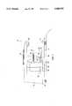
- FIG. 1is a schematic diagram of an atomic force microscope according to the present invention.
- FIG. 2is an isometric view of the atomic force microscope of FIG. 1.
- FIG. 3is a front view of an S-shaped scanner according to the present invention showing the application of scanning voltages thereto.
- FIG. 4is a rear view of the S-shaped scanner of FIG. 3.
- FIG. 5is a schematic diagram of an S-shaped scanner according to the present invention.
- Microscope 10comprises a base member 11 having a plurality of leveling screws 12 depending therefrom and supporting a flat pedestal 13 thereupon.
- Pedestal 13has a U-shaped opening 14 defined in the middle thereof.
- Microscope 10further comprises a vertical support member 15 with which a horizontal support mount 16 is integrally formed to extend outwardly therefrom.
- a laser adjustment attachment 18, a PZT tube scanner 19, and the detector position adjustment attachment 20are mounted on support mount 16 as hereinafter described in detail.
- U-shaped opening 14provides space in which to position sample stage 21 in operative relationship to PZT tube scanner 19.
- Base member 11preferably functions as a motorized translation stage to enable the height and the tilt of pedestal 13 to be adjusted as needed.
- PZT tube scanner 19One end of the PZT tube scanner 19 is attached to the bottom surface 17 of support mount 16. The other end of PZT tube scanner 19 is connected with cantilever holder 22 and beam tracking lens 23. A cantilever probe 24 is secured to the free end 25 of cantilever holder 22.
- a laser module 26such as a diode laser element is attached to laser adjustment attachment 18 as shown in FIG. 2 which, as described, is attached to support mount 16.
- Support mount 16has an opening 27 defined therethrough to allow the shank of laser module 26 to extend downwardly therethrough towards the cantilever probe 24.
- Laser module 26, thus positioned,produces a coherent, collimated laser light beam directed downwardly through beam tracking lens 23 toward the upper surface of cantilever probe 24.
- Detector position adjustment attachment 20comprises position sensitive photodetector module 28 and is likewise attached to support mount 16 adjacent to laser module 26.
- a clearance opening(not shown) is defined through support mount 16 to enable the photodetector embodied in position sensitive photodetector module 28 to receive laser light reflected from cantilever probe 24.
- An L-shaped support member 32is attached to the lower surface 33 of PZT tube scanner 19 and extends outwardly and upwardly therefrom.
- Lens support arm 34is integrally formed with L-shaped member 32 and extends outwardly therefrom.
- Beam tracking lens 23is seated within lens seating opening 36 formed in lens support arm 34 and secured thereto.
- the vertical arm 37 of L-shaped member 32will be the same length as the focal length of beam tracking lens 23.
- Cantilever holder 22is formed preferably of flat steel and is attached to the bottom portion of L-shaped member 32 and extends outwardly therefrom.
- the distal end 38 of cantilever holder 22carries cantilever probe 24 which is positioned directly under beam tracking lens 23.
- Sample stage 21is separate from pedestal 13 and the assembly of microscope 10 which is positioned on the top of motorized translational stage or base 11.
- Sample stage 21normally will be formed of a block of stainless steel having a thickness sufficient to allow a sample 40, which is located on top of sample stage 21 to be engaged by cantilever probe 24 within the mechanical travel distance of base 11 in response to leveling screws 12 which are preferably motor driven.
- base 11has three levelling screws 12 extending from the bottom which, in a preferred practice of this invention are controlled, individually, by three motors, or three thumb screws (not shown). The amount of available extension of the screws 12 governs the distance between the cantilever probe 24 and surface of sample 40.
- microscope 10comprises a sample stage 21 supporting sample 40 and the cantilever probe 24.
- a collimated diode laser module 26is mounted so as to remain stationary with respect to microscope 10 during operation of microscope 10.
- the cantilever probe or tip 24is attached to PZT tube scanner 19 directly and in fixed relationship to beam tracking lens 23 as shown.
- a beam tracking lens 23is attached, as described above, to L-shaped member 32.
- Beam tracking lens 23can be a commercial grade bi-convex lens (diameter 10 mm) of focal length 25 mm.
- Cantilever holder 22, including beam tracking lens 23,is so designed to be as light as possible (less than 20 g) and mechanically rigid.
- the moving beam tracking lens(moving with the movement of the lower surface 33 of PZT tube scanner 19) acts as a guide to the stationary laser beam to follow the moving cantilever.
- Such tracking actionis achieved based upon the geometric optical principal, that all rays passing through the beam tracking lens 23 go to one focal point, regardless of the positions of incidence at the lens aperture as shown in FIG. 1. If the upper reflective surface of cantilever probe 24 moves slightly out of the initial optic axis, the beam tracking lens 23 moves out of the axis the same amount, leaving the laser beam arriving at the outer portions of the lens, where the curvature of the lens makes the beam bend toward the axis. The degree of the bend is such that the beam is still focused at the focal point, which is fixed at the reflective back surface of the cantilever, thus the automatic tracking action is achieved without any complicated active-control elements.
- the position sensitive photodetector module 28 mounted within detector position adjustment attachment 20produces electrical signals indicating the change of the position of the light beam which is reflected from the reflective back of the moving cantilever 29.
- the electrical signal from the position detectoris the measure of the amount of the force of atomic interaction between the probe tip 24 the surface of sample 40. This is the result of the force causing the probe tip 24 to be pushed or pulled higher or lower thus producing a bend in the cantilever 29.
- Such bendingmakes the laser light beam, focused by the moving beam tracking lens 23, change its angle of deflection, which causes the reflected light beam to emerge in the direction of position sensitive photodetector module 28 with force-varying angles.
- cantilever probe 24also causes the absolute position of the focus to move. However, due to the intrinsic optical property, within the practical limit, such position changes do not contribute significantly to the direction of the reflected laser light beam. Therefore, only the reflection angle of the beam, which is proportional to the magnitude of the force acting on the cantilever probe 24, is the cause of the change of the position of the bright spot (due to the reflected laser light beam) on the position sensitive photodetector module 28.
- Imagesare recorded from microscope 10 using existing art equipment such as the Model TAC 3.0 available from AT Corp. of Tempe, Ariz.
- the beam tracking lens 23focuses all of the parallel incident light rays from laser module 26 into a fixed focused position below the cantilever probe 24.
- PZT tube scanner 19, beam tracking lens 23, cantilever probe 24 and cantilever holder 22are moved so that the cantilever probe 24 is translated across the desired area of the surface of sample 40 which remains stationary on sample stage 21.
- the laser beam detection with the optical lever methodis performed by using beam tracking lens 23 to guide the laser beam automatically with the moving cantilever probe 24.
- the present inventionprovides three noteworthy advantages compared to the conventional optical lever scheme.
- the cantilever probeis attached directly to the PZT tube scanner by the cantilever holder.
- a beam tracking lensis attached to the moving probe holder and to the bottom of the PZT tube scanner.
- an S-shaped PZT tube scanneris provided.
- the simple lensfocuses all of the parallel incident rays into a fixed focus position.
- the lenseliminates most errors.
- the cantileverIn order to move the cantilever, it is attached at the end of the scanning piezoceramic tube, which is controlled by the high voltages applied to the electrodes located at the side walls of the tube.
- the PZTWhen the PZT is bent by these voltages, it is accompanied by a tilt of the bottom surface as described by Carr, R. G. "Finite element analysis of PZT tube scanner motion for scanning tunneling microscopy", Journal of Microscopy, 152, pp. 379-385, 1988. This results in a large change in the probe height during scanning. The tilt is removed to less than experimental tolerances by using the special S-shaped scanner of this invention.
- this design and methodyields excellent images in AFM. See Jung and Yaniv, Electronics Letters, 29, No. 3, pp. 264-265.
- one of the electrodesis controlled by a scanning voltage, say, in the X direction (Vx+), and the opposite electrode is controlled by another voltage (Vx-) in the X direction.
- the tubebends by an amount proportional to the difference in the two high voltages in the X direction.
- each of the two electrodes facing each otherhas another controlling voltage in the Y direction in a similar fashion.
- Oneis Vy+ and the other is Vy-. Therefore, the tube will bend in the Y direction in response to the difference between Vy+ and Vy-.
- the inner surface of the tubesis covered with a separate cylindrical metallic electrode.
- a separate voltage to control the amount of the extension of the tubeis applied to that electrode (Vz).
- the amount of the voltage difference between the Vz and the average values of the Vx+, Vx-, Vy+ and Vy-determines the amount of the extension, which is used to adjust the height.
- the S-shaped scanner 19 as shown in FIGS. 3, 4 and 5is composed of two identical PZT scanners implemented one on the top of the other. Both parts have four independent electrodes around the side walls of the tube, thus the total number of independent electrodes in the S-shaped scanner of the current invention is eight. Each electrode occupies one quadrant and tracks on the side wall outer surface as shown in FIGS. 3 and 4 where "A" represents applied voltage Vx+, "B” represents Vx- voltage, "C” represents Vy- voltage, and "D” represents Vy+ applied voltage.
- the current inventiontwo of the tubes with the same electrode configuration as the prior art are used.
- the improvementis to make one body scanner by placing one on top of the other. This is achieved either by gluing two separately made PZT tubes together or separating the four quadrant electrodes by half, at the midway along the length of the scanner tube, thus realizing eight different electrodes. Then the top and bottom half electrodes are connected to the opposite polarities of the control voltages, such that if one of the top electrodes has Vx+, the bottom electrode at the same side has Vx- connected, and vice versa. At the orthogonal direction, Vy+is at the top, the Vy- is at the bottom, and vice versa. Therefore, although four additional electrodes are added, the number of necessary control voltages are the same, including the Vz which is connected at the inside electrode, to control the height as shown in FIG. 3.
- the tiltis created at the end of the section, which is the exact mid-point of the tube.
- the bottom partbends to the opposite direction, with exactly the same amount of the tilt but, in the opposite direction, because the relative polarities of the voltages are opposite. Therefore, the net tilt at the bottom of the overall tube is virtually eliminated, as long as the sections are of the identical property.
- the two sectionsbend to the opposite directions.
- the direction of the tilt of the top partis to the same direction of the bend, which makes the bottom part displaced to the same direction as the bending.
- the bottom partis bending toward the opposite direction.
- the top surface of the tubeis a fixed flat surface, and the bottom part bends from the tilt angle caused by the top section of the PZT tube toward the direction of the displacement.
- the bending of the bottom partalways leaves the overall net displacement to the direction of the bending of the top part. This result is obtained because the direction of the tilt is the same as the direction of the bending; the amount of the tilt is proportional to the amount of the bending; and the two sections are exactly identical to each other.
- FIG. 5shows the S-shaped bending of the present invention.
- the displacementis reduced by 1/2, which is compensated for by increasing the length of the PZT tube by 1.4 times.
Landscapes
- Physics & Mathematics (AREA)
- Health & Medical Sciences (AREA)
- General Health & Medical Sciences (AREA)
- General Physics & Mathematics (AREA)
- Nuclear Medicine, Radiotherapy & Molecular Imaging (AREA)
- Radiology & Medical Imaging (AREA)
- Length Measuring Devices With Unspecified Measuring Means (AREA)
Abstract
Description
R.sub.0 =(w.sup.2 +D.sup.2).sup.1/2
d.sub.L =1/2(L/R).sup.2
d.sub.s =2* 1/2×(L/R).sup.2 =1/4(L/R).sup.2
Claims (15)
Priority Applications (3)
| Application Number | Priority Date | Filing Date | Title |
|---|---|---|---|
| US08/190,948US5440920A (en) | 1994-02-03 | 1994-02-03 | Scanning force microscope with beam tracking lens |
| US08/427,353US5587523A (en) | 1994-02-03 | 1995-02-15 | Atomic force microscope employing beam tracking |
| US08/717,767US5763767A (en) | 1994-02-03 | 1996-09-23 | Atomic force microscope employing beam-tracking |
Applications Claiming Priority (1)
| Application Number | Priority Date | Filing Date | Title |
|---|---|---|---|
| US08/190,948US5440920A (en) | 1994-02-03 | 1994-02-03 | Scanning force microscope with beam tracking lens |
Related Child Applications (1)
| Application Number | Title | Priority Date | Filing Date |
|---|---|---|---|
| US08/427,353ContinuationUS5587523A (en) | 1994-02-03 | 1995-02-15 | Atomic force microscope employing beam tracking |
Publications (1)
| Publication Number | Publication Date |
|---|---|
| US5440920Atrue US5440920A (en) | 1995-08-15 |
Family
ID=22703454
Family Applications (3)
| Application Number | Title | Priority Date | Filing Date |
|---|---|---|---|
| US08/190,948Expired - LifetimeUS5440920A (en) | 1994-02-03 | 1994-02-03 | Scanning force microscope with beam tracking lens |
| US08/427,353Expired - LifetimeUS5587523A (en) | 1994-02-03 | 1995-02-15 | Atomic force microscope employing beam tracking |
| US08/717,767Expired - LifetimeUS5763767A (en) | 1994-02-03 | 1996-09-23 | Atomic force microscope employing beam-tracking |
Family Applications After (2)
| Application Number | Title | Priority Date | Filing Date |
|---|---|---|---|
| US08/427,353Expired - LifetimeUS5587523A (en) | 1994-02-03 | 1995-02-15 | Atomic force microscope employing beam tracking |
| US08/717,767Expired - LifetimeUS5763767A (en) | 1994-02-03 | 1996-09-23 | Atomic force microscope employing beam-tracking |
Country Status (1)
| Country | Link |
|---|---|
| US (3) | US5440920A (en) |
Cited By (29)
| Publication number | Priority date | Publication date | Assignee | Title |
|---|---|---|---|---|
| US5560244A (en)* | 1993-08-17 | 1996-10-01 | Digital Instruments, Inc. | Scanning stylus atomic force microscope with cantilever tracking and optical access |
| US5675154A (en)* | 1995-02-10 | 1997-10-07 | Molecular Imaging Corporation | Scanning probe microscope |
| US5811802A (en)* | 1995-08-18 | 1998-09-22 | Gamble; Ronald C. | Scanning probe microscope with hollow pivot assembly |
| US5861550A (en)* | 1997-10-14 | 1999-01-19 | Raymax Technology, Incorporated | Scanning force microscope |
| US5874669A (en)* | 1997-10-16 | 1999-02-23 | Raymax Technology, Inc. | Scanning force microscope with removable probe illuminator assembly |
| US5949070A (en)* | 1995-08-18 | 1999-09-07 | Gamble; Ronald C. | Scanning force microscope with integral laser-scanner-cantilever and independent stationary detector |
| US6018991A (en)* | 1994-08-11 | 2000-02-01 | Nikon Corporation | Scanning probe microscope having cantilever attached to driving member |
| US6032518A (en)* | 1993-08-17 | 2000-03-07 | Digital Instruments, Inc. | Scanning stylus atomic force microscope with cantilever tracking and optical access |
| WO2000019166A1 (en)* | 1998-09-26 | 2000-04-06 | Xidex Corporation | Multidimensional sensing system for atomic force miscroscopy |
| US6096559A (en)* | 1998-03-16 | 2000-08-01 | Lockheed Martin Energy Research Corporation | Micromechanical calorimetric sensor |
| US6138503A (en)* | 1997-10-16 | 2000-10-31 | Raymax Technology, Inc. | Scanning probe microscope system including removable probe sensor assembly |
| WO2002073125A1 (en)* | 2001-03-09 | 2002-09-19 | Veeco Instruments, Inc. | Apparatus and method for isolating and measuring movement in a metrology apparatus |
| US6455838B2 (en) | 1998-10-06 | 2002-09-24 | The Regents Of The University Of California | High sensitivity deflection sensing device |
| US6490913B1 (en) | 1995-05-19 | 2002-12-10 | The United States Of America As Represented By The Secretary Of Commerce | Humidity chamber for scanning stylus atomic force microscope with cantilever tracking |
| US20030185444A1 (en)* | 2002-01-10 | 2003-10-02 | Tadashi Honda | Handwriting information processing apparatus, handwriting information processing method, and storage medium having program stored therein for handwriting information processing |
| US20030233870A1 (en)* | 2001-07-18 | 2003-12-25 | Xidex Corporation | Multidimensional sensing system for atomic force microscopy |
| US6748795B1 (en) | 2001-07-27 | 2004-06-15 | Molecular Imaging Corporation | Pendulum scanner for scanning probe microscope |
| US20040216518A1 (en)* | 2001-08-27 | 2004-11-04 | Aaron Lewis | Multiple plate tip or sample scanning reconfigurable scanned probe microscope with transparent interfacing of far-field optical microscopes |
| US20060272398A1 (en)* | 2005-06-06 | 2006-12-07 | Academia Sinica | Beam tracking system for scanning-probe type atomic force microscope |
| KR100663196B1 (en) | 2006-03-28 | 2007-01-05 | (주) 랩시스템 | Integral probe mount and microscope comprising the same |
| US20070158554A1 (en)* | 2003-08-11 | 2007-07-12 | Japan Science And Technology Agency | Probe for probe microscope using transparent substrate, method of producing the same, and probe microscope device |
| US20080073519A1 (en)* | 2006-06-02 | 2008-03-27 | Psia Co, Ltd | Scanning probe microscope for measuring angle and method of measuring a sample using the same |
| US20080257022A1 (en)* | 2007-04-23 | 2008-10-23 | Frederick Sachs | Factory-alignable compact cantilever probe |
| US7767961B2 (en) | 2005-06-09 | 2010-08-03 | Hitachi Global Storage Technologies Netherlands B.V. | Method for determining material interfacial and metrology information of a sample using atomic force microscopy |
| US20110277192A1 (en)* | 2010-05-04 | 2011-11-10 | Park Sang-Il | Scanning probe microscope with drift compensation |
| CN102778588A (en)* | 2012-07-16 | 2012-11-14 | 北京航空航天大学 | Laser detecting device for high-speed atomic force microscope and detecting method thereof |
| US9097737B2 (en) | 2013-11-25 | 2015-08-04 | Oxford Instruments Asylum Research, Inc. | Modular atomic force microscope with environmental controls |
| CN105891548A (en)* | 2016-04-12 | 2016-08-24 | 中国人民解放军国防科学技术大学 | Nanoscale optical subsurface damage detection method based on ion sputtering technology |
| CN108020596A (en)* | 2016-11-04 | 2018-05-11 | Sonix公司 | Adjustable clamp for scanning acoustic microscope |
Families Citing this family (8)
| Publication number | Priority date | Publication date | Assignee | Title |
|---|---|---|---|---|
| SE0000555D0 (en)* | 2000-02-22 | 2000-02-22 | Nanofactory Instruments Ab | Measuring device for transmission electron microscope |
| SE0103781D0 (en)* | 2001-11-12 | 2001-11-12 | Nanofactory Instruments Ab | Electron microscope measuring device |
| JP4810251B2 (en)* | 2006-02-16 | 2011-11-09 | キヤノン株式会社 | Atomic force microscope |
| US7423264B2 (en)* | 2006-09-08 | 2008-09-09 | Kla-Tencor Technologies Corporation | Atomic force microscope |
| DE102006043352A1 (en)* | 2006-09-15 | 2008-03-27 | Westfälische Wilhelms-Universität Münster | Device for scanning a sample surface covered by a liquid |
| US7770231B2 (en) | 2007-08-02 | 2010-08-03 | Veeco Instruments, Inc. | Fast-scanning SPM and method of operating same |
| KR101590339B1 (en) | 2007-08-21 | 2016-02-01 | 에이일이삼 시스템즈 인코포레이티드 | Separator for electrochemical cell and method for its manufacture |
| JP2009128139A (en)* | 2007-11-22 | 2009-06-11 | Hitachi Ltd | Scanning probe microscope and probe unit for scanning probe microscope |
Citations (112)
| Publication number | Priority date | Publication date | Assignee | Title |
|---|---|---|---|---|
| US33387A (en)* | 1861-10-01 | Improvement in printing-presses | ||
| US34331A (en)* | 1862-02-04 | Improved blast-generator | ||
| US34489A (en)* | 1862-02-25 | Improvement in metallic cases for pictures, cards | ||
| US4343993A (en)* | 1979-09-20 | 1982-08-10 | International Business Machines Corporation | Scanning tunneling microscope |
| US4422002A (en)* | 1981-08-10 | 1983-12-20 | International Business Machines Corporation | Piezo-electric travelling support |
| US4520570A (en)* | 1983-12-30 | 1985-06-04 | International Business Machines Corporation | Piezoelectric x-y-positioner |
| US4668865A (en)* | 1985-03-07 | 1987-05-26 | International Business Machines Corporation | Scanning tunneling microscope |
| US4700075A (en)* | 1985-01-12 | 1987-10-13 | Carl-Zeiss-Stiftung | Detector for back-scattered electrons |
| US4724318A (en)* | 1985-11-26 | 1988-02-09 | International Business Machines Corporation | Atomic force microscope and method for imaging surfaces with atomic resolution |
| US4785177A (en)* | 1986-03-27 | 1988-11-15 | Kernforschungsanlage Julich Gesellschaft Mit Beschrankter Haftung | Kinematic arrangement for the micro-movements of objects |
| US4800274A (en)* | 1987-02-02 | 1989-01-24 | The Regents Of The University Of California | High resolution atomic force microscope |
| US4806755A (en)* | 1986-10-03 | 1989-02-21 | International Business Machines Corporation | Micromechanical atomic force sensor head |
| US4823004A (en)* | 1987-11-24 | 1989-04-18 | California Institute Of Technology | Tunnel and field effect carrier ballistics |
| US4837435A (en)* | 1987-06-25 | 1989-06-06 | Seiko Instruments Inc. | Tunneling scanning microscope having light source |
| US4866271A (en)* | 1986-07-11 | 1989-09-12 | Agency Of Industrial Science And Technology | Relative displacement control apparatus |
| US4868396A (en)* | 1987-10-13 | 1989-09-19 | Arizona Board Of Regents, Arizona State University | Cell and substrate for electrochemical STM studies |
| US4871938A (en)* | 1988-06-13 | 1989-10-03 | Digital Instruments, Inc. | Positioning device for a scanning tunneling microscope |
| US4877957A (en)* | 1986-07-14 | 1989-10-31 | Olympus Optical Co., Ltd. | Scanning type tunnel microscope |
| US4889988A (en)* | 1988-07-06 | 1989-12-26 | Digital Instruments, Inc. | Feedback control for scanning tunnel microscopes |
| US4902892A (en)* | 1987-10-15 | 1990-02-20 | Agency Of Industrial Science And Technology, Kosaka Laboratory Ltd. | Method of measurement by scanning tunneling microscope |
| US4914293A (en)* | 1988-03-04 | 1990-04-03 | Kabushiki Kaisha Toshiba | Microscope apparatus |
| US4924091A (en)* | 1989-02-01 | 1990-05-08 | The Regents Of The University Of California | Scanning ion conductance microscope |
| US4924104A (en)* | 1985-09-11 | 1990-05-08 | Ims Ionen Mikrofabrikations Systeme Gesellschaft M.B.H | Ion beam apparatus and method of modifying substrate |
| US4935634A (en)* | 1989-03-13 | 1990-06-19 | The Regents Of The University Of California | Atomic force microscope with optional replaceable fluid cell |
| US4947042A (en)* | 1988-12-13 | 1990-08-07 | Mitsubishi Denki Kabushiki Kaisha | Tunnel unit and scanning head for scanning tunneling microscope |
| US4952857A (en)* | 1989-03-24 | 1990-08-28 | Quanscan, Inc. | Scanning micromechanical probe control system |
| US4954704A (en)* | 1989-12-04 | 1990-09-04 | Digital Instruments, Inc. | Method to increase the speed of a scanning probe microscope |
| US4956817A (en)* | 1988-05-26 | 1990-09-11 | Quanscan, Inc. | High density data storage and retrieval system |
| US4962480A (en)* | 1987-09-10 | 1990-10-09 | Seiko Instruments, Inc. | Memory reading apparatus |
| USRE33387E (en) | 1985-11-26 | 1990-10-16 | International Business Machines Corporation | Atomic force microscope and method for imaging surfaces with atomic resolution |
| US4968914A (en)* | 1989-03-24 | 1990-11-06 | Quanscan, Inc. | High resolution electromechanical translation device |
| US4969978A (en)* | 1987-11-27 | 1990-11-13 | Seiko Instruments Inc. | Apparatus and method for tunnel current measurement observed simultaneously with electrochemical measurement |
| US4992728A (en)* | 1989-12-21 | 1991-02-12 | International Business Machines Corporation | Electrical probe incorporating scanning proximity microscope |
| US4992659A (en)* | 1989-07-27 | 1991-02-12 | International Business Machines Corporation | Near-field lorentz force microscopy |
| US4999494A (en)* | 1989-09-11 | 1991-03-12 | Digital Instruments, Inc. | System for scanning large sample areas with a scanning probe microscope |
| US4999495A (en)* | 1988-08-31 | 1991-03-12 | Seiko Instruments Inc. | Scanning tunneling microscope |
| US5003815A (en)* | 1989-10-20 | 1991-04-02 | International Business Machines Corporation | Atomic photo-absorption force microscope |
| US5009111A (en)* | 1988-08-31 | 1991-04-23 | Quanscan, Inc. | Differential force balance apparatus |
| US5013913A (en)* | 1988-07-23 | 1991-05-07 | Carl-Zeiss-Stiftung | Method of illuminating an object in a transmission electron microscope |
| US5017010A (en)* | 1989-05-16 | 1991-05-21 | International Business Machines Corporation | High sensitivity position sensor and method |
| US5018865A (en)* | 1988-10-21 | 1991-05-28 | Ferrell Thomas L | Photon scanning tunneling microscopy |
| US5022743A (en)* | 1987-03-27 | 1991-06-11 | The Board Of Trustees Of The Leland Stanford Junior University | Scanning confocal optical microscope |
| US5025658A (en)* | 1989-11-28 | 1991-06-25 | Digital Instruments, Inc. | Compact atomic force microscope |
| US5034903A (en)* | 1989-01-30 | 1991-07-23 | Alfano Robert R | Apparatus and method for measuring the time evolution of carriers propogating within submicron and micron electronic devices |
| US5047633A (en)* | 1989-05-08 | 1991-09-10 | Amersham International Plc | Imaging apparatus and method |
| US5051646A (en)* | 1989-04-28 | 1991-09-24 | Digital Instruments, Inc. | Method of driving a piezoelectric scanner linearly with time |
| US5066858A (en)* | 1990-04-18 | 1991-11-19 | Digital Instruments, Inc. | Scanning tunneling microscopes with correction for coupling effects |
| US5067805A (en)* | 1990-02-27 | 1991-11-26 | Prometrix Corporation | Confocal scanning optical microscope |
| US5077473A (en)* | 1990-07-26 | 1991-12-31 | Digital Instruments, Inc. | Drift compensation for scanning probe microscopes using an enhanced probe positioning system |
| US5081390A (en)* | 1990-08-13 | 1992-01-14 | Digital Instruments, Inc. | Method of operating a scanning probe microscope to improve drift characteristics |
| US5103095A (en)* | 1990-05-23 | 1992-04-07 | Digital Instruments, Inc. | Scanning probe microscope employing adjustable tilt and unitary head |
| US5107114A (en)* | 1990-09-14 | 1992-04-21 | Mitsubish Denki Kabushiki Kaisha | Fine scanning mechanism for atomic force microscope |
| US5107113A (en)* | 1990-12-26 | 1992-04-21 | Bell Communications Research, Inc. | Method and apparatus for correcting distortions in scanning tunneling microscope images |
| US5117110A (en)* | 1989-07-05 | 1992-05-26 | Seiko Instruments, Inc. | Composite scanning tunnelling microscope with a positioning function |
| US5120959A (en)* | 1989-01-31 | 1992-06-09 | Seiko Instruments Inc. | Apparatus for simultaneously effecting electrochemical measurement and measurement of tunneling current and tunnel probe therefor |
| US5142145A (en)* | 1989-07-05 | 1992-08-25 | Seiko Instruments, Inc. | Composite scanning tunneling microscope |
| US5141319A (en)* | 1990-11-22 | 1992-08-25 | Olympus Optical Co., Ltd. | Displacement detection device with adjacent semiconductor diode lasers |
| US5144833A (en)* | 1990-09-27 | 1992-09-08 | International Business Machines Corporation | Atomic force microscopy |
| US5155715A (en)* | 1989-01-13 | 1992-10-13 | Sharp Kabushiki Kaisha | Reproducing apparatus |
| US5155361A (en)* | 1991-07-26 | 1992-10-13 | The Arizona Board Of Regents, A Body Corporate Acting For And On Behalf Of Arizona State University | Potentiostatic preparation of molecular adsorbates for scanning probe microscopy |
| US5157251A (en)* | 1991-03-13 | 1992-10-20 | Park Scientific Instruments | Scanning force microscope having aligning and adjusting means |
| US5166516A (en)* | 1990-10-26 | 1992-11-24 | Olympus Optical Co., Ltd. | Scanning probe microscope with slant detection and compensation |
| US5168159A (en)* | 1990-11-19 | 1992-12-01 | Olympus Optical Co., Ltd. | Barrier height measuring apparatus including a conductive cantilever functioning as a tunnelling probe |
| US5189906A (en)* | 1989-11-28 | 1993-03-02 | Digital Instruments, Inc. | Compact atomic force microscope |
| US5196713A (en)* | 1991-08-22 | 1993-03-23 | Wyko Corporation | Optical position sensor with corner-cube and servo-feedback for scanning microscopes |
| US5198715A (en)* | 1990-05-23 | 1993-03-30 | Digital Instruments, Inc. | Scanner for scanning probe microscopes having reduced Z-axis non-linearity |
| US5202004A (en)* | 1989-12-20 | 1993-04-13 | Digital Instruments, Inc. | Scanning electrochemical microscopy |
| US5204531A (en)* | 1992-02-14 | 1993-04-20 | Digital Instruments, Inc. | Method of adjusting the size of the area scanned by a scanning probe |
| US5206702A (en)* | 1989-10-09 | 1993-04-27 | Olympus Optical Co., Ltd. | Technique for canceling the effect of external vibration on an atomic force microscope |
| US5210410A (en)* | 1991-09-26 | 1993-05-11 | The Board Of Trustees Of The Leland Stanford Junior University | Scanning probe microscope having scan correction |
| US5224376A (en)* | 1989-12-08 | 1993-07-06 | Digital Instruments, Inc. | Atomic force microscope |
| US5229606A (en)* | 1989-06-05 | 1993-07-20 | Digital Instruments, Inc. | Jumping probe microscope |
| US5231286A (en)* | 1990-08-31 | 1993-07-27 | Olympus Optical Co., Ltd. | Scanning probe microscope utilizing an optical element in a waveguide for dividing the center part of the laser beam perpendicular to the waveguide |
| USRE34331E (en) | 1988-07-06 | 1993-08-03 | Digital Instruments, Inc. | Feedback control for scanning tunnel microscopes |
| US5237859A (en)* | 1989-12-08 | 1993-08-24 | Digital Instruments, Inc. | Atomic force microscope |
| US5247186A (en)* | 1991-05-14 | 1993-09-21 | Olympus Optical Co., Ltd. | Integrated optical displacement sensor |
| US5245863A (en)* | 1990-07-11 | 1993-09-21 | Olympus Optical Co., Ltd. | Atomic probe microscope |
| US5253516A (en)* | 1990-05-23 | 1993-10-19 | Digital Instruments, Inc. | Atomic force microscope for small samples having dual-mode operating capability |
| US5257024A (en)* | 1988-05-26 | 1993-10-26 | Quan-Scan, Inc. | Search position encoder |
| US5258107A (en)* | 1991-05-28 | 1993-11-02 | Seiko Instruments Inc. | Method for manufacturing a cantilever with sharpened metal needle |
| US5260824A (en)* | 1989-04-24 | 1993-11-09 | Olympus Optical Co., Ltd. | Atomic force microscope |
| US5260567A (en)* | 1991-04-10 | 1993-11-09 | Canon Kabushiki Kaisha | Cantilever unit and atomic force microscope, magnetic force microscope, reproducing apparatus and information processing apparatus using the cantilever unit |
| US5260622A (en)* | 1989-03-24 | 1993-11-09 | Topometrix Corporation | High resolution electromechanical translation device |
| US5262643A (en)* | 1992-06-12 | 1993-11-16 | International Business Machines Corp. | Automatic tip approach method and apparatus for scanning probe microscope |
| US5266801A (en)* | 1989-06-05 | 1993-11-30 | Digital Instruments, Inc. | Jumping probe microscope |
| US5266897A (en)* | 1990-09-05 | 1993-11-30 | International Business Machines Corporation | Magnetic field observation with tunneling microscopy |
| US5266896A (en)* | 1992-06-09 | 1993-11-30 | International Business Machines Corporation | Mechanical detection and imaging of magnetic resonance by magnetic moment modulation |
| US5267471A (en)* | 1992-04-30 | 1993-12-07 | Ibm Corporation | Double cantilever sensor for atomic force microscope |
| US5274230A (en)* | 1990-08-31 | 1993-12-28 | Olympus Optical Co., Ltd. | Scanning probe microscope having first and second optical waveguides |
| US5276324A (en)* | 1991-08-08 | 1994-01-04 | Nikon Corporation | Composite scanning tunneling microscope |
| US5280341A (en)* | 1992-02-27 | 1994-01-18 | International Business Machines Corporation | Feedback controlled differential fiber interferometer |
| US5283437A (en)* | 1990-12-21 | 1994-02-01 | International Business Machines Corporation | Pneumatically and electrostatically driven scanning tunneling microscope |
| US5283442A (en)* | 1992-02-04 | 1994-02-01 | International Business Machines Corporation | Surface profiling using scanning force microscopy |
| US5286977A (en)* | 1992-01-23 | 1994-02-15 | Matsushita Electric Industrial Co., Ltd. | Positioning device |
| US5289004A (en)* | 1990-03-27 | 1994-02-22 | Olympus Optical Co., Ltd. | Scanning probe microscope having cantilever and detecting sample characteristics by means of reflected sample examination light |
| US5291775A (en)* | 1992-03-04 | 1994-03-08 | Topometrix | Scanning force microscope with integrated optics and cantilever mount |
| US5293042A (en)* | 1991-05-10 | 1994-03-08 | Olympus Optical Co., Ltd. | Servo circuit of scanning probe microscope |
| US5294804A (en)* | 1992-03-11 | 1994-03-15 | Olympus Optical Co., Ltd. | Cantilever displacement detection apparatus |
| US5296704A (en)* | 1989-10-02 | 1994-03-22 | Olympus Optical Co., Ltd. | Scanning tunneling microscope |
| US5298975A (en)* | 1991-09-27 | 1994-03-29 | International Business Machines Corporation | Combined scanning force microscope and optical metrology tool |
| US5304924A (en)* | 1989-03-29 | 1994-04-19 | Canon Kabushiki Kaisha | Edge detector |
| US5306919A (en)* | 1992-09-21 | 1994-04-26 | Digital Instruments, Inc. | Positioning device for scanning probe microscopes |
| US5308974A (en) | 1992-11-30 | 1994-05-03 | Digital Instruments, Inc. | Scanning probe microscope using stored data for vertical probe positioning |
| US5307693A (en) | 1993-01-21 | 1994-05-03 | At&T Bell Laboratories | Force-sensing system, including a magnetically mounted rocking element |
| US5314254A (en) | 1992-11-03 | 1994-05-24 | Digital Instruments | Stiffness enhancer for movable stage assembly |
| US5314829A (en) | 1992-12-18 | 1994-05-24 | California Institute Of Technology | Method for imaging informational biological molecules on a semiconductor substrate |
| US5317153A (en) | 1991-08-08 | 1994-05-31 | Nikon Corporation | Scanning probe microscope |
| US5319960A (en) | 1992-03-06 | 1994-06-14 | Topometrix | Scanning force microscope |
| US5323003A (en) | 1991-09-03 | 1994-06-21 | Canon Kabushiki Kaisha | Scanning probe microscope and method of observing sample by using such a microscope |
| US5321977A (en) | 1992-12-31 | 1994-06-21 | International Business Machines Corporation | Integrated tip strain sensor for use in combination with a single axis atomic force microscope |
| US5324935A (en) | 1992-05-08 | 1994-06-28 | Seiko Instruments Inc. | Scanning probe microscope having a directional coupler and a Z-direction distance adjusting piezoelectric element |
| US5325010A (en) | 1988-07-03 | 1994-06-28 | Forschungszentrum Julich Gmbh | Micromanipulator |
Family Cites Families (9)
| Publication number | Priority date | Publication date | Assignee | Title |
|---|---|---|---|---|
| US4968390A (en)* | 1988-11-03 | 1990-11-06 | Board Of Regents, The University Of Texas System | High resolution deposition and etching in polymer films |
| JPH02311702A (en)* | 1989-05-29 | 1990-12-27 | Olympus Optical Co Ltd | Scanning type tunnel microscope apparatus |
| GB2235571B (en)* | 1989-06-26 | 1993-11-17 | Jeol Ltd | Scanning tunnelling microscope |
| JPH0756443B2 (en)* | 1990-12-20 | 1995-06-14 | 株式会社島津製作所 | Scanning tunnel microscope for observing biological samples |
| US5408094A (en) | 1992-05-07 | 1995-04-18 | Olympus Optical Co., Ltd. | Atomic force microscope with light beam emission at predetermined angle |
| JP3000500B2 (en) | 1992-09-02 | 2000-01-17 | セイコーインスツルメンツ株式会社 | Atomic force microscope |
| US5406832A (en) | 1993-07-02 | 1995-04-18 | Topometrix Corporation | Synchronous sampling scanning force microscope |
| US5388452A (en) | 1993-10-15 | 1995-02-14 | Quesant Instrument Corporation | Detection system for atomic force microscopes |
| US5357105A (en) | 1993-11-09 | 1994-10-18 | Quesant Instrument Corporation | Light modulated detection system for atomic force microscopes |
- 1994
- 1994-02-03USUS08/190,948patent/US5440920A/ennot_activeExpired - Lifetime
- 1995
- 1995-02-15USUS08/427,353patent/US5587523A/ennot_activeExpired - Lifetime
- 1996
- 1996-09-23USUS08/717,767patent/US5763767A/ennot_activeExpired - Lifetime
Patent Citations (115)
| Publication number | Priority date | Publication date | Assignee | Title |
|---|---|---|---|---|
| US34331A (en)* | 1862-02-04 | Improved blast-generator | ||
| US34489A (en)* | 1862-02-25 | Improvement in metallic cases for pictures, cards | ||
| US33387A (en)* | 1861-10-01 | Improvement in printing-presses | ||
| US4343993A (en)* | 1979-09-20 | 1982-08-10 | International Business Machines Corporation | Scanning tunneling microscope |
| US4422002A (en)* | 1981-08-10 | 1983-12-20 | International Business Machines Corporation | Piezo-electric travelling support |
| US4520570A (en)* | 1983-12-30 | 1985-06-04 | International Business Machines Corporation | Piezoelectric x-y-positioner |
| US4700075A (en)* | 1985-01-12 | 1987-10-13 | Carl-Zeiss-Stiftung | Detector for back-scattered electrons |
| US4668865A (en)* | 1985-03-07 | 1987-05-26 | International Business Machines Corporation | Scanning tunneling microscope |
| US4924104A (en)* | 1985-09-11 | 1990-05-08 | Ims Ionen Mikrofabrikations Systeme Gesellschaft M.B.H | Ion beam apparatus and method of modifying substrate |
| US4724318A (en)* | 1985-11-26 | 1988-02-09 | International Business Machines Corporation | Atomic force microscope and method for imaging surfaces with atomic resolution |
| USRE33387E (en) | 1985-11-26 | 1990-10-16 | International Business Machines Corporation | Atomic force microscope and method for imaging surfaces with atomic resolution |
| US4785177A (en)* | 1986-03-27 | 1988-11-15 | Kernforschungsanlage Julich Gesellschaft Mit Beschrankter Haftung | Kinematic arrangement for the micro-movements of objects |
| US4866271A (en)* | 1986-07-11 | 1989-09-12 | Agency Of Industrial Science And Technology | Relative displacement control apparatus |
| US4877957A (en)* | 1986-07-14 | 1989-10-31 | Olympus Optical Co., Ltd. | Scanning type tunnel microscope |
| US4806755A (en)* | 1986-10-03 | 1989-02-21 | International Business Machines Corporation | Micromechanical atomic force sensor head |
| US4800274A (en)* | 1987-02-02 | 1989-01-24 | The Regents Of The University Of California | High resolution atomic force microscope |
| US5022743A (en)* | 1987-03-27 | 1991-06-11 | The Board Of Trustees Of The Leland Stanford Junior University | Scanning confocal optical microscope |
| US4837435A (en)* | 1987-06-25 | 1989-06-06 | Seiko Instruments Inc. | Tunneling scanning microscope having light source |
| US4962480A (en)* | 1987-09-10 | 1990-10-09 | Seiko Instruments, Inc. | Memory reading apparatus |
| US4868396A (en)* | 1987-10-13 | 1989-09-19 | Arizona Board Of Regents, Arizona State University | Cell and substrate for electrochemical STM studies |
| US4902892A (en)* | 1987-10-15 | 1990-02-20 | Agency Of Industrial Science And Technology, Kosaka Laboratory Ltd. | Method of measurement by scanning tunneling microscope |
| US4823004A (en)* | 1987-11-24 | 1989-04-18 | California Institute Of Technology | Tunnel and field effect carrier ballistics |
| US4969978A (en)* | 1987-11-27 | 1990-11-13 | Seiko Instruments Inc. | Apparatus and method for tunnel current measurement observed simultaneously with electrochemical measurement |
| US4914293A (en)* | 1988-03-04 | 1990-04-03 | Kabushiki Kaisha Toshiba | Microscope apparatus |
| US5257024A (en)* | 1988-05-26 | 1993-10-26 | Quan-Scan, Inc. | Search position encoder |
| US4956817A (en)* | 1988-05-26 | 1990-09-11 | Quanscan, Inc. | High density data storage and retrieval system |
| US4871938A (en)* | 1988-06-13 | 1989-10-03 | Digital Instruments, Inc. | Positioning device for a scanning tunneling microscope |
| US5325010A (en) | 1988-07-03 | 1994-06-28 | Forschungszentrum Julich Gmbh | Micromanipulator |
| USRE34331E (en) | 1988-07-06 | 1993-08-03 | Digital Instruments, Inc. | Feedback control for scanning tunnel microscopes |
| US4889988A (en)* | 1988-07-06 | 1989-12-26 | Digital Instruments, Inc. | Feedback control for scanning tunnel microscopes |
| US5013913A (en)* | 1988-07-23 | 1991-05-07 | Carl-Zeiss-Stiftung | Method of illuminating an object in a transmission electron microscope |
| US5009111A (en)* | 1988-08-31 | 1991-04-23 | Quanscan, Inc. | Differential force balance apparatus |
| US4999495A (en)* | 1988-08-31 | 1991-03-12 | Seiko Instruments Inc. | Scanning tunneling microscope |
| US5018865A (en)* | 1988-10-21 | 1991-05-28 | Ferrell Thomas L | Photon scanning tunneling microscopy |
| US4947042A (en)* | 1988-12-13 | 1990-08-07 | Mitsubishi Denki Kabushiki Kaisha | Tunnel unit and scanning head for scanning tunneling microscope |
| US5155715A (en)* | 1989-01-13 | 1992-10-13 | Sharp Kabushiki Kaisha | Reproducing apparatus |
| US5034903A (en)* | 1989-01-30 | 1991-07-23 | Alfano Robert R | Apparatus and method for measuring the time evolution of carriers propogating within submicron and micron electronic devices |
| US5120959A (en)* | 1989-01-31 | 1992-06-09 | Seiko Instruments Inc. | Apparatus for simultaneously effecting electrochemical measurement and measurement of tunneling current and tunnel probe therefor |
| US4924091A (en)* | 1989-02-01 | 1990-05-08 | The Regents Of The University Of California | Scanning ion conductance microscope |
| USRE34489E (en) | 1989-03-13 | 1993-12-28 | The Regents Of The University Of California | Atomic force microscope with optional replaceable fluid cell |
| USRE34489F1 (en) | 1989-03-13 | 1999-12-14 | Univ California | Atomic force microscope with optimal replacement fluid cell |
| US4935634A (en)* | 1989-03-13 | 1990-06-19 | The Regents Of The University Of California | Atomic force microscope with optional replaceable fluid cell |
| US4968914A (en)* | 1989-03-24 | 1990-11-06 | Quanscan, Inc. | High resolution electromechanical translation device |
| US5260622A (en)* | 1989-03-24 | 1993-11-09 | Topometrix Corporation | High resolution electromechanical translation device |
| US4952857A (en)* | 1989-03-24 | 1990-08-28 | Quanscan, Inc. | Scanning micromechanical probe control system |
| US5304924A (en)* | 1989-03-29 | 1994-04-19 | Canon Kabushiki Kaisha | Edge detector |
| US5260824A (en)* | 1989-04-24 | 1993-11-09 | Olympus Optical Co., Ltd. | Atomic force microscope |
| US5051646A (en)* | 1989-04-28 | 1991-09-24 | Digital Instruments, Inc. | Method of driving a piezoelectric scanner linearly with time |
| US5047633A (en)* | 1989-05-08 | 1991-09-10 | Amersham International Plc | Imaging apparatus and method |
| US5017010A (en)* | 1989-05-16 | 1991-05-21 | International Business Machines Corporation | High sensitivity position sensor and method |
| US5266801A (en)* | 1989-06-05 | 1993-11-30 | Digital Instruments, Inc. | Jumping probe microscope |
| US5229606A (en)* | 1989-06-05 | 1993-07-20 | Digital Instruments, Inc. | Jumping probe microscope |
| US5142145A (en)* | 1989-07-05 | 1992-08-25 | Seiko Instruments, Inc. | Composite scanning tunneling microscope |
| US5117110A (en)* | 1989-07-05 | 1992-05-26 | Seiko Instruments, Inc. | Composite scanning tunnelling microscope with a positioning function |
| US4992659A (en)* | 1989-07-27 | 1991-02-12 | International Business Machines Corporation | Near-field lorentz force microscopy |
| US4999494A (en)* | 1989-09-11 | 1991-03-12 | Digital Instruments, Inc. | System for scanning large sample areas with a scanning probe microscope |
| US5296704A (en)* | 1989-10-02 | 1994-03-22 | Olympus Optical Co., Ltd. | Scanning tunneling microscope |
| US5206702A (en)* | 1989-10-09 | 1993-04-27 | Olympus Optical Co., Ltd. | Technique for canceling the effect of external vibration on an atomic force microscope |
| US5003815A (en)* | 1989-10-20 | 1991-04-02 | International Business Machines Corporation | Atomic photo-absorption force microscope |
| US5025658A (en)* | 1989-11-28 | 1991-06-25 | Digital Instruments, Inc. | Compact atomic force microscope |
| US5189906A (en)* | 1989-11-28 | 1993-03-02 | Digital Instruments, Inc. | Compact atomic force microscope |
| US4954704A (en)* | 1989-12-04 | 1990-09-04 | Digital Instruments, Inc. | Method to increase the speed of a scanning probe microscope |
| US5237859A (en)* | 1989-12-08 | 1993-08-24 | Digital Instruments, Inc. | Atomic force microscope |
| US5224376A (en)* | 1989-12-08 | 1993-07-06 | Digital Instruments, Inc. | Atomic force microscope |
| US5202004A (en)* | 1989-12-20 | 1993-04-13 | Digital Instruments, Inc. | Scanning electrochemical microscopy |
| US4992728A (en)* | 1989-12-21 | 1991-02-12 | International Business Machines Corporation | Electrical probe incorporating scanning proximity microscope |
| US5067805A (en)* | 1990-02-27 | 1991-11-26 | Prometrix Corporation | Confocal scanning optical microscope |
| US5289004A (en)* | 1990-03-27 | 1994-02-22 | Olympus Optical Co., Ltd. | Scanning probe microscope having cantilever and detecting sample characteristics by means of reflected sample examination light |
| US5066858A (en)* | 1990-04-18 | 1991-11-19 | Digital Instruments, Inc. | Scanning tunneling microscopes with correction for coupling effects |
| US5198715A (en)* | 1990-05-23 | 1993-03-30 | Digital Instruments, Inc. | Scanner for scanning probe microscopes having reduced Z-axis non-linearity |
| US5103095A (en)* | 1990-05-23 | 1992-04-07 | Digital Instruments, Inc. | Scanning probe microscope employing adjustable tilt and unitary head |
| US5253516A (en)* | 1990-05-23 | 1993-10-19 | Digital Instruments, Inc. | Atomic force microscope for small samples having dual-mode operating capability |
| US5245863A (en)* | 1990-07-11 | 1993-09-21 | Olympus Optical Co., Ltd. | Atomic probe microscope |
| US5077473A (en)* | 1990-07-26 | 1991-12-31 | Digital Instruments, Inc. | Drift compensation for scanning probe microscopes using an enhanced probe positioning system |
| US5081390A (en)* | 1990-08-13 | 1992-01-14 | Digital Instruments, Inc. | Method of operating a scanning probe microscope to improve drift characteristics |
| US5274230A (en)* | 1990-08-31 | 1993-12-28 | Olympus Optical Co., Ltd. | Scanning probe microscope having first and second optical waveguides |
| US5231286A (en)* | 1990-08-31 | 1993-07-27 | Olympus Optical Co., Ltd. | Scanning probe microscope utilizing an optical element in a waveguide for dividing the center part of the laser beam perpendicular to the waveguide |
| US5266897A (en)* | 1990-09-05 | 1993-11-30 | International Business Machines Corporation | Magnetic field observation with tunneling microscopy |
| US5107114A (en)* | 1990-09-14 | 1992-04-21 | Mitsubish Denki Kabushiki Kaisha | Fine scanning mechanism for atomic force microscope |
| US5144833A (en)* | 1990-09-27 | 1992-09-08 | International Business Machines Corporation | Atomic force microscopy |
| US5166516A (en)* | 1990-10-26 | 1992-11-24 | Olympus Optical Co., Ltd. | Scanning probe microscope with slant detection and compensation |
| US5168159A (en)* | 1990-11-19 | 1992-12-01 | Olympus Optical Co., Ltd. | Barrier height measuring apparatus including a conductive cantilever functioning as a tunnelling probe |
| US5141319A (en)* | 1990-11-22 | 1992-08-25 | Olympus Optical Co., Ltd. | Displacement detection device with adjacent semiconductor diode lasers |
| US5283437A (en)* | 1990-12-21 | 1994-02-01 | International Business Machines Corporation | Pneumatically and electrostatically driven scanning tunneling microscope |
| US5107113A (en)* | 1990-12-26 | 1992-04-21 | Bell Communications Research, Inc. | Method and apparatus for correcting distortions in scanning tunneling microscope images |
| US5157251A (en)* | 1991-03-13 | 1992-10-20 | Park Scientific Instruments | Scanning force microscope having aligning and adjusting means |
| US5260567A (en)* | 1991-04-10 | 1993-11-09 | Canon Kabushiki Kaisha | Cantilever unit and atomic force microscope, magnetic force microscope, reproducing apparatus and information processing apparatus using the cantilever unit |
| US5293042A (en)* | 1991-05-10 | 1994-03-08 | Olympus Optical Co., Ltd. | Servo circuit of scanning probe microscope |
| US5247186A (en)* | 1991-05-14 | 1993-09-21 | Olympus Optical Co., Ltd. | Integrated optical displacement sensor |
| US5258107A (en)* | 1991-05-28 | 1993-11-02 | Seiko Instruments Inc. | Method for manufacturing a cantilever with sharpened metal needle |
| US5155361A (en)* | 1991-07-26 | 1992-10-13 | The Arizona Board Of Regents, A Body Corporate Acting For And On Behalf Of Arizona State University | Potentiostatic preparation of molecular adsorbates for scanning probe microscopy |
| US5276324A (en)* | 1991-08-08 | 1994-01-04 | Nikon Corporation | Composite scanning tunneling microscope |
| US5317153A (en) | 1991-08-08 | 1994-05-31 | Nikon Corporation | Scanning probe microscope |
| US5196713A (en)* | 1991-08-22 | 1993-03-23 | Wyko Corporation | Optical position sensor with corner-cube and servo-feedback for scanning microscopes |
| US5323003A (en) | 1991-09-03 | 1994-06-21 | Canon Kabushiki Kaisha | Scanning probe microscope and method of observing sample by using such a microscope |
| US5210410A (en)* | 1991-09-26 | 1993-05-11 | The Board Of Trustees Of The Leland Stanford Junior University | Scanning probe microscope having scan correction |
| US5298975A (en)* | 1991-09-27 | 1994-03-29 | International Business Machines Corporation | Combined scanning force microscope and optical metrology tool |
| US5286977A (en)* | 1992-01-23 | 1994-02-15 | Matsushita Electric Industrial Co., Ltd. | Positioning device |
| US5283442A (en)* | 1992-02-04 | 1994-02-01 | International Business Machines Corporation | Surface profiling using scanning force microscopy |
| US5204531A (en)* | 1992-02-14 | 1993-04-20 | Digital Instruments, Inc. | Method of adjusting the size of the area scanned by a scanning probe |
| US5280341A (en)* | 1992-02-27 | 1994-01-18 | International Business Machines Corporation | Feedback controlled differential fiber interferometer |
| US5291775A (en)* | 1992-03-04 | 1994-03-08 | Topometrix | Scanning force microscope with integrated optics and cantilever mount |
| US5319960A (en) | 1992-03-06 | 1994-06-14 | Topometrix | Scanning force microscope |
| US5294804A (en)* | 1992-03-11 | 1994-03-15 | Olympus Optical Co., Ltd. | Cantilever displacement detection apparatus |
| US5267471A (en)* | 1992-04-30 | 1993-12-07 | Ibm Corporation | Double cantilever sensor for atomic force microscope |
| US5324935A (en) | 1992-05-08 | 1994-06-28 | Seiko Instruments Inc. | Scanning probe microscope having a directional coupler and a Z-direction distance adjusting piezoelectric element |
| US5266896A (en)* | 1992-06-09 | 1993-11-30 | International Business Machines Corporation | Mechanical detection and imaging of magnetic resonance by magnetic moment modulation |
| US5262643A (en)* | 1992-06-12 | 1993-11-16 | International Business Machines Corp. | Automatic tip approach method and apparatus for scanning probe microscope |
| US5306919A (en)* | 1992-09-21 | 1994-04-26 | Digital Instruments, Inc. | Positioning device for scanning probe microscopes |
| US5314254A (en) | 1992-11-03 | 1994-05-24 | Digital Instruments | Stiffness enhancer for movable stage assembly |
| US5308974A (en) | 1992-11-30 | 1994-05-03 | Digital Instruments, Inc. | Scanning probe microscope using stored data for vertical probe positioning |
| US5308974B1 (en) | 1992-11-30 | 1998-01-06 | Digital Instr Inc | Scanning probe microscope using stored data for vertical probe positioning |
| US5314829A (en) | 1992-12-18 | 1994-05-24 | California Institute Of Technology | Method for imaging informational biological molecules on a semiconductor substrate |
| US5321977A (en) | 1992-12-31 | 1994-06-21 | International Business Machines Corporation | Integrated tip strain sensor for use in combination with a single axis atomic force microscope |
| US5307693A (en) | 1993-01-21 | 1994-05-03 | At&T Bell Laboratories | Force-sensing system, including a magnetically mounted rocking element |
Non-Patent Citations (53)
| Title |
|---|
| Allan J. Melmed, "Art and Science and other Aspects of Making Sharp Tips", J. Vac. Sci. Technol. B 9(2), pp. 601-608, Mar./Apr. 1991. |
| Allan J. Melmed, Art and Science and other Aspects of Making Sharp Tips , J. Vac. Sci. Technol. B 9(2), pp. 601 608, Mar./Apr. 1991.* |
| B. B. Damaskin, "Comprehensive Treatise of Electrochemistry vol. 1: Chapter 8: The Absorption of Organic Molecules", pp. 353-395. |
| B. B. Damaskin, Comprehensive Treatise of Electrochemistry vol. 1: Chapter 8: The Absorption of Organic Molecules , pp. 353 395.* |
| B. Drake, "Imaging Crystals, Polymers, and Processes in Water with the Atomic Force Microscope", Science, vol. 243, pp. 1586-1589, Mar. 24, 1989. |
| B. Drake, Imaging Crystals, Polymers, and Processes in Water with the Atomic Force Microscope , Science, vol. 243, pp. 1586 1589, Mar. 24, 1989.* |
| C. Mathew Mate, "Research Report--Determination of Lubricant Film Thickness on A Particulate Disk Surface by Atomic Force Microscopy", Apr. 25, 1989. |
| C. Mathew Mate, "Research Report-Determination of Lubricant Film Thickness on A Particulate Disk Surface by Atomic Force Microscopy", Magnetic Recording RJ 6789 (64857), April. 25, 1989.* |
| Exhibit A, John Adam Kramer, Candidacy Report, pp. 1-48, May 21, 1985. |
| Exhibit B, Paul West, "Chemical Applications of Scanning Tunneling Microscopy", IBM J. Res. Develop. vol. 30(5), pp. 484-490, Sep. 1986. |
| Exhibit C, p. 691, Texas Instruments Inc. copyright 1986.* |
| F. Ohnesorge, "True Atomic Resolution by Atomic Force Microscopy Through Repulsive and Attractive Forces", Science vol. 260, pp. 1451-1456, Jun. 4, 1993. |
| F. Ohnesorge, True Atomic Resolution by Atomic Force Microscopy Through Repulsive and Attractive Forces , Science vol. 260, pp. 1451 1456, Jun. 4, 1993.* |
| G. Binnig, "Single-Tube Three-Dimensional Scanner for Scanning Tunneling Microscopy", Rev. Sci. Instrum. 57(8), pp. 1688-1689, Aug. 1986. |
| G. Binnig, Single Tube Three Dimensional Scanner for Scanning Tunneling Microscopy , Rev. Sci. Instrum. 57(8), pp. 1688 1689, Aug. 1986.* |
| G. Travaglini, "Scanning Tunneling Microscopy on Biological Matter", Surface Science 181, pp. 380-390, 1987. |
| G. Travaglini, Scanning Tunneling Microscopy on Biological Matter , Surface Science 181, pp. 380 390, 1987.* |
| H. Hanselmann, "Implementation of Digital Controllers-A Survey", Automatica, vol. 23(1) pp. 7-32, 1987. |
| H. Hanselmann, Implementation of Digital Controllers A Survey , Automatica, vol. 23(1) pp. 7 32, 1987.* |
| Inga Holl Musselman, "Platinum/Iridium Tips with Controlled Geometry for Scanning Tunneling Microscopy", J. Vac. Sci. Technol. A, vol. 8(4), pp. 3570-3575 Jul./Aug. 1990.* |
| Inga Holl Musselman, "Platinum/Iridium Tips with Controlled Geometry Tunneling Microscopy", J. Vac. Sci. Technol. A, vol. 8(4), pp. 3558-3562 Jul./Aug. 1990. |
| J. P. Ibe, "On the Electrochemical Etching of Tips for Scanning Tunneling Microscopy", J. Vac. Sci. Technol. A, vol. 8(4), pp. 3570-3575, Jul./Aug. 1990. |
| J. P. Ibe, On the Electrochemical Etching of Tips for Scanning Tunneling Microscopy , J. Vac. Sci. Technol. A, vol. 8(4), pp. 3570 3575, Jul./Aug. 1990.* |
| John Adam Kramer, Candidacy Report, pp. 1-48, May 21, 1985.* |
| Jung et al., "Novel Stationary-Sample Atomic Force Microscope with Beam-Tracking Lens", Electronic Letters, vol. 19, No. 3, 4 Feb. 1993, pp. 264-265.* |
| Jung et al., "Novel Stationary-Sample Atomic Force Microscope with Beam-Tracking Lens", Electronic Letters, vol. 29, No. 3, 14 Dec. 1992, pp. 264-265. |
| L. A. Nagahara, "Preparation and Characterization of STM Tips for Electrochemical Studies". |
| L.A. Nagahara, "Preparation and Characterization of STM Tips for Electrochemical Studies", Rev. Sci. Instrum. 60(10), pp. 3128-3130, October 1989.* |
| M. Brede, "Brittle Crack Propagation in Silicon Single Crystals", J. Appl. Phys. 70(2), pp. 758-771, Jul. 15, 1991. |
| M. Brede, Brittle Crack Propagation in Silicon Single Crystals , J. Appl. Phys. 70(2), pp. 758 771, Jul. 15, 1991.* |
| M. D. Kirk, "Low Temperature Atomic Force Microscopy", Rev. Sci. Instrum. 59(6), pp. 833-835, Jun. 1988. |
| M. D. Kirk, Low Temperature Atomic Force Microscopy , Rev. Sci. Instrum. 59(6), pp. 833 835, Jun. 1988.* |
| Martin Specht, "Simultaneous Measurement of Tunneling Current and Force as a Function of Position Through A Lipid Film on A Solid Substrate", Surface Science Letters 257, pp. L653-658, 1991. |
| Martin Specht, Simultaneous Measurement of Tunneling Current and Force as a Function of Position Through A Lipid Film on A Solid Substrate , Surface Science Letters 257, pp. L653 658, 1991.* |
| O. Marti, "Atomic Force Microscopy of Liquid-covered Surfaces: Atomic Resolution Images", Appl. Phys. Lett. 51(7), pp. 484-486, Aug. 17, 1987. |
| O. Marti, "Control Electronics for Atomic Force Microscopy", Rev. Sci. Instrum., vol. 59(6) pp. 836-839, Jun. 1988. |
| O. Marti, Atomic Force Microscopy of Liquid covered Surfaces: Atomic Resolution Images , Appl. Phys. Lett. 51(7), pp. 484 486, Aug. 17, 1987.* |
| O. Marti, Control Electronics for Atomic Force Microscopy , Rev. Sci. Instrum., vol. 59(6) pp. 836 839, Jun. 1988.* |
| P. Davidson, "A New Symmetric Scanning Tunneling Microscope Design", Journal of Vacuum Science & Technology: Part A, pp. 380-382, Mar./Apr. 1986. |
| P. Davidsson, "A New Symmetric Scanning Tunneling Microscope Design", Journal of Vacuum Science & Technology: Part A, pp. 380-382, Mar./Apr. 1988.* |
| Paul West, "Chemical Applications of Scanning Tunneling Microscopy", IBM J. Res. Develop. vol. 30(5), pp. 484-490, Sep. 1986.* |
| Richard Sonnenfeld, "Atomic-Resolution Microscopy in Water", Science, vol. 232, pp. 211-213, Apr. 11, 1986. |
| Richard Sonnenfeld, "Semiconductor Topography in Aqueous Environments: Tunneling Microscopy of Chemomechanically Polished (001) GaAs", 320 Applied Physics Letters 50(24), pp. 1742-1744, Jun. 15, 1987. |
| Richard Sonnenfeld, Atomic Resolution Microscopy in Water , Science, vol. 232, pp. 211 213, Apr. 11, 1986.* |
| Richard Sonnenfeld, Semiconductor Topography in Aqueous Environments: Tunneling Microscopy of Chemomechanically Polished (001) GaAs , 320 Applied Physics Letters 50(24), pp. 1742 1744, Jun. 15, 1987.* |
| S. A. Chalmers, "Determination of Tilted Superlattice Structure by Atomic force Microscopy", 320 Applied Physics Letters 55(24), pp. 2491-2493, Dec. 11, 1989. |
| S. A. Chalmers, Determination of Tilted Superlattice Structure by Atomic force Microscopy , 320 Applied Physics Letters 55(24), pp. 2491 2493, Dec. 11, 1989.* |
| S. M. Hu, "Stress-Related Problems in Silicon Technology", J. Appl. Phys. 70(6), pp. R53-R80, Sep. 15, 1991. |
| S. M. Hu, Stress Related Problems in Silicon Technology , J. Appl. Phys. 70(6), pp. R53 R80, Sep. 15, 1991.* |
| Stephen A. Joyce, "Mechanical Relaxation of Organic Monolayer Films Measured by Force Microscopy", Physical Review Letters, vol. 68(18), pp. 2790-2793, May 4, 1992. |
| Stephen A. Joyce, Mechanical Relaxation of Organic Monolayer Films Measured by Force Microscopy , Physical Review Letters, vol. 68(18), pp. 2790 2793, May 4, 1992.* |
| Y. Martin, "Atomic Force Microscope-Force Mapping and Profiling on a sub 100-A Scale", J. Appl. Phys. 61(10), May 15, 1987. |
| Y. Martin, Atomic Force Microscope Force Mapping and Profiling on a sub 100 A Scale , J. Appl. Phys. 61(10), May 15, 1987.* |
Cited By (50)
| Publication number | Priority date | Publication date | Assignee | Title |
|---|---|---|---|---|
| US5714682A (en)* | 1993-08-17 | 1998-02-03 | Digital Instruments, Inc. | Scanning stylus atomic force microscope with cantilever tracking and optical access |
| US5560244A (en)* | 1993-08-17 | 1996-10-01 | Digital Instruments, Inc. | Scanning stylus atomic force microscope with cantilever tracking and optical access |
| US6032518A (en)* | 1993-08-17 | 2000-03-07 | Digital Instruments, Inc. | Scanning stylus atomic force microscope with cantilever tracking and optical access |
| US6018991A (en)* | 1994-08-11 | 2000-02-01 | Nikon Corporation | Scanning probe microscope having cantilever attached to driving member |
| US5675154A (en)* | 1995-02-10 | 1997-10-07 | Molecular Imaging Corporation | Scanning probe microscope |
| US5760396A (en)* | 1995-02-10 | 1998-06-02 | Molecular Imaging Corporation | Scanning probe microscope |
| US6490913B1 (en) | 1995-05-19 | 2002-12-10 | The United States Of America As Represented By The Secretary Of Commerce | Humidity chamber for scanning stylus atomic force microscope with cantilever tracking |
| US5811802A (en)* | 1995-08-18 | 1998-09-22 | Gamble; Ronald C. | Scanning probe microscope with hollow pivot assembly |
| US5949070A (en)* | 1995-08-18 | 1999-09-07 | Gamble; Ronald C. | Scanning force microscope with integral laser-scanner-cantilever and independent stationary detector |
| EP0833125A3 (en)* | 1996-09-26 | 1999-05-12 | Ronald C. Gamble | Scanning probe microscope with hollow pivot assembly |
| US6189373B1 (en) | 1997-10-14 | 2001-02-20 | Ray Max Technology, Inc. | Scanning force microscope and method for beam detection and alignment |
| US5861550A (en)* | 1997-10-14 | 1999-01-19 | Raymax Technology, Incorporated | Scanning force microscope |
| US5874669A (en)* | 1997-10-16 | 1999-02-23 | Raymax Technology, Inc. | Scanning force microscope with removable probe illuminator assembly |
| US6138503A (en)* | 1997-10-16 | 2000-10-31 | Raymax Technology, Inc. | Scanning probe microscope system including removable probe sensor assembly |
| US6910368B2 (en) | 1997-10-16 | 2005-06-28 | Raymax Technology, Inc. | Removable probe sensor assembly and scanning probe microscope |
| US20040250608A1 (en)* | 1997-10-16 | 2004-12-16 | Ray David J. | Removable probe sensor assembly and scanning probe microscope |
| US6096559A (en)* | 1998-03-16 | 2000-08-01 | Lockheed Martin Energy Research Corporation | Micromechanical calorimetric sensor |
| WO2000019166A1 (en)* | 1998-09-26 | 2000-04-06 | Xidex Corporation | Multidimensional sensing system for atomic force miscroscopy |
| US6455838B2 (en) | 1998-10-06 | 2002-09-24 | The Regents Of The University Of California | High sensitivity deflection sensing device |
| US6649902B2 (en) | 1998-10-06 | 2003-11-18 | The Regents Of The University Of California | Summing the output of an array of optical detector segments in an atomic force microscope |
| WO2002073125A1 (en)* | 2001-03-09 | 2002-09-19 | Veeco Instruments, Inc. | Apparatus and method for isolating and measuring movement in a metrology apparatus |
| WO2002073126A1 (en)* | 2001-03-09 | 2002-09-19 | Veeco Instruments, Inc. | Apparatus and method for isolating and measuring movement in metrology apparatus |
| US6530268B2 (en)* | 2001-03-09 | 2003-03-11 | Veeco Instruments, Inc. | Apparatus and method for isolating and measuring movement in a metrology apparatus |
| US6612160B2 (en)* | 2001-03-09 | 2003-09-02 | Veeco Instruments, Inc. | Apparatus and method for isolating and measuring movement in metrology apparatus |
| US20030233870A1 (en)* | 2001-07-18 | 2003-12-25 | Xidex Corporation | Multidimensional sensing system for atomic force microscopy |
| US6748795B1 (en) | 2001-07-27 | 2004-06-15 | Molecular Imaging Corporation | Pendulum scanner for scanning probe microscope |
| US20040216518A1 (en)* | 2001-08-27 | 2004-11-04 | Aaron Lewis | Multiple plate tip or sample scanning reconfigurable scanned probe microscope with transparent interfacing of far-field optical microscopes |
| US7047796B2 (en)* | 2001-08-27 | 2006-05-23 | Nanonics Imaging, Ltd. | Multiple plate tip or sample scanning reconfigurable scanned probe microscope with transparent interfacing of far-field optical microscopes |
| US20030185444A1 (en)* | 2002-01-10 | 2003-10-02 | Tadashi Honda | Handwriting information processing apparatus, handwriting information processing method, and storage medium having program stored therein for handwriting information processing |
| US20070158554A1 (en)* | 2003-08-11 | 2007-07-12 | Japan Science And Technology Agency | Probe for probe microscope using transparent substrate, method of producing the same, and probe microscope device |
| US20060272398A1 (en)* | 2005-06-06 | 2006-12-07 | Academia Sinica | Beam tracking system for scanning-probe type atomic force microscope |
| US7249494B2 (en)* | 2005-06-06 | 2007-07-31 | Academia Sinica | Beam tracking system for scanning-probe type atomic force microscope |
| US7767961B2 (en) | 2005-06-09 | 2010-08-03 | Hitachi Global Storage Technologies Netherlands B.V. | Method for determining material interfacial and metrology information of a sample using atomic force microscopy |
| KR100663196B1 (en) | 2006-03-28 | 2007-01-05 | (주) 랩시스템 | Integral probe mount and microscope comprising the same |
| US20080073519A1 (en)* | 2006-06-02 | 2008-03-27 | Psia Co, Ltd | Scanning probe microscope for measuring angle and method of measuring a sample using the same |
| US7514679B2 (en)* | 2006-06-02 | 2009-04-07 | Park Systems Corp. | Scanning probe microscope for measuring angle and method of measuring a sample using the same |
| US20080257022A1 (en)* | 2007-04-23 | 2008-10-23 | Frederick Sachs | Factory-alignable compact cantilever probe |
| US7607344B2 (en) | 2007-04-23 | 2009-10-27 | Frederick Sachs | Factory-alignable compact cantilever probe |
| US20110277192A1 (en)* | 2010-05-04 | 2011-11-10 | Park Sang-Il | Scanning probe microscope with drift compensation |
| US8402560B2 (en)* | 2010-05-04 | 2013-03-19 | Park Systems Corp. | Scanning probe microscope with drift compensation |
| CN102778588A (en)* | 2012-07-16 | 2012-11-14 | 北京航空航天大学 | Laser detecting device for high-speed atomic force microscope and detecting method thereof |
| CN102778588B (en)* | 2012-07-16 | 2014-06-18 | 北京航空航天大学 | Laser detecting device for high-speed atomic force microscope and detecting method thereof |
| US9097737B2 (en) | 2013-11-25 | 2015-08-04 | Oxford Instruments Asylum Research, Inc. | Modular atomic force microscope with environmental controls |
| US9581616B2 (en) | 2013-11-25 | 2017-02-28 | Oxford Instruments Asylum Research, Inc | Modular atomic force microscope with environmental controls |
| US10416190B2 (en) | 2013-11-25 | 2019-09-17 | Oxford Instruments Asylum Research Inc | Modular atomic force microscope with environmental controls |
| CN105891548A (en)* | 2016-04-12 | 2016-08-24 | 中国人民解放军国防科学技术大学 | Nanoscale optical subsurface damage detection method based on ion sputtering technology |
| CN108020596A (en)* | 2016-11-04 | 2018-05-11 | Sonix公司 | Adjustable clamp for scanning acoustic microscope |
| KR20180050228A (en)* | 2016-11-04 | 2018-05-14 | 소닉스, 인코퍼레이티드 | Adjustable fixture for scanning acoustic microscopy |
| US10571433B2 (en)* | 2016-11-04 | 2020-02-25 | Sonix, Inc. | Adjustable fixture for scanning acoustic microscopy |
| TWI756279B (en)* | 2016-11-04 | 2022-03-01 | 美商梭尼克斯公司 | Adjustable fixture for scanning acoustic microscopy and method for using the fixture |
Also Published As
| Publication number | Publication date |
|---|---|
| US5763767A (en) | 1998-06-09 |
| US5587523A (en) | 1996-12-24 |
Similar Documents
| Publication | Publication Date | Title |
|---|---|---|
| US5440920A (en) | Scanning force microscope with beam tracking lens | |
| US8443459B2 (en) | Fast-scanning SPM scanner and method of operating same | |
| US6928863B2 (en) | Apparatus and method for isolating and measuring movement in a metrology apparatus | |
| US5581082A (en) | Combined scanning probe and scanning energy microscope | |
| US5877891A (en) | Scanning probe microscope having a single viewing device for on-axis and oblique optical views | |
| US5714682A (en) | Scanning stylus atomic force microscope with cantilever tracking and optical access | |
| US5426302A (en) | Optically guided macroscopic-scan-range/nanometer resolution probing system | |
| JP4174357B2 (en) | Scanning probe microscope | |
| US5376790A (en) | Scanning probe microscope | |
| US6945100B2 (en) | Scanning probe microscope with improved probe tip mount | |
| US8087288B1 (en) | Scanning stylus atomic force microscope with cantilever tracking and optical access | |
| US6005251A (en) | Voice coil scanner for use in scanning probe microscope | |
| JPH0774735B2 (en) | Apparatus and method for measuring dimensions of surface structure of sample | |
| US5949070A (en) | Scanning force microscope with integral laser-scanner-cantilever and independent stationary detector | |
| US5811802A (en) | Scanning probe microscope with hollow pivot assembly | |
| US6748795B1 (en) | Pendulum scanner for scanning probe microscope | |
| EP0759537A2 (en) | A scanning force microscope with optical device | |
| WO2018131343A1 (en) | Scanner and scanning probe microscope | |
| JPH09133690A (en) | Z-displacement detecting mechanism for scanning probe microscope | |
| JPH11271342A (en) | Scanning type probe microscope | |
| JPH05187865A (en) | Regulation mechanism of displacement detection system |
Legal Events
| Date | Code | Title | Description |
|---|---|---|---|
| AS | Assignment | Owner name:AT CORPORATION, ARIZONA Free format text:ASSIGNMENT OF ASSIGNORS INTEREST;ASSIGNORS:JUNG, PAN S.;YANIV, DAPHNA R.;REEL/FRAME:007150/0918 Effective date:19940203 | |
| AS | Assignment | Owner name:MOLECULAR IMAGING CORPORATION, ARIZONA Free format text:ASSIGNMENT OF ASSIGNORS INTEREST;ASSIGNOR:AT CORPORATION;REEL/FRAME:007375/0931 Effective date:19950224 | |
| CC | Certificate of correction | ||
| AS | Assignment | Owner name:NATIONSBANK, N.A. (SOUTH), GEORGIA Free format text:PATENT COLLATGERAL ASSIGNMENT AGREEMENT;ASSIGNOR:MOLECULAR IMAGING CORPORATION;REEL/FRAME:008013/0182 Effective date:19960531 | |
| CC | Certificate of correction | ||
| FEPP | Fee payment procedure | Free format text:PAYOR NUMBER ASSIGNED (ORIGINAL EVENT CODE: ASPN); ENTITY STATUS OF PATENT OWNER: LARGE ENTITY | |
| FEPP | Fee payment procedure | Free format text:PAT HLDR NO LONGER CLAIMS SMALL ENT STAT AS INDIV INVENTOR (ORIGINAL EVENT CODE: LSM1); ENTITY STATUS OF PATENT OWNER: LARGE ENTITY | |
| FPAY | Fee payment | Year of fee payment:4 | |
| FEPP | Fee payment procedure | Free format text:PAT HOLDER CLAIMS SMALL ENTITY STATUS, ENTITY STATUS SET TO SMALL (ORIGINAL EVENT CODE: LTOS); ENTITY STATUS OF PATENT OWNER: LARGE ENTITY | |
| FPAY | Fee payment | Year of fee payment:8 | |
| AS | Assignment | Owner name:AGILENT TECHNOLOGIES, INC.,COLORADO Free format text:CHANGE OF NAME;ASSIGNOR:MOLECULAR IMAGING CORP;REEL/FRAME:017519/0904 Effective date:20060104 Owner name:MOLECULAR IMAGING CORP, A WHOLLY OWNED SUBSIDIARY Free format text:CHANGE OF NAME;ASSIGNOR:MOLECULAR IMAGING CORP;REEL/FRAME:017519/0904 Effective date:20060104 Owner name:AGILENT TECHNOLOGIES, INC., COLORADO Free format text:CHANGE OF NAME;ASSIGNOR:MOLECULAR IMAGING CORP;REEL/FRAME:017519/0904 Effective date:20060104 | |
| AS | Assignment | Owner name:AGILENT TECHNOLOGIES, INC., COLORADO Free format text:CORRECTIVE ASSIGNMENT TO CORRECT THE THE STATE IN THE ADDRESS OF THE NEW ASSIGNEE SHOULD BE COLORADO PREVIOUSLY RECORDED ON REEL 017519 FRAME 0904;ASSIGNOR:MOLECULAR IMAGING CORP, A WHOLLY OWNED SUBSIDIARY OF AGILENT TECHNOLOGIES, INC.;REEL/FRAME:017527/0255 Effective date:20060425 Owner name:AGILENT TECHNOLOGIES, INC.,COLORADO Free format text:CORRECTIVE ASSIGNMENT TO CORRECT THE THE STATE IN THE ADDRESS OF THE NEW ASSIGNEE SHOULD BE COLORADO PREVIOUSLY RECORDED ON REEL 017519 FRAME 0904. ASSIGNOR(S) HEREBY CONFIRMS THE ON THE ORIGINAL THE STATE IN THE ADDRESS WAS LISTED AS OHIO;ASSIGNOR:MOLECULAR IMAGING CORP, A WHOLLY OWNED SUBSIDIARY OF AGILENT TECHNOLOGIES, INC.;REEL/FRAME:017527/0255 Effective date:20060425 | |
| AS | Assignment | Owner name:MOLECULAR IMAGING CORP, A WHOLLY OWNED SUBSIDIARY Free format text:CORRECTIVE ASSIGNMENT TO CORRECT THE ASSIGNEE NAME CORRECTION: MOLECULAR IMAGINING CORP., A WHOLLEY OWNED SUBSIDIARY OF AGILENT TECHNOLOGIES, INC. PREVIOUSLY RECORDED ON REEL 017527 FRAME 0255. ASSIGNOR(S) HEREBY CONFIRMS THE ORIGINAL ASSIGNEE NAME LISTED AS AGILENT TECHNOLOGIES, INC.;ASSIGNOR:MOLECULAR IMAGING CORP;REEL/FRAME:017537/0032 Effective date:20060104 Owner name:MOLECULAR IMAGING CORP, A WHOLLY OWNED SUBSIDIARY Free format text:CORRECTIVE ASSIGNMENT TO CORRECT THE ASSIGNEE NAME CORRECTION;ASSIGNOR:MOLECULAR IMAGING CORP;REEL/FRAME:017537/0032 Effective date:20060104 | |
| FEPP | Fee payment procedure | Free format text:PAT HOLDER NO LONGER CLAIMS SMALL ENTITY STATUS, ENTITY STATUS SET TO UNDISCOUNTED (ORIGINAL EVENT CODE: STOL); ENTITY STATUS OF PATENT OWNER: LARGE ENTITY | |
| REMI | Maintenance fee reminder mailed | ||
| REIN | Reinstatement after maintenance fee payment confirmed | ||
| FP | Lapsed due to failure to pay maintenance fee | Effective date:20070815 | |
| FEPP | Fee payment procedure | Free format text:PETITION RELATED TO MAINTENANCE FEES FILED (ORIGINAL EVENT CODE: PMFP); ENTITY STATUS OF PATENT OWNER: LARGE ENTITY Free format text:PETITION RELATED TO MAINTENANCE FEES GRANTED (ORIGINAL EVENT CODE: PMFG); ENTITY STATUS OF PATENT OWNER: LARGE ENTITY | |
| PRDP | Patent reinstated due to the acceptance of a late maintenance fee | Effective date:20090807 | |
| FPAY | Fee payment | Year of fee payment:12 | |
| STCF | Information on status: patent grant | Free format text:PATENTED CASE | |
| SULP | Surcharge for late payment | ||
| AS | Assignment | Owner name:KEYSIGHT TECHNOLOGIES, INC., CALIFORNIA Free format text:ASSIGNMENT OF ASSIGNORS INTEREST;ASSIGNOR:AGILENT TECHNOLOGIES, INC.;REEL/FRAME:033746/0714 Effective date:20140801 |