US5440508A - Zero power high speed programmable circuit device architecture - Google Patents
Zero power high speed programmable circuit device architectureDownload PDFInfo
- Publication number
- US5440508A US5440508AUS08/194,930US19493094AUS5440508AUS 5440508 AUS5440508 AUS 5440508AUS 19493094 AUS19493094 AUS 19493094AUS 5440508 AUS5440508 AUS 5440508A
- Authority
- US
- United States
- Prior art keywords
- volatile
- transistors
- terminals
- bitline
- latch
- Prior art date
- Legal status (The legal status is an assumption and is not a legal conclusion. Google has not performed a legal analysis and makes no representation as to the accuracy of the status listed.)
- Expired - Lifetime
Links
- 230000005669field effectEffects0.000claimsabstract5
- 238000004891communicationMethods0.000claimsdescription4
- 102100032055Elongation of very long chain fatty acids protein 1Human genes0.000description6
- 101000771413Homo sapiens Aquaporin-9Proteins0.000description6
- 101000921370Homo sapiens Elongation of very long chain fatty acids protein 1Proteins0.000description6
- 102100032050Elongation of very long chain fatty acids protein 2Human genes0.000description4
- 101000921368Homo sapiens Elongation of very long chain fatty acids protein 2Proteins0.000description4
- 238000006880cross-coupling reactionMethods0.000description4
- 230000000295complement effectEffects0.000description2
- 230000006870functionEffects0.000description2
- 230000015654memoryEffects0.000description2
- 238000000034methodMethods0.000description2
- 108091006146ChannelsProteins0.000description1
- 101100125012Saccharomyces cerevisiae (strain ATCC 204508 / S288c) ECM10 geneProteins0.000description1
- 230000004913activationEffects0.000description1
- 238000003491arrayMethods0.000description1
- 230000000694effectsEffects0.000description1
- 230000010365information processingEffects0.000description1
- 239000004065semiconductorSubstances0.000description1
Images


Classifications
- G—PHYSICS
- G11—INFORMATION STORAGE
- G11C—STATIC STORES
- G11C16/00—Erasable programmable read-only memories
- G11C16/02—Erasable programmable read-only memories electrically programmable
- G11C16/06—Auxiliary circuits, e.g. for writing into memory
- G11C16/10—Programming or data input circuits
- G—PHYSICS
- G11—INFORMATION STORAGE
- G11C—STATIC STORES
- G11C14/00—Digital stores characterised by arrangements of cells having volatile and non-volatile storage properties for back-up when the power is down
- G—PHYSICS
- G11—INFORMATION STORAGE
- G11C—STATIC STORES
- G11C14/00—Digital stores characterised by arrangements of cells having volatile and non-volatile storage properties for back-up when the power is down
- G11C14/0054—Digital stores characterised by arrangements of cells having volatile and non-volatile storage properties for back-up when the power is down in which the volatile element is a SRAM cell
- G11C14/0063—Digital stores characterised by arrangements of cells having volatile and non-volatile storage properties for back-up when the power is down in which the volatile element is a SRAM cell and the nonvolatile element is an EEPROM element, e.g. a floating gate or MNOS transistor
- G—PHYSICS
- G11—INFORMATION STORAGE
- G11C—STATIC STORES
- G11C16/00—Erasable programmable read-only memories
- G11C16/02—Erasable programmable read-only memories electrically programmable
- G11C16/06—Auxiliary circuits, e.g. for writing into memory
- G11C16/24—Bit-line control circuits
Definitions
- the field of the inventionis that of non-volatile, low-power programmable semiconductor circuit devices.
- Programmable circuit devices of many kindsare well known. Such programmable circuit devices typically have one or more inputs for receiving information to be stored and processed. The information processing may include performing selected logic operations to produce an output at a selected bitline.
- the programmable circuit devicesmay be interconnected as an array having a plurality of input lines and output bitlines. The interconnections which determine the logical functions to be accomplished can either be hard wired ahead of time or determined at a later operating time.
- the information which may be subject to logical operationis stored in selected cells which are well known to those skilled in the art.
- the cells storing information to be processedmay be volatile or non-volatile. If the cells are volatile, their state or informational content is subject to irrevocable loss in the event of a power loss or failure.
- the information in the cellscan be sensed or retrieved according to well-known sensing techniques. These well-known techniques unfortunately consume excessive amounts of electric power because of the electric currents required to accomplish the sensing operation.
- a further object of the inventionis to increase the speed and reduce the power consumption of programmable circuit devices, including but not limited to programmable memories and programmable logic devices and arrays.
- each self-sensing cellincludes a cross-coupled latch having first and second cross-coupled (e.g., p-channel) latch transistors as pull-up devices, and first and second non-volatile pull-down subcells.
- the non-volatile subcells of the self-sensing cellare used for storing input information provided on an input bitline. The information is particularly stored in each subcell on a floating-gate transistor.
- the non-volatile subcelladditionally includes a pull-down select transistor for connection with a corresponding pull-up transistor of the cross-coupled latch to which the subcell is connected. Otherwise, if the floating gate transistor is a n-channel enhancement device, no such separate pull-down transistor is required in the pull-down subcell.
- the non-volatile subcellsare connected to the cross-coupled latch transistors at respective first and second connection terminals of the cross-coupled latch.
- Cross-coupling of the latch transistorsis accomplished by connecting the gate of the second cross-coupling transistor to the first connection terminal. Further, the gate of the first cross-coupling transistor is connected to the second connection terminal between the second cross-coupling transistor and the second non-volatile subcell.
- the non-volatile self-sensing cells of the invention hereinare connected to at least a single bitline for receiving input information or producing output information.
- the receipt of information by a particular non-volatile cellis referred to as its being programmed.
- a non-volatile cellmay alternatively be connected to two bitlines, for being read by either of them or for being programmed.
- one bitlinecan be used for programming and the other to read a particular non-volatile cell.
- both bitlinesare used to read a particular cell, one bitline can access a particular subcell for its information content, while the other bitline accesses the other subcell.
- the cross-latching of the pull-up transistorsensures that the subcells will be oppositely programmed. Thus, it is possible to receive a differential output by using two bitlines.
- a selected one of a pair of non-volatile self-sensing cells according to the inventionis effective for driving the gate of a bitline transistor in turn controlling the state of a selected output bitline.
- the two non-volatile cellsare connected to respective first and second input lines to enable selection of one of the non-volatile cells in the group.
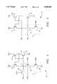
- FIG. 1ashows a first version of a non-volatile cell including a cross-coupled latch according to the invention herein;
- FIG. 1bshows a second version of a non-volatile cell including a cross-coupled latch according to the invention herein;
- FIG. 2shows a variation of the non-volatile cell according to the invention herein with a single bitline connection and with a reduced number of transistors.
- FIG. 3shows yet another variation of the non-volatile cell according to the invention herein;
- FIG. 4shows a multicell arrangement of non-volatile cells according to the invention herein;
- FIG. 5shows the arrangement of FIG. 4 further including transistors for enabling the programming of selected cells of the invention.
- FIG. 6shows a variation of the arrangement of FIG. 5 which permits programming of selected cells of the programmable circuit device of the invention.
- FIG. 1ashows a self-sensing non-volatile cell 10 according to the invention herein including first and second latch (e.g., p-channel enhancement) pull-up transistors respectively 12 and 14, connected at their respective sources to multiple voltage VM as a supply voltage.
- VMcan be set to a selected voltage, including VCC or a higher level, e.g. VPP, for programming.
- Pull-up transistors 12 and 14are cross-coupled as a latch, by electrically connecting their respective control gates to each other's drains at respective terminal nodes A and B, as shown in FIG. 1a.
- FIG. 1ashows a self-sensing non-volatile cell 10 according to the invention herein including first and second latch (e.g., p-channel enhancement) pull-up transistors respectively 12 and 14, connected at their respective sources to multiple voltage VM as a supply voltage.
- VMcan be set to a selected voltage, including VCC or a higher level, e.g. VPP, for
- terminal nodes A and Bare in turn connected respectively to non-volatile subcells 15a and 15b respectively including (e.g., n-channel enhancement) pull-down transistors 16 and 18.
- terminal nodes A and Bcan alternatively each be connected directly to a single-transistor cell, without the need for pull-down transistors 16 and 18.
- FIG. 1aadditionally shows self-sensing non-volatile cell 10 including first and second enhancement transistors 20 and 21 connected respectively to terminal nodes A and B and respective bitlines BL1 and BL2.
- Enhancement transistors 20 and 21are clocked by wordline W/L.
- Non-volatile subcells 15a and 15beach include first and second floating-gate n-channel depletion transistors 24 and 25 respectively connected in series to pull-down transistors 16 and 18.
- the drain of floating-gate transistor 24is connected to the source of pull-down transistor 16.
- the drain of floating-gate transistor 25is connected to the source of pull-down transistor 18.
- the drains of respective pull-down transistors 16 and 18are respectively connected to terminal nodes A and B.
- non-volatile cell 10may be read or programmed at respective bitlines BL1 and BL2 at respective terminal nodes A and B.
- Non-volatile subcell 15ais programmed by setting wordline W/L and bitline BL1 to voltage level VCC, while bitline BL2 is set to zero. Latching of information from bitline BL1 is accomplished by setting programming wordline PWL to VCC at 5 volts. Once the information from bitline BL1 has been stored in subcell 15a, and particularly in floating-gate transistor 24, supply voltage VM is pumped up to higher voltage level VPP. Programming wordline PWL is also set high to VPP. Accordingly, terminal node A goes to VPP, and terminal node B remains at ground.
- non-volatile cell 15ais programmed, and the other non-volatile cell 15b is set to a complementary state by action of cross-latched pull-up transistors 12 and 14. Accordingly, when floating-gate transistor 24 is set high, floating gate transistor 25 will be latched low.
- Non-volatile subcell 15acan be read by setting programming wordline PWL below VCC and REF at a selected constant voltage level sufficient to permit activation. Access to non-volatile subcell 15a is thus accomplished by setting wordline W/L to 5 volts, enabling data to be read at both bitline BL1 and bitline BL2 to produce a differential output.
- FIG. 1bshows another version of the invention in which pull-down transistors 16 and 18 are eliminated. This can be done by using n-channel enhancement floating-gate transistors 24 and 25 rather than n-channel depletion transistors. Accordingly, floating-gate transistors 24 and 25 can be driven at their respective gates by programming wordline PWL directly. Otherwise, the circuitry of FIG. 1B and its general operation tracks that of the circuitry in FIG. 1a.
- FIG. 2shows a variation of non-volatile cell 10 according to the invention herein with a single bit-line B/L connection and with a reduced number of transistors and only a single non-volatile subcell 15 including pull-down transistor 16 and floating-gate transistor 24.
- FIG. 2shows non-volatile cell 10 including first and second p-channel enhancement pull-up transistors respectively 12 and 14, connected at their respective sources to VM.
- depletion channel transistorsmay be employed.
- Pull-up transistors 12 and 14are cross-coupled as a latch, by electrically connecting their respective control gates to each other's drains at respective terminal nodes A and B. Terminal node A is in turn connected to pull-down transistor 16.
- Node terminal Bis connected to pull-down enhancement transistor 18 at its drain.
- FIG. 2additionally shows non-volatile cell 10 including a single enhancement transistor 20 connected to node A.
- Non-volatile cell 10further includes n-channel depletion floating-gate transistor 24 connected to pull-down transistor 16. Further, the drain of floating-gate transistor 24 is connected to the source of pull-down transistor 16, and the drain of pull-down transistor 16 is connected to terminal node A. The control gate of pull-down transistor 18 is additionally connected to terminal node A, and its source is grounded.
- Enhancement transistor 20is clocked by wordline W/L. As clocked, non-volatile cell 10 is connected with bitline B/L at node terminal A.
- Non-volatile subcell 15is programmable by selecting wordline W/L and bitline B/L to have the value of VCC.
- Latching of data onto non-volatile subcell 15 from bitline B/Lis accomplished by setting programming wordline PWL to VCC at 5 volts. Once the data from B/L has been latched onto pull-down transistor 16, VM is pumped up to VPP. Programming wordline PWL is also set high to VPP. Accordingly, node terminal A goes to VPP. In summary, according to this programming approach, floating gate transistor 24 is programmed.
- Non-volatile subcell 15can be read by setting positive wordline PWL below VCC and Ref at a selected constant voltage level. Access to non-volatile subcell 15 is accomplished by setting wordline W/L to 5 volts, enabling data to be read at bitline B/L. The arrangement of FIG. 2 is useful where a differential output along two bitlines is not required.
- FIG. 3shows a second variation of self-sensing, non-volatile cell 10 according to the invention herein, with a wordline W/L controlling pull-down transistors 16 and 18.
- Pull-up transistors 12 and 14remain connected as in FIGS. 1A and 1B, and pull-down transistors 16 and 18 are connected as before to respective pull-up transistors 12 and 14.
- floating-gate transistor 24is connected to the source of pull-down transistor 16.
- the gates of transistors 16 and 18are connected and driven by wordline W/L.
- Pull-down transistor 18further has its source grounded. Bitline B/L is thus connected to floating-gate transistor 24 for reading and programming in accordance with control signals on wordline W/L.
- floating-gate transistor 24 shownis an n-channel depletion transistor.
- pull-down transistor 16can be eliminated by using a p-channel enhancement floating-gate transistor 24.
- pull-up transistors 12 and 14permit reduced power reading and programming operations. Power requirements can be further reduced to produce a zero-power arrangement, as shown in FIG. 2, by shutting off transistor 14 when transistor 12 is on (and vice-versa), by connecting the control gates of pull-up transistor 14 and pull-down transistor 18.
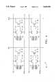
- FIG. 4shows a non-volatile multicell arrangement 40 of eight non-volatile self-sensing cells 10 according to the invention herein.
- Multicell arrangement 40is either zero power or low power depending upon whether or not exclusively zero power cells are employed.
- Non-volatile cells 10are paired or multiplexed and only one of self-sensing cells SSC1 and SSC2 is selected at any given time. Additional pairs of multiplexed cells include SSC3 and SSC4; SSC5 and SSC6; and SSC7 and SSC8.
- Multicell arrangement 40 shown in FIG. 4includes four such paired groupings of cells 10. Each grouping of multiplexed SSC cells further includes a pair of input lines associated with a single bitline BL.
- the first grouping of cells 10 in multicell arrangement 40includes, for example, input lines, IT1 and IT1%, bitline BL1, first and second self-sensing non-volatile cells 10, SSC1 and SSC2, first and second input line selection transistors 43 and 44, and bitline transistor 45.
- the eight cell arrangement of FIG. 4provides for two pairs of input lines for selecting which one of each pair of cells 10 is to be asserted at any given time, and two output bitlines BL1 and BL2.
- the input linesinclude IT1, IT1%, IT2, and IT2%.
- IT1 and IT1%form a first pair of input lines which carry complementary signals to ensure that only one of input line selection transistors 43 and 44 is selected at any given time.
- IT2 and IT2%form a second pair of input lines effective for controlling the selection of a self-sensing cell 10 from another paired group.
- IT1is high, the data from SSC1 will turn transistor 45 in its grouping on or off depending on the logical state of cell SSC1.
- bitlines BL1 and BL2may accordingly implement first and second logical OR functions based upon the input terms produced from two cells 10 controlled by the selection of input line pairs IT1 and IT1%, and IT2 and IT2%.
- arrangement 40can be connected as part of a CMOS logic array of zero-power logic gates, the gates including AND, NAND, OR, NOR, XOR, XNOR, XAND, XNAND, or other kinds of gates, including complex gate arrangements.
- Bitline 45are preferably high-speed single-poly transistors to maximize speed. Self-sensing cells SSC1-SSC8 are disconnected from the speed path of multicell arrangement 40, even though cells 10 do determine the logical states of respective transistors 45.
- FIG. 5shows the arrangement of FIG. 4 further including programming transistors 50 and 51 for enabling the programming of selected self-sensing cells 10 in multicell arrangement 40.
- transistor 50is connected to self-sensing cell SSC1 to enable communication between bitline BL1 and self-sensing cell SSC1 under gate control of an input programming signal P(a1).
- transistor 51is connected to self-sensing cell SSC2 to enable communication between bitline BL1 and self-sensing cell SSC2 under gate control of a second input programming signal P(a2), which controls transistor 44 at its control gate.
- FIG. 6shows yet another variation of the arrangement of FIG. 4 which permits programming of selected self-sensing cells 10 of multicell arrangement 40 of the invention.
- transistors 60 and 61are connected to bitline BL1 for programming under control of respective gate programming signals P(a1) and P(a2), while read operations are conducted with reference to bitline BL2 through input line selection transistors 43 and 44, and bitline transistor 45.
- high speed programming and read operationsare accomplished at zero power consumption with programmable circuit devices having non-volatile, self-sensing cells which rely upon cross-coupled pull-up latch transistors connected to non-volatile pull-down subcells.
- Zero-power consumptionis passed upon zero DC power conditions and the absence of DC currents in applicable cells or subcells.
- the overall circuitry in which the zero power cells or subcells are connectedmay nonetheless be at low power, allowing for some DC current.
- the self-sensing cells 10 described hereinare considered to be self-sensing in that no sense amplifiers are required for communication of information as to the memory states of the cells. Instead, the self-sensing cells 10 are able to provide a direct logical output for the bitline.
Landscapes
- Engineering & Computer Science (AREA)
- Microelectronics & Electronic Packaging (AREA)
- Logic Circuits (AREA)
- Read Only Memory (AREA)
- Static Random-Access Memory (AREA)
Abstract
Description
Claims (20)
Priority Applications (8)
| Application Number | Priority Date | Filing Date | Title |
|---|---|---|---|
| US08/194,930US5440508A (en) | 1994-02-09 | 1994-02-09 | Zero power high speed programmable circuit device architecture |
| PCT/US1995/001437WO1995022144A1 (en) | 1994-02-09 | 1995-02-02 | Zero power high speed programmable circuit device architecture |
| EP95908799AEP0693217B1 (en) | 1994-02-09 | 1995-02-02 | Zero power high speed programmable circuit device architecture |
| CN95190071ACN1094635C (en) | 1994-02-09 | 1995-02-02 | Zero-power high-speed programmable circuit device structure |
| DE69516761TDE69516761T2 (en) | 1994-02-09 | 1995-02-02 | PROGRAMMABLE HIGH-SPEED SWITCHING ARCHITECTURE WITH LOW POWER CONSUMPTION |
| KR1019950704411AKR100310358B1 (en) | 1994-02-09 | 1995-02-02 | Fast programmable circuit device structure with zero power |
| JP52127095AJP3375134B2 (en) | 1994-02-09 | 1995-02-02 | Zero power high speed programmable circuit device architecture |
| TW084101229ATW269760B (en) | 1994-02-09 | 1995-02-11 |
Applications Claiming Priority (1)
| Application Number | Priority Date | Filing Date | Title |
|---|---|---|---|
| US08/194,930US5440508A (en) | 1994-02-09 | 1994-02-09 | Zero power high speed programmable circuit device architecture |
Publications (1)
| Publication Number | Publication Date |
|---|---|
| US5440508Atrue US5440508A (en) | 1995-08-08 |
Family
ID=22719429
Family Applications (1)
| Application Number | Title | Priority Date | Filing Date |
|---|---|---|---|
| US08/194,930Expired - LifetimeUS5440508A (en) | 1994-02-09 | 1994-02-09 | Zero power high speed programmable circuit device architecture |
Country Status (8)
| Country | Link |
|---|---|
| US (1) | US5440508A (en) |
| EP (1) | EP0693217B1 (en) |
| JP (1) | JP3375134B2 (en) |
| KR (1) | KR100310358B1 (en) |
| CN (1) | CN1094635C (en) |
| DE (1) | DE69516761T2 (en) |
| TW (1) | TW269760B (en) |
| WO (1) | WO1995022144A1 (en) |
Cited By (15)
| Publication number | Priority date | Publication date | Assignee | Title |
|---|---|---|---|---|
| US5592417A (en)* | 1994-01-31 | 1997-01-07 | Sgs-Thomson Microelectronics S.A. | Non-volatile programmable bistable multivibrator, programmable by the source, for memory redundancy circuit |
| US5640342A (en)* | 1995-11-20 | 1997-06-17 | Micron Technology, Inc. | Structure for cross coupled thin film transistors and static random access memory cell |
| US5805496A (en)* | 1996-12-27 | 1998-09-08 | International Business Machines Corporation | Four device SRAM cell with single bitline |
| US6469930B1 (en) | 2000-10-30 | 2002-10-22 | Cypress Semiconductor Corporation | Compact nonvolatile circuit having margin testing capability |
| US6556487B1 (en) | 2000-09-20 | 2003-04-29 | Cypress Semiconductor Corp. | Non-volatile static memory cell |
| US6809550B2 (en) | 2002-09-20 | 2004-10-26 | Atmel Corporation | High speed zero DC power programmable logic device (PLD) architecture |
| KR100789517B1 (en)* | 2000-06-14 | 2007-12-28 | 가부시키가이샤 히타치세이사쿠쇼 | Semiconductor devices |
| US20080025091A1 (en)* | 2004-09-09 | 2008-01-31 | Actel Corporation | Non-volatile memory cells in a field programmable gate array |
| KR100812520B1 (en) | 2007-02-06 | 2008-03-11 | 매그나칩 반도체 유한회사 | Semiconductor memory device |
| US20090168520A1 (en)* | 2007-12-31 | 2009-07-02 | Simtek | 3T high density NVDRAM cell |
| US20090168519A1 (en)* | 2007-12-31 | 2009-07-02 | Simtek | Architecture of a nvDRAM array and its sense regime |
| US20090168521A1 (en)* | 2007-12-31 | 2009-07-02 | Simtek | 5T high density NVDRAM cell |
| US7581117B1 (en) | 2005-07-19 | 2009-08-25 | Actel Corporation | Method for secure delivery of configuration data for a programmable logic device |
| US7821859B1 (en) | 2006-10-24 | 2010-10-26 | Cypress Semiconductor Corporation | Adaptive current sense amplifier with direct array access capability |
| US8072834B2 (en) | 2005-08-25 | 2011-12-06 | Cypress Semiconductor Corporation | Line driver circuit and method with standby mode of operation |
Families Citing this family (6)
| Publication number | Priority date | Publication date | Assignee | Title |
|---|---|---|---|---|
| JP2000123591A (en)* | 1998-10-16 | 2000-04-28 | Fujitsu Ltd | Nonvolatile semiconductor memory device |
| WO2004086512A1 (en)* | 2003-03-26 | 2004-10-07 | Fujitsu Limited | Semiconductor memory |
| US7369111B2 (en) | 2003-04-29 | 2008-05-06 | Samsung Electronics Co., Ltd. | Gate driving circuit and display apparatus having the same |
| JP2006527897A (en) | 2003-06-17 | 2006-12-07 | コーニンクレッカ フィリップス エレクトロニクス エヌ ヴィ | Nonvolatile static memory cell |
| WO2005096314A1 (en)* | 2004-03-31 | 2005-10-13 | Kitakyushu Foundation For The Advancement Of Industry, Science And Technology | Semiconductor nonvolatile storage circuit |
| JP5330435B2 (en)* | 2011-03-15 | 2013-10-30 | 株式会社東芝 | Non-volatile configuration memory |
Citations (4)
| Publication number | Priority date | Publication date | Assignee | Title |
|---|---|---|---|---|
| US4914318A (en)* | 1988-12-30 | 1990-04-03 | Intel Corporation | Latch circuit for a programmable logic device using dual n-type transistors |
| US5065362A (en)* | 1989-06-02 | 1991-11-12 | Simtek Corporation | Non-volatile ram with integrated compact static ram load configuration |
| US5079450A (en)* | 1988-12-16 | 1992-01-07 | Advance Micro Devices, Inc. | Self-latching logic gate for use in programmable logic array circuits |
| US5210448A (en)* | 1990-06-13 | 1993-05-11 | Ricoh Company, Ltd. | Programmable logic device |
Family Cites Families (6)
| Publication number | Priority date | Publication date | Assignee | Title |
|---|---|---|---|---|
| US4132904A (en)* | 1977-07-28 | 1979-01-02 | Hughes Aircraft Company | Volatile/non-volatile logic latch circuit |
| US4460978A (en)* | 1981-11-19 | 1984-07-17 | Mostek Corporation | Nonvolatile static random access memory cell |
| US4980859A (en)* | 1989-04-07 | 1990-12-25 | Xicor, Inc. | NOVRAM cell using two differential decouplable nonvolatile memory elements |
| US5270587A (en)* | 1992-01-06 | 1993-12-14 | Micron Technology, Inc. | CMOS logic cell for high-speed, zero-power programmable array logic devices |
| DE4342821C1 (en)* | 1993-12-15 | 1994-12-15 | Sgs Thomson Microelectronics | Electronic memory circuit |
| FR2715759B1 (en)* | 1994-01-31 | 1996-03-22 | Sgs Thomson Microelectronics | Programmable non-volatile flip-flop with noise reduction in read mode, especially for memory redundancy circuit. |
- 1994
- 1994-02-09USUS08/194,930patent/US5440508A/ennot_activeExpired - Lifetime
- 1995
- 1995-02-02JPJP52127095Apatent/JP3375134B2/ennot_activeExpired - Fee Related
- 1995-02-02DEDE69516761Tpatent/DE69516761T2/ennot_activeExpired - Lifetime
- 1995-02-02WOPCT/US1995/001437patent/WO1995022144A1/enactiveIP Right Grant
- 1995-02-02KRKR1019950704411Apatent/KR100310358B1/ennot_activeExpired - Fee Related
- 1995-02-02EPEP95908799Apatent/EP0693217B1/ennot_activeExpired - Lifetime
- 1995-02-02CNCN95190071Apatent/CN1094635C/ennot_activeExpired - Fee Related
- 1995-02-11TWTW084101229Apatent/TW269760B/zhnot_activeIP Right Cessation
Patent Citations (4)
| Publication number | Priority date | Publication date | Assignee | Title |
|---|---|---|---|---|
| US5079450A (en)* | 1988-12-16 | 1992-01-07 | Advance Micro Devices, Inc. | Self-latching logic gate for use in programmable logic array circuits |
| US4914318A (en)* | 1988-12-30 | 1990-04-03 | Intel Corporation | Latch circuit for a programmable logic device using dual n-type transistors |
| US5065362A (en)* | 1989-06-02 | 1991-11-12 | Simtek Corporation | Non-volatile ram with integrated compact static ram load configuration |
| US5210448A (en)* | 1990-06-13 | 1993-05-11 | Ricoh Company, Ltd. | Programmable logic device |
Cited By (26)
| Publication number | Priority date | Publication date | Assignee | Title |
|---|---|---|---|---|
| US5721706A (en)* | 1994-01-31 | 1998-02-24 | Sgs-Thomson Microelectronics S.A. | Non-volatile-programmable bistable multivibrator, programmable by the source, for memory redundancy circuit |
| US5592417A (en)* | 1994-01-31 | 1997-01-07 | Sgs-Thomson Microelectronics S.A. | Non-volatile programmable bistable multivibrator, programmable by the source, for memory redundancy circuit |
| US5677870A (en)* | 1994-01-31 | 1997-10-14 | Sgs-Thomson Microelectronics S.A. | Non-volatile programmable bistable multivibrator, programmable by the source, for the memory redundancy circuit |
| US6291276B1 (en) | 1995-11-20 | 2001-09-18 | Micron Technology, Inc. | Cross coupled thin film transistors and static random access memory cell |
| US6054742A (en)* | 1995-11-20 | 2000-04-25 | Micron Technology, Inc. | Structure for cross coupled thin film transistors and static random access memory cell |
| US5640342A (en)* | 1995-11-20 | 1997-06-17 | Micron Technology, Inc. | Structure for cross coupled thin film transistors and static random access memory cell |
| US5805496A (en)* | 1996-12-27 | 1998-09-08 | International Business Machines Corporation | Four device SRAM cell with single bitline |
| KR100789517B1 (en)* | 2000-06-14 | 2007-12-28 | 가부시키가이샤 히타치세이사쿠쇼 | Semiconductor devices |
| US6556487B1 (en) | 2000-09-20 | 2003-04-29 | Cypress Semiconductor Corp. | Non-volatile static memory cell |
| US6469930B1 (en) | 2000-10-30 | 2002-10-22 | Cypress Semiconductor Corporation | Compact nonvolatile circuit having margin testing capability |
| US6809550B2 (en) | 2002-09-20 | 2004-10-26 | Atmel Corporation | High speed zero DC power programmable logic device (PLD) architecture |
| US7430137B2 (en) | 2004-09-09 | 2008-09-30 | Actel Corporation | Non-volatile memory cells in a field programmable gate array |
| US20080025091A1 (en)* | 2004-09-09 | 2008-01-31 | Actel Corporation | Non-volatile memory cells in a field programmable gate array |
| US7581117B1 (en) | 2005-07-19 | 2009-08-25 | Actel Corporation | Method for secure delivery of configuration data for a programmable logic device |
| US8072834B2 (en) | 2005-08-25 | 2011-12-06 | Cypress Semiconductor Corporation | Line driver circuit and method with standby mode of operation |
| US7821859B1 (en) | 2006-10-24 | 2010-10-26 | Cypress Semiconductor Corporation | Adaptive current sense amplifier with direct array access capability |
| US20080186768A1 (en)* | 2007-02-06 | 2008-08-07 | Magnachip Semiconductor, Ltd. | Semiconductor memory device |
| KR100812520B1 (en) | 2007-02-06 | 2008-03-11 | 매그나칩 반도체 유한회사 | Semiconductor memory device |
| US7755943B2 (en) | 2007-02-06 | 2010-07-13 | Magnachip Semiconductor, Ltd. | Unit cell block of EEPROM and semiconductor memory device having the same |
| US20090168520A1 (en)* | 2007-12-31 | 2009-07-02 | Simtek | 3T high density NVDRAM cell |
| US20090168519A1 (en)* | 2007-12-31 | 2009-07-02 | Simtek | Architecture of a nvDRAM array and its sense regime |
| US20090168521A1 (en)* | 2007-12-31 | 2009-07-02 | Simtek | 5T high density NVDRAM cell |
| US8036032B2 (en) | 2007-12-31 | 2011-10-11 | Cypress Semiconductor Corporation | 5T high density NVDRAM cell |
| US8059458B2 (en) | 2007-12-31 | 2011-11-15 | Cypress Semiconductor Corporation | 3T high density nvDRAM cell |
| US8064255B2 (en) | 2007-12-31 | 2011-11-22 | Cypress Semiconductor Corporation | Architecture of a nvDRAM array and its sense regime |
| US8488379B2 (en) | 2007-12-31 | 2013-07-16 | Cypress Semiconductor Corporation | 5T high density nvDRAM cell |
Also Published As
| Publication number | Publication date |
|---|---|
| DE69516761D1 (en) | 2000-06-15 |
| EP0693217B1 (en) | 2000-05-10 |
| JP3375134B2 (en) | 2003-02-10 |
| KR100310358B1 (en) | 2001-12-17 |
| KR960702156A (en) | 1996-03-28 |
| TW269760B (en) | 1996-02-01 |
| JPH08509091A (en) | 1996-09-24 |
| CN1123062A (en) | 1996-05-22 |
| WO1995022144A1 (en) | 1995-08-17 |
| EP0693217A1 (en) | 1996-01-24 |
| DE69516761T2 (en) | 2001-01-25 |
| EP0693217A4 (en) | 1998-09-30 |
| CN1094635C (en) | 2002-11-20 |
Similar Documents
| Publication | Publication Date | Title |
|---|---|---|
| US5440508A (en) | Zero power high speed programmable circuit device architecture | |
| US4094012A (en) | Electrically programmable MOS read-only memory with isolated decoders | |
| US5917753A (en) | Sensing circuitry for reading and verifying the contents of electrically programmable/erasable non-volatile memory cells | |
| US5594687A (en) | Completely complementary MOS memory cell with tunneling through the NMOS and PMOS transistors during program and erase | |
| US5761146A (en) | Data in/out channel control circuit of semiconductor memory device having multi-bank structure | |
| KR100391020B1 (en) | Data holding circuit | |
| EP0136811B1 (en) | Bit line load and column circuitry for a semiconductor memory | |
| US4745579A (en) | Electrically erasable programmable logic array (EEPLA) | |
| JP2782682B2 (en) | Static memory cell | |
| JPH0734311B2 (en) | Memory cell | |
| US5668765A (en) | Charge transfer sense amplifier | |
| US5132933A (en) | Bias circuitry for nonvolatile memory array | |
| EP0434104B1 (en) | Integrated semiconductor circuit of the master slice type | |
| US6097618A (en) | Apparatus and method for correcting data in a non-volatile random access memory | |
| EP0306519B1 (en) | Current sensing differential amplifier | |
| US5243569A (en) | Differential cell-type eprom incorporating stress test circuit | |
| US5748556A (en) | Tristatable driver for internal data bus lines | |
| US5717650A (en) | Row/column decoder circuits for a semiconductor memory device | |
| US5953259A (en) | Integrated circuit memory devices having cross-coupled isolation gate controllers which provide simultaneous reading and writing capability to multiple memory arrays | |
| JPS649680B2 (en) | ||
| US5295104A (en) | Integrated circuit with precharged internal data bus | |
| JPH09185886A (en) | Data holding circuit | |
| US5982692A (en) | Bit line boost amplifier | |
| KR960004737B1 (en) | Semiconductor integrated circuit | |
| EP0547892B1 (en) | An integrated circuit with self-biased differential data lines |
Legal Events
| Date | Code | Title | Description |
|---|---|---|---|
| AS | Assignment | Owner name:ATMEL CORPORATION Free format text:ASSIGNMENT OF ASSIGNORS INTEREST;ASSIGNORS:PATHAK, SAROJ;PAYNE, JAMES E.;REEL/FRAME:007412/0385 Effective date:19940207 | |
| STCF | Information on status: patent grant | Free format text:PATENTED CASE | |
| FPAY | Fee payment | Year of fee payment:4 | |
| AS | Assignment | Owner name:ATMEL CORPORATION, CALIFORNIA Free format text:ASSIGNMENT OF ASSIGNORS INTEREST;ASSIGNOR:ATMEL CORPORATION;REEL/FRAME:010231/0283 Effective date:19990913 | |
| FPAY | Fee payment | Year of fee payment:8 | |
| FPAY | Fee payment | Year of fee payment:12 | |
| FEPP | Fee payment procedure | Free format text:PAYOR NUMBER ASSIGNED (ORIGINAL EVENT CODE: ASPN); ENTITY STATUS OF PATENT OWNER: LARGE ENTITY | |
| AS | Assignment | Owner name:MORGAN STANLEY SENIOR FUNDING, INC. AS ADMINISTRATIVE AGENT, NEW YORK Free format text:PATENT SECURITY AGREEMENT;ASSIGNOR:ATMEL CORPORATION;REEL/FRAME:031912/0173 Effective date:20131206 Owner name:MORGAN STANLEY SENIOR FUNDING, INC. AS ADMINISTRAT Free format text:PATENT SECURITY AGREEMENT;ASSIGNOR:ATMEL CORPORATION;REEL/FRAME:031912/0173 Effective date:20131206 | |
| AS | Assignment | Owner name:ATMEL CORPORATION, CALIFORNIA Free format text:TERMINATION AND RELEASE OF SECURITY INTEREST IN PATENT COLLATERAL;ASSIGNOR:MORGAN STANLEY SENIOR FUNDING, INC.;REEL/FRAME:038376/0001 Effective date:20160404 |