US5440247A - Fast CMOS logic with programmable logic control - Google Patents
Fast CMOS logic with programmable logic controlDownload PDFInfo
- Publication number
- US5440247A US5440247AUS08/066,555US6655593AUS5440247AUS 5440247 AUS5440247 AUS 5440247AUS 6655593 AUS6655593 AUS 6655593AUS 5440247 AUS5440247 AUS 5440247A
- Authority
- US
- United States
- Prior art keywords
- logic
- stage
- logic circuit
- input
- circuit stage
- Prior art date
- Legal status (The legal status is an assumption and is not a legal conclusion. Google has not performed a legal analysis and makes no representation as to the accuracy of the status listed.)
- Expired - Lifetime
Links
Images

Classifications
- H—ELECTRICITY
- H03—ELECTRONIC CIRCUITRY
- H03K—PULSE TECHNIQUE
- H03K19/00—Logic circuits, i.e. having at least two inputs acting on one output; Inverting circuits
- H03K19/02—Logic circuits, i.e. having at least two inputs acting on one output; Inverting circuits using specified components
- H03K19/173—Logic circuits, i.e. having at least two inputs acting on one output; Inverting circuits using specified components using elementary logic circuits as components
- H03K19/1733—Controllable logic circuits
- H03K19/1735—Controllable logic circuits by wiring, e.g. uncommitted logic arrays
- H03K19/1736—Controllable logic circuits by wiring, e.g. uncommitted logic arrays in which the wiring can be modified
Definitions
- the present inventionrelates to digital logic circuits, especially CMOS combinatorial logic circuits, and, in particular, to programmable control of such circuits.
- the inventionalso relates to multifunctional or programmable logic circuits and devices.
- FIG. 1a programmable logic device having a programmable AND plane 11 followed by an OR plane with macrocells 13 is shown.
- the devicehas k inputs received by the AND plane 11 and m outputs provided by the OR plane and macrocells 13.
- the OR plane 13itself receives l product term lines from the AND plane 11, and if sequential logic is provided, the device will also have n feedback lines from the macrocells back into the AND plane.
- Macrocells for such programmable logic devicesprovide a number of options related to the device outputs, such as output enable and disable control, inverted or noninverted output signal polarity, stored or nonstored output signals, and selectable output pin utilization by multiple logic array blocks. Further, most macrocells also provide the capability of feeding one or more logic signals back into the programmable AND plane. Examples of typical macrocells are described in U.S. Pat. Nos. 4,124,899; 4,609,986; 4,684,830; 4,717,912; 4,758,746; 4,771,285; 4,789,951; 4,879,481; 4,894,563; and 4,912,345.
- FIG. 2A logic signal representing the result of carrying out a specified function by programmable logic is received on a macrocell input line 12 connected, for example, to an output of an OR gate of the programmable logic.
- the macrocell input 12is connected to a conductive line 14, which in turn has an inverter 15 connected to a side branch of the conductive line 14.
- Macrocell input 12is also connected to an input D of a storage register or flip-flop 16 with complementary outputs Q and Q connected to lines 17 and 18.
- Four versions of the received logic signalare thus derived and presented on inputs 14, 15, 17 and 18 to a multiplexer 19, i.e.
- the multiplexer 19responsive to control signals provided by programmable switches, such as EPROMs, selects one of the four signal variants and transmits that selected signal to its output 20.
- a tristatable driver 22responsive to an output enable signal EN transmits the signal to an input/output pin 24.
- three signalsare presented to the multiplexer 36, which selects one of them for feedback along conductive line 42 to the programmable logic, for example, to an input of a programmable AND array.
- Conductive lines 43 and programmable switches 45a, 45b, etc.can connect pins to an adjacent macrocell for efficient use of pin resources.
- Such programmable logic devicesare highly flexible and capable of being programmed to carry out a large number of possible logic functions, but are normally slow, because the capacitance on the various signal lines and the large number of programmable switches cause delays when signal levels are changed.
- a typical throughput for a programmable logic device made using a 1 ⁇ m CMOS processis about 5.5 ns.
- FIG. 3An example of a conventional hardwired CMOS combinatorial logic circuit, shown in FIG. 3, is significantly faster, with a typical throughput of only 0.75 ns. Such a circuit is fast because it has only a few stages of conventional CMOS logic gates, but it lacks functional flexibility. Similar circuits with logic gates can be given a limited amount of flexibility with nearly the same speed as the fixed function circuit of FIG. 3, by including, for example, one or more multiplexers or by providing logic gates with a programmable number of inputs.
- one or more signalsneed to be operated upon quickly with combinatorial logic that varies too much according to a particular situation or set of conditions or that is too complex for simple hardwired logic gates to handle.
- programmable logic devicesare used for such applications because they are capable of being programmed to carry out any one of a large number of possible logic functions and because they are able to carry out very complex logic.
- such devicesare not especially fast, as already noted, and are generally not able to operate quickly on any signal.
- Even the macrocellswhich could be constructed to receive some inputs directly from external pins for output enable or clocking, and which generally are relatively fast, are not expected to perform any combinatorial logic on signals they receive. Any additional logic needed by such signals are provided by feeding back these signals to the programmable logic via feedback lines in the macrocells.
- An object of the present inventionis to provide digital logic circuit combining the functional flexibility of programmable logic devices and the fast operation of fixed CMOS combinatorial logic to perform flexible logic on a fast input.
- the objectis met by a logic circuit having a programmable first stage and a nonprogrammable, second stage with at least one input to the circuit being supplied directly to the second stage rather than indirectly via the first stage.
- the first stagecan be any kind of programmable, and thus functionally flexible, logic circuit, especially a programmable logic device (PLD). Such functionally flexible circuits are usually relatively slow because of capacitance associated with interconnects or row and column circuitry.
- the second stagecan be any combinatorial logic circuit with CMOS logic gates hardwired to carry out some fixed logic function.
- the second stagecould be a new type of dedicated macrocell for a PLD which is capable of performing combinatorial logic on directly received input signals instead of, or in addition to, the output options provided by ordinary macrocells.
- Combinatorial logic circuitsgenerally have logic gates selected from AND, NAND, OR, NOR, XOR and XNOR gates, with two or more sequential groups of such gates arranged so as to carry out a function that can be set forth in sum-of-products form or its equivalent. Such gates would have low capacitance compared to the first stage and so the second stage would be faster than the first.
- the programmable logic of the first stageserves to control the action of the fixed CMOS logic of the second stage, such that inputs supplied directly to the second stage are quickly operated on by the second stage with a degree of flexibility provided by the controlling action of the first stage.
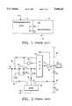
- FIG. 1is a schematic diagram of a programmable logic device of the prior art.
- FIG. 2is a schematic diagram of a typical macrocell unit for the prior art programmable logic device of FIG. 1.
- FIG. 3is a schematic gate level diagram of a typical example of a hardwired CMOS combinatorial logic circuit of the prior art.
- FIG. 4is a schematic diagram of a logic circuit embodiment constructed in accordance with the present invention.
- an example of a logic circuit constructed in accord with the present inventionhas a programmable, but slow, first stage 21 connected to a fixed, but fast, second stage 23 with at least one input 25 directly connected to the second stage 23 rather than connected indirectly via the first stage 21.
- the two stages 21 and 23can be on separate chips or may be integrated on the same chip.
- the second stage 23could be considered to be a special kind of macrocell for the programmable logic of the first stage 21 that differs from the usual output macrocells 23a that just provide output and feedback options for signals provided by the programmable logic 21.
- the first stage 21has multiple inputs 27, which can also include an input line 29 from one or more of the inputs 25 that are directly connected to the second stage 23.
- the first stage 21has outputs 31-34, at least some of which are connected as inputs to the second stage 23.
- the first stage 21can be any sort of programmable logic circuit with a significant amount of functional flexibility comparable to that provided by programmable logic devices (PLDs). However, preferably, the first stage 21 will in fact be a programmable logic device with a programmable AND plane followed by an OR plane and macrocells 23a. Examples of such devices include those commonly known as PALs, PLAs and MFLAs. PALs use a fixed array of OR gates for their OR plane, while PLAs use crossing product term lines and sum term lines interconnectable with programmable switches as their OR plane. PLAs, while more flexible than PALs, are also slower. MFLAs use arrays of addressable multibit storage registers connected to logic gates for at least one of their logic planes. Any of the devices may include storage registers in the macrocells 23a, as well as feedback lines from the macrocells 23a back into the programmable AND plane.
- PLDsprogrammable logic devices
- the second stage 23can be any combinatorial logic circuit with CMOS logic gates hardwired to carry out some fixed logic function.
- the functioncan then be implemented using CMOS logic gates selected from AND, NAND, OR, NOR, XOR and XNOR gates.
- the function F given aboveis implemented in FIG. 3 with two AND gates and a NOR gate. It might also be implemented with two NAND gates and an AND gate as per the derived equivalent form of the function given above.
- NOR gateNOR gate
- FIG. 3there is a group of two AND gates followed by a group of one NOR gate.
- the output of the NOR gateis provided to output 35' of the logic circuit.
- a first combinatorial macrocell 23 of the second stageincludes a group of two AND gates 37 and 38 followed by a group of one OR gate 39.
- Three inputs 32-34 to this second stage logic 23are received from outputs of the first stage 21 and respectively connected to inputs of logic gates 37-39.
- Another input 25is provided directly to second stage 23 and connected to other inputs of logic gates 37 and 38.
- some logic gate inputsmay be inverted to change their polarity, as in the input 40 to AND gate 38, and that some, but not all, inputs to the second stage 23 can bypass one or more groups of logic gates, as in the input 34 bypassing of the group of AND gates 37 and 38.
- the output of the OR gate 39is provided to the output 35 of the logic circuit.
- One or more of the combinatorial macrocells 23, 23', etc.might also have feedback 42' to the programmable logic 21.
- An example of a use for such two-stage logic circuits of the present inventionis memory access by a microprocessor.
- An address provided by a microprocessormay be decoded by the programmable logic in the first stage 21 of the circuit.
- an address strobe signalis supplied after some delayed time period after the providing of the address.
- the address strobe signalis thus applied to an input 25 that is connected directly to the fast second stage 23 of the logic circuit, bypassing the slower first stage 21.
- 3is one that might be used for the second stage 23' with the input A being connected to the fast input 25' to receive the address strobe signal and the inputs B-D connected to the first stage outputs 32'-34' to receive the decoded or partially decoded address.
- Another applicationmight require that a signal received by the fast input 25 to the second logic stage 23 be transmitted as is or inverted, with the polarity depending on a complex condition requiring programmable logic 21.
- the first stage 21then controls the polarity of the signal received at the fast input 25.
- Other applicationsmight require a signal received directly by the second logic stage 23 at a fast input 25 be transmitted or blocked according to a complex logic function implemented in the programmable first stage.
- the signals received on the fast input 25could also be input into the first stage logic 21 via an input line 29.
- the programmable logic 21controls the action of the fixed combinatorial logic 23, permitting fast, but functionally flexible, operation on one or more input signals that need to go through the logic quickly.
Landscapes
- Physics & Mathematics (AREA)
- Engineering & Computer Science (AREA)
- Computer Hardware Design (AREA)
- Computing Systems (AREA)
- General Engineering & Computer Science (AREA)
- Mathematical Physics (AREA)
- Logic Circuits (AREA)
Abstract
Description
Claims (1)
Priority Applications (1)
| Application Number | Priority Date | Filing Date | Title |
|---|---|---|---|
| US08/066,555US5440247A (en) | 1993-05-26 | 1993-05-26 | Fast CMOS logic with programmable logic control |
Applications Claiming Priority (1)
| Application Number | Priority Date | Filing Date | Title |
|---|---|---|---|
| US08/066,555US5440247A (en) | 1993-05-26 | 1993-05-26 | Fast CMOS logic with programmable logic control |
Publications (1)
| Publication Number | Publication Date |
|---|---|
| US5440247Atrue US5440247A (en) | 1995-08-08 |
Family
ID=22070243
Family Applications (1)
| Application Number | Title | Priority Date | Filing Date |
|---|---|---|---|
| US08/066,555Expired - LifetimeUS5440247A (en) | 1993-05-26 | 1993-05-26 | Fast CMOS logic with programmable logic control |
Country Status (1)
| Country | Link |
|---|---|
| US (1) | US5440247A (en) |
Cited By (5)
| Publication number | Priority date | Publication date | Assignee | Title |
|---|---|---|---|---|
| US5502402A (en)* | 1995-01-05 | 1996-03-26 | Texas Instruments Incorporated | FPGA architecture based on a single configurable logic module |
| US5594367A (en)* | 1995-10-16 | 1997-01-14 | Xilinx, Inc. | Output multiplexer within input/output circuit for time multiplexing and high speed logic |
| US5636368A (en)* | 1994-12-23 | 1997-06-03 | Xilinx, Inc. | Method for programming complex PLD having more than one function block type |
| US5684744A (en)* | 1995-12-11 | 1997-11-04 | Hewlett-Packard Company | Configurable multifunction flip-flop |
| US6897681B2 (en)* | 2002-03-27 | 2005-05-24 | Texas Instruments Incorporated | Time division multiplexed serial bus with increased bandwidth |
Citations (19)
| Publication number | Priority date | Publication date | Assignee | Title |
|---|---|---|---|---|
| US4124899A (en)* | 1977-05-23 | 1978-11-07 | Monolithic Memories, Inc. | Programmable array logic circuit |
| US4503387A (en)* | 1982-12-30 | 1985-03-05 | Harris Corporation | A.C. Testing of logic arrays |
| US4525641A (en)* | 1982-12-10 | 1985-06-25 | International Business Machines Corporation | Flip-flop programmer using cascaded logic arrays |
| US4609986A (en)* | 1984-06-14 | 1986-09-02 | Altera Corporation | Programmable logic array device using EPROM technology |
| US4652777A (en)* | 1984-12-18 | 1987-03-24 | Cline Ronald L | CMOS programmable logic array |
| US4684830A (en)* | 1985-03-22 | 1987-08-04 | Monolithic Memories, Inc. | Output circuit for a programmable logic array |
| US4717912A (en)* | 1982-10-07 | 1988-01-05 | Advanced Micro Devices, Inc. | Apparatus for producing any one of a plurality of signals at a single output |
| US4758756A (en)* | 1984-04-13 | 1988-07-19 | Alsthom-Atlantique | Vernier-type electrodynamic machine |
| US4771285A (en)* | 1985-11-05 | 1988-09-13 | Advanced Micro Devices, Inc. | Programmable logic cell with flexible clocking and flexible feedback |
| US4789951A (en)* | 1986-05-16 | 1988-12-06 | Advanced Micro Devices, Inc. | Programmable array logic cell |
| US4833349A (en)* | 1987-09-01 | 1989-05-23 | Plx Technology | Programmable logic and driver circuits |
| US4857773A (en)* | 1985-09-06 | 1989-08-15 | Ricoh Co., Ltd. | Programming logic device with test-signal enabled output |
| US4879481A (en)* | 1988-09-02 | 1989-11-07 | Cypress Semiconductor Corporation | Dual I/O macrocell for high speed synchronous state machine |
| US4894563A (en)* | 1988-10-11 | 1990-01-16 | Atmel Corporation | Output macrocell for programmable logic device |
| US4912345A (en)* | 1988-12-29 | 1990-03-27 | Sgs-Thomson Microelectronics, Inc. | Programmable summing functions for programmable logic devices |
| US4965372A (en)* | 1989-01-19 | 1990-10-23 | Pfizer Inc. | Process and intermediates for isopropyl 3S-amino-2R-hydroxy-alkanoates |
| US5099150A (en)* | 1989-09-29 | 1992-03-24 | Sgs-Thomson Microelectronics, Inc. | Circuit block for programmable logic devices, configurable as a user-writable memory or a logic circuit |
| US5130574A (en)* | 1991-05-06 | 1992-07-14 | Lattice Semiconductor Corporation | Programmable logic device providing product term sharing and steering to the outputs of the programmable logic device |
| US5168178A (en)* | 1991-08-30 | 1992-12-01 | Intel Corporation | High speed NOR'ing inverting, MUX'ing and latching circuit with temperature compensated output noise control |
- 1993
- 1993-05-26USUS08/066,555patent/US5440247A/ennot_activeExpired - Lifetime
Patent Citations (20)
| Publication number | Priority date | Publication date | Assignee | Title |
|---|---|---|---|---|
| US4124899B1 (en)* | 1977-05-23 | 1987-04-28 | ||
| US4124899A (en)* | 1977-05-23 | 1978-11-07 | Monolithic Memories, Inc. | Programmable array logic circuit |
| US4717912A (en)* | 1982-10-07 | 1988-01-05 | Advanced Micro Devices, Inc. | Apparatus for producing any one of a plurality of signals at a single output |
| US4525641A (en)* | 1982-12-10 | 1985-06-25 | International Business Machines Corporation | Flip-flop programmer using cascaded logic arrays |
| US4503387A (en)* | 1982-12-30 | 1985-03-05 | Harris Corporation | A.C. Testing of logic arrays |
| US4758756A (en)* | 1984-04-13 | 1988-07-19 | Alsthom-Atlantique | Vernier-type electrodynamic machine |
| US4609986A (en)* | 1984-06-14 | 1986-09-02 | Altera Corporation | Programmable logic array device using EPROM technology |
| US4652777A (en)* | 1984-12-18 | 1987-03-24 | Cline Ronald L | CMOS programmable logic array |
| US4684830A (en)* | 1985-03-22 | 1987-08-04 | Monolithic Memories, Inc. | Output circuit for a programmable logic array |
| US4857773A (en)* | 1985-09-06 | 1989-08-15 | Ricoh Co., Ltd. | Programming logic device with test-signal enabled output |
| US4771285A (en)* | 1985-11-05 | 1988-09-13 | Advanced Micro Devices, Inc. | Programmable logic cell with flexible clocking and flexible feedback |
| US4789951A (en)* | 1986-05-16 | 1988-12-06 | Advanced Micro Devices, Inc. | Programmable array logic cell |
| US4833349A (en)* | 1987-09-01 | 1989-05-23 | Plx Technology | Programmable logic and driver circuits |
| US4879481A (en)* | 1988-09-02 | 1989-11-07 | Cypress Semiconductor Corporation | Dual I/O macrocell for high speed synchronous state machine |
| US4894563A (en)* | 1988-10-11 | 1990-01-16 | Atmel Corporation | Output macrocell for programmable logic device |
| US4912345A (en)* | 1988-12-29 | 1990-03-27 | Sgs-Thomson Microelectronics, Inc. | Programmable summing functions for programmable logic devices |
| US4965372A (en)* | 1989-01-19 | 1990-10-23 | Pfizer Inc. | Process and intermediates for isopropyl 3S-amino-2R-hydroxy-alkanoates |
| US5099150A (en)* | 1989-09-29 | 1992-03-24 | Sgs-Thomson Microelectronics, Inc. | Circuit block for programmable logic devices, configurable as a user-writable memory or a logic circuit |
| US5130574A (en)* | 1991-05-06 | 1992-07-14 | Lattice Semiconductor Corporation | Programmable logic device providing product term sharing and steering to the outputs of the programmable logic device |
| US5168178A (en)* | 1991-08-30 | 1992-12-01 | Intel Corporation | High speed NOR'ing inverting, MUX'ing and latching circuit with temperature compensated output noise control |
Cited By (7)
| Publication number | Priority date | Publication date | Assignee | Title |
|---|---|---|---|---|
| US5636368A (en)* | 1994-12-23 | 1997-06-03 | Xilinx, Inc. | Method for programming complex PLD having more than one function block type |
| US5963048A (en)* | 1994-12-23 | 1999-10-05 | Xilinx, Inc. | Method for programming complex PLD having more than one function block type |
| US5502402A (en)* | 1995-01-05 | 1996-03-26 | Texas Instruments Incorporated | FPGA architecture based on a single configurable logic module |
| US5594367A (en)* | 1995-10-16 | 1997-01-14 | Xilinx, Inc. | Output multiplexer within input/output circuit for time multiplexing and high speed logic |
| US5684744A (en)* | 1995-12-11 | 1997-11-04 | Hewlett-Packard Company | Configurable multifunction flip-flop |
| US5818273A (en)* | 1995-12-11 | 1998-10-06 | Hewlett-Packard Company | Configurable multifunction flip-flop |
| US6897681B2 (en)* | 2002-03-27 | 2005-05-24 | Texas Instruments Incorporated | Time division multiplexed serial bus with increased bandwidth |
Similar Documents
| Publication | Publication Date | Title |
|---|---|---|
| US5357153A (en) | Macrocell with product-term cascade and improved flip flop utilization | |
| US5341044A (en) | Flexible configuration logic array block for programmable logic devices | |
| US5473266A (en) | Programmable logic device having fast programmable logic array blocks and a central global interconnect array | |
| US4903223A (en) | Programmable logic device with programmable word line connections | |
| US5835998A (en) | Logic cell for programmable logic devices | |
| US5986465A (en) | Programmable logic integrated circuit architecture incorporating a global shareable expander | |
| US6034540A (en) | Programmable logic integrated circuit architecture incorporating a lonely register | |
| US6989689B2 (en) | Interconnection and input/output resources for programmable logic integrated circuit devices | |
| US5399922A (en) | Macrocell comprised of two look-up tables and two flip-flops | |
| US5300830A (en) | Programmable logic device macrocell with an exclusive feedback and exclusive external input lines for registered and combinatorial modes using a dedicated product term for control | |
| US5859542A (en) | Programmable logic array integrated circuits with enhanced cascade | |
| US4963770A (en) | Programmable logic device | |
| US5359242A (en) | Programmable logic with carry-in/carry-out between logic blocks | |
| US5883526A (en) | Hierarchical interconnect for programmable logic devices | |
| US6873182B2 (en) | Programmable logic devices having enhanced cascade functions to provide increased flexibility | |
| US6864714B2 (en) | PLDs providing reduced delays in cascade chain circuits | |
| US5386155A (en) | Apparatus and method for selecting polarity and output type in a programmable logic device | |
| US5053646A (en) | Programmable logic device having expanded logic capability | |
| US5235221A (en) | Field programmable logic array with speed optimized architecture | |
| US5440247A (en) | Fast CMOS logic with programmable logic control | |
| US5384500A (en) | Programmable logic device macrocell with an exclusive feedback and an exclusive external input line for a combinatorial mode and accommodating two separate programmable or planes | |
| US5298803A (en) | Programmable logic device having low power microcells with selectable registered and combinatorial output signals | |
| US7417455B2 (en) | Programmable function generator and method operating as combinational, sequential and routing cells | |
| US6384629B2 (en) | High-speed programmable interconnect | |
| US5936425A (en) | Tri-statable input/output circuitry for programmable logic |
Legal Events
| Date | Code | Title | Description |
|---|---|---|---|
| STPP | Information on status: patent application and granting procedure in general | Free format text:APPLICATION UNDERGOING PREEXAM PROCESSING | |
| FPAY | Fee payment | Year of fee payment:4 | |
| FEPP | Fee payment procedure | Free format text:PETITION RELATED TO MAINTENANCE FEES FILED (ORIGINAL EVENT CODE: PMFP); ENTITY STATUS OF PATENT OWNER: LARGE ENTITY | |
| FEPP | Fee payment procedure | Free format text:PETITION RELATED TO MAINTENANCE FEES GRANTED (ORIGINAL EVENT CODE: PMFG); ENTITY STATUS OF PATENT OWNER: LARGE ENTITY | |
| REMI | Maintenance fee reminder mailed | ||
| AS | Assignment | Owner name:KAPLINSKY, VESSELINA (THE KAPLINSKY REVOCABLE LIVI Free format text:ASSIGNMENT OF ASSIGNORS INTEREST;ASSIGNOR:KAPLINSKY, CECIL H.;REEL/FRAME:014972/0107 Effective date:19991106 Owner name:KAPLINSKY, CECIL H. (THE KAPLINSKY REVOCABLE LIVIN Free format text:ASSIGNMENT OF ASSIGNORS INTEREST;ASSIGNOR:KAPLINSKY, CECIL H.;REEL/FRAME:014972/0107 Effective date:19991106 | |
| REIN | Reinstatement after maintenance fee payment confirmed | ||
| AS | Assignment | Owner name:SAMSUNG ELECTRONICS CO., LTD., KOREA, REPUBLIC OF Free format text:ASSIGNMENT OF ASSIGNORS INTEREST;ASSIGNORS:CECIL H. KAPLINSKY BY PASS TRUST DATED NOVEMBER 11, 1999;VESSELINA KAPLINSKY MARITAL TRUST, THE DATED NOVEMBER 11, 19991;REEL/FRAME:014484/0239 Effective date:20030730 Owner name:VESSELINA KAPLINSKY MARITAL TRUST DATED NOVEMBER 1 Free format text:ASSIGNMENT OF ASSIGNORS INTEREST;ASSIGNOR:KAPLINSKY REVOCABLE LIVING TRUST DATED SEPTEMBER 15, 1999, THE;REEL/FRAME:014515/0178 Effective date:20030730 Owner name:CECIL H. KAPLINSKY BYPASS TRUST DATED NOVEMBER 11, Free format text:ASSIGNMENT OF ASSIGNORS INTEREST;ASSIGNOR:KAPLINSKY REVOCABLE LIVING TRUST DATED SEPTEMBER 15, 1999, THE;REEL/FRAME:014515/0178 Effective date:20030730 | |
| FP | Lapsed due to failure to pay maintenance fee | Effective date:20030808 | |
| FPAY | Fee payment | Year of fee payment:8 | |
| SULP | Surcharge for late payment | ||
| PRDP | Patent reinstated due to the acceptance of a late maintenance fee | Effective date:20031112 | |
| FEPP | Fee payment procedure | Free format text:PAYOR NUMBER ASSIGNED (ORIGINAL EVENT CODE: ASPN); ENTITY STATUS OF PATENT OWNER: LARGE ENTITY | |
| FEPP | Fee payment procedure | Free format text:PAT HOLDER NO LONGER CLAIMS SMALL ENTITY STATUS, ENTITY STATUS SET TO UNDISCOUNTED (ORIGINAL EVENT CODE: STOL); ENTITY STATUS OF PATENT OWNER: LARGE ENTITY | |
| REFU | Refund | Free format text:REFUND - PAYMENT OF MAINTENANCE FEE, 12TH YR, SMALL ENTITY (ORIGINAL EVENT CODE: R2553); ENTITY STATUS OF PATENT OWNER: LARGE ENTITY | |
| FPAY | Fee payment | Year of fee payment:12 | |
| SULP | Surcharge for late payment | Year of fee payment:11 |