US5439840A - Method of forming a nonvolatile random access memory capacitor cell having a metal-oxide dielectric - Google Patents
Method of forming a nonvolatile random access memory capacitor cell having a metal-oxide dielectricDownload PDFInfo
- Publication number
- US5439840A US5439840AUS08/100,793US10079393AUS5439840AUS 5439840 AUS5439840 AUS 5439840AUS 10079393 AUS10079393 AUS 10079393AUS 5439840 AUS5439840 AUS 5439840A
- Authority
- US
- United States
- Prior art keywords
- forming
- metal
- opening
- doped region
- layer
- Prior art date
- Legal status (The legal status is an assumption and is not a legal conclusion. Google has not performed a legal analysis and makes no representation as to the accuracy of the status listed.)
- Expired - Fee Related
Links
Images


Classifications
- H—ELECTRICITY
- H10—SEMICONDUCTOR DEVICES; ELECTRIC SOLID-STATE DEVICES NOT OTHERWISE PROVIDED FOR
- H10B—ELECTRONIC MEMORY DEVICES
- H10B12/00—Dynamic random access memory [DRAM] devices
- H—ELECTRICITY
- H10—SEMICONDUCTOR DEVICES; ELECTRIC SOLID-STATE DEVICES NOT OTHERWISE PROVIDED FOR
- H10B—ELECTRONIC MEMORY DEVICES
- H10B12/00—Dynamic random access memory [DRAM] devices
- H10B12/30—DRAM devices comprising one-transistor - one-capacitor [1T-1C] memory cells
- H10B12/31—DRAM devices comprising one-transistor - one-capacitor [1T-1C] memory cells having a storage electrode stacked over the transistor
- H—ELECTRICITY
- H10—SEMICONDUCTOR DEVICES; ELECTRIC SOLID-STATE DEVICES NOT OTHERWISE PROVIDED FOR
- H10D—INORGANIC ELECTRIC SEMICONDUCTOR DEVICES
- H10D1/00—Resistors, capacitors or inductors
- H10D1/60—Capacitors
- H10D1/68—Capacitors having no potential barriers
- H10D1/682—Capacitors having no potential barriers having dielectrics comprising perovskite structures
Definitions
- the present inventionrelates to the field of semiconductor devices, and in particular, to semiconductor devices having capacitors.
- Capacitorsare used in many types of semiconductor devices. Within memory devices, such as a dynamic-random-access memory (DRAM) cell or a nonvolatile-random-access memory (NVRAM) cell, the capacitor acts as a storage capacitor.
- DRAMdynamic-random-access memory
- NVRAMnonvolatile-random-access memory
- Metal-oxide dielectric layersmay be used in storage capacitors for the DRAM or NVRAM cells because the metal-oxide dielectric layers may have a high-permittivity or ferroelectric properties. As used in this specification, high-permittivity means a permittivity higher than the permittivity of silicon dioxide.
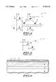
- FIG. 1includes a circuit diagram of an NVRAM cell 1 with a ferroelectric capacitor 2 and a transistor 3.
- One electrode of the ferroelectric capacitor 2is coupled to the drive line (DL), and the other electrode is coupled to a source/drain region of the transistor 3.
- the transistor 3further includes another source/drain region coupled to a bit line (BL) and a gate electrode coupled to a word line (WL).
- One prior art NVRAM cellincludes a "stacked" ferroelectric capacitor.
- the transistoris formed in the substrate, a conductive plug is formed to a source/drain region of the transistor, and the ferroelectric capacitor is formed over the conductive plug.
- An integration problemis the presence of the conductive plug while the ferroelectric capacitor is formed.
- Many types of conductive plugsinclude silicon or a metal-containing material.
- a metal-oxide layer that forms the dielectric layer for the ferroelectric capacitortypically must be oxidized at a temperature higher than about 500 degrees Celsius in order for the metal-oxide layer to have ferroelectric properties. As used in this specification, high temperature means a temperature higher than about 500 degrees Celsius. The conductive plug may not be able to withstand such a processing step.
- the plugmay oxidize to form a region of poor conductivity, thus degrading, or even eliminating, the electrical path between the electrode and the source/drain region of the underlying transistor.
- metal from a metal-containing materialmay diffuse into the substrate.
- the material of the conductive plugmay either form a junction spike or a silicide material that extends completely through the source/drain region causing and electrical short between one of the electrodes of the ferroelectric capacitor and the substrate or a well region.
- barrier layersshould not help because most barrier layers cannot withstand processing higher than about 500 degrees Celsius.
- FIG. 2includes a plan view of a "strapped" NVRAM cell 90 that includes a transistor 93 and a ferroelectric capacitor 95.
- a metal conductor 91acts as a bit line for the NVRAM cell 90 and is electrically connected to a first doped region 931 that acts as a source/drain region by a contact 911.
- Conductive member 92acts as a gate electrode for transistor 93 and is part of the word line.
- a second doped region 932acts as the other source/drain region for the transistor 93 and lies on the other side of the conductive member 92.
- the active region of transistor 93is defined by field isolation region 98.
- a first dielectric layer(not shown) is formed after the transistor 93 is formed and before forming the ferroelectric capacitor 95. Most of the ferroelectric capacitor 95 is typically formed over the field isolation region 98.
- the ferroelectric capacitor 95includes a lower electrode layer 96 that acts as a drive line, a metal-oxide dielectric layer (not shown) that acts as the ferroelectric dielectric, and an upper electrode layer 97.
- a second insulating layer(not shown) is formed over the cell 90.
- Conductive member 94electrically connects the upper electrode layer 97 of the ferroelectric capacitor 95 with the second doped region 932.
- Dashed lines that appear in metal conductor 91 and conductive member 94show where some of the underlying elements of the cell lie below the metal conductor 91 or the conductive member 94. At least one insulating layer lies between the metal conductor 91 or conductive member 94 and those underlying elements indicated by dashed lines. It should be noted that contacts 941, 942, and 911 are typically formed during the same processing steps and that the contacts extend at least through the second insulating layer. It is further noted that the conductive members 91 and 94 are typically formed during the same processing steps, too.
- NVRAM cell 90is very large.
- the cell sizeis limited by how close the conductive members 91 and 94 may be placed to each other and/or how close contacts 941, 942, and 911 may be placed to one another. Further, the cell size is kept large because the orientation of the bit lines across the array typically are generally perpendicular to conductive member 92 that acts as the word line. Thus, the length of the conductive member 91 that acts as the bit line for the cell is generally parallel with the conductive member 94 that acts as an electrical strap.
- the transistor and ferroelectric capacitorare formed side by side from a plan view. The ferroelectric capacitor overlies little, if any, of the transistor because enough tolerance must be given, so that contact 942 contacts doped region 932 and does not contact the lower or upper electrode layer 96 of the ferroelectric capacitor 95.
- FIG. 3is a circuit diagram of an NVRAM cell 30 that includes two transistors 31 and 33 and two ferroelectric capacitors 32 and 34.
- One difference between NVRAM cell 30 and NVRAM cell 1is the use of complementary bit lines (BL and BL) as opposed to a single bit line (BL).
- FIG. 4includes a circuit diagram of NVRAM cell 40 that includes two p-channel transistors 47 and 44, two n-channel transistors 42 and 45, and two ferroelectric capacitors 43 and 46.
- a difference between this cell and NVRAM cell 1is the use of complementary bit lines (BL and BL) and complementary word lines (WL and WL). Stacked ferroelectric capacitors used in NVRAM cells 30 and 40 would have process integration problems, and strapped cells would occupy too much substrate area.
- FIG. 5includes a circuit diagram of a DRAM cell 50. Circuit diagrams for a DRAM cell 50 and NVRAM cell 90 are similar.
- the DRAM cell 50includes a transistor 55 and a storage capacitor 56.
- a bit line (BL)is coupled to a source/drain region of transistor 55.
- Transistor 55further includes a gate electrode that is coupled to a word line (WL) and another source/drain region that is coupled to one of the electrodes of the capacitor 56.
- the other electrode of the capacitor 56is coupled to a constant voltage source V C .
- V C for the cell 50may be V SS or half the potential of V DD .
- Smaller design rulesmay limit the amount of capacitance that can be stored by the storage capacitor of the DRAM cell.
- One way to increase the capacitance of the storage capacitor without increasing thicknesses or dimensionsis the use of a high-permittivity dielectric material, such as a metal-oxide dielectric material.
- a storage capacitor with metal-oxide dielectric layersuffers from integration problems similar to the NVRAM cell. Many of the integration problems of metal-oxide dielectric layers are not seen with a conventional silicon-containing dielectric material, such as silicon dioxide and silicon nitride.
- the present inventionincludes a semiconductor device comprising a circuit element, a capacitor, and a conductive member.
- the capacitoroverlies the circuit element and includes a first electrode layer, a metal-oxide dielectric layer that overlies the first electrode, and a second electrode layer that overlies the dielectric layer.
- the conductive memberelectrically connects the circuit element and the second electrode layer to each other and is configured such that the conductive member extends through the first electrode and dielectric layers of the capacitor.
- the present inventionfurther include a method of making the device.
- FIG. 1includes a circuit diagram of an NVRAM cell having one transistor, one ferroelectric capacitor, and a single bit line. (Prior art)
- FIG. 2include a plan view of a strapped NVRAM cell.
- FIG. 3includes a circuit diagram of an NVRAM cell having two transistors, two ferroelectric capacitors, and complementary bit lines. (Prior art)
- FIG. 4includes a circuit diagram of an NVRAM cell having four transistors, two ferroelectric capacitors, complementary bit lines, and complementary word lines. (Prior art)
- FIG. 5includes a circuit diagram of a DRAM cell. (Prior art)
- FIGS. 6-12include cross-sectional views of a portion of a semiconductor substrate illustrating the formation of a metal-oxide capacitor that is electrically connected to an underlying circuit element in accordance with an embodiment of the present invention.
- FIGS. 13 and 14include a plan view and a cross sectional view, respectively, of an NVRAM cell having one transistor and one ferroelectric capacitor formed in accordance with an embodiment of the present invention.
- FIG. 15includes a plan view of an NVRAM cell having two transistors, two ferroelectric capacitors, and complementary bit lines formed in accordance with an embodiment of the present invention.
- FIG. 16include a cross-sectional view of an NVRAM cell having four transistors, two ferroelectric capacitors, complementary bit lines, and complementary word lines formed in accordance with an embodiment of the present invention.
- the present inventionincludes a metal-oxide capacitor having an electrode layer that is electrically connected to an underlying circuit element by a conductive member that extends through the capacitor itself.
- the inventionmay be particularly useful for making high-permittivity or ferroelectric capacitors in DRAMs or NVRAMs. Embodiments of the present invention are described in more detail below. The present invention is not limited to the embodiments described.
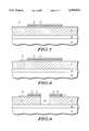
- FIG. 6includes a cross-sectional view of a portion of semiconductor substrate 10 with layers formed over it.
- Circuit element 11overlies the substrate 10.
- Circuit element 11could be one of a variety of items including a doped region within the substrate 10 or a conductive member, such as a gate electrode, a capacitor electrode, a contact or via plug, an interconnect, and the like, lying over the substrate 10.
- the circuit element 11is anything that is to be electrically connected to a high-permittivity metal-oxide capacitor to be formed.
- Substrate 10may be a semiconductor or insulating material. Insulating layer 12, lower electrode layer 13, metal-oxide dielectric layer 14, and upper electrode layer 15 are sequentially formed over the circuit element 11.
- the selection of materials for each of the layers above the circuit element 11depends on the device that is formed and other layers that a particular layer currently or subsequently contacts.
- a DRAMrequires a high-permittivity capacitor, but the metal-oxide dielectric layer 14 does not need to have ferroelectric properties.
- the metal-oxide layermay include tantalum pentoxide (Ta 2 O 5 ), a zirconate titanate (Zr x Ti y O z ), strontium titanate (SrTiO 3 ), barium strontium titanate (BST), lead zirconate titanate (PZT), lanthanum-doped PZT, or the like.
- the metal-oxide dielectric layer 14must have ferroelectric properties, and therefore, may include bismuth titanate (Bi 4 Ti 3 O 12 ), barium titanate (BaTiO 3 ), BST, PZT, lanthanum-doped PZT, or the like.
- Electrode layers 13 and 15depend in part on the material used for the dielectric layer 14. Lead reacts with or diffuses into many silicon-containing compounds. Electrode layers 13 and 15 should not include silicon-containing compounds or allow lead diffusion if 1) the metal-oxide dielectric layer includes lead and 2) the dielectric layer 14 is exposed to a temperature higher than about 500 degrees Celsius. If lead is present, the electrode layers 13 and 15 may include ruthenium, rhenium, iridium, osmium, any of the conductive metal oxides of the previous four elements, platinum, or the like. If the metal-oxide dielectric layer includes Ta 2 O 5 , the electrode layers 13 and 15 may include virtually any conductive material including doped silicon, metals, and metal-containing compounds.
- the insulating layer 12may include any conventional semiconductor insulating material, such as silicon dioxide, silicon nitride, or the like.
- the insulating layer 12includes a silicon dioxide layer and a thin top layer of titanium dioxide.
- the thin topmay not be needed or may be replaced by or used in conjunction with tantalum pentoxide, magnesium oxide, or the like, especially if the metal-oxide dielectric layer 14 includes lead and there is a possibility that the metal-oxide layer 14 may come in contact with the insulating layer 12 during high temperature processing.
- a thin titanium layermay be formed prior to forming the lower electrode layer 13 if the insulating layer does not include the thin titanium dioxide layer. The titanium layer would act as an adhesion layer between the insulating layer 12 and the lower electrode layer 13. Needless to say, the selection of materials for layers 12-15 depends on the type of device and the layers that will come in contact with any specific layer.
- the insulating layer 12is silicon dioxide and the lower electrode 13 is platinum.
- the metal-oxide dielectric layer 14is PZT and is deposited using a conventional method, such as sputter depositing, sol-gel coating, or chemical vapor deposition.
- the metal-oxide dielectric layer 14is annealed in an oxidizing ambient at a temperature between about 650-700 degrees Celsius.
- the annealing timeis typically between about 10-300 seconds for a rapid thermal processor and between about 5-30 minutes for a conventional furnace.
- the oxidizing ambientincludes oxygen and may include a gas diluent, such as nitrogen, helium, argon, and the like.
- a gas diluentsuch as nitrogen, helium, argon, and the like.
- the annealing temperaturemay be between about 500-800 degrees Celsius.
- the upper electrode 15is formed and made of platinum.
- the electrode layers 13 and 15 and metal-oxide layer 14are patterned using conventional methods.
- platinummay be wet etched or dry etched.
- Wet etchingmay be performed using an aqua regia solution or a modified aqua regia solution.
- the latteris an aqueous solution including hydrochloric (HCl) and nitric (HNO 3 ) acids and an etching solution at about 75 degrees Celsius.
- the etching solutionincludes 60-80 weight percent phosphoric acid H 3 PO 4 , 10-25 weight percent acetic acid (CH 3 COOH), 0.1-5 weight percent HNO 3 , and the remainder water.
- This etching solutionis commercially available from Olin Hunt Specialty Products, Inc. and is called M2STM.
- Dry etchingmay be performed using a method, such as ion milling.
- the metal-oxide dielectric layer 14may be patterned using wet or dry etching techniques.
- Wet etchingmay be performed with a solution including hydrofluoric acid, nitric acid, and hydrogen peroxide. The solution is maintained at about room temperature during the etch.
- Dry etchingmay be performed using plasma etching or ion milling.
- the etching chemistryshould include oxygen, fluorine-containing compounds, such as carbon tetrafluoride (CF 4 ) and the like, or chlorine-containing compounds, such as carbon tetrachloride (CCl 4 ), molecular chlorine (Cl 2 ), and the like.
- a first masking layer(not shown) is formed over the upper electrode layer 15.
- the upper electrode layer 15 and the metal-oxide dielectric layer 14are patterned using ion milling such that the edges of the two layers are substantially coincident with each other to form the patterned layers. After the ion milling step, the first masking layer is removed.
- the patterned metal-oxide and upper electrode layers 14 and 15are shown in FIG. 7. Some of the lower electrode layer 13 may be etched during the ion milling but is not shown in FIG. 7.
- a second masking layer(not shown) is formed over the electrode layers 13 and 15.
- the lower electrode layer 13is patterned by any of the wet or dry etching techniques used for platinum. After the lower electrode layer 13 is patterned, the second masking layer is removed.
- FIG. 8shows the device at this point in the process. The portion of the lower electrode layer 13 that extends beyond layers 14 and 15 allows a subsequently formed contact to reach the lower electrode layer 13.
- An opening 41is formed that extends through layers 12-15 to the circuit element 11 as shown in FIG. 9.
- a third masking layer(not shown) in formed over the upper electrode layer 15 where the opening 41 to the circuit element 11 is to be formed.
- the opening 41may be formed by ion milling through the layers 13-15 and then plasma etching the insulating layer 12.
- the ion millingallows layers 13-15 to be patterned while keeping the edges of the layers adjacent to the opening substantially coincident with one another.
- the ion millingmay extend partially into the insulating layer 12.
- the plasma etch of the insulating layerusually provides an etch that is more selective with respect to circuit element 11 than can be achieved with ion milling.
- the plasma etchingdoes not usually erode the third masking layer as fast as ion milling.
- the opening 41may be formed completely by ion milling if the third masking layer is thick enough to account for the ion milling of layers 12-15.
- Other conventional etching methodsmay be used to form the opening 41, such as wet etching or other dry etching techniques. After opening 41 is formed, the third masking layer is removed.
- Insulating spacers 51 and 52are formed along exposed edges of layers 12-15 as shown in FIG. 10.
- the selection of the material for the insulating spacer 51depends on the material used for the metal-oxide dielectric layer 14 and temperature cycles to which the insulating spacer 51 is subsequently subjected.
- the metal oxide layer 14includes lead (from the PZT) that may react with silicon-containing insulating materials if the device is exposed to a temperature higher than about 500 degrees Celsius. Therefore, the insulating spacer 51 may include titanium dioxide (TiO 2 ), tantalum pentoxide (Ta 2 O 5 ), magnesium oxide (MgO), or the like.
- One method of forming the spacers 51 and 52may be to: 1) deposit titanium and thermally oxidize it to form titanium dioxide, and 2) anisotropically etching the titanium dioxide using a fluorine-containing plasma.
- the spacers 51 and 52may be formed by depositing TiO 2 or Ta 2 O 5 by reactive sputtering or chemical vapor deposition followed by an anisotropic etch. If the metal-oxide dielectric layer does not contain lead or is not exposed to a temperature higher than about 500 degrees Celsius, silicon-containing materials may be used in spacers 51 and 52. Needless to say, many different materials and deposition and etching methods may be used.
- the deposition of the material used for the insulating spacers 51 and 52should be conformal, although this is not a requirement.
- the insulating material for the insulating spacers 51 and 52is deposited to a thickness between about 100-3000 angstroms thick. At least some of the insulating material should be deposited along the exposed side edges of layers 13 and 14.
- the etching to form the spacers 51 and 52should be primarily anisotropic. The etching may include some isotropic etching, but once again, at least some of the insulating spacer 51 must lie adjacent to the layers 13 and 14. When the insulating spacer 51 formation is completed, the spacers 51 must be thick enough to prevent an electrical connection between a subsequently formed conductive member that is formed within the opening 41 and either the lower electrode layer 13 or the metal-oxide dielectric layer 14.
- a conductive member 61is formed that electrically connects the circuit element 11 to the upper electrode layer 15 as shown in FIG. 11.
- the conductive member 61may include silicon, a metal, or a metal-containing compound.
- a conductive layeris deposited by a conventional method, such as chemical vapor deposition, sputter deposition, and the like.
- a fourth masking layer(not shown) is formed over the conductive layer where the conductive member 61 is to be formed. The exposed portions of the conductive layer are etched leaving conductive member 61. The fourth masking layer is removed after the conductive member 61 has been formed.
- Polysilicon, tungsten, or titanium nitridemay be conformally formed and patterned to form the conductive member 61.
- any conductive material that can be deposited and patterned while leaving at least some conductive material along the side of the insulating spacer 51may be used.
- the conductive membermay include more than one part.
- a conductive plug including tungsten, polysilicon, or the likemay be formed that partially or completely fills the opening 41.
- a local interconnectmay be formed that contacts the conductive plug and the upper electrode layer 15. In this case, the combination of the conductive plug and the local interconnect forms the conductive member 61.
- FIG. 12A substantially completed device is shown in FIG. 12.
- a second insulating layer 71is formed over the substrate 10 including the conductive member 61.
- An opening and a conductive plug 72are sequentially formed within the second insulating layer 71 that makes electrical connection to the lower electrode layer 13.
- An interconnect 73 and a passivation layer 74are formed. Other layers and electrical connections (not shown) may be formed if needed.
- the capacitor and connection to the circuit elementdo not have the prior art strap that occupies valuable substrate area.
- the conductive member 61is formed after most of the high temperature processing is completed.
- the conductive member between a circuit element and the lower electrodeis formed prior to annealing its metal-oxide dielectric layer.
- the conductive member of the prior art stacked capacitormay have adverse interactions, such as reactions, deformation, melting, diffusion, and the like, with adjacent layers or the oxidizing ambient during the anneal.
- the conductive member 61is formed after the annealing step of the metal-oxide dielectric layer 14.
- the conductive member 61should not have any adverse interactions with adjacent layers or the oxidizing ambient during the anneal. If the conductive member 61 is a conductive metal oxide or metal that can form a conductive metal oxide, the device may be subjected to an oxidizing ambient after conductive member 61 is formed. Another benefit is the simplicity of formation of the device. Process integration issues are not expected to be difficult.
- the patterning of layers 13-15 prior to forming any portion of the opening 41may take many forms. Each of layers 13-15 may be patterned separately, layer 14 may be patterned with layer 13 or layer 15, or the three layers may be patterned during one step. Also, the patterning of the layers 13-15 outside of the opening 41 may be performed after the conductive member 61 is formed.
- the insulating layer that forms the insulating spacers 51 and 52may be formed using many different methods. That insulating layer may be chemically deposited or sputter deposited (reactively or otherwise).
- the insulating layer for the insulating spacers 51 and 52may be formed by depositing a material and subsequently oxidizing it to form an insulating layer.
- the oxidation to form the insulating spacersmay be performed after the spacers are formed.
- circuit element 11must be able to withstand a thermal oxidation cycle without forming an insulating layer between the circuit element 11 and the subsequently formed conductive member 61. If the spacer material is oxidized to form spacers 51 and 52 after the circuit element 11 is exposed, circuit element 11 should not form an insulator.
- specific thicknesseshave been given, other thicknesses may be used without departing from the spirit or scope of the present invention. The options listed herein are meant to be illustrative and not limiting.
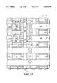
- FIGS. 13 and 14include an NVRAM cell 100 having a transistor 103 and a ferroelectric capacitor 105.
- FIG. 13is a plan view of the NVRAM cell 100
- FIG. 14is a cross-sectional view of the NVRAM cell 100.
- Interconnect 101acts as a bit line and has a length that generally extends between the left-hand side and the right-hand side of FIG. 13. A portion of interconnect 101 is not shown in FIG. 13 to more clearly show the underlying elements of the NVRAM cell 100.
- a conductive plug 1011electrically connects the interconnect 101 to a first doped region 109 that acts as a source/drain region of transistor 103.
- Transistor 103further includes a conductive member 102 that acts as a word line for the NVRAM cell 100 and a second doped region (not shown in FIG. 13) that acts as the other source/drain region for transistor 103 and underlies the ferroelectric capacitor 105.
- the ferroelectric capacitor 105includes a lower electrode layer 106 that acts as the drive line for the NVRAM cell 100, a metal-oxide dielectric layer (not shown in FIG. 13) that acts as the ferroelectric dielectric, and an upper electrode layer 107.
- Conductive member 117electrically connects the upper electrode layer 107 to the second doped region of transistor 103 via opening 104.
- a conductive member 117is not electrically connected to either the lower electrode layer 106 or the metal-oxide dielectric layer of the ferroelectric capacitor 105.
- FIG. 13includes field isolation region 108 that defines the active area of the transistor 103.
- FIG. 14includes a cross-sectional illustration of a portion of the NVRAM cell 100 as indicated in FIG. 13.
- the cross-sectional descriptiongenerally follows the order in which the elements of the cell are formed.
- the NVRAM cell 100is formed on a region 110.
- the region 110may be a p-well region in an n-type substrate (not shown) or a p-type region that has a higher doping concentration that a p-type substrate (not shown) in which the p-type region lies.
- Field isolation region 108is formed using a conventional field isolation process sequence, such as a local oxidation of silicon (LOCOS) process.
- LOClocal oxidation of silicon
- a gate dielectric layer 113 and a conductive member 102are formed.
- the gate dielectric layermay be formed by thermal oxidation or by chemical vapor deposition.
- a conductive layeris formed by depositing a layer that is conductive or can be made conductive by doping it, such as polysilicon, amorphous silicon and the like.
- the gate dielectric and conductive layersare patterned to form the gate structure shown in FIG. 14 including gate dielectric layer 113 and conductive member 102.
- the doped regions 109 and 112are formed within the semiconductor substrate 110 by 1) lightly doping the exposed portions of the substrate with an n-type dopant, 2) forming sidewall spacers 1031 adjacent to the gate structure, and 3) heavily doping the exposed portions of the substrate with an n-type dopant.
- transistor 103has been formed and includes the doped regions 109 and 112, the gate dielectric layer 113, the conductive member 102, and a channel region.
- the channel regionis the portion of the substrate that lies between the doped regions 109 and 112 and immediately beneath the gate dielectric layer 113.
- the next portion of the process sequenceis used to form the ferroelectric capacitor 105.
- a first insulating layer 114is formed over the substrate 110 and the transistor 103.
- Lower electrode layer 106, metal-oxide layer 115, and upper electrode layer 107are formed and patterned using an embodiment described in conjunction with forming and patterning layers 13-15 that was described in the section entitled "Metal-Oxide Capacitor" relating to a ferroelectric capacitor.
- the ferroelectric capacitor 105requires that the metal-oxide layer 115 act as a ferroelectric dielectric. Therefore, the metal-oxide layer 115 may include BST, PZT, lanthanum-doped PZT, or the like.
- the lower electrode layer 106acts as the drive line for the NVRAM cell 100.
- the lower electrode layer 106must be patterned separately from the upper electrode layer 107.
- the metal-oxide layer 115may be patterned during the same patterning step as either electrode layer 106 or 107 or may be patterned separately. Otherwise, many of the material options for the electrodes 106 and 107 and processing options available to form the capacitor described in an earlier embodiment may be used in forming the ferroelectric capacitor 105.
- An anneal with an oxidizing ambient similar to one previously describedis performed anytime after the metal-oxide layer 115 is deposited. Also, other anneals may be provided at various points in the process sequence prior to forming the conductive member 117, although this is not required.
- the next portion of the process sequenceelectrically connects the upper electrode layer 107 of the ferroelectric capacitor 105 with the second doped region 112 of the transistor 103.
- An opening 104is formed through layers 107, 115, 106, and 114 to the second doped region 112.
- Insulating spacer 116is formed within opening 104, and insulating spacers 1051 are formed adjacent to layers 107, 115, and 106 in locations outside the opening 104. If the insulating spacers 116 and 1051 are exposed to a temperature higher about 500 degrees Celsius, the insulating spacers should not include silicon-containing compounds.
- the insulating spacers 116 and 1051may include titanium dioxide, tantalum pentoxide, magnesium oxide, or the like.
- the insulating spacers 116 and 1051may include silicon-containing compounds, such as silicon dioxide, silicon nitride, and the like.
- a conductive member 117is formed.
- the materials and processing options discussed with respect to forming opening 41, insulating spacers 51 and 52, and conductive member 61 in the section entitled "Metal-Oxide Capacitor"apply to corresponding elements of opening 104, insulating spacers 116 and 1051, and conductive member 117 to the extent those options are not contrary to concerns discussed within this paragraph.
- a second insulating layer 118is formed over the conductive member 117 and the first insulating layer 114.
- a contact openingis formed that extends through the first and second insulating layers 114 and 118 to the first doped region 109.
- Conductive plug 1011fills the contact opening.
- Interconnect 101is formed over the conductive plug 1011.
- a passivation layer 119is formed over the device including the interconnect 101 to form a substantially completed device. Interconnect 101 extends across the entire length of the NVRAM cell 100 and is illustrated as such in FIG. 14. Other layers and electrical connections (not shown) may be formed if needed.
- the NVRAM cell 100has many benefits compared to the prior art NVRAM cell 90.
- the interconnects 91 and 94cause the cell 90 to be quite large. Minimum spacing requirements are needed at both the contact opening and interconnect levels to assure a reliable process.
- the cell sizeis not typically limited by the capacitor area, so that a large capacitor area may be used even if the large capacitor area is not required. Therefore, the cell 90 may occupy an area of about 840 square microns and have a capacitor area of about 200 square microns for a four micron minimum feature size.
- NVRAM cell 100has a cell area that is determined more by the capacitor area as opposed to the contact or interconnect spacing concerns.
- NVRAM cell 100occupies an area of about 320 square microns and has a capacitor area of about 110 square microns. Although the NVRAM cell 100 is about three times smaller than the prior art cell 90, an NVRAM cell of the present invention should be at least twice as small as a prior art strapped cell when using similar design rules.
- the present inventionalso has advantages over a stacked capacitor NVRAM cell.
- a conductive memberwhich electrically connects a source/drain region of the transistor to the lower electrode layer of the ferroelectric capacitor in a stacked NVRAM cell, is formed prior to the annealing of the metal-oxide dielectric layer 115 to give it ferroelectric properties.
- the annealmay cause the conductive member to oxidize or have adverse interactions with layers adjacent to that conductive member.
- the NVRAM cell 100 of the present inventiondoes not form the conductive member between the second doped region 112 of the transistor 103 and the upper electrode layer 107 of the ferroelectric capacitor 105 until after all of the anneals for the metal-oxide layer 115 have been performed. Therefore, no adverse interactions between the conductive member 117 and other portions of the NVRAM cell 100 should occur.
- the NVRAM cell 100is typically one of a plurality of cells within a memory array.
- the NVRAM cell 100 within the arrayis typically surrounded by NVRAM cells on all four sides.
- the cells on the each sidehas a plan view that is a mirror image of the NVRAM cell 100 as shown in FIG. 13.
- Interconnect 101acts as the bit line for NVRAM cell 100 as well as those cells to the left and right of that cell with respect to FIG. 13.
- FIG. 15includes a plan view of a portion of an NVRAM memory array 1200 including an NVRAM cell 120 that is shown by dashed lines.
- the NVRAM cell 120includes two transistors 121 and 123 and two ferroelectric capacitors 122 and 124 and has a circuit diagram similar to the one shown in FIG. 3.
- Interconnects 1210 and 1230act as the complementary bit lines BL and BL, respectively. Although interconnects 1210 and 1230 extend completely across the length of the NVRAM cell 120, portions of interconnects 1210 and 1230 are not shown in FIG. 15, so that underlying elements can be more clearly seen.
- Interconnect 1210is electrically connected to a first doped region 1211 that acts as a source/drain region of transistor 121.
- Transistor 121also includes a second doped region 1213 that acts as the other source/drain region for the transistor.
- Conductive member 1212acts as the gate electrode for transistor 121.
- Interconnect 1230is electrically connected to a third doped region 1231 that acts as a source/drain of transistor 123.
- Transistor 123also includes a fourth doped region 1233 that acts as the other source/drain region for the transistor.
- Conductive member 1212acts as the gate electrode for transistor 123.
- Conductive member 1212also acts as the word line for the NVRAM cell 120. Active regions for transistors 121 and 123 are defined by the field isolation region 135.
- Capacitors 122 and 124include a lower electrode layer 131 and upper electrodes 1340 and 1341.
- the lower electrode layer 131acts as the drive line and underlies substantially all of the upper electrodes 1340 and 1341.
- Opening 1342extends through the ferroelectric capacitor 122 to the second doped region 1213, and opening 1344 extends through the ferroelectric capacitor 124 to the fourth doped region 1233.
- Conductive member 1346extends through the opening 1342 and electrically connects the second doped region 1213 to the upper electrode 1340 for the ferroelectric capacitor 122.
- Conductive member 1348extends through the opening 1344 and electrically connects the fourth doped region 1233 to the upper electrode 1341 for the ferroelectric capacitor 124.
- FIG. 16includes an NVRAM cell 140 that has a circuit diagram similar to the one shown in FIG. 4.
- FIG. 16includes a cross-sectional view of a portion of the NVRAM cell 140 parallel with the length of one of the bit lines.
- An n-well 1501 and a p-well 1502lie within a semiconductor substrate 1500.
- Field isolation region 1503separates the transistors 141 and 142 from one another.
- Transistor 141includes a gate dielectric layer 1511, conductive member 1522 that acts as a gate electrode, and first and second doped regions 1524 and 1525 that act as the source/drain regions for the transistor.
- Transistor 142includes a gate dielectric layer 1511, conductive member 1528 that acts as a gate electrode, and third and fourth doped regions 1526 and 1527 that act as the source/drain regions for the transistor.
- Gate electrode 1522acts as one word line (WL) and gate electrode 1528 acts as the complementary word line (WL).
- Adjacent to the gate electrodesare spacers 1523 that are formed with the process sequence used in forming the doped regions 1524-1527.
- First and second doped regions 1524 and 1525are P + regions, and third and fourth doped regions 1526 and 1527 are N + regions.
- a first insulating layer 1531is formed over the transistors 141 and 142.
- the ferroelectric capacitor 143is formed over the first insulating layer 1531.
- the ferroelectric capacitor 143includes a lower electrode layer 1541 that acts as the drive line for the NVRAM cell 140, a metal-oxide dielectric layer 1542 that acts as the ferroelectric dielectric, and an upper electrode layer 1543. Openings 1544 extend through the upper electrode layer 1543, the metal-oxide dielectric layer 1542, the lower electrode layer 1541, and the first insulating layer 1531 to the second and third doped regions 1525 and 1526.
- Insulating spacers 1545are formed within openings 1544, and insulating spacers 1547 are formed adjacent to layers 1541-1543 in locations outside the openings 1544.
- a conductive member 1546lies over the upper electrode layer 1543 and adjacent the insulating spacers 1545 within the openings 1544.
- the conductive member 1546electrically connects the second and third doped regions 1525 and 1526 and the upper electrode layer 1543 to one another.
- a second insulating layer 1551is formed over the conductive member 1546 and the first insulating layer 1531. Contact openings are formed to expose portions of the first and fourth doped regions 1524 and 1527.
- An interconnect 1552is formed over the second insulating layer 1551 and within the contact openings. Interconnect 1552 acts as a bit line (BL) and is electrically connected to first and fourth doped regions 1524 and 1527 of transistors 141 and 142, respectively.
- a passivation layer 1553is formed over the interconnect 1552 to form a substantially finished device. Other layers and electrical connections (not shown) may be formed, if needed.
- the NVRAM cell 140includes another p-channel transistor, an n-channel transistor, a ferroelectric capacitor, and a complementary bit line (BL) but are not shown in FIG. 16. These other components would be oriented similar to those shown in FIG. 16 and would lie generally parallel with the length of the interconnect 1552 and either just in front of or just behind the components shown in FIG. 16. With this orientation, the length of the bit lines are generally parallel with one another, and the length of the drive line is generally perpendicular to the bit lines.
- the NVRAM cell 140is not limited the embodiment shown or described. Many of the options available to the other NVRAM cells previously described are also available to the NVRAM cell 140.
- FIG. 5includes a circuit diagram for a DRAM cell.
- a cross-sectional view of one embodiment of the DRAM cellwould visually appear to be nearly identical to NVRAM cell 100 of FIG. 14. It should be kept in mind that the capacitor of the DRAM cell should not have ferroelectric properties over the normal operating temperature range of the DRAM cell.
- the ferroelectric capacitor 105is replaced with a high-permittivity capacitor, and the metal-oxide layer is not processed to achieve ferroelectric properties over the normal operating temperature range of the DRAM cell.
- the metal-oxide dielectric layermay include any of the materials that are listed with those previously described in the high-permittivity capacitor section. Although an anneal may need to be performed to form a high-permittivity metal-oxide dielectric layer, the anneal would not be performed to give the metal-oxide dielectric layer the ferroelectric properties.
- the choice of material for the insulating spacer 116depends on the material used for the metal-oxide dielectric layer and the thermal cycles to which the insulating spacer will be exposed. If the metal-oxide dielectric layer 115 includes lead and the insulating spacer 116 is exposed to a temperature higher than about 500 degrees Celsius, the insulating spacer 116 should be a non-silicon-containing material, such as TiO 2 , Ta 2 O 5 , MgO, and the like. Otherwise, the insulating spacer may include a silicon-containing material, such as silicon dioxide, silicon nitride, and the like.
Landscapes
- Semiconductor Memories (AREA)
- Semiconductor Integrated Circuits (AREA)
- Non-Volatile Memory (AREA)
Abstract
Description
Claims (11)
Priority Applications (10)
| Application Number | Priority Date | Filing Date | Title |
|---|---|---|---|
| US08/100,793US5439840A (en) | 1993-08-02 | 1993-08-02 | Method of forming a nonvolatile random access memory capacitor cell having a metal-oxide dielectric |
| TW083105275ATW293181B (en) | 1993-08-02 | 1994-06-10 | |
| EP94110844AEP0637845B1 (en) | 1993-08-02 | 1994-07-12 | Capacitor having a metal-oxide dielectric |
| DE69428487TDE69428487T2 (en) | 1993-08-02 | 1994-07-12 | Metal oxide dielectric capacitor |
| SG1996003665ASG48908A1 (en) | 1993-08-02 | 1994-07-12 | Capacitor having a metal-oxide dielectric |
| CN94114807ACN1051403C (en) | 1993-08-02 | 1994-07-25 | Capacitor having a metal-oxide dielectric |
| KR1019940019072AKR100372969B1 (en) | 1993-08-02 | 1994-08-02 | Capacitor having a Metal-Oxide Dielectric |
| JP19893394AJP4008047B2 (en) | 1993-08-02 | 1994-08-02 | Semiconductor device |
| US08/430,680US5583068A (en) | 1993-08-02 | 1995-04-28 | Process for forming a capacitor having a metal-oxide dielectric |
| US08/664,327US5696394A (en) | 1993-08-02 | 1996-06-14 | Capacitor having a metal-oxide dielectric |
Applications Claiming Priority (1)
| Application Number | Priority Date | Filing Date | Title |
|---|---|---|---|
| US08/100,793US5439840A (en) | 1993-08-02 | 1993-08-02 | Method of forming a nonvolatile random access memory capacitor cell having a metal-oxide dielectric |
Related Child Applications (2)
| Application Number | Title | Priority Date | Filing Date |
|---|---|---|---|
| US39730295ADivision | 1993-08-02 | 1995-03-01 | |
| US08/430,680DivisionUS5583068A (en) | 1993-08-02 | 1995-04-28 | Process for forming a capacitor having a metal-oxide dielectric |
Publications (1)
| Publication Number | Publication Date |
|---|---|
| US5439840Atrue US5439840A (en) | 1995-08-08 |
Family
ID=22281565
Family Applications (3)
| Application Number | Title | Priority Date | Filing Date |
|---|---|---|---|
| US08/100,793Expired - Fee RelatedUS5439840A (en) | 1993-08-02 | 1993-08-02 | Method of forming a nonvolatile random access memory capacitor cell having a metal-oxide dielectric |
| US08/430,680Expired - LifetimeUS5583068A (en) | 1993-08-02 | 1995-04-28 | Process for forming a capacitor having a metal-oxide dielectric |
| US08/664,327Expired - LifetimeUS5696394A (en) | 1993-08-02 | 1996-06-14 | Capacitor having a metal-oxide dielectric |
Family Applications After (2)
| Application Number | Title | Priority Date | Filing Date |
|---|---|---|---|
| US08/430,680Expired - LifetimeUS5583068A (en) | 1993-08-02 | 1995-04-28 | Process for forming a capacitor having a metal-oxide dielectric |
| US08/664,327Expired - LifetimeUS5696394A (en) | 1993-08-02 | 1996-06-14 | Capacitor having a metal-oxide dielectric |
Country Status (8)
| Country | Link |
|---|---|
| US (3) | US5439840A (en) |
| EP (1) | EP0637845B1 (en) |
| JP (1) | JP4008047B2 (en) |
| KR (1) | KR100372969B1 (en) |
| CN (1) | CN1051403C (en) |
| DE (1) | DE69428487T2 (en) |
| SG (1) | SG48908A1 (en) |
| TW (1) | TW293181B (en) |
Cited By (37)
| Publication number | Priority date | Publication date | Assignee | Title |
|---|---|---|---|---|
| US5500386A (en)* | 1993-12-28 | 1996-03-19 | Matsushita Electronics Corporation | Manufacturing method of semiconductor devices |
| US5527729A (en)* | 1994-03-30 | 1996-06-18 | Matsushita Electronics Corporation | Method of manufacturing a capacitor having metal electrodes |
| US5567636A (en)* | 1995-02-27 | 1996-10-22 | Motorola Inc. | Process for forming a nonvolatile random access memory array |
| US5622882A (en)* | 1994-12-30 | 1997-04-22 | Lsi Logic Corporation | Method of making a CMOS dynamic random-access memory (DRAM) |
| US5654223A (en)* | 1995-06-27 | 1997-08-05 | Lg Semicon Co., Ltd. | Method for fabricating semiconductor memory element |
| US5661063A (en)* | 1994-05-13 | 1997-08-26 | Samsung Electronics Co., Ltd. | Semiconductor memory device provided with capacitors formed above and below a cell transistor and method for manufacturing the same |
| US5696394A (en)* | 1993-08-02 | 1997-12-09 | Motorola, Inc. | Capacitor having a metal-oxide dielectric |
| US5712813A (en)* | 1996-10-17 | 1998-01-27 | Zhang; Guobiao | Multi-level storage capacitor structure with improved memory density |
| DE19640211A1 (en)* | 1996-09-30 | 1998-04-02 | Siemens Ag | Method for manufacturing barrier-free semiconductor memory devices |
| DE19640413A1 (en)* | 1996-09-30 | 1998-04-02 | Siemens Ag | Method for manufacturing barrier-free semiconductor memory devices |
| US5750419A (en)* | 1997-02-24 | 1998-05-12 | Motorola, Inc. | Process for forming a semiconductor device having a ferroelectric capacitor |
| US5789323A (en)* | 1995-04-25 | 1998-08-04 | Ramtron International Corporation | Fabrication of metal-ferroelectric-metal capacitors with a two step patterning sequence |
| US5796133A (en)* | 1993-01-27 | 1998-08-18 | Samsung Electronics Co., Ltd. | Semiconductor device capacitor having lower electrodes separated by low dielectric spacer material |
| US5838530A (en)* | 1996-07-22 | 1998-11-17 | Zhang; Guobiao | Applications of protective ceramics |
| US5851868A (en)* | 1995-09-19 | 1998-12-22 | Samsung Electronics Co., Ltd. | Methods of forming integrated decoupling capacitors |
| US5923056A (en)* | 1996-10-10 | 1999-07-13 | Lucent Technologies Inc. | Electronic components with doped metal oxide dielectric materials and a process for making electronic components with doped metal oxide dielectric materials |
| US5926359A (en)* | 1996-04-01 | 1999-07-20 | International Business Machines Corporation | Metal-insulator-metal capacitor |
| US5960253A (en)* | 1997-02-18 | 1999-09-28 | Mitsubishi Denki Kabushiki Kaisha | Method of manufacturing semiconductor memory device capable of readily repairing defective portion resulting from mask defect |
| US6004839A (en)* | 1996-01-17 | 1999-12-21 | Nec Corporation | Semiconductor device with conductive plugs |
| WO2000016400A1 (en)* | 1998-09-16 | 2000-03-23 | Guobiao Zhang | Applications of protective ceramics |
| US6054340A (en)* | 1997-06-06 | 2000-04-25 | Motorola, Inc. | Method for forming a cavity capable of accessing deep fuse structures and device containing the same |
| US6071785A (en)* | 1995-09-28 | 2000-06-06 | Nec Corporation | Low resistance ground wiring in a semiconductor device |
| US6111742A (en)* | 1997-09-22 | 2000-08-29 | Stmicroelectronics S.A. | Implementation of an intermetallic capacitor |
| US6174766B1 (en)* | 1997-06-18 | 2001-01-16 | Nec Corporation | Semiconductor device and method of manufacturing the semiconductor device |
| US6174822B1 (en)* | 1997-06-24 | 2001-01-16 | Matsushita Electronics Corporation | Semiconductor device and method for fabricating the same |
| US6344413B1 (en) | 1997-12-22 | 2002-02-05 | Motorola Inc. | Method for forming a semiconductor device |
| US6429089B1 (en)* | 1997-08-21 | 2002-08-06 | Nec Corporation | Semiconductor device and method of fabricating the same |
| US6432793B1 (en) | 1997-12-12 | 2002-08-13 | Micron Technology, Inc. | Oxidative conditioning method for metal oxide layer and applications thereof |
| KR100359551B1 (en)* | 1999-02-17 | 2002-11-07 | 인터내셔널 비지네스 머신즈 코포레이션 | Triple polysilicon embedded nvram cell and method thereof |
| US20030089943A1 (en)* | 1999-01-04 | 2003-05-15 | International Business Machines Corporation | BEOL decoupling capacitor |
| US20040228066A1 (en)* | 2003-05-16 | 2004-11-18 | Nec Electronics Corporation | Capacitor cell, semiconductor device and process for manufacturing the same |
| US20050265067A1 (en)* | 1997-12-12 | 2005-12-01 | Hyundai Electronics Industries Co., Ltd. | Ferroelectric memory device and method of making the same |
| US20060214204A1 (en)* | 2005-03-23 | 2006-09-28 | Dong-Chul Yoo | Ferroelectric structures and devices including upper/lower electrodes of different metals and methods of forming the same |
| US20100277986A1 (en)* | 2009-04-29 | 2010-11-04 | Taiwan Semiconductor Manufacturing Company, Ltd. | Non-volatile field programmable gate array |
| US20110108929A1 (en)* | 2002-08-26 | 2011-05-12 | Round Rock Research, Llc | Enhanced atomic layer deposition |
| US20210342659A1 (en)* | 2020-05-01 | 2021-11-04 | X-Celeprint Limited | Hybrid documents with electronic indicia |
| US12414471B2 (en) | 2020-05-01 | 2025-09-09 | X-Celeprint Limited | Piezoelectric power components |
Families Citing this family (52)
| Publication number | Priority date | Publication date | Assignee | Title |
|---|---|---|---|---|
| JPH05243487A (en)* | 1992-03-02 | 1993-09-21 | Nec Corp | Integrated circuit |
| TW403972B (en) | 1993-01-18 | 2000-09-01 | Semiconductor Energy Lab | Method of fabricating mis semiconductor device |
| EP0738014B1 (en)* | 1993-08-05 | 2003-10-15 | Matsushita Electric Industrial Co., Ltd. | Manufacturing method of semiconductor device having high dielectric constant capacitor |
| JP3666893B2 (en)* | 1993-11-19 | 2005-06-29 | 株式会社日立製作所 | Semiconductor memory device |
| JP2982855B2 (en)* | 1994-09-20 | 1999-11-29 | 日本電気株式会社 | Semiconductor device and manufacturing method thereof |
| KR0168346B1 (en)* | 1994-12-29 | 1998-12-15 | 김광호 | Capacitor using high deelectric material and its fabrication method |
| KR0161785B1 (en)* | 1995-04-29 | 1998-12-01 | 주승기 | Method of manufacturing ferroelectric thin film device |
| JP3480866B2 (en)* | 1995-05-18 | 2003-12-22 | 松下電器産業株式会社 | Semiconductor device and method of manufacturing the same |
| KR0147655B1 (en)* | 1995-07-13 | 1998-08-01 | 김광호 | Manufacturing method for capacitor of semiconductor device |
| US5914851A (en)* | 1995-12-22 | 1999-06-22 | International Business Machines Corporation | Isolated sidewall capacitor |
| SG54456A1 (en)* | 1996-01-12 | 1998-11-16 | Hitachi Ltd | Semconductor integrated circuit device and method for manufacturing the same |
| US6660610B2 (en)* | 1996-07-08 | 2003-12-09 | Micron Technology, Inc. | Devices having improved capacitance and methods of their fabrication |
| JP3512959B2 (en)* | 1996-11-14 | 2004-03-31 | 株式会社東芝 | Semiconductor device and manufacturing method thereof |
| TW378345B (en)* | 1997-01-22 | 2000-01-01 | Hitachi Ltd | Resin package type semiconductor device and manufacturing method thereof |
| KR100227843B1 (en)* | 1997-01-22 | 1999-11-01 | 윤종용 | Contact wiring method of semiconductor device and capacitor manufacturing method using same |
| KR100295568B1 (en)* | 1997-02-03 | 2001-09-07 | 니시무로 타이죠 | Semiconductor device and method of manufacturing the same |
| US5893731A (en)* | 1997-05-23 | 1999-04-13 | Industrial Technology Research Institute | Method for fabricating low cost integrated resistor capacitor combinations |
| US6193832B1 (en) | 1997-07-25 | 2001-02-27 | International Business Machines Corporation | Method of making dielectric catalyst structures |
| US6130182A (en)* | 1997-07-25 | 2000-10-10 | International Business Machines Corporation | Dielectric catalyst structures |
| US6197267B1 (en) | 1997-07-25 | 2001-03-06 | International Business Machines Corporation | Catalytic reactor |
| US6320214B1 (en)* | 1997-12-24 | 2001-11-20 | Matsushita Electric Industrial Co., Ltd. | Semiconductor device having a ferroelectric TFT and a dummy element |
| US6207465B1 (en)* | 1998-04-17 | 2001-03-27 | Symetrix Corporation | Method of fabricating ferroelectric integrated circuit using dry and wet etching |
| US6348411B1 (en)* | 1998-09-03 | 2002-02-19 | Micron Technology, Inc. | Method of making a contact structure |
| US6249014B1 (en)* | 1998-10-01 | 2001-06-19 | Ramtron International Corporation | Hydrogen barrier encapsulation techniques for the control of hydrogen induced degradation of ferroelectric capacitors in conjunction with multilevel metal processing for non-volatile integrated circuit memory devices |
| JP3517876B2 (en)* | 1998-10-14 | 2004-04-12 | セイコーエプソン株式会社 | Ferroelectric thin film element manufacturing method, ink jet recording head, and ink jet printer |
| US6174735B1 (en)* | 1998-10-23 | 2001-01-16 | Ramtron International Corporation | Method of manufacturing ferroelectric memory device useful for preventing hydrogen line degradation |
| US6038163A (en)* | 1998-11-09 | 2000-03-14 | Lucent Technologies Inc. | Capacitor loaded memory cell |
| JP2000183295A (en)* | 1998-12-16 | 2000-06-30 | Matsushita Electronics Industry Corp | Semiconductor memory device and method of manufacturing the same |
| KR100293713B1 (en) | 1998-12-22 | 2001-07-12 | 박종섭 | Method of manufacturing capacitor of memory element |
| US6252275B1 (en) | 1999-01-07 | 2001-06-26 | International Business Machines Corporation | Silicon-on-insulator non-volatile random access memory device |
| US6255157B1 (en) | 1999-01-27 | 2001-07-03 | International Business Machines Corporation | Method for forming a ferroelectric capacitor under the bit line |
| US6316797B1 (en)* | 1999-02-19 | 2001-11-13 | Advanced Technology Materials, Inc. | Scalable lead zirconium titanate(PZT) thin film material and deposition method, and ferroelectric memory device structures comprising such thin film material |
| US6218256B1 (en) | 1999-04-13 | 2001-04-17 | Micron Technology, Inc. | Electrode and capacitor structure for a semiconductor device and associated methods of manufacture |
| US6124199A (en) | 1999-04-28 | 2000-09-26 | International Business Machines Corporation | Method for simultaneously forming a storage-capacitor electrode and interconnect |
| US6284551B1 (en) | 1999-06-14 | 2001-09-04 | Hyundai Electronics Industries Co., Ltd. | Capacitor and method for fabricating the same |
| US6509592B2 (en)* | 1999-12-09 | 2003-01-21 | Matsushita Electric Industrial Co., Ltd. | Ferroelectric memory |
| US6452251B1 (en) | 2000-03-31 | 2002-09-17 | International Business Machines Corporation | Damascene metal capacitor |
| US6717193B2 (en) | 2001-10-09 | 2004-04-06 | Koninklijke Philips Electronics N.V. | Metal-insulator-metal (MIM) capacitor structure and methods of fabricating same |
| US6971165B1 (en)* | 2002-04-17 | 2005-12-06 | Borealis Technical Limited | Method for fabrication of separators for electrode pairs in diodes |
| US6916722B2 (en)* | 2002-12-02 | 2005-07-12 | Taiwan Semiconductor Manufacturing Co., Ltd. | Method to fabricate high reliable metal capacitor within copper back-end process |
| US20040166678A1 (en)* | 2003-02-24 | 2004-08-26 | Hall Lindsey H. | Wet clean method for PZT capacitors |
| US7101785B2 (en)* | 2003-07-22 | 2006-09-05 | Infineon Technologies Ag | Formation of a contact in a device, and the device including the contact |
| WO2005074032A1 (en)* | 2004-01-28 | 2005-08-11 | Fujitsu Limited | Semiconductor device and its manufacturing method |
| JP4948762B2 (en)* | 2004-12-27 | 2012-06-06 | 富士通株式会社 | Semiconductor device |
| JP4189378B2 (en)* | 2004-12-27 | 2008-12-03 | 株式会社東芝 | Ferroelectric memory |
| EP1677371A1 (en) | 2004-12-30 | 2006-07-05 | STMicroelectronics S.r.l. | Dual resistance heater for phase change devices and manufacturing method thereof |
| KR100717813B1 (en)* | 2005-06-30 | 2007-05-11 | 주식회사 하이닉스반도체 | Capacitors with nanomixed dielectric films and methods for manufacturing the same |
| US7226831B1 (en)* | 2005-12-27 | 2007-06-05 | Intel Corporation | Device with scavenging spacer layer |
| US9092582B2 (en) | 2010-07-09 | 2015-07-28 | Cypress Semiconductor Corporation | Low power, low pin count interface for an RFID transponder |
| US9846664B2 (en) | 2010-07-09 | 2017-12-19 | Cypress Semiconductor Corporation | RFID interface and interrupt |
| US8723654B2 (en) | 2010-07-09 | 2014-05-13 | Cypress Semiconductor Corporation | Interrupt generation and acknowledgment for RFID |
| JP6259023B2 (en) | 2015-07-20 | 2018-01-10 | ウルトラテック インク | Masking method for ALD processing for electrode-based devices |
Citations (21)
| Publication number | Priority date | Publication date | Assignee | Title |
|---|---|---|---|---|
| US4952904A (en)* | 1988-12-23 | 1990-08-28 | Honeywell Inc. | Adhesion layer for platinum based sensors |
| EP0396221A2 (en)* | 1989-05-05 | 1990-11-07 | Ramtron International Corporation | Integrated ferroelectric capacitor |
| US5005102A (en)* | 1989-06-20 | 1991-04-02 | Ramtron Corporation | Multilayer electrodes for integrated circuit capacitors |
| EP0430404A1 (en)* | 1989-11-30 | 1991-06-05 | STMicroelectronics, Inc. | Method of manufacturing a capacitor for a DRAM cell |
| US5046043A (en)* | 1987-10-08 | 1991-09-03 | National Semiconductor Corporation | Ferroelectric capacitor and memory cell including barrier and isolation layers |
| DE4107165A1 (en)* | 1990-04-13 | 1991-10-17 | Mitsubishi Electric Corp | Single transistor semiconductor memory cell - includes capacitor with ferroelectric layer between opposing electrodes |
| US5109357A (en)* | 1988-04-22 | 1992-04-28 | Ramtron Corporation | DRAM memory cell and method of operation thereof for transferring increased amount of charge to a bit line |
| EP0493614A1 (en)* | 1990-07-20 | 1992-07-08 | Ramtron International Corporation | Method for manufacturing semiconductor device |
| US5142437A (en)* | 1991-06-13 | 1992-08-25 | Ramtron Corporation | Conducting electrode layers for ferroelectric capacitors in integrated circuits and method |
| US5146299A (en)* | 1990-03-02 | 1992-09-08 | Westinghouse Electric Corp. | Ferroelectric thin film material, method of deposition, and devices using same |
| US5155573A (en)* | 1989-12-25 | 1992-10-13 | Kabushiki Kaisha Toshiba | Ferroelectric capacitor and a semiconductor device having the same |
| US5164808A (en)* | 1991-08-09 | 1992-11-17 | Radiant Technologies | Platinum electrode structure for use in conjunction with ferroelectric materials |
| EP0516031A1 (en)* | 1991-05-29 | 1992-12-02 | Ramtron International Corporation | Stacked ferroelectric memory cell and method |
| US5185689A (en)* | 1992-04-29 | 1993-02-09 | Motorola Inc. | Capacitor having a ruthenate electrode and method of formation |
| US5191510A (en)* | 1992-04-29 | 1993-03-02 | Ramtron International Corporation | Use of palladium as an adhesion layer and as an electrode in ferroelectric memory devices |
| JPH05190797A (en)* | 1992-01-08 | 1993-07-30 | Seiko Epson Corp | Semiconductor memory device |
| US5254217A (en)* | 1992-07-27 | 1993-10-19 | Motorola, Inc. | Method for fabricating a semiconductor device having a conductive metal oxide |
| US5257238A (en)* | 1991-07-11 | 1993-10-26 | Micron Technology, Inc. | Dynamic memory having access transistor turn-off state |
| US5258093A (en)* | 1992-12-21 | 1993-11-02 | Motorola, Inc. | Procss for fabricating a ferroelectric capacitor in a semiconductor device |
| US5283462A (en)* | 1991-11-04 | 1994-02-01 | Motorola, Inc. | Integrated distributed inductive-capacitive network |
| US5350703A (en)* | 1992-08-20 | 1994-09-27 | Gold Star Electron Co., Ltd. | Method for fabrication mask ROM |
Family Cites Families (15)
| Publication number | Priority date | Publication date | Assignee | Title |
|---|---|---|---|---|
| US4251326A (en)* | 1978-12-28 | 1981-02-17 | Western Electric Company, Inc. | Fabricating an RC network utilizing alpha tantalum |
| US5196912A (en)* | 1988-10-28 | 1993-03-23 | Casio Computer Co., Ltd. | Thin film transistor having memory function and method for using thin film transistor as memory element |
| EP0370407A1 (en)* | 1988-11-18 | 1990-05-30 | Nec Corporation | Semiconductor memory device of one transistor - one capacitor memory cell type |
| US5196909A (en)* | 1989-11-30 | 1993-03-23 | Sgs-Thomson Microelectronics, Inc. | Capacitor for DRAM cell |
| US5313090A (en)* | 1990-06-29 | 1994-05-17 | Nec Corporation | Bipolar memory cell having capacitors |
| KR940011483B1 (en)* | 1990-11-28 | 1994-12-19 | 가부시끼가이샤 도시바 | Method for manufacturing a semiconductor device and semiconductor device manufactured by the method |
| JP3207227B2 (en)* | 1991-11-08 | 2001-09-10 | ローム株式会社 | Nonvolatile semiconductor memory device |
| US5142438A (en)* | 1991-11-15 | 1992-08-25 | Micron Technology, Inc. | Dram cell having a stacked capacitor with a tantalum lower plate, a tantalum oxide dielectric layer, and a silicide buried contact |
| US5329486A (en)* | 1992-04-24 | 1994-07-12 | Motorola, Inc. | Ferromagnetic memory device |
| US5313089A (en)* | 1992-05-26 | 1994-05-17 | Motorola, Inc. | Capacitor and a memory cell formed therefrom |
| US5350705A (en)* | 1992-08-25 | 1994-09-27 | National Semiconductor Corporation | Ferroelectric memory cell arrangement having a split capacitor plate structure |
| US5426561A (en)* | 1992-09-29 | 1995-06-20 | The United States Of America As Represented By The United States National Aeronautics And Space Administration | High energy density and high power density ultracapacitors and supercapacitors |
| US5381302A (en)* | 1993-04-02 | 1995-01-10 | Micron Semiconductor, Inc. | Capacitor compatible with high dielectric constant materials having a low contact resistance layer and the method for forming same |
| US5407855A (en)* | 1993-06-07 | 1995-04-18 | Motorola, Inc. | Process for forming a semiconductor device having a reducing/oxidizing conductive material |
| US5439840A (en)* | 1993-08-02 | 1995-08-08 | Motorola, Inc. | Method of forming a nonvolatile random access memory capacitor cell having a metal-oxide dielectric |
- 1993
- 1993-08-02USUS08/100,793patent/US5439840A/ennot_activeExpired - Fee Related
- 1994
- 1994-06-10TWTW083105275Apatent/TW293181B/zhnot_activeIP Right Cessation
- 1994-07-12EPEP94110844Apatent/EP0637845B1/ennot_activeExpired - Lifetime
- 1994-07-12DEDE69428487Tpatent/DE69428487T2/ennot_activeExpired - Fee Related
- 1994-07-12SGSG1996003665Apatent/SG48908A1/enunknown
- 1994-07-25CNCN94114807Apatent/CN1051403C/ennot_activeExpired - Fee Related
- 1994-08-02JPJP19893394Apatent/JP4008047B2/ennot_activeExpired - Lifetime
- 1994-08-02KRKR1019940019072Apatent/KR100372969B1/ennot_activeExpired - Fee Related
- 1995
- 1995-04-28USUS08/430,680patent/US5583068A/ennot_activeExpired - Lifetime
- 1996
- 1996-06-14USUS08/664,327patent/US5696394A/ennot_activeExpired - Lifetime
Patent Citations (21)
| Publication number | Priority date | Publication date | Assignee | Title |
|---|---|---|---|---|
| US5046043A (en)* | 1987-10-08 | 1991-09-03 | National Semiconductor Corporation | Ferroelectric capacitor and memory cell including barrier and isolation layers |
| US5109357A (en)* | 1988-04-22 | 1992-04-28 | Ramtron Corporation | DRAM memory cell and method of operation thereof for transferring increased amount of charge to a bit line |
| US4952904A (en)* | 1988-12-23 | 1990-08-28 | Honeywell Inc. | Adhesion layer for platinum based sensors |
| EP0396221A2 (en)* | 1989-05-05 | 1990-11-07 | Ramtron International Corporation | Integrated ferroelectric capacitor |
| US5005102A (en)* | 1989-06-20 | 1991-04-02 | Ramtron Corporation | Multilayer electrodes for integrated circuit capacitors |
| EP0430404A1 (en)* | 1989-11-30 | 1991-06-05 | STMicroelectronics, Inc. | Method of manufacturing a capacitor for a DRAM cell |
| US5155573A (en)* | 1989-12-25 | 1992-10-13 | Kabushiki Kaisha Toshiba | Ferroelectric capacitor and a semiconductor device having the same |
| US5146299A (en)* | 1990-03-02 | 1992-09-08 | Westinghouse Electric Corp. | Ferroelectric thin film material, method of deposition, and devices using same |
| DE4107165A1 (en)* | 1990-04-13 | 1991-10-17 | Mitsubishi Electric Corp | Single transistor semiconductor memory cell - includes capacitor with ferroelectric layer between opposing electrodes |
| EP0493614A1 (en)* | 1990-07-20 | 1992-07-08 | Ramtron International Corporation | Method for manufacturing semiconductor device |
| EP0516031A1 (en)* | 1991-05-29 | 1992-12-02 | Ramtron International Corporation | Stacked ferroelectric memory cell and method |
| US5142437A (en)* | 1991-06-13 | 1992-08-25 | Ramtron Corporation | Conducting electrode layers for ferroelectric capacitors in integrated circuits and method |
| US5257238A (en)* | 1991-07-11 | 1993-10-26 | Micron Technology, Inc. | Dynamic memory having access transistor turn-off state |
| US5164808A (en)* | 1991-08-09 | 1992-11-17 | Radiant Technologies | Platinum electrode structure for use in conjunction with ferroelectric materials |
| US5283462A (en)* | 1991-11-04 | 1994-02-01 | Motorola, Inc. | Integrated distributed inductive-capacitive network |
| JPH05190797A (en)* | 1992-01-08 | 1993-07-30 | Seiko Epson Corp | Semiconductor memory device |
| US5185689A (en)* | 1992-04-29 | 1993-02-09 | Motorola Inc. | Capacitor having a ruthenate electrode and method of formation |
| US5191510A (en)* | 1992-04-29 | 1993-03-02 | Ramtron International Corporation | Use of palladium as an adhesion layer and as an electrode in ferroelectric memory devices |
| US5254217A (en)* | 1992-07-27 | 1993-10-19 | Motorola, Inc. | Method for fabricating a semiconductor device having a conductive metal oxide |
| US5350703A (en)* | 1992-08-20 | 1994-09-27 | Gold Star Electron Co., Ltd. | Method for fabrication mask ROM |
| US5258093A (en)* | 1992-12-21 | 1993-11-02 | Motorola, Inc. | Procss for fabricating a ferroelectric capacitor in a semiconductor device |
Non-Patent Citations (8)
| Title |
|---|
| Azuma et al. "3rd International Syposium on Integrated Ferroelectrics;" ISIF-91; University of Colorado at Colorado Springs; pp. 414-430 (1991). |
| Azuma et al. 3rd International Syposium on Integrated Ferroelectrics; ISIF 91; University of Colorado at Colorado Springs; pp. 414 430 (1991).* |
| Kinney, et al.; "A Non-Volatile Memory Cell Based on Ferroelectric Storage Capacitors"; IEDM; pp. 850-851 (1987). |
| Kinney, et al.; A Non Volatile Memory Cell Based on Ferroelectric Storage Capacitors ; IEDM; pp. 850 851 (1987).* |
| Wolf; "Silicon Processing for the VLSI Era"; vol. 2; pp. 635-638 (1990). |
| Wolf; Silicon Processing for the VLSI Era ; vol. 2; pp. 635 638 (1990).* |
| Wu, et al; "Integr. of Ferroelectric PZT Capacitors W/GaAs JFET Dev."; Proceed. of the 3rd Internat'l Symp. on Integ. Ferroelectrics; McDonnell Douglass Elect. Sys. Co.; pp. 390-403 (1991). |
| Wu, et al; Integr. of Ferroelectric PZT Capacitors W/GaAs JFET Dev. ; Proceed. of the 3rd Internat l Symp. on Integ. Ferroelectrics; McDonnell Douglass Elect. Sys. Co.; pp. 390 403 (1991).* |
Cited By (58)
| Publication number | Priority date | Publication date | Assignee | Title |
|---|---|---|---|---|
| US5796133A (en)* | 1993-01-27 | 1998-08-18 | Samsung Electronics Co., Ltd. | Semiconductor device capacitor having lower electrodes separated by low dielectric spacer material |
| US5834348A (en)* | 1993-01-27 | 1998-11-10 | Samsung Electronics Co., Ltd. | Method for manufacturing a semiconductor device having a ferroelectric capacitor |
| US5696394A (en)* | 1993-08-02 | 1997-12-09 | Motorola, Inc. | Capacitor having a metal-oxide dielectric |
| US5500386A (en)* | 1993-12-28 | 1996-03-19 | Matsushita Electronics Corporation | Manufacturing method of semiconductor devices |
| US5527729A (en)* | 1994-03-30 | 1996-06-18 | Matsushita Electronics Corporation | Method of manufacturing a capacitor having metal electrodes |
| US5599424A (en)* | 1994-03-30 | 1997-02-04 | Matsushita Electronics Corporation | Method of manufacturing semiconductor devices |
| US5661063A (en)* | 1994-05-13 | 1997-08-26 | Samsung Electronics Co., Ltd. | Semiconductor memory device provided with capacitors formed above and below a cell transistor and method for manufacturing the same |
| US5622882A (en)* | 1994-12-30 | 1997-04-22 | Lsi Logic Corporation | Method of making a CMOS dynamic random-access memory (DRAM) |
| US5567636A (en)* | 1995-02-27 | 1996-10-22 | Motorola Inc. | Process for forming a nonvolatile random access memory array |
| US5789323A (en)* | 1995-04-25 | 1998-08-04 | Ramtron International Corporation | Fabrication of metal-ferroelectric-metal capacitors with a two step patterning sequence |
| US5654223A (en)* | 1995-06-27 | 1997-08-05 | Lg Semicon Co., Ltd. | Method for fabricating semiconductor memory element |
| US5851868A (en)* | 1995-09-19 | 1998-12-22 | Samsung Electronics Co., Ltd. | Methods of forming integrated decoupling capacitors |
| US6071785A (en)* | 1995-09-28 | 2000-06-06 | Nec Corporation | Low resistance ground wiring in a semiconductor device |
| US6004839A (en)* | 1996-01-17 | 1999-12-21 | Nec Corporation | Semiconductor device with conductive plugs |
| US5926359A (en)* | 1996-04-01 | 1999-07-20 | International Business Machines Corporation | Metal-insulator-metal capacitor |
| US6635527B1 (en)* | 1996-04-01 | 2003-10-21 | International Business Machines Corporation | Metal-insulator-metal capacitor |
| US5838530A (en)* | 1996-07-22 | 1998-11-17 | Zhang; Guobiao | Applications of protective ceramics |
| DE19640211A1 (en)* | 1996-09-30 | 1998-04-02 | Siemens Ag | Method for manufacturing barrier-free semiconductor memory devices |
| DE19640413A1 (en)* | 1996-09-30 | 1998-04-02 | Siemens Ag | Method for manufacturing barrier-free semiconductor memory devices |
| US6605505B2 (en) | 1996-09-30 | 2003-08-12 | Siemens Aktiengesellschaft | Process for producing an integrated semiconductor memory configuration |
| US6297526B1 (en) | 1996-09-30 | 2001-10-02 | Siemens Aktiengesellschaft | Process for producing barrier-free semiconductor memory configurations |
| US5923056A (en)* | 1996-10-10 | 1999-07-13 | Lucent Technologies Inc. | Electronic components with doped metal oxide dielectric materials and a process for making electronic components with doped metal oxide dielectric materials |
| US5712813A (en)* | 1996-10-17 | 1998-01-27 | Zhang; Guobiao | Multi-level storage capacitor structure with improved memory density |
| US5960253A (en)* | 1997-02-18 | 1999-09-28 | Mitsubishi Denki Kabushiki Kaisha | Method of manufacturing semiconductor memory device capable of readily repairing defective portion resulting from mask defect |
| US5750419A (en)* | 1997-02-24 | 1998-05-12 | Motorola, Inc. | Process for forming a semiconductor device having a ferroelectric capacitor |
| US6384467B1 (en) | 1997-06-06 | 2002-05-07 | Motorola, Inc. | Method for forming a cavity capable of accessing deep fuse structures and device containing the same |
| US6054340A (en)* | 1997-06-06 | 2000-04-25 | Motorola, Inc. | Method for forming a cavity capable of accessing deep fuse structures and device containing the same |
| US6174766B1 (en)* | 1997-06-18 | 2001-01-16 | Nec Corporation | Semiconductor device and method of manufacturing the semiconductor device |
| US6174822B1 (en)* | 1997-06-24 | 2001-01-16 | Matsushita Electronics Corporation | Semiconductor device and method for fabricating the same |
| US6849887B2 (en) | 1997-06-24 | 2005-02-01 | Matsushita Electric Industrial Co., Ltd. | Semiconductor device and method for fabricating the same |
| US6429089B1 (en)* | 1997-08-21 | 2002-08-06 | Nec Corporation | Semiconductor device and method of fabricating the same |
| US6111742A (en)* | 1997-09-22 | 2000-08-29 | Stmicroelectronics S.A. | Implementation of an intermetallic capacitor |
| US6896969B2 (en) | 1997-12-12 | 2005-05-24 | Micron Technology, Inc. | Oxidative conditioning compositions for metal oxide layer and applications thereof |
| US6887579B2 (en) | 1997-12-12 | 2005-05-03 | Micron Technology, Inc. | Oxidative conditioning compositions for metal oxide layer and applications thereof |
| US7053434B2 (en)* | 1997-12-12 | 2006-05-30 | Hyundai Electronics Industries Co., Ltd. | Ferroelectric memory device and method of making the same |
| US20050265067A1 (en)* | 1997-12-12 | 2005-12-01 | Hyundai Electronics Industries Co., Ltd. | Ferroelectric memory device and method of making the same |
| US6432793B1 (en) | 1997-12-12 | 2002-08-13 | Micron Technology, Inc. | Oxidative conditioning method for metal oxide layer and applications thereof |
| US20040166672A1 (en)* | 1997-12-12 | 2004-08-26 | Reinberg Alan R. | Oxidative conditioning compositions for metal oxide layer and applications thereof |
| US6344413B1 (en) | 1997-12-22 | 2002-02-05 | Motorola Inc. | Method for forming a semiconductor device |
| WO2000016400A1 (en)* | 1998-09-16 | 2000-03-23 | Guobiao Zhang | Applications of protective ceramics |
| US20030089943A1 (en)* | 1999-01-04 | 2003-05-15 | International Business Machines Corporation | BEOL decoupling capacitor |
| US6777809B2 (en) | 1999-01-04 | 2004-08-17 | International Business Machines Corporation | BEOL decoupling capacitor |
| US20040195694A1 (en)* | 1999-01-04 | 2004-10-07 | International Business Machines Corporation | BEOL decoupling capacitor |
| KR100359551B1 (en)* | 1999-02-17 | 2002-11-07 | 인터내셔널 비지네스 머신즈 코포레이션 | Triple polysilicon embedded nvram cell and method thereof |
| US8362576B2 (en)* | 2002-08-26 | 2013-01-29 | Round Rock Research, Llc | Transistor with reduced depletion field width |
| US8816447B2 (en) | 2002-08-26 | 2014-08-26 | Round Rock Research, Llc | Transistor with reduced depletion field width |
| US20110108929A1 (en)* | 2002-08-26 | 2011-05-12 | Round Rock Research, Llc | Enhanced atomic layer deposition |
| US20040228066A1 (en)* | 2003-05-16 | 2004-11-18 | Nec Electronics Corporation | Capacitor cell, semiconductor device and process for manufacturing the same |
| US20060249812A1 (en)* | 2003-05-16 | 2006-11-09 | Nec Electronics Corporation | Capacitor cell, semiconductor device and process for manufacturing the same |
| US7161792B2 (en)* | 2003-05-16 | 2007-01-09 | Nec Electronics Corporation | Capacitor cell, semiconductor device and process for manufacturing the same |
| US7492569B2 (en) | 2003-05-16 | 2009-02-17 | Nec Electronics Corporation | Capacitor cell, semiconductor device and process for manufacturing the same |
| US20060214204A1 (en)* | 2005-03-23 | 2006-09-28 | Dong-Chul Yoo | Ferroelectric structures and devices including upper/lower electrodes of different metals and methods of forming the same |
| US8243527B2 (en) | 2009-04-29 | 2012-08-14 | Taiwan Semiconductor Manufacturing Company, Ltd. | Non-volatile field programmable gate array |
| US8000131B2 (en)* | 2009-04-29 | 2011-08-16 | Taiwan Semiconductor Manufacturing Company, Ltd | Non-volatile field programmable gate array |
| US20100277986A1 (en)* | 2009-04-29 | 2010-11-04 | Taiwan Semiconductor Manufacturing Company, Ltd. | Non-volatile field programmable gate array |
| US20210342659A1 (en)* | 2020-05-01 | 2021-11-04 | X-Celeprint Limited | Hybrid documents with electronic indicia |
| US12414471B2 (en) | 2020-05-01 | 2025-09-09 | X-Celeprint Limited | Piezoelectric power components |
| US12437174B2 (en)* | 2020-05-01 | 2025-10-07 | X-Celeprint Limited | Hybrid documents with electronic indicia |
Also Published As
| Publication number | Publication date |
|---|---|
| JP4008047B2 (en) | 2007-11-14 |
| DE69428487T2 (en) | 2002-05-08 |
| KR950007117A (en) | 1995-03-21 |
| CN1051403C (en) | 2000-04-12 |
| TW293181B (en) | 1996-12-11 |
| CN1108433A (en) | 1995-09-13 |
| US5583068A (en) | 1996-12-10 |
| EP0637845B1 (en) | 2001-10-04 |
| KR100372969B1 (en) | 2003-09-06 |
| DE69428487D1 (en) | 2001-11-08 |
| US5696394A (en) | 1997-12-09 |
| EP0637845A1 (en) | 1995-02-08 |
| JPH0778890A (en) | 1995-03-20 |
| SG48908A1 (en) | 1998-05-18 |
Similar Documents
| Publication | Publication Date | Title |
|---|---|---|
| US5439840A (en) | Method of forming a nonvolatile random access memory capacitor cell having a metal-oxide dielectric | |
| EP0860868B1 (en) | Method for treating a dielectric used in semiconductor devices | |
| US6180974B1 (en) | Semiconductor storage device having a capacitor electrode formed of at least a platinum-rhodium oxide | |
| EP1200991B1 (en) | Semiconductor capacitor with a diffusion barrier | |
| JP3319994B2 (en) | Semiconductor storage element | |
| US20020036313A1 (en) | Memory cell capacitor structure and method of formation | |
| US6307228B1 (en) | Semiconductor device with perovskite capacitor and its manufacture method | |
| US20040097034A1 (en) | Capacitor structure | |
| US6130124A (en) | Methods of forming capacitor electrodes having reduced susceptibility to oxidation | |
| US6794257B2 (en) | Method of manufacturing a semiconductor integrated circuit device | |
| US6225185B1 (en) | Method for fabricating semiconductor memory having good electrical characteristics and high reliability | |
| JP3269528B2 (en) | Semiconductor device having capacitive element and method of manufacturing the same | |
| KR100292692B1 (en) | Capacitor Manufacturing Method for Semiconductor Devices | |
| KR100519240B1 (en) | Manufacturing method of capacitor electrode made of platinum metal | |
| JP2002076298A (en) | Semiconductor storage device and method of manufacturing the same | |
| KR20010083237A (en) | Semiconductor memory device | |
| US7091538B2 (en) | Semiconductor device and method for manufacturing the same | |
| KR100219506B1 (en) | Capacitor Manufacturing Method of Semiconductor Device | |
| JP3105288B2 (en) | Method for manufacturing semiconductor integrated circuit device | |
| KR0155866B1 (en) | Ferroelectric memory device and manufacturing method thereof | |
| US20060108624A1 (en) | Semiconductor device | |
| US6306666B1 (en) | Method for fabricating ferroelectric memory device | |
| KR0165408B1 (en) | Method for manufacturing capacitor of high dielectric film | |
| JP2005129852A (en) | Semiconductor device | |
| JPH10335581A (en) | Semiconductor device and manufacturing method thereof |
Legal Events
| Date | Code | Title | Description |
|---|---|---|---|
| AS | Assignment | Owner name:MOTOROLA, INC., ILLINOIS Free format text:ASSIGNMENT OF ASSIGNORS INTEREST;ASSIGNORS:JONES, ROBERT E., JR.;MANIAR, PAPU D.;REEL/FRAME:006654/0056 Effective date:19930729 | |
| AS | Assignment | Owner name:MOTOROLA, INC., ILLINOIS Free format text:ASSIGNMENT OF ASSIGNORS INTEREST;ASSIGNORS:JONES, ROBERT EDWIN, JR.;MANIAR, PAPU D.;CAMPBELL, ANDREW C.;AND OTHERS;REEL/FRAME:006891/0963 Effective date:19940309 | |
| FPAY | Fee payment | Year of fee payment:4 | |
| FPAY | Fee payment | Year of fee payment:8 | |
| AS | Assignment | Owner name:FREESCALE SEMICONDUCTOR, INC., TEXAS Free format text:ASSIGNMENT OF ASSIGNORS INTEREST;ASSIGNOR:MOTOROLA, INC.;REEL/FRAME:015698/0657 Effective date:20040404 Owner name:FREESCALE SEMICONDUCTOR, INC.,TEXAS Free format text:ASSIGNMENT OF ASSIGNORS INTEREST;ASSIGNOR:MOTOROLA, INC.;REEL/FRAME:015698/0657 Effective date:20040404 | |
| AS | Assignment | Owner name:CITIBANK, N.A. AS COLLATERAL AGENT, NEW YORK Free format text:SECURITY AGREEMENT;ASSIGNORS:FREESCALE SEMICONDUCTOR, INC.;FREESCALE ACQUISITION CORPORATION;FREESCALE ACQUISITION HOLDINGS CORP.;AND OTHERS;REEL/FRAME:018855/0129 Effective date:20061201 Owner name:CITIBANK, N.A. AS COLLATERAL AGENT,NEW YORK Free format text:SECURITY AGREEMENT;ASSIGNORS:FREESCALE SEMICONDUCTOR, INC.;FREESCALE ACQUISITION CORPORATION;FREESCALE ACQUISITION HOLDINGS CORP.;AND OTHERS;REEL/FRAME:018855/0129 Effective date:20061201 | |
| REMI | Maintenance fee reminder mailed | ||
| LAPS | Lapse for failure to pay maintenance fees | ||
| STCH | Information on status: patent discontinuation | Free format text:PATENT EXPIRED DUE TO NONPAYMENT OF MAINTENANCE FEES UNDER 37 CFR 1.362 | |
| FP | Lapsed due to failure to pay maintenance fee | Effective date:20070808 | |
| AS | Assignment | Owner name:FREESCALE SEMICONDUCTOR, INC., TEXAS Free format text:PATENT RELEASE;ASSIGNOR:CITIBANK, N.A., AS COLLATERAL AGENT;REEL/FRAME:037354/0225 Effective date:20151207 |