US5439647A - Chip level waveguide sensor - Google Patents
Chip level waveguide sensorDownload PDFInfo
- Publication number
- US5439647A US5439647AUS08/201,796US20179694AUS5439647AUS 5439647 AUS5439647 AUS 5439647AUS 20179694 AUS20179694 AUS 20179694AUS 5439647 AUS5439647 AUS 5439647A
- Authority
- US
- United States
- Prior art keywords
- waveguide
- sensor
- source
- detector
- arm
- Prior art date
- Legal status (The legal status is an assumption and is not a legal conclusion. Google has not performed a legal analysis and makes no representation as to the accuracy of the status listed.)
- Expired - Fee Related
Links
- 239000007788liquidSubstances0.000claimsabstractdescription8
- 239000003153chemical reaction reagentSubstances0.000claimsabstractdescription5
- 239000000758substrateSubstances0.000claimsdescription19
- 239000000126substanceSubstances0.000claimsdescription8
- 230000003287optical effectEffects0.000claimsdescription7
- 239000012528membraneSubstances0.000claimsdescription5
- 239000004065semiconductorSubstances0.000claimsdescription2
- 239000012780transparent materialSubstances0.000claimsdescription2
- 238000000576coating methodMethods0.000description6
- 238000010521absorption reactionMethods0.000description3
- 239000011248coating agentSubstances0.000description3
- 238000000034methodMethods0.000description3
- 230000005540biological transmissionEffects0.000description2
- 238000004519manufacturing processMethods0.000description2
- XUIMIQQOPSSXEZ-UHFFFAOYSA-NSiliconChemical compound[Si]XUIMIQQOPSSXEZ-UHFFFAOYSA-N0.000description1
- 238000004026adhesive bondingMethods0.000description1
- 239000012491analyteSubstances0.000description1
- 238000004458analytical methodMethods0.000description1
- 238000013459approachMethods0.000description1
- 238000010276constructionMethods0.000description1
- 238000013461designMethods0.000description1
- 239000002184metalSubstances0.000description1
- 238000012986modificationMethods0.000description1
- 230000004048modificationEffects0.000description1
- 238000000465mouldingMethods0.000description1
- 239000013307optical fiberSubstances0.000description1
- 238000012545processingMethods0.000description1
- 229910052710siliconInorganic materials0.000description1
- 239000010703siliconSubstances0.000description1
- 239000010409thin filmSubstances0.000description1
Images


Classifications
- G—PHYSICS
- G01—MEASURING; TESTING
- G01N—INVESTIGATING OR ANALYSING MATERIALS BY DETERMINING THEIR CHEMICAL OR PHYSICAL PROPERTIES
- G01N21/00—Investigating or analysing materials by the use of optical means, i.e. using sub-millimetre waves, infrared, visible or ultraviolet light
- G01N21/75—Systems in which material is subjected to a chemical reaction, the progress or the result of the reaction being investigated
- G01N21/77—Systems in which material is subjected to a chemical reaction, the progress or the result of the reaction being investigated by observing the effect on a chemical indicator
- G01N21/7703—Systems in which material is subjected to a chemical reaction, the progress or the result of the reaction being investigated by observing the effect on a chemical indicator using reagent-clad optical fibres or optical waveguides
- G—PHYSICS
- G01—MEASURING; TESTING
- G01N—INVESTIGATING OR ANALYSING MATERIALS BY DETERMINING THEIR CHEMICAL OR PHYSICAL PROPERTIES
- G01N21/00—Investigating or analysing materials by the use of optical means, i.e. using sub-millimetre waves, infrared, visible or ultraviolet light
- G01N21/17—Systems in which incident light is modified in accordance with the properties of the material investigated
- G01N21/41—Refractivity; Phase-affecting properties, e.g. optical path length
- G01N21/43—Refractivity; Phase-affecting properties, e.g. optical path length by measuring critical angle
- G01N21/431—Dip refractometers, e.g. using optical fibres
- G—PHYSICS
- G02—OPTICS
- G02B—OPTICAL ELEMENTS, SYSTEMS OR APPARATUS
- G02B6/00—Light guides; Structural details of arrangements comprising light guides and other optical elements, e.g. couplings
- G02B6/24—Coupling light guides
- G02B6/42—Coupling light guides with opto-electronic elements
- G—PHYSICS
- G02—OPTICS
- G02B—OPTICAL ELEMENTS, SYSTEMS OR APPARATUS
- G02B6/00—Light guides; Structural details of arrangements comprising light guides and other optical elements, e.g. couplings
- G02B6/24—Coupling light guides
- G02B6/42—Coupling light guides with opto-electronic elements
- G02B6/43—Arrangements comprising a plurality of opto-electronic elements and associated optical interconnections
Definitions
- the inventionrelates generally to optical chemical sensors, and more particularly to optical waveguide chemical sensors.
- U.S. Pat. No. 5,165,005 to Klainer et alshows a planar waveguide structure with a thin film metal coating. An external source and detector are optically coupled to the waveguide.
- a problem with the prior artis that the entire sensor is not integrated, i.e., external source and detector and the entire waveguide must be replaced for a different sensing chemistry. Accordingly, it would be desirable to provide a waveguide chemical sensor with integrated structure and in which the sensing chemistry can be easily changed.
- the inventionis a waveguide chemical sensor having at least one waveguide arm mounted on a substrate or chip having at least one source and at least one detector formed integrally therein.
- the waveguide armscan be fixedly mounted on the substrate (e.g., by gluing) or removably attached (e.g., by mechanical clips).
- the waveguide arms, or parts thereof,can also be formed (e.g., molded) as part of the substrate or chip itself.
- a reference channelcan be included.
- Different sensing armscan be coated with or formed of different sensing chemistries. Reflective end faces of the waveguide arms direct light transmitted therethrough to a detector in the substrate.
- FIGS. 1A, Bare side and perspective views of a waveguide sensor having a reference arm and sensing arm.
- FIG. 1Cis a perspective view of the waveguide sensor of FIGS. 1A,B wherein the sensing arm waveguide is formed of the sensing chemistry.
- FIGS. 2A, Bare side and perspective views of an alternate embodiment of a waveguide sensor having a reference arm and sensing arm.
- FIG. 2Cis a perspective view of the waveguide sensor of FIGS. 2A,B wherein the sensing arm waveguide is formed of the sensing chemistry.
- FIGS. 3A-Cshow a multiple arm waveguide sensor.
- FIG. 3Dshows an alternate embodiment of the waveguide sensor of FIGS. 3A-C wherein the sensing arms are formed of sensing chemistries.
- FIG. 3Eis a top view of the waveguide sensor of FIGS. 3A-C showing the assembly of the waveguide arms.
- FIG. 3Fshows a multiple arm waveguide sensor with multiple sources.
- FIGS. 3G,Hshow an alternate embodiment of a multiple arm waveguide sensor with multiple sources.
- FIGS. 4A-Dshow of a molded chip package with integral waveguide forming elements.
- FIGS. 4E-Hshow an alternate embodiment of a molded chip package with integral waveguide forming elements.
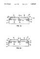
- a waveguide sensor 10is formed on a substrate or chip 12 which contains a light source 14 and a pair of detectors 16,18 integrally formed therein.
- the source 14 and detectors 16,18are linearly aligned, with source 14 at one end; however, different geometries can also be used.
- a waveguide 20 formed of a reference arm 22 and sensing arm 24is mounted on substrate 12 in alignment with source 14 and detectors 16,18. Arms 22,24 are separated by beam splitter 26. Beam splitter 26 is formed by abutting the sloped ends of reference arm 22 and sensing arm 24, and applying suitable optical coatings to produce desired reflection and transmission.
- Beam splitter 26reflects a portion of the light down to the underlying reference detector 16 and transmits the remainder of the light through sensing arm 24 which has a sensing chemistry 30 coated on a portion thereof.
- the light beam passing through sensing arm 24is affected by sensing chemistry 30 as it interacts with a sample.
- sensing chemistriescan be used, including absorption, fluorescence and refractive index.
- the resulting lightis incident on sloped reflective end face 32 which reflects the light downward onto detector 18.
- Reference arm 22is covered by coating 23.
- the substrate 12is preferably a molded semiconductor chip package.
- Source 14is typically an LED or laser diode.
- Detectors 16,18are typically photodiodes (e.g., silicon photodiodes).
- the source 14 and detectors 16,18are integrally formed in the chip package but are not on the surface thereof.
- the chip packageis made of optically transparent material and also protects the source and detectors from the environment.
- FIG. 1Cshows a waveguide sensor 11 which is similar to sensor 10 of FIGS. 1A,B except that sensing arm 24 is replaced with sensing arm 25 which is formed of the sensing chemistry, i.e., sensing chemistry is not just coated on arm 24 of FIG. 1A but the entire arm 25 is made of sensing chemistry.
- sensing arm 24is replaced with sensing arm 25 which is formed of the sensing chemistry, i.e., sensing chemistry is not just coated on arm 24 of FIG. 1A but the entire arm 25 is made of sensing chemistry.
- Thisis particularly advantageous in an absorption type or fluorescence type sensor, since the light will pass through considerably more sensing chemistry than if a surface coating is used. In the case of absorption, the effective path length is increased, and in the case of fluorescence more of the fluorescing wavelength is trapped in the waveguide, thereby giving greater change in the signal.
- the sloped reflective end face 32 of FIG. 1Ais replaced by reflective element 33 (e.g. a
- FIGS. 2A,Bshow a waveguide sensor 15 which is a variation of the sensor 10 of FIGS. 1A,B.
- sensor 15the position of the light source 14 and reference detector 16 are reversed, i.e., the arrangement is still linear but the source 14 is in the center instead of at the end.
- Reference arm 22has a sloped reflective end face 29 positioned over source 14 for inputting a portion of the light into arm 22. The light passes along arm 22 to sloped reflective end face 28 which reflects the light down to reference detector 16.
- Sensing arm 24 of FIGS. 1A,Bis replaced by sensing arm 27 which has sensing chemistry 30 coated on a portion thereof.
- Sensing arm 27has a sloped reflective end face 31 over source 14 which inputs a portion of the light from source 14 into sensing arm 27. After the light interacts with sensing chemistry 30, it is reflected by sloped reflective end face 32 down into detector 18.
- FIG. 2Cshows a waveguide sensor 17 which is similar to sensor 15 of FIGS. 2A,B except that sensing arm 27 is replaced with a sensing arm 34 which is formed of the sensing chemistry.
- the sloped reflective end faces 31,32 of FIGS. 2A,Bare replaced by reflective elements 35,36 (e.g., prisms) that reflect light into and out of arm 34.
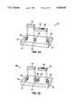
- FIGS. 3A-Cshow a sensor 58 with multiple waveguides on a chip 56.
- three different waveguides (sensing arms) 60,62,64are used. This permits three different chemistries 30a,b,c to be used at once and also provides for a reference channel 66.
- the systemuses a single light source 68 and multiple detectors 70,72,74.
- a fourth detector 76can be used to look at the reference channel 66.
- Light from source 68 in chip 56is incident on sloped reflective end face 61 of waveguide 59 which reflects the light down the waveguide 59 to beam splitter 71. Beam splitter 71 reflects a portion of the light to reference detector 76.
- Beam splitters 73,75divide the transmitted light into the three waveguides 60,62,64 which are coated with a sensing chemistry 30a,b,c, respectively.
- This arrangementcan be used in two approaches: (1) Three different analytes can be analyzed simultaneously or (2) If there is a question of specificity, then coincident or redundant analyses can be accomplished using two or more sensing chemistries which respond to the target analyte.
- the number of waveguides that can be usedis only restricted by source strength and geometric considerations.
- FIG. 3Dshows a multiple waveguide sensor 77 which is similar to sensor 58 of FIGS. 3A-C except that sensing arms 60,62,64 are replaced by sensing arms 78,79,80 which are formed of the sensing chemistry and sloped reflective end faces 63,65,67 are replaced by reflective elements 81,82,83 (e.g., prisms).
- sensing arms 60,62,64are replaced by sensing arms 78,79,80 which are formed of the sensing chemistry and sloped reflective end faces 63,65,67 are replaced by reflective elements 81,82,83 (e.g., prisms).
- FIG. 3Eillustrates the construction of the multi-arm waveguide sensor 58 of FIGS. 3A-C.
- Waveguide 59 with reference channel 66has a flat end face 84 distal from sloped end 61.
- Waveguide 60is placed at right angles to waveguide 59 abutting end face 84.
- the end of waveguide 60 distal from sloped end 63is sloped to form beam splitter 73.
- a matching prism 85is placed against the sloped end of waveguide 60 (beam splitter 73) to form a flat face against which waveguide 64 is placed as right angles.
- the end of waveguide 64 distal from sloped end 67is sloped to form beam splitter 75.
- Waveguide 62has a sloped end face, at the end distal from sloped end 65, which matches the sloped end (beam splitter 75) of waveguide 64, so that waveguide 62 is aligned with waveguide 59.
- Beam splitters 73,75are formed by applying suitable optical coatings to the ends of waveguides 60,62,64 to produce the desired reflection and transmission characteristics.
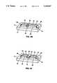
- FIG. 3Fillustrates a waveguide sensor 86 formed on a substrate or chip 56 which is similar to sensor 58 of FIGS. 3A-C but which has multiple sources and a single detector.
- Detectors 70,72,74 of sensor 58are replaced by three sources 90,92,94, typically at three different wavelengths, and source 68 is replaced by a detector 88 which is sufficiently broadband to detect light from all three sources 90,92,94.
- Beam splitter 73is highly reflective to the wavelength of source 90 and highly transmissive to the wavelengths from sources 92,94.
- Beam splitter 75is highly reflective to the wavelength of source 94 and highly transmissive to the wavelength of source 92. The beam splitter characteristics are obtained by suitable optical coatings.
- Sloped end faces 63, 65,67direct light from sources 90,92,94 down waveguides 60,62,64 and beam splitters 73,75 direct the light beams into waveguide (sensing and reference arm) 59.
- Waveguide 59includes beam splitter 91 which directs a portion of the light to reference detector 96. The rest of the light beam passes through waveguide 59 which is coated with (or contains) sensing chemistry 30. The modulated beam is then reflected by end face 61 down to detector 88.
- Waveguides 60,62,64do not contain any sensing chemistry.
- FIGS. 3G,Hshow an alternate embodiment of sensor 86 of FIG. 3F which has multiple sources and multiple sensing chemistries.
- Waveguide sensor 87 on chip 56has three sources 90,92,94, typically at three wavelengths, and a detector 88. Sloped end faces 63,65,67 direct light from sources 90,92,94 into waveguides 60,62,64 where the light first encounters a beam splitter 93,95,97 which directs a portion of the light down to reference detectors 51,52,53. The remainder of the light passes down waveguides 60,62,64 which are coated with (or contain) sensing chemistry 30a,b,c.
- Beam splitters 73,75pass or direct the modulated light beams from waveguides 60,62,64 to waveguide 59, where the light is reflected at end face 61 down to detector 88.
- waveguide sensorscan be formed as described above by mounting waveguide structures on a molded chip package which contains the source(s) and detector(s), it is also possible according to the invention to further integrate the waveguide structures into the molded chip package.
- the waveguide structures of FIGS. 1A-3Hcan be molded as part of the substrate or chip package 12 or 56. It is also possible to form parts of the waveguide structures, as illustrated in FIGS. 4A-H.
- the elements defining the direction of light propagationare formed with the chip as part of the chip fabrication process. Only very simple elements need then be inserted to form a working sensor and these elements are easily interchanged to produce a wide variety of sensors. The design even provides for liquid waveguides, enabling the use of liquid sensing chemistries.
- chip 12 with source 14 and detectors 16,18is formed with waveguide defining elements 36,38,39 formed integrally thereon, i.e., when chip 12 is molded, elements 36,38,39 are formed as part of the molding process.
- Elements 38,39,36are formed over source 14 and detectors 16,18, respectively.
- Source 14is at one end of the linear arrangement.
- Elements 36,38are corner reflectors and element 39 is a beam splitter.
- a waveguide body 41can be easily inserted between elements 38,39 and a waveguide body 42, which is coated with sensing chemistry 30 (or alternatively is partly formed of the sensing chemistry) can be easily inserted between elements 39,36 to form a waveguide sensor 37.
- sensing chemistry 30or alternatively is partly formed of the sensing chemistry
- FIGS. 4C,Dare top and side sectional views. Inserts 41,42 of FIG. 4A can be inserted in channels 45,46 or channels 45,46 can be filled with liquid reagents and then covered with a membrane 50, as shown in FIG. 4D. Membrane 50 can be attached to side walls 44.
- FIG. 4Eshows an alternate embodiment of a chip 12 with integral waveguide defining elements 35,36,38,39.
- source 14is in the center with detectors 16,18 at the ends.
- elements 35,36,38,39which are corner reflectors, are formed as part of the fabrication process of chip 12.
- a waveguide body 41can be easily inserted between elements 38,39 and a waveguide body 43 which is coated with (or contains) a sensing chemistry 30, can be easily inserted between elements 35,36 to form a waveguide sensor 40.
- the spaces between elements 35,36,38,39can be enclosed by lateral walls 44, defining channels 47,48.
- FIGS. 4G-Hare top and side sectional views. Inserts 41,43 of FIG. 4E can be inserted in channels 47,48 or channels 47,48 can be filled with liquid reagents and then covered with a membrane 50, as shown in FIG. 4H. Membrane 50 can be attached to side walls 44.
- the molded integrated chip package 12which contains the source 14 and detectors 16,18 can also include other electronics, as shown in FIGS. 1A,2A. Associated with each detector 16,18 can be an amplifier 98 or other signal processing electronics. A feedback circuit 99 can also be included, connected between source 14 and reference detector 16 to maintain a constant source output.
Landscapes
- Physics & Mathematics (AREA)
- General Physics & Mathematics (AREA)
- Chemical & Material Sciences (AREA)
- General Health & Medical Sciences (AREA)
- Pathology (AREA)
- Health & Medical Sciences (AREA)
- Analytical Chemistry (AREA)
- Biochemistry (AREA)
- Optics & Photonics (AREA)
- Immunology (AREA)
- Life Sciences & Earth Sciences (AREA)
- Engineering & Computer Science (AREA)
- Chemical Kinetics & Catalysis (AREA)
- Plasma & Fusion (AREA)
- Investigating Or Analysing Materials By Optical Means (AREA)
- Investigating Or Analysing Materials By The Use Of Chemical Reactions (AREA)
- Investigating, Analyzing Materials By Fluorescence Or Luminescence (AREA)
Abstract
Description
The invention relates generally to optical chemical sensors, and more particularly to optical waveguide chemical sensors.
A variety of optical chemical sensors based on optical fibers and other waveguides have been developed. U.S. Pat. No. 5,165,005 to Klainer et al, shows a planar waveguide structure with a thin film metal coating. An external source and detector are optically coupled to the waveguide.
A problem with the prior art is that the entire sensor is not integrated, i.e., external source and detector and the entire waveguide must be replaced for a different sensing chemistry. Accordingly, it would be desirable to provide a waveguide chemical sensor with integrated structure and in which the sensing chemistry can be easily changed.
Accordingly, it is an object of the invention to provide a waveguide chemical sensor with an integrated structure.
It is also an object of the invention to provide a waveguide chemical sensor with interchangeable sensing chemistries.
The invention is a waveguide chemical sensor having at least one waveguide arm mounted on a substrate or chip having at least one source and at least one detector formed integrally therein. The waveguide arms can be fixedly mounted on the substrate (e.g., by gluing) or removably attached (e.g., by mechanical clips). The waveguide arms, or parts thereof, can also be formed (e.g., molded) as part of the substrate or chip itself. A reference channel can be included. Different sensing arms can be coated with or formed of different sensing chemistries. Reflective end faces of the waveguide arms direct light transmitted therethrough to a detector in the substrate.
FIGS. 1A, B are side and perspective views of a waveguide sensor having a reference arm and sensing arm.
FIG. 1C is a perspective view of the waveguide sensor of FIGS. 1A,B wherein the sensing arm waveguide is formed of the sensing chemistry.
FIGS. 2A, B are side and perspective views of an alternate embodiment of a waveguide sensor having a reference arm and sensing arm.
FIG. 2C is a perspective view of the waveguide sensor of FIGS. 2A,B wherein the sensing arm waveguide is formed of the sensing chemistry.
FIGS. 3A-C show a multiple arm waveguide sensor.
FIG. 3D shows an alternate embodiment of the waveguide sensor of FIGS. 3A-C wherein the sensing arms are formed of sensing chemistries.
FIG. 3E is a top view of the waveguide sensor of FIGS. 3A-C showing the assembly of the waveguide arms.
FIG. 3F shows a multiple arm waveguide sensor with multiple sources.
FIGS. 3G,H show an alternate embodiment of a multiple arm waveguide sensor with multiple sources.
FIGS. 4A-D show of a molded chip package with integral waveguide forming elements.
FIGS. 4E-H show an alternate embodiment of a molded chip package with integral waveguide forming elements.
As shown in FIGS. 1A,B, awaveguide sensor 10 is formed on a substrate orchip 12 which contains alight source 14 and a pair ofdetectors source 14 anddetectors source 14 at one end; however, different geometries can also be used. Awaveguide 20 formed of areference arm 22 and sensingarm 24 is mounted onsubstrate 12 in alignment withsource 14 anddetectors Arms beam splitter 26.Beam splitter 26 is formed by abutting the sloped ends ofreference arm 22 and sensingarm 24, and applying suitable optical coatings to produce desired reflection and transmission. Light fromsource 14 under slopedreflective end face 28 is incident thereon and reflects to send a light beam downwaveguide 20.Beam splitter 26 reflects a portion of the light down to theunderlying reference detector 16 and transmits the remainder of the light through sensingarm 24 which has asensing chemistry 30 coated on a portion thereof. The light beam passing through sensingarm 24 is affected by sensingchemistry 30 as it interacts with a sample. Various types of sensing chemistries can be used, including absorption, fluorescence and refractive index. The resulting light is incident on slopedreflective end face 32 which reflects the light downward ontodetector 18.Reference arm 22 is covered bycoating 23.
As shown in FIG. 1A, thesubstrate 12 is preferably a molded semiconductor chip package.Source 14 is typically an LED or laser diode.Detectors source 14 anddetectors
FIG. 1C shows awaveguide sensor 11 which is similar tosensor 10 of FIGS. 1A,B except thatsensing arm 24 is replaced with sensingarm 25 which is formed of the sensing chemistry, i.e., sensing chemistry is not just coated onarm 24 of FIG. 1A but theentire arm 25 is made of sensing chemistry. This is particularly advantageous in an absorption type or fluorescence type sensor, since the light will pass through considerably more sensing chemistry than if a surface coating is used. In the case of absorption, the effective path length is increased, and in the case of fluorescence more of the fluorescing wavelength is trapped in the waveguide, thereby giving greater change in the signal. The sloped reflective end face 32 of FIG. 1A is replaced by reflective element 33 (e.g. a prism) to reflect light passing througharm 25 intodetector 18.
FIGS. 2A,B show awaveguide sensor 15 which is a variation of thesensor 10 of FIGS. 1A,B. Insensor 15, the position of thelight source 14 andreference detector 16 are reversed, i.e., the arrangement is still linear but thesource 14 is in the center instead of at the end.Reference arm 22 has a sloped reflective end face 29 positioned oversource 14 for inputting a portion of the light intoarm 22. The light passes alongarm 22 to sloped reflective end face 28 which reflects the light down toreference detector 16.Sensing arm 24 of FIGS. 1A,B is replaced by sensingarm 27 which hassensing chemistry 30 coated on a portion thereof.Sensing arm 27 has a sloped reflective end face 31 oversource 14 which inputs a portion of the light fromsource 14 intosensing arm 27. After the light interacts withsensing chemistry 30, it is reflected by sloped reflective end face 32 down intodetector 18.
FIG. 2C shows awaveguide sensor 17 which is similar tosensor 15 of FIGS. 2A,B except thatsensing arm 27 is replaced with asensing arm 34 which is formed of the sensing chemistry. The sloped reflective end faces 31,32 of FIGS. 2A,B are replaced byreflective elements 35,36 (e.g., prisms) that reflect light into and out ofarm 34.
FIGS. 3A-C show asensor 58 with multiple waveguides on achip 56. In the arrangement shown, three different waveguides (sensing arms) 60,62,64 are used. This permits threedifferent chemistries 30a,b,c to be used at once and also provides for areference channel 66. The system uses a singlelight source 68 andmultiple detectors fourth detector 76 can be used to look at thereference channel 66. Light fromsource 68 inchip 56 is incident on sloped reflective end face 61 ofwaveguide 59 which reflects the light down thewaveguide 59 tobeam splitter 71.Beam splitter 71 reflects a portion of the light toreference detector 76.Beam splitters waveguides sensing chemistry 30a,b,c, respectively. The light passing throughwaveguides chemistries 30a,b,c, then is reflected by sloped reflective end faces 63,65,67 intodetectors
FIG. 3D shows amultiple waveguide sensor 77 which is similar tosensor 58 of FIGS. 3A-C except that sensingarms arms reflective elements 81,82,83 (e.g., prisms).
FIG. 3E illustrates the construction of themulti-arm waveguide sensor 58 of FIGS. 3A-C. Waveguide 59 withreference channel 66 has aflat end face 84 distal fromsloped end 61.Waveguide 60 is placed at right angles to waveguide 59abutting end face 84. The end ofwaveguide 60 distal fromsloped end 63 is sloped to formbeam splitter 73. A matchingprism 85 is placed against the sloped end of waveguide 60 (beam splitter 73) to form a flat face against which waveguide 64 is placed as right angles. The end ofwaveguide 64 distal fromsloped end 67 is sloped to formbeam splitter 75.Waveguide 62 has a sloped end face, at the end distal fromsloped end 65, which matches the sloped end (beam splitter 75) ofwaveguide 64, so thatwaveguide 62 is aligned withwaveguide 59.Beam splitters waveguides
FIG. 3F illustrates awaveguide sensor 86 formed on a substrate orchip 56 which is similar tosensor 58 of FIGS. 3A-C but which has multiple sources and a single detector.Detectors sensor 58 are replaced by threesources source 68 is replaced by adetector 88 which is sufficiently broadband to detect light from all threesources Beam splitter 73 is highly reflective to the wavelength ofsource 90 and highly transmissive to the wavelengths fromsources Beam splitter 75 is highly reflective to the wavelength ofsource 94 and highly transmissive to the wavelength ofsource 92. The beam splitter characteristics are obtained by suitable optical coatings. Sloped end faces 63, 65,67 direct light fromsources waveguides beam splitters Waveguide 59 includesbeam splitter 91 which directs a portion of the light toreference detector 96. The rest of the light beam passes throughwaveguide 59 which is coated with (or contains) sensingchemistry 30. The modulated beam is then reflected byend face 61 down todetector 88. Thus, in this configuration, there is only one sensing chemistry but three different light sources.Waveguides
FIGS. 3G,H show an alternate embodiment ofsensor 86 of FIG. 3F which has multiple sources and multiple sensing chemistries.Waveguide sensor 87 onchip 56 has threesources detector 88. Sloped end faces 63,65,67 direct light fromsources waveguides beam splitter reference detectors waveguides sensing chemistry 30a,b,c.Beam splitters waveguides waveguide 59, where the light is reflected atend face 61 down todetector 88. Thus, in this configuration, there is a sensing chemistry on each arm with a source, but there is also a reference detector on each sensing arm.
Although waveguide sensors can be formed as described above by mounting waveguide structures on a molded chip package which contains the source(s) and detector(s), it is also possible according to the invention to further integrate the waveguide structures into the molded chip package. The waveguide structures of FIGS. 1A-3H can be molded as part of the substrate orchip package
As shown in FIG. 4A,chip 12 withsource 14 anddetectors waveguide defining elements chip 12 is molded,elements Elements source 14 anddetectors Source 14 is at one end of the linear arrangement.Elements element 39 is a beam splitter. Awaveguide body 41 can be easily inserted betweenelements waveguide body 42, which is coated with sensing chemistry 30 (or alternatively is partly formed of the sensing chemistry) can be easily inserted betweenelements waveguide sensor 37. As shown in FIG. 4B, the spaces betweenelements lateral walls 44, definingchannels Inserts channels channels membrane 50, as shown in FIG. 4D.Membrane 50 can be attached toside walls 44.
FIG. 4E shows an alternate embodiment of achip 12 with integralwaveguide defining elements source 14 is in the center withdetectors elements chip 12. Awaveguide body 41 can be easily inserted betweenelements waveguide body 43 which is coated with (or contains) asensing chemistry 30, can be easily inserted betweenelements waveguide sensor 40. As shown in FIG. 4F, the spaces betweenelements lateral walls 44, definingchannels Inserts channels channels membrane 50, as shown in FIG. 4H.Membrane 50 can be attached toside walls 44.
The moldedintegrated chip package 12 which contains thesource 14 anddetectors detector amplifier 98 or other signal processing electronics. Afeedback circuit 99 can also be included, connected betweensource 14 andreference detector 16 to maintain a constant source output.
Changes and modifications in the specifically described embodiments can be carried out without departing from the scope of the invention which is intended to be limited only by the scope of the appended claims.
Claims (22)
1. An optical waveguide chemical sensor comprising:
a modular substrate having at least one light source and at least one light detector formed internally therein and covered by an optically transparent material;
a waveguide structure mounted on said substrate and extending over said at least one source and at least one detector, said waveguide structure including direction turning means for guiding light from said at least one source into said waveguide structure and direction turning means for guiding light from said waveguide structure to said at least one detector; and
a sensing chemistry formed on or in a portion of the waveguide structure.
2. The sensor of claim 1 wherein the modular substrate has one source and first and second detectors in a linear arrangement with the source at one end, and the waveguide structure is formed of a first waveguide body which extends from said source to the first detector and a second waveguide body forming a junction with the first waveguide body and extending between the first and second detectors.
3. The sensor of claim 2 wherein the direction turning means for guiding light from the source into the waveguide structure comprises a sloped reflective end face formed on the first waveguide body, and the direction turning means for guiding light from the waveguide structure to the first and second detectors comprises a beam splitter formed at the junction between the first and second waveguide bodies and a sloped reflective end face formed at the distal end of the second waveguide body.
4. The sensor of claim 3 wherein the sensing chemistry is formed on or in the second waveguide body, and the first detector forms a reference detector.
5. The sensor of claim 1 wherein the modular substrate has one source and two detectors in a linear arrangement with the source located between the two detectors, and the waveguide structure is formed of a first waveguide body which extends from said source to one detector and an adjacent second waveguide body which extends from said source to the other detector.
6. The sensor of claim 5 wherein the direction turning means for guiding light from the source into the waveguide structure comprises a sloped reflective end face formed on one end of each waveguide body and the direction turning means for guiding light from the waveguide structure to the detectors comprises a sloped reflective end face formed on an end of each waveguide body distal from said one end.
7. The sensor of claim 6 wherein the sensing chemistry is formed on or in one waveguide body and the other waveguide body forms a reference arm.
8. The sensor of claim 1 wherein the modular substrate has one source and a plurality of detectors in a geometric pattern, and the waveguide structure comprises a plurality of interconnected arms extending from the detectors to the source.
9. The sensor of claim 8 wherein a sensing chemistry is formed on or in each arm which extends to a detector.
10. The sensor of claim 9 wherein each arm which extends to a detector has a different sensing chemistry formed thereon or therein.
11. The sensor of claim 8 wherein the modular substrate has one source and three detectors and the waveguide structure comprises a first waveguide arm extending from the source and three sensing arms extending from the first waveguide arm to a respective detector, one sensing arm being aligned with the first waveguide arm and two being orthogonal, and further comprising a pair of beam splitters formed in the sensing arms for splitting light from the source among the three sensing arms.
12. The sensor of claim 11 further comprising a beam splitter in the first waveguide arm and a reference detector below the beam splitter.
13. The sensor of claim 1 wherein the modular substrate has one detector and a plurality of sources in a geometric pattern, and the waveguide structure comprises a plurality of interconnected arms extending from the sources to the detector.
14. The sensor of claim 13 wherein the sensing chemistry is formed on or in an arm of the waveguide structure near the detector, and further comprising a beam splitter located between the waveguide arms from the sources and the sensing chemistry and a reference detector below the beam splitter.
15. The sensor of claim 13 wherein a sensing chemistry is formed on or in each arm which extends to a source, and further comprising a beam splitter in each said arm between the source and sensing chemistry and a reference detector below each beam splitter.
16. The sensor of claim 1 wherein the modular substrate is a semiconductor chip package.
17. The sensor of claim 1 wherein the waveguide structure is molded as part of the modular substrate.
18. The sensor of claim 1 wherein the direction turning means for guiding light from said at least one source and the direction turning means for guiding light to said at least one detector are molded as part of the modular substrate.
19. The sensor of claim 18 further comprising removable waveguide body inserts which fit between said guiding means.
20. The sensor of claim 19 wherein the sensing chemistry is formed on or in a waveguide body insert.
21. The sensor of claim 18 further comprising lateral walls defining open channels between said guiding means.
22. The sensor of claim 21 further comprising a liquid reagent which forms the sensing chemistry filling said open channels and a membrane covering said liquid reagent filled channels.
Priority Applications (10)
| Application Number | Priority Date | Filing Date | Title |
|---|---|---|---|
| US08/201,796US5439647A (en) | 1994-02-25 | 1994-02-25 | Chip level waveguide sensor |
| CA002183228ACA2183228A1 (en) | 1994-02-25 | 1995-02-27 | Chip level waveguide sensor |
| JP07522500AJP3139770B2 (en) | 1994-02-25 | 1995-02-27 | Chip-level waveguide sensor |
| PCT/US1995/002377WO1995023333A1 (en) | 1994-02-25 | 1995-02-27 | Chip level waveguide sensor |
| EP95911114AEP0746759A1 (en) | 1994-02-25 | 1995-02-27 | Chip level waveguide sensor |
| DE0746759TDE746759T1 (en) | 1994-02-25 | 1995-02-27 | WAVE LEAD SENSOR ON CHIP LEVEL |
| TW084101920ATW310378B (en) | 1994-02-25 | 1995-03-01 | |
| US08/511,959US5650123A (en) | 1994-02-25 | 1995-08-07 | Chip level waveguide sensor |
| US08/587,231US5737457A (en) | 1994-02-25 | 1996-01-16 | Chip level waveguide sensor |
| KR1019960704589AKR970701344A (en) | 1994-02-25 | 1996-08-21 | CHIP LEVEL WA VEGUIDE SENSOR |
Applications Claiming Priority (1)
| Application Number | Priority Date | Filing Date | Title |
|---|---|---|---|
| US08/201,796US5439647A (en) | 1994-02-25 | 1994-02-25 | Chip level waveguide sensor |
Related Child Applications (2)
| Application Number | Title | Priority Date | Filing Date |
|---|---|---|---|
| US08/511,959ContinuationUS5650123A (en) | 1994-02-25 | 1995-08-07 | Chip level waveguide sensor |
| US08/511,959Continuation-In-PartUS5650123A (en) | 1994-02-25 | 1995-08-07 | Chip level waveguide sensor |
Publications (1)
| Publication Number | Publication Date |
|---|---|
| US5439647Atrue US5439647A (en) | 1995-08-08 |
Family
ID=22747336
Family Applications (2)
| Application Number | Title | Priority Date | Filing Date |
|---|---|---|---|
| US08/201,796Expired - Fee RelatedUS5439647A (en) | 1994-02-25 | 1994-02-25 | Chip level waveguide sensor |
| US08/511,959Expired - LifetimeUS5650123A (en) | 1994-02-25 | 1995-08-07 | Chip level waveguide sensor |
Family Applications After (1)
| Application Number | Title | Priority Date | Filing Date |
|---|---|---|---|
| US08/511,959Expired - LifetimeUS5650123A (en) | 1994-02-25 | 1995-08-07 | Chip level waveguide sensor |
Country Status (8)
| Country | Link |
|---|---|
| US (2) | US5439647A (en) |
| EP (1) | EP0746759A1 (en) |
| JP (1) | JP3139770B2 (en) |
| KR (1) | KR970701344A (en) |
| CA (1) | CA2183228A1 (en) |
| DE (1) | DE746759T1 (en) |
| TW (1) | TW310378B (en) |
| WO (1) | WO1995023333A1 (en) |
Cited By (61)
| Publication number | Priority date | Publication date | Assignee | Title |
|---|---|---|---|---|
| WO1997006426A1 (en)* | 1995-08-04 | 1997-02-20 | E.I. Du Pont De Nemours And Company | Waveguide sensing element for use in a sample medium and method of launching electromagnetic radiation |
| US5619599A (en)* | 1995-05-12 | 1997-04-08 | Xerox Corporation | Remote split scan detector |
| US5650123A (en)* | 1994-02-25 | 1997-07-22 | Fci-Fiberchem, Inc. | Chip level waveguide sensor |
| US5671303A (en)* | 1996-04-17 | 1997-09-23 | Motorola, Inc. | Molecular detection apparatus and method using optical waveguide detection |
| FR2747786A1 (en)* | 1996-04-17 | 1997-10-24 | Motorola Inc | INTEGRATED DEVICE FOR OPTICAL MOLECULAR DETECTION AND METHOD FOR SAME |
| DE19647644A1 (en)* | 1996-11-18 | 1998-05-20 | Fraunhofer Ges Forschung | Micromechanical transmission measuring cell and reactor for sample fluid |
| US5766956A (en)* | 1997-05-27 | 1998-06-16 | American Research Corporation | Diode laser-based chemical and biological sensor |
| US5779978A (en)* | 1996-02-29 | 1998-07-14 | Avl Medical Instruments Ag | Measuring assembly for luminescence analysis |
| US5854868A (en)* | 1994-06-22 | 1998-12-29 | Fujitsu Limited | Optical device and light waveguide integrated circuit |
| EP0834735A3 (en)* | 1996-10-01 | 1999-08-11 | Texas Instruments Inc. | A sensor |
| EP0990135A4 (en)* | 1996-04-30 | 2000-04-26 | Metrika Inc | Method and device for measuring reflected optical radiation |
| US6060022A (en)* | 1996-07-05 | 2000-05-09 | Beckman Coulter, Inc. | Automated sample processing system including automatic centrifuge device |
| US6110749A (en)* | 1996-03-01 | 2000-08-29 | Beckman Coulter, Inc. | System for simultaneously conducting multiple ligand binding assays |
| US6149591A (en)* | 1997-02-21 | 2000-11-21 | Duke University | Refractometric devices especially adapted for the in vivo detection of refractive indices of cervical mucus |
| WO2001038854A1 (en)* | 1999-11-26 | 2001-05-31 | Associates Of Cape Cod, Inc. | Pyros kinetix reader for conducting assays |
| DE19953338A1 (en)* | 1999-11-05 | 2001-05-31 | Univ Jw Goethe Frankfurt Main | Measurement cell for infrared spectroscopy has permeable mirror provided between sample area and sample medium container |
| US6277651B1 (en) | 1998-07-09 | 2001-08-21 | Calspan Srl Corporation | Diode laser electrochemical sensor for detecting chemical and biological analytes |
| US6369893B1 (en) | 1998-05-19 | 2002-04-09 | Cepheid | Multi-channel optical detection system |
| US6438279B1 (en) | 1999-01-07 | 2002-08-20 | Cornell Research Foundation, Inc. | Unitary microcapiliary and waveguide structure and method of fabrication |
| US20020136503A1 (en)* | 2001-03-26 | 2002-09-26 | Kole Marcus Egbert | Sensor for a receiving device for cooperation with an optical fiber |
| US6490034B1 (en) | 1996-11-18 | 2002-12-03 | Fraunhofer-Gesellschaft Zur Foerderung Der Angewandten Forschung E.V. | Micromechanical transmission measuring cell |
| US6509195B1 (en)* | 1997-06-09 | 2003-01-21 | Csem Centre Suisse D'electronique Et De Microtechnique Sa | Electrochemoluminescent detector |
| WO2003050519A1 (en)* | 2001-12-11 | 2003-06-19 | Sensors For Medicine And Science, Inc. | High performance fluorescent optical sensor |
| US20030222223A1 (en)* | 2002-06-03 | 2003-12-04 | Toshihiro Kamei | Solid-state detector and optical system for microchip analyzers |
| US6694067B1 (en) | 2001-01-05 | 2004-02-17 | Los Gatos Research | Cavity enhanced fiber optic and waveguide chemical sensor |
| US20040218288A1 (en)* | 2003-05-02 | 2004-11-04 | International Business Machines Corporation | Optical communication assembly |
| US20040217464A1 (en)* | 2003-05-02 | 2004-11-04 | International Business Machines Corporation | Optical assemblies for transmitting and manipulating optical beams |
| EP1510808A1 (en)* | 2003-09-01 | 2005-03-02 | Seiko Epson Corporation | Biosensor and method of manufacturing biosensor |
| US20050106746A1 (en)* | 1999-11-26 | 2005-05-19 | Associates Of Cape Cod, Inc. | Reader for conducting assays |
| US20060051244A1 (en)* | 2002-09-27 | 2006-03-09 | Mirko Lehmann | Device for the detection of at least one ligand contained in a sample that is to be analyzed |
| US20060063984A1 (en)* | 2004-07-26 | 2006-03-23 | Kenichi Uchiyama | Optical waveguide type iontophoresis sensor chip and method for packaging sensor chip |
| US7150995B2 (en) | 2004-01-16 | 2006-12-19 | Metrika, Inc. | Methods and systems for point of care bodily fluid analysis |
| US20070045521A1 (en)* | 2005-08-23 | 2007-03-01 | Fuji Xerox Co., Ltd. | Optical distribution module and signal processing device |
| US20070211985A1 (en)* | 2006-03-10 | 2007-09-13 | Plc Diagnostics, Inc. | Optical Scanning System |
| US20080152281A1 (en)* | 2006-09-01 | 2008-06-26 | Pacific Biosciences Of California, Inc. | Substrates, systems and methods for analyzing materials |
| US20090232443A1 (en)* | 2005-02-28 | 2009-09-17 | Nec Corporation | Connection structure of two-dimensional array optical element and optical circuit |
| US20100065726A1 (en)* | 2006-09-01 | 2010-03-18 | Pacific Biosciences Of California, Inc. | Substrates and optical systems and methods of use thereof |
| US8207509B2 (en) | 2006-09-01 | 2012-06-26 | Pacific Biosciences Of California, Inc. | Substrates, systems and methods for analyzing materials |
| US8288157B2 (en) | 2007-09-12 | 2012-10-16 | Plc Diagnostics, Inc. | Waveguide-based optical scanning systems |
| US20130149197A1 (en)* | 2011-12-09 | 2013-06-13 | National Taiwan University Of Science And Technology | Biotechnology Detecting Device with Optical Fibers and LEDs |
| US8465699B2 (en) | 2010-02-19 | 2013-06-18 | Pacific Biosciences Of California, Inc. | Illumination of integrated analytical systems |
| US8675199B2 (en) | 2006-03-10 | 2014-03-18 | Plc Diagnostics, Inc. | Waveguide-based detection system with scanning light source |
| US8747751B2 (en) | 2008-06-16 | 2014-06-10 | Plc Diagnostics, Inc. | System and method for nucleic acids sequencing by phased synthesis |
| US8837872B2 (en) | 2010-12-30 | 2014-09-16 | Qualcomm Incorporated | Waveguide structures for signal and/or power transmission in a semiconductor device |
| US20150042985A1 (en)* | 2012-02-21 | 2015-02-12 | Entegris-Jetalon Solutions, Inc. | Optical sensor apparatus to detect light based on the refractive index of a sample |
| US20150086425A1 (en)* | 2006-03-07 | 2015-03-26 | Hitachi, Ltd. | Cells for biochemical analysis, kit for biochemical analysis, and biochemical analyzer |
| US8994946B2 (en) | 2010-02-19 | 2015-03-31 | Pacific Biosciences Of California, Inc. | Integrated analytical system and method |
| US9223084B2 (en) | 2012-12-18 | 2015-12-29 | Pacific Biosciences Of California, Inc. | Illumination of optical analytical devices |
| US9372308B1 (en) | 2012-06-17 | 2016-06-21 | Pacific Biosciences Of California, Inc. | Arrays of integrated analytical devices and methods for production |
| US9423397B2 (en) | 2006-03-10 | 2016-08-23 | Indx Lifecare, Inc. | Waveguide-based detection system with scanning light source |
| US20160363728A1 (en)* | 2015-06-12 | 2016-12-15 | Pacific Biosciences Of California, Inc. | Integrated target waveguide devices and systems for optical coupling |
| US9528939B2 (en) | 2006-03-10 | 2016-12-27 | Indx Lifecare, Inc. | Waveguide-based optical scanning systems |
| DE102015217425A1 (en)* | 2015-09-11 | 2017-03-16 | Robert Bosch Gmbh | Light-conducting device, measuring system and method for producing a light-conducting device |
| US9606068B2 (en) | 2014-08-27 | 2017-03-28 | Pacific Biosciences Of California, Inc. | Arrays of integrated analytical devices |
| US9624540B2 (en) | 2013-02-22 | 2017-04-18 | Pacific Biosciences Of California, Inc. | Integrated illumination of optical analytical devices |
| US9976192B2 (en) | 2006-03-10 | 2018-05-22 | Ldip, Llc | Waveguide-based detection system with scanning light source |
| US10018566B2 (en) | 2014-02-28 | 2018-07-10 | Ldip, Llc | Partially encapsulated waveguide based sensing chips, systems and methods of use |
| US10302972B2 (en) | 2015-01-23 | 2019-05-28 | Pacific Biosciences Of California, Inc. | Waveguide transmission |
| US10487356B2 (en) | 2015-03-16 | 2019-11-26 | Pacific Biosciences Of California, Inc. | Integrated devices and systems for free-space optical coupling |
| US11181479B2 (en) | 2015-02-27 | 2021-11-23 | Ldip, Llc | Waveguide-based detection system with scanning light source |
| US11983790B2 (en) | 2015-05-07 | 2024-05-14 | Pacific Biosciences Of California, Inc. | Multiprocessor pipeline architecture |
Families Citing this family (17)
| Publication number | Priority date | Publication date | Assignee | Title |
|---|---|---|---|---|
| US5894535A (en)* | 1997-05-07 | 1999-04-13 | Hewlett-Packard Company | Optical waveguide device for wavelength demultiplexing and waveguide crossing |
| US5966478A (en)* | 1997-09-17 | 1999-10-12 | Lucent Technologies Inc. | Integrated optical circuit having planar waveguide turning mirrors |
| US6710870B1 (en)* | 1998-02-05 | 2004-03-23 | Novartis Ag | Method and device for measuring luminescence |
| CA2376325A1 (en)* | 1999-08-19 | 2001-03-01 | Yang Zhao | Apparatus and method for visually identifying micro-forces with a palette of cantilever array blocks |
| DE10002329A1 (en) | 2000-01-20 | 2001-08-02 | Infineon Technologies Ag | Manufacturing process for an optical transmitter assembly |
| US7524459B2 (en)* | 2002-01-24 | 2009-04-28 | California Institute Of Technology In Pasadena | Optoelectronic and microfluidic integration for miniaturized spectroscopic devices |
| US20030154149A1 (en)* | 2002-02-13 | 2003-08-14 | Dilip Gajendragadkar | System and method of creating and executing a restricted stock sale plan |
| US7059782B2 (en)* | 2002-04-12 | 2006-06-13 | Intel Corporation | Suppressing back reflection between optical interfaces |
| JP3952923B2 (en)* | 2002-10-01 | 2007-08-01 | セイコーエプソン株式会社 | Manufacturing method of optical interconnection circuit |
| US7195941B2 (en)* | 2003-03-26 | 2007-03-27 | Intel Corporation | Optical devices and methods to construct the same |
| US7221455B2 (en)* | 2004-01-20 | 2007-05-22 | The Regents Of The Unversity Of California | Integrated, fluorescence-detecting microanalytical system |
| DE102005062174C5 (en)* | 2005-12-23 | 2010-05-06 | INSTITUT FüR MIKROTECHNIK MAINZ GMBH | measuring chip |
| US8472437B2 (en)* | 2010-02-15 | 2013-06-25 | Texas Instruments Incorporated | Wireless chip-to-chip switching |
| JP2013092393A (en)* | 2011-10-24 | 2013-05-16 | Sony Corp | Chemical sensor, biomolecule detection device, and biomolecule detection method |
| EP4528271A1 (en) | 2023-09-22 | 2025-03-26 | Sotax Ag | Dissolution testing apparatus with a common heating channel |
| EP4528270A1 (en) | 2023-09-22 | 2025-03-26 | Sotax Ag | Heating module for heating a dissolution medium of a dissolution testing apparatus |
| EP4528272A1 (en) | 2023-09-22 | 2025-03-26 | Sotax Ag | Dissolution testing apparatus for open or closed loop configuration |
Citations (11)
| Publication number | Priority date | Publication date | Assignee | Title |
|---|---|---|---|---|
| US4005312A (en)* | 1973-11-08 | 1977-01-25 | Lemelson Jerome H | Electro-optical circuits and manufacturing techniques |
| US4136928A (en)* | 1977-05-06 | 1979-01-30 | Bell Telephone Laboratories, Incorporated | Optical integrated circuit including junction laser with oblique mirror |
| US4699449A (en)* | 1985-03-05 | 1987-10-13 | Canadian Patents And Development Limited-Societe Canadienne Des Brevets Et D'exploitation Limitee | Optoelectronic assembly and method of making the same |
| US4708423A (en)* | 1984-09-25 | 1987-11-24 | U.S. Philips Corp. | Optical wave guides and coupling member monolithically integrated on a semiconductor substrate |
| US4872759A (en)* | 1987-07-07 | 1989-10-10 | Siemens Aktiengesellschaft | Sensor for gases or ions |
| US4888785A (en)* | 1988-01-19 | 1989-12-19 | Bell Communications Research, Inc. | Miniature integrated optical beam splitter |
| US5109444A (en)* | 1988-10-04 | 1992-04-28 | Canon Kabushiki Kaisha | Integrated type optical node and optical information system using the same |
| US5165005A (en)* | 1988-01-29 | 1992-11-17 | Fiberchem Inc. | Planar and other waveguide refractive index sensors using metal cladding |
| US5173747A (en)* | 1990-09-20 | 1992-12-22 | Battelle Memorial Institute | Integrated optical directional-coupling refractometer apparatus |
| US5252294A (en)* | 1988-06-01 | 1993-10-12 | Messerschmitt-Bolkow-Blohm Gmbh | Micromechanical structure |
| US5262656A (en)* | 1991-06-07 | 1993-11-16 | Thomson-Csf | Optical semiconductor transceiver with chemically resistant layers |
Family Cites Families (4)
| Publication number | Priority date | Publication date | Assignee | Title |
|---|---|---|---|---|
| ATE77483T1 (en)* | 1986-04-23 | 1992-07-15 | Avl Medical Instr Ag | SENSOR ELEMENT FOR DETERMINING SUBSTANCE CONCENTRATIONS. |
| AT390677B (en)* | 1986-10-10 | 1990-06-11 | Avl Verbrennungskraft Messtech | SENSOR ELEMENT FOR DETERMINING SUBSTANCE CONCENTRATIONS |
| US5082629A (en) | 1989-12-29 | 1992-01-21 | The Board Of The University Of Washington | Thin-film spectroscopic sensor |
| US5439647A (en)* | 1994-02-25 | 1995-08-08 | Fiberchem, Inc. | Chip level waveguide sensor |
- 1994
- 1994-02-25USUS08/201,796patent/US5439647A/ennot_activeExpired - Fee Related
- 1995
- 1995-02-27DEDE0746759Tpatent/DE746759T1/enactivePending
- 1995-02-27EPEP95911114Apatent/EP0746759A1/ennot_activeWithdrawn
- 1995-02-27WOPCT/US1995/002377patent/WO1995023333A1/ennot_activeApplication Discontinuation
- 1995-02-27JPJP07522500Apatent/JP3139770B2/ennot_activeExpired - Fee Related
- 1995-02-27CACA002183228Apatent/CA2183228A1/ennot_activeAbandoned
- 1995-03-01TWTW084101920Apatent/TW310378B/zhactive
- 1995-08-07USUS08/511,959patent/US5650123A/ennot_activeExpired - Lifetime
- 1996
- 1996-08-21KRKR1019960704589Apatent/KR970701344A/ennot_activeCeased
Patent Citations (11)
| Publication number | Priority date | Publication date | Assignee | Title |
|---|---|---|---|---|
| US4005312A (en)* | 1973-11-08 | 1977-01-25 | Lemelson Jerome H | Electro-optical circuits and manufacturing techniques |
| US4136928A (en)* | 1977-05-06 | 1979-01-30 | Bell Telephone Laboratories, Incorporated | Optical integrated circuit including junction laser with oblique mirror |
| US4708423A (en)* | 1984-09-25 | 1987-11-24 | U.S. Philips Corp. | Optical wave guides and coupling member monolithically integrated on a semiconductor substrate |
| US4699449A (en)* | 1985-03-05 | 1987-10-13 | Canadian Patents And Development Limited-Societe Canadienne Des Brevets Et D'exploitation Limitee | Optoelectronic assembly and method of making the same |
| US4872759A (en)* | 1987-07-07 | 1989-10-10 | Siemens Aktiengesellschaft | Sensor for gases or ions |
| US4888785A (en)* | 1988-01-19 | 1989-12-19 | Bell Communications Research, Inc. | Miniature integrated optical beam splitter |
| US5165005A (en)* | 1988-01-29 | 1992-11-17 | Fiberchem Inc. | Planar and other waveguide refractive index sensors using metal cladding |
| US5252294A (en)* | 1988-06-01 | 1993-10-12 | Messerschmitt-Bolkow-Blohm Gmbh | Micromechanical structure |
| US5109444A (en)* | 1988-10-04 | 1992-04-28 | Canon Kabushiki Kaisha | Integrated type optical node and optical information system using the same |
| US5173747A (en)* | 1990-09-20 | 1992-12-22 | Battelle Memorial Institute | Integrated optical directional-coupling refractometer apparatus |
| US5262656A (en)* | 1991-06-07 | 1993-11-16 | Thomson-Csf | Optical semiconductor transceiver with chemically resistant layers |
Cited By (155)
| Publication number | Priority date | Publication date | Assignee | Title |
|---|---|---|---|---|
| US5650123A (en)* | 1994-02-25 | 1997-07-22 | Fci-Fiberchem, Inc. | Chip level waveguide sensor |
| US5854868A (en)* | 1994-06-22 | 1998-12-29 | Fujitsu Limited | Optical device and light waveguide integrated circuit |
| US5619599A (en)* | 1995-05-12 | 1997-04-08 | Xerox Corporation | Remote split scan detector |
| WO1997006426A1 (en)* | 1995-08-04 | 1997-02-20 | E.I. Du Pont De Nemours And Company | Waveguide sensing element for use in a sample medium and method of launching electromagnetic radiation |
| US5779978A (en)* | 1996-02-29 | 1998-07-14 | Avl Medical Instruments Ag | Measuring assembly for luminescence analysis |
| US6110749A (en)* | 1996-03-01 | 2000-08-29 | Beckman Coulter, Inc. | System for simultaneously conducting multiple ligand binding assays |
| US5841914A (en)* | 1996-04-17 | 1998-11-24 | Motorola, Inc. | Molecular detection apparatus and method using optical waveguide detection |
| FR2747786A1 (en)* | 1996-04-17 | 1997-10-24 | Motorola Inc | INTEGRATED DEVICE FOR OPTICAL MOLECULAR DETECTION AND METHOD FOR SAME |
| US5671303A (en)* | 1996-04-17 | 1997-09-23 | Motorola, Inc. | Molecular detection apparatus and method using optical waveguide detection |
| EP0990135A4 (en)* | 1996-04-30 | 2000-04-26 | Metrika Inc | Method and device for measuring reflected optical radiation |
| US6060022A (en)* | 1996-07-05 | 2000-05-09 | Beckman Coulter, Inc. | Automated sample processing system including automatic centrifuge device |
| US20090047179A1 (en)* | 1996-07-05 | 2009-02-19 | Ping Wing S | Automated sample processing system |
| US6752962B2 (en) | 1996-10-01 | 2004-06-22 | Texas Instruments Incorporated | Miniaturized integrated sensor platform |
| US6326210B1 (en) | 1996-10-01 | 2001-12-04 | Texas Instruments Incorporated | Method of making and connecting a miniaturized integrated sensor |
| EP0834735A3 (en)* | 1996-10-01 | 1999-08-11 | Texas Instruments Inc. | A sensor |
| US6045756A (en)* | 1996-10-01 | 2000-04-04 | Texas Instruments Incorporated | Miniaturized integrated sensor platform |
| DE19647644A1 (en)* | 1996-11-18 | 1998-05-20 | Fraunhofer Ges Forschung | Micromechanical transmission measuring cell and reactor for sample fluid |
| DE19647644C2 (en)* | 1996-11-18 | 1999-04-15 | Fraunhofer Ges Forschung | Micromechanical transmission measuring cell |
| US6490034B1 (en) | 1996-11-18 | 2002-12-03 | Fraunhofer-Gesellschaft Zur Foerderung Der Angewandten Forschung E.V. | Micromechanical transmission measuring cell |
| US6149591A (en)* | 1997-02-21 | 2000-11-21 | Duke University | Refractometric devices especially adapted for the in vivo detection of refractive indices of cervical mucus |
| US5766956A (en)* | 1997-05-27 | 1998-06-16 | American Research Corporation | Diode laser-based chemical and biological sensor |
| US6509195B1 (en)* | 1997-06-09 | 2003-01-21 | Csem Centre Suisse D'electronique Et De Microtechnique Sa | Electrochemoluminescent detector |
| US6940598B2 (en) | 1998-03-02 | 2005-09-06 | Cepheid | Multi-channel optical detection system |
| US6369893B1 (en) | 1998-05-19 | 2002-04-09 | Cepheid | Multi-channel optical detection system |
| US6277651B1 (en) | 1998-07-09 | 2001-08-21 | Calspan Srl Corporation | Diode laser electrochemical sensor for detecting chemical and biological analytes |
| US6438279B1 (en) | 1999-01-07 | 2002-08-20 | Cornell Research Foundation, Inc. | Unitary microcapiliary and waveguide structure and method of fabrication |
| DE19953338A1 (en)* | 1999-11-05 | 2001-05-31 | Univ Jw Goethe Frankfurt Main | Measurement cell for infrared spectroscopy has permeable mirror provided between sample area and sample medium container |
| DE19953338C2 (en)* | 1999-11-05 | 2001-10-18 | Univ Jw Goethe Frankfurt Main | Measuring cell for a spectroscopic measuring unit |
| WO2001038854A1 (en)* | 1999-11-26 | 2001-05-31 | Associates Of Cape Cod, Inc. | Pyros kinetix reader for conducting assays |
| US20050106746A1 (en)* | 1999-11-26 | 2005-05-19 | Associates Of Cape Cod, Inc. | Reader for conducting assays |
| US6900059B1 (en) | 1999-11-26 | 2005-05-31 | Associates Of Cape Cod, Inc. | Reader for conducting assays |
| US6694067B1 (en) | 2001-01-05 | 2004-02-17 | Los Gatos Research | Cavity enhanced fiber optic and waveguide chemical sensor |
| US20020136503A1 (en)* | 2001-03-26 | 2002-09-26 | Kole Marcus Egbert | Sensor for a receiving device for cooperation with an optical fiber |
| US6744940B2 (en)* | 2001-03-26 | 2004-06-01 | Koninklijke Philips Electronics N.V. | Sensor for a receiving device for cooperation with an optical fiber |
| US6940590B2 (en) | 2001-12-11 | 2005-09-06 | Sensors For Medicine And Science, Inc. | High performance fluorescent optical sensor |
| WO2003050519A1 (en)* | 2001-12-11 | 2003-06-19 | Sensors For Medicine And Science, Inc. | High performance fluorescent optical sensor |
| CN1602420B (en)* | 2001-12-11 | 2010-05-26 | 医药及科学传感器公司 | High performance fluorescent optical sensor |
| US7190445B2 (en) | 2001-12-11 | 2007-03-13 | Sensors For Medicine And Science, Inc. | High performance fluorescent optical sensor |
| US20050237518A1 (en)* | 2001-12-11 | 2005-10-27 | Sensors For Medicine And Science, Inc. | High performance fluorescent optical sensor |
| WO2003102554A1 (en)* | 2002-06-03 | 2003-12-11 | The Regents Of The University Of California | Solid-state detector and optical system for microchip analyzers |
| US6867420B2 (en) | 2002-06-03 | 2005-03-15 | The Regents Of The University Of California | Solid-state detector and optical system for microchip analyzers |
| US20030222223A1 (en)* | 2002-06-03 | 2003-12-04 | Toshihiro Kamei | Solid-state detector and optical system for microchip analyzers |
| US7462326B2 (en)* | 2002-09-27 | 2008-12-09 | Micronas Holding Gmbh | Device for the detection of at least one ligand contained in a sample that is to be analyzed |
| US20060051244A1 (en)* | 2002-09-27 | 2006-03-09 | Mirko Lehmann | Device for the detection of at least one ligand contained in a sample that is to be analyzed |
| US20040217464A1 (en)* | 2003-05-02 | 2004-11-04 | International Business Machines Corporation | Optical assemblies for transmitting and manipulating optical beams |
| US6922294B2 (en) | 2003-05-02 | 2005-07-26 | International Business Machines Corporation | Optical communication assembly |
| US20040218288A1 (en)* | 2003-05-02 | 2004-11-04 | International Business Machines Corporation | Optical communication assembly |
| US8089133B2 (en) | 2003-05-02 | 2012-01-03 | International Business Machines Corporation | Optical assemblies for transmitting and manipulating optical beams |
| US6836015B2 (en) | 2003-05-02 | 2004-12-28 | International Business Machines Corporation | Optical assemblies for transmitting and manipulating optical beams |
| US20050078376A1 (en)* | 2003-05-02 | 2005-04-14 | Dinesh Gupta | Optical assemblies for transmitting and manipulating optical beams |
| US20080274016A1 (en)* | 2003-09-01 | 2008-11-06 | Seiko Epson Corporation | Biosensor and method of manufacturing biosensor |
| CN1301333C (en)* | 2003-09-01 | 2007-02-21 | 精工爱普生株式会社 | Biosensor and method of manufacturing biosensor |
| US7998413B2 (en) | 2003-09-01 | 2011-08-16 | Seiko Epson Corporation | Biosensor and method of manufacturing biosensor |
| US20050063870A1 (en)* | 2003-09-01 | 2005-03-24 | Seiko Epson Corporation | Biosensor and method of manufacturing biosensor |
| EP1510808A1 (en)* | 2003-09-01 | 2005-03-02 | Seiko Epson Corporation | Biosensor and method of manufacturing biosensor |
| US7407628B2 (en) | 2003-09-01 | 2008-08-05 | Seiko Epson Corporation | Biosensor and method of manufacturing biosensor |
| US7150995B2 (en) | 2004-01-16 | 2006-12-19 | Metrika, Inc. | Methods and systems for point of care bodily fluid analysis |
| US7410614B2 (en)* | 2004-07-26 | 2008-08-12 | Kabushiki Kaisha Toshiba | Optical waveguide type iontophoresis sensor chip and method for packaging sensor chip |
| US20060063984A1 (en)* | 2004-07-26 | 2006-03-23 | Kenichi Uchiyama | Optical waveguide type iontophoresis sensor chip and method for packaging sensor chip |
| US20090232443A1 (en)* | 2005-02-28 | 2009-09-17 | Nec Corporation | Connection structure of two-dimensional array optical element and optical circuit |
| US8358892B2 (en)* | 2005-02-28 | 2013-01-22 | Nec Corporation | Connection structure of two-dimensional array optical element and optical circuit |
| US20070045521A1 (en)* | 2005-08-23 | 2007-03-01 | Fuji Xerox Co., Ltd. | Optical distribution module and signal processing device |
| US9291548B2 (en)* | 2006-03-07 | 2016-03-22 | Hitachi, Ltd. | Cells for biochemical analysis, kit for biochemical analysis, and biochemical analyzer |
| US20150086425A1 (en)* | 2006-03-07 | 2015-03-26 | Hitachi, Ltd. | Cells for biochemical analysis, kit for biochemical analysis, and biochemical analyzer |
| US7951583B2 (en) | 2006-03-10 | 2011-05-31 | Plc Diagnostics, Inc. | Optical scanning system |
| US8675199B2 (en) | 2006-03-10 | 2014-03-18 | Plc Diagnostics, Inc. | Waveguide-based detection system with scanning light source |
| US9976192B2 (en) | 2006-03-10 | 2018-05-22 | Ldip, Llc | Waveguide-based detection system with scanning light source |
| US10551318B2 (en) | 2006-03-10 | 2020-02-04 | Ldip, Llc | Waveguide-based optical scanning systems |
| US10590493B2 (en) | 2006-03-10 | 2020-03-17 | Ldip, Llc | Waveguide-based detection system with scanning light source |
| US9528939B2 (en) | 2006-03-10 | 2016-12-27 | Indx Lifecare, Inc. | Waveguide-based optical scanning systems |
| US9423397B2 (en) | 2006-03-10 | 2016-08-23 | Indx Lifecare, Inc. | Waveguide-based detection system with scanning light source |
| US8187866B2 (en) | 2006-03-10 | 2012-05-29 | Plc Diagnostics, Inc. | Optical scanning system |
| US20070211985A1 (en)* | 2006-03-10 | 2007-09-13 | Plc Diagnostics, Inc. | Optical Scanning System |
| US8618507B1 (en) | 2006-09-01 | 2013-12-31 | Pacific Biosciences Of California, Inc. | Substrates, systems and methods for analyzing materials |
| US9587276B2 (en) | 2006-09-01 | 2017-03-07 | Pacific Biosciences Of California, Inc. | Substrates, systems and methods for analyzing materials |
| US8207509B2 (en) | 2006-09-01 | 2012-06-26 | Pacific Biosciences Of California, Inc. | Substrates, systems and methods for analyzing materials |
| US20080152280A1 (en)* | 2006-09-01 | 2008-06-26 | Pacific Biosciences Of California, Inc. | Substrates, systems and methods for analyzing materials |
| US20100065726A1 (en)* | 2006-09-01 | 2010-03-18 | Pacific Biosciences Of California, Inc. | Substrates and optical systems and methods of use thereof |
| US8053742B2 (en) | 2006-09-01 | 2011-11-08 | Pacific Biosciences Of California, Inc. | Substrates, systems and methods for analyzing materials |
| US8471219B2 (en) | 2006-09-01 | 2013-06-25 | Pacific Biosciences Of California, Inc. | Substrates, systems and methods for analyzing materials |
| US8471230B2 (en) | 2006-09-01 | 2013-06-25 | Pacific Biosciences Of California, Inc. | Waveguide substrates and optical systems and methods of use thereof |
| US20110082051A1 (en)* | 2006-09-01 | 2011-04-07 | Pacific Biosciences Of California, Inc. | Substrates, systems and methods for analyzing materials |
| US9029802B2 (en) | 2006-09-01 | 2015-05-12 | Pacific Biosciences Of California, Inc. | Substrates, systems and methods for analyzing materials |
| US7838847B2 (en) | 2006-09-01 | 2010-11-23 | Pacific Biosciences Of California, Inc. | Substrates, systems and methods for analyzing materials |
| US20080152281A1 (en)* | 2006-09-01 | 2008-06-26 | Pacific Biosciences Of California, Inc. | Substrates, systems and methods for analyzing materials |
| US9222133B2 (en) | 2006-09-01 | 2015-12-29 | Pacific Biosciences Of California, Inc. | Substrates, systems and methods for analyzing materials |
| US7820983B2 (en) | 2006-09-01 | 2010-10-26 | Pacific Biosciences Of California, Inc. | Substrates, systems and methods for analyzing materials |
| US7834329B2 (en) | 2006-09-01 | 2010-11-16 | Pacific Biosciences Of California, Inc. | Substrates, systems and methods for analyzing materials |
| US8288157B2 (en) | 2007-09-12 | 2012-10-16 | Plc Diagnostics, Inc. | Waveguide-based optical scanning systems |
| US8747751B2 (en) | 2008-06-16 | 2014-06-10 | Plc Diagnostics, Inc. | System and method for nucleic acids sequencing by phased synthesis |
| US8274040B2 (en) | 2008-09-16 | 2012-09-25 | Pacific Biosciences Of California, Inc. | Substrates and optical system having at least one optical waveguide, at least one nanometer-scale aperture and at least one lens array and methods of use thereof |
| US10280457B2 (en) | 2008-09-16 | 2019-05-07 | Pacific Biosciences Of California, Inc. | Substrates and optical systems having a waveguide, nanometer-scale apertures, a lens array, and sensing regions and methods of use thereof |
| US9222123B2 (en) | 2008-09-16 | 2015-12-29 | Pacific Biosciences Of California, Inc. | Analytic devices comprising optical waveguides and nanometer-scale apertures and methods of uses thereof |
| US9719138B2 (en) | 2008-09-16 | 2017-08-01 | Pacific Biosciences Of California, Inc. | Substrates and optical systems and methods of use thereof having a single optically resolvable immobilized reaction component disposed within a nanometer-scale aperture |
| US10697012B2 (en) | 2008-09-16 | 2020-06-30 | Pacific Biosciences Of California, Inc. | Analytic device comprising a nanohole extending through an opaque mask layer and into a waveguide cladding |
| US10968482B2 (en) | 2008-09-16 | 2021-04-06 | Pacific Biosciences Of California, Inc. | Substrates and optical systems and methods of use thereof for performing sequencing by synthesis |
| US11560591B2 (en) | 2008-09-16 | 2023-01-24 | Pacific Biosciences Of California, Inc. | Analytic device comprising a substrate, nanometer-scale wells, and shallow waveguide optically coupled to a deep waveguide |
| US12043868B2 (en) | 2008-09-16 | 2024-07-23 | Pacific Biosciences Of California, Inc. | Substrates and optical systems and methods of use thereof |
| US8465699B2 (en) | 2010-02-19 | 2013-06-18 | Pacific Biosciences Of California, Inc. | Illumination of integrated analytical systems |
| US9157864B2 (en) | 2010-02-19 | 2015-10-13 | Pacific Biosciences Of California, Inc. | Illumination of integrated analytical systems |
| US8867038B2 (en) | 2010-02-19 | 2014-10-21 | Pacific Biosciences Of California, Inc. | Integrated analytical system and method |
| US9488584B2 (en) | 2010-02-19 | 2016-11-08 | Pacific Bioscience Of California, Inc. | Integrated analytical system and method |
| US12241122B2 (en) | 2010-02-19 | 2025-03-04 | Pacific Biosciences Of California, Inc. | Illumination of integrated analytical systems |
| US9291569B2 (en) | 2010-02-19 | 2016-03-22 | Pacific Biosciences Of California, Inc. | Optics collection and detection system and method |
| US9291568B2 (en) | 2010-02-19 | 2016-03-22 | Pacific Biosciences Of California, Inc. | Integrated analytical system and method |
| US9410891B2 (en) | 2010-02-19 | 2016-08-09 | Pacific Biosciences Of California, Inc. | Optics collection and detection system and method |
| US10138515B2 (en) | 2010-02-19 | 2018-11-27 | Pacific Biosciences Of California, Inc. | Illumination of integrated analytical systems |
| US12071664B2 (en) | 2010-02-19 | 2024-08-27 | Pacific Biosciences Of California, Inc. | Optics collection and detection system and method |
| US8467061B2 (en) | 2010-02-19 | 2013-06-18 | Pacific Biosciences Of California, Inc. | Integrated analytical system and method |
| US8994946B2 (en) | 2010-02-19 | 2015-03-31 | Pacific Biosciences Of California, Inc. | Integrated analytical system and method |
| US10724090B2 (en) | 2010-02-19 | 2020-07-28 | Pacific Biosciences Of California, Inc. | Integrated analytical system and method |
| US9822410B2 (en) | 2010-02-19 | 2017-11-21 | Pacific Biosciences Of California, Inc. | Integrated analytical system and method |
| US8649011B2 (en) | 2010-02-19 | 2014-02-11 | Pacific Biosciences Of California, Inc. | Integrated analytical system and method |
| US10640825B2 (en) | 2010-02-19 | 2020-05-05 | Pacific Biosciences Of California, Inc. | Integrated analytical system and method |
| US11001889B2 (en) | 2010-02-19 | 2021-05-11 | Pacific Biosciences Of California, Inc. | Illumination of integrated analytical systems |
| US8837872B2 (en) | 2010-12-30 | 2014-09-16 | Qualcomm Incorporated | Waveguide structures for signal and/or power transmission in a semiconductor device |
| US20130149197A1 (en)* | 2011-12-09 | 2013-06-13 | National Taiwan University Of Science And Technology | Biotechnology Detecting Device with Optical Fibers and LEDs |
| US9632024B2 (en)* | 2012-02-21 | 2017-04-25 | Entegris, Inc. | Optical sensor apparatus to detect light based on the refractive index of a sample |
| US20150042985A1 (en)* | 2012-02-21 | 2015-02-12 | Entegris-Jetalon Solutions, Inc. | Optical sensor apparatus to detect light based on the refractive index of a sample |
| US10310178B2 (en) | 2012-06-17 | 2019-06-04 | Pacific Biosciences Of California, Inc. | Arrays of integrated analytical devices and methods for production |
| US9946017B2 (en) | 2012-06-17 | 2018-04-17 | Pacific Biosciences Of California, Inc. | Arrays of integrated analytical devices and methods for production |
| US10768362B2 (en) | 2012-06-17 | 2020-09-08 | Pacific Biosciences Of California, Inc. | Arrays of integrated analytical devices and methods for production |
| US9658161B2 (en) | 2012-06-17 | 2017-05-23 | Pacific Biosciences Of California, Inc. | Arrays of integrated analytical devices and methods for production |
| US12204142B2 (en) | 2012-06-17 | 2025-01-21 | Pacific Biosciences Of California, Inc. | Arrays of integrated analytical devices and methods for production |
| US9372308B1 (en) | 2012-06-17 | 2016-06-21 | Pacific Biosciences Of California, Inc. | Arrays of integrated analytical devices and methods for production |
| US11137532B2 (en) | 2012-12-18 | 2021-10-05 | Pacific Biosciences Of California, Inc. | Illumination of optical analytical devices |
| US11640022B2 (en) | 2012-12-18 | 2023-05-02 | Pacific Biosciences Of California, Inc. | Illumination of optical analytical devices |
| US10018764B2 (en) | 2012-12-18 | 2018-07-10 | Pacific Biosciences Of California | Illumination of optical analytical devices |
| US9223084B2 (en) | 2012-12-18 | 2015-12-29 | Pacific Biosciences Of California, Inc. | Illumination of optical analytical devices |
| US12105310B2 (en) | 2012-12-18 | 2024-10-01 | Pacific Biosciences Of California, Inc. | Illumination of optical analytical devices |
| US10578788B2 (en) | 2012-12-18 | 2020-03-03 | Pacific Biosciences Of California, Inc. | Illumination of optical analytical devices |
| US10570450B2 (en) | 2013-02-22 | 2020-02-25 | Pacific Biosciences Of California, Inc. | Integrated illumination of optical analytical devices |
| US10144963B2 (en) | 2013-02-22 | 2018-12-04 | Pacific Biosciences Of California, Inc. | Integrated illumination of optical analytical devices |
| US9624540B2 (en) | 2013-02-22 | 2017-04-18 | Pacific Biosciences Of California, Inc. | Integrated illumination of optical analytical devices |
| US11384393B2 (en) | 2013-02-22 | 2022-07-12 | Pacific Biosciences Of California, Inc. | Integrated illumination of optical analytical devices |
| US10018566B2 (en) | 2014-02-28 | 2018-07-10 | Ldip, Llc | Partially encapsulated waveguide based sensing chips, systems and methods of use |
| US10234393B2 (en) | 2014-08-27 | 2019-03-19 | Pacific Biosciences Of California, Inc. | Arrays of integrated analytical devices |
| US9915612B2 (en) | 2014-08-27 | 2018-03-13 | Pacific Biosciences Of California, Inc. | Arrays of integrated analytical devices |
| US12196677B2 (en) | 2014-08-27 | 2025-01-14 | Pacific Biosciences Of California, Inc. | Arrays of integrated analytical devices |
| US10859497B2 (en) | 2014-08-27 | 2020-12-08 | Pacific Biosciences Of California, Inc. | Arrays of integrated analytical devices |
| US11467089B2 (en) | 2014-08-27 | 2022-10-11 | Pacific Biosciences Of California, Inc. | Arrays of integrated analytical devices |
| US9606068B2 (en) | 2014-08-27 | 2017-03-28 | Pacific Biosciences Of California, Inc. | Arrays of integrated analytical devices |
| US10302972B2 (en) | 2015-01-23 | 2019-05-28 | Pacific Biosciences Of California, Inc. | Waveguide transmission |
| US11269199B2 (en) | 2015-01-23 | 2022-03-08 | Pacific Biosciences Of California, Inc. | Producing bragg gratings in optical waveguides |
| US11181479B2 (en) | 2015-02-27 | 2021-11-23 | Ldip, Llc | Waveguide-based detection system with scanning light source |
| US10487356B2 (en) | 2015-03-16 | 2019-11-26 | Pacific Biosciences Of California, Inc. | Integrated devices and systems for free-space optical coupling |
| US11983790B2 (en) | 2015-05-07 | 2024-05-14 | Pacific Biosciences Of California, Inc. | Multiprocessor pipeline architecture |
| US11693182B2 (en) | 2015-06-12 | 2023-07-04 | Pacific Biosciences Of California, Inc. | Integrated target waveguide devices and systems for optical coupling |
| US10365434B2 (en)* | 2015-06-12 | 2019-07-30 | Pacific Biosciences Of California, Inc. | Integrated target waveguide devices and systems for optical coupling |
| US11054576B2 (en) | 2015-06-12 | 2021-07-06 | Pacific Biosciences Of California, Inc. | Integrated target waveguide devices and systems for optical coupling |
| US20160363728A1 (en)* | 2015-06-12 | 2016-12-15 | Pacific Biosciences Of California, Inc. | Integrated target waveguide devices and systems for optical coupling |
| US12353010B2 (en) | 2015-06-12 | 2025-07-08 | Pacific Biosciences Of California, Inc. | Integrated target waveguide devices and systems for optical coupling |
| US10502680B2 (en)* | 2015-09-11 | 2019-12-10 | Robert Bosch Gmbh | Light guide device, measurement system, and method for producing a light guide device |
| US20180252635A1 (en)* | 2015-09-11 | 2018-09-06 | Robert Bosch Gmbh | Light Guide Device, Measurement System, and Method for Producing a Light Guide Device |
| DE102015217425A1 (en)* | 2015-09-11 | 2017-03-16 | Robert Bosch Gmbh | Light-conducting device, measuring system and method for producing a light-conducting device |
Also Published As
| Publication number | Publication date |
|---|---|
| JP3139770B2 (en) | 2001-03-05 |
| TW310378B (en) | 1997-07-11 |
| EP0746759A1 (en) | 1996-12-11 |
| US5650123A (en) | 1997-07-22 |
| DE746759T1 (en) | 1997-04-10 |
| CA2183228A1 (en) | 1995-08-31 |
| WO1995023333A1 (en) | 1995-08-31 |
| KR970701344A (en) | 1997-03-17 |
| JPH09512901A (en) | 1997-12-22 |
Similar Documents
| Publication | Publication Date | Title |
|---|---|---|
| US5439647A (en) | Chip level waveguide sensor | |
| US5737457A (en) | Chip level waveguide sensor | |
| US7215850B2 (en) | Waveguide plate and process for its production and microtitre plate | |
| US5815278A (en) | Surface plasmon resonance light pipe sensing probe and related interface optics | |
| US4823169A (en) | Reflection density measuring system | |
| US6316781B1 (en) | Microfluidic devices and systems incorporating integrated optical elements | |
| US4678326A (en) | Apparatus for the measurement of fluorescence, turbidity, luminescence or absorption | |
| US6847746B2 (en) | Optical waveguide type microplate | |
| EP0632256A1 (en) | Micropolarimeter, microsensor system and method of characterizing thin films | |
| WO1995022754A1 (en) | Device for carrying out an analysis | |
| US6507402B2 (en) | SPR sensor plate and immune reaction measuring instrument using the same | |
| US20080226221A1 (en) | Integrated reflector for planar lightwave circuits | |
| US6650401B2 (en) | Optical distance sensor | |
| JP2000019100A (en) | Spr sensor cell and immunoreaction-measuring device using the same | |
| WO2013079619A1 (en) | Photometric device and method | |
| TWI815235B (en) | An optical absorbance spectrometer, optical device and method of optical absorbance spectrometry | |
| JP2003139694A (en) | Measurement plate | |
| US7218401B2 (en) | Surface plasmon sensor, surface plasmon resonance measurement device, and detection chip | |
| GB2219656A (en) | Sensor for sensing the light absorption of a gas | |
| JPS63132139A (en) | Liquid refractive index meter | |
| US5349181A (en) | Fiber optic chemical sensor having specific channel connecting design | |
| CN115931779A (en) | Apparatus, system and method for sample testing | |
| JP2003069504A (en) | Wavelength management module and wavelength management device | |
| TW297103B (en) | ||
| CN110632711A (en) | Fiber Module |
Legal Events
| Date | Code | Title | Description |
|---|---|---|---|
| AS | Assignment | Owner name:FCI - FIBERCHEM, INC., NEVADA Free format text:ASSIGNMENT OF ASSIGNORS INTEREST;ASSIGNOR:SAINI, DEVINDER P.;REEL/FRAME:006904/0213 Effective date:19940225 | |
| CC | Certificate of correction | ||
| REMI | Maintenance fee reminder mailed | ||
| LAPS | Lapse for failure to pay maintenance fees | ||
| FP | Lapsed due to failure to pay maintenance fee | Effective date:19990808 | |
| STCH | Information on status: patent discontinuation | Free format text:PATENT EXPIRED DUE TO NONPAYMENT OF MAINTENANCE FEES UNDER 37 CFR 1.362 |