US5438544A - Non-volatile semiconductor memory device with function of bringing memory cell transistors to overerased state, and method of writing data in the device - Google Patents
Non-volatile semiconductor memory device with function of bringing memory cell transistors to overerased state, and method of writing data in the deviceDownload PDFInfo
- Publication number
- US5438544A US5438544AUS08/187,541US18754194AUS5438544AUS 5438544 AUS5438544 AUS 5438544AUS 18754194 AUS18754194 AUS 18754194AUS 5438544 AUS5438544 AUS 5438544A
- Authority
- US
- United States
- Prior art keywords
- memory cell
- cell transistors
- writing
- erasure
- overerased state
- Prior art date
- Legal status (The legal status is an assumption and is not a legal conclusion. Google has not performed a legal analysis and makes no representation as to the accuracy of the status listed.)
- Expired - Lifetime
Links
Images


Classifications
- G—PHYSICS
- G11—INFORMATION STORAGE
- G11C—STATIC STORES
- G11C16/00—Erasable programmable read-only memories
- G11C16/02—Erasable programmable read-only memories electrically programmable
- G11C16/06—Auxiliary circuits, e.g. for writing into memory
- G11C16/34—Determination of programming status, e.g. threshold voltage, overprogramming or underprogramming, retention
- G11C16/3436—Arrangements for verifying correct programming or erasure
- G11C16/3454—Arrangements for verifying correct programming or for detecting overprogrammed cells
- G11C16/3459—Circuits or methods to verify correct programming of nonvolatile memory cells
- G—PHYSICS
- G11—INFORMATION STORAGE
- G11C—STATIC STORES
- G11C16/00—Erasable programmable read-only memories
- G11C16/02—Erasable programmable read-only memories electrically programmable
- G11C16/06—Auxiliary circuits, e.g. for writing into memory
- G11C16/10—Programming or data input circuits
- G—PHYSICS
- G11—INFORMATION STORAGE
- G11C—STATIC STORES
- G11C16/00—Erasable programmable read-only memories
- G11C16/02—Erasable programmable read-only memories electrically programmable
- G11C16/06—Auxiliary circuits, e.g. for writing into memory
- G11C16/10—Programming or data input circuits
- G11C16/12—Programming voltage switching circuits
- G—PHYSICS
- G11—INFORMATION STORAGE
- G11C—STATIC STORES
- G11C16/00—Erasable programmable read-only memories
- G11C16/02—Erasable programmable read-only memories electrically programmable
- G11C16/06—Auxiliary circuits, e.g. for writing into memory
- G11C16/10—Programming or data input circuits
- G11C16/14—Circuits for erasing electrically, e.g. erase voltage switching circuits
- G11C16/16—Circuits for erasing electrically, e.g. erase voltage switching circuits for erasing blocks, e.g. arrays, words, groups
- G—PHYSICS
- G11—INFORMATION STORAGE
- G11C—STATIC STORES
- G11C16/00—Erasable programmable read-only memories
- G11C16/02—Erasable programmable read-only memories electrically programmable
- G11C16/06—Auxiliary circuits, e.g. for writing into memory
- G11C16/34—Determination of programming status, e.g. threshold voltage, overprogramming or underprogramming, retention
- G11C16/3436—Arrangements for verifying correct programming or erasure
- G11C16/344—Arrangements for verifying correct erasure or for detecting overerased cells
- G11C16/3445—Circuits or methods to verify correct erasure of nonvolatile memory cells
- G—PHYSICS
- G11—INFORMATION STORAGE
- G11C—STATIC STORES
- G11C16/00—Erasable programmable read-only memories
- G11C16/02—Erasable programmable read-only memories electrically programmable
- G11C16/06—Auxiliary circuits, e.g. for writing into memory
- G11C16/34—Determination of programming status, e.g. threshold voltage, overprogramming or underprogramming, retention
- G11C16/3436—Arrangements for verifying correct programming or erasure
- G11C16/3454—Arrangements for verifying correct programming or for detecting overprogrammed cells
Definitions
- the present inventionrelates to a non-volatile semiconductor memory device. More particularly, it relates to a non-volatile semiconductor memory device such as an EEPROM (electrically erasable and programmable ROM), flash memory, or the like, in which each transistor having a two-layer gate structure with a control gate and a floating gate is constituted as a memory cell transistor, and to a method of writing data in the device.
- EEPROMelectrically erasable and programmable ROM
- flash memoryor the like
- a flash memoryAs a non-volatile semiconductor memory device of the above type, a flash memory is known.
- a write processingis carried out by first executing an erase operation with respect to an object block of erasure and then executing a write operation.
- a write processingis carried out for a specific reason, prior to the erase processing, with respect to all of memory cell transistors in the object block of erasure. Also, after the erase processing, a verify processing is carried out for a specific reason, with respect to all of the memory cell transistors included in the object block of erasure.
- the prior art flash memoryhas required the writing into all of the memory cell transistors in the object block of erasure before the erasure, and has required the verify processing after the erasure.
- a problemhas been posed in that time required for the entire erase and write operation is relatively prolonged.
- An object of the present inventionis to provide a non-volatile semiconductor memory device, and a data writing method, which can realize a high speed erase operation and a high speed write operation.
- a non-volatile semiconductor memory devicewherein each transistor having a two-layer gate structure with a control gate and a floating gate is constituted as a memory cell transistor, the non-volatile semiconductor memory device including a control circuit provided for controlling erasure and writing of data with respect to memory cell transistors, the control circuit generating, in an erase operation, a voltage required for bringing memory cell transistors to an overerased state, and in a write operation, the control circuit setting respective voltages of each control gate of memory cell transistors to be an identical one, and generating a first voltage required for releasing memory cell transistors in an overerased state from the overerased state to thereby cause the memory cell transistors to present a first logic level, and a second voltage required for releasing memory cell transistors in an overerased state from the overerased state to thereby cause the memory cell transistors to present a second logic level, the control circuit bringing all of memory cell transistors included in a minimal block portion which is an object of
- a non-volatile semiconductor memory devicewherein each transistor having a two-layer gate structure with a control gate and a floating gate is constituted as a memory cell transistor, the non-volatile semiconductor memory device including: a control circuit provided for controlling erasure and writing of data with respect to memory cell transistors, the control circuit generating, in an erase operation, a voltage required for bringing memory cell transistors to an overerased state, and in a write operation, the control circuit setting respective voltages of each control gate of memory cell transistors to be an identical one, and generating a first voltage required for releasing memory cell transistors in an overerased state from the overerased state to thereby cause the memory cell transistors to present a first logic level, and a second voltage required for releasing memory cell transistors in an overerased state from the overerased state to thereby cause the memory cell transistors to present a second logic level; and a verify/monitor circuit block provided for a minimal block portion which is an
- a method of writing data in a non-volatile semiconductor memory devicewherein each transistor having a two-layer gate structure with a control gate and a floating gate is constituted as a memory cell transistor, the method including the steps of: executing a flash erasure with respect to all of memory cell transistors included in a minimal block portion which is an object of erasure, to thereby bring all of the memory cell transistors to an overerased state; simultaneously writing "0" data or "1" data, with units of a plurality of memory cell transistors connected to an identical word line in the object block of erasure; and judging whether or not memory cell transistors with insufficient writing of "1" data are present among the plurality of memory cell transistors, and where the judging indicates YES, executing the step of simultaneously writing "0" data or "1" data.
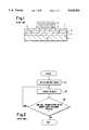
- FIG. 1is a sectional view schematically showing the structure of a typical memory cell transistor provided in a flash memory
- FIG. 2is a flowchart representing the sequence of an erase processing executed in a prior art flash memory
- FIG. 3is a flowchart representing the sequence of a write processing executed in a prior art flash memory
- FIG. 4is a block diagram illustrating the entire constitution of the non-volatile semiconductor memory device according to a first embodiment of the present invention
- FIG. 5is a circuit diagram illustrating the constitution of a minimal block portion in the memory cell array shown in FIG. 4;
- FIG. 6is a diagram showing the relationship between potentials of each signal line in the circuit shown in FIG. 5;
- FIG. 7is a graph showing a change of the threshold level relative to time in the erase operation
- FIG. 8is a graph showing a change of the threshold level relative to time in the write operation
- FIG. 9is a flowchart representing the sequence of an erase processing executed in the first embodiment
- FIG. 10is a flowchart representing the sequence of a write processing executed in the first embodiment
- FIG. 11is a block diagram illustrating the entire constitution of the non-volatile semiconductor memory device according to a second embodiment of the present invention.
- FIG. 12is a circuit diagram illustrating the constitution of a minimal block portion in the regular memory cell array and a portion in the verify/monitor memory cell array shown in FIG. 11.
- FIG. 1schematically shows the structure of a memory cell transistor provided in a flash memory.
- reference 1denotes an N-type silicon substrate; reference 2 a P-type well formed on the substrate 1; reference 3 an N-type diffusion layer constituting a drain (region); reference 4 an N-type diffusion layer constituting a source (region); reference 5 a control gate; reference 6 a floating gate; and reference 7 an insulation layer.
- writingmeans a processing of injecting electrons into the floating gate 6 of the memory cell transistor and, in a read operation, bringing the memory cell transistor to an OFF state.
- Such a stateis reckoned as, for example, a "0" stored state.
- erasuremeans a processing of drawing out electrons injected into the floating gate 6 of the memory cell transistor and, in a read operation, bringing the memory cell transistor to an ON state. Such a state is reckoned as, for example, a "1" stored state.
- a write processinghas been carried out, for example, by selecting potentials of the control gate 5, the source 4, and the drain 3, to be 12 V, 0 V, and 5 V, respectively; causing an avalanche breakdown phenomenon in the vicinity of the drain 3 to thereby generate electrons (i.e., hot carriers); and injecting the generated electrons into the floating gate 6.
- an erase processinghas been carried out, for example, by selecting potentials of the control gate 5 and the source 4, to be 5 V and 12 V, respectively; bringing the drain 3 to an open state; and utilizing a tunnel effect to thereby draw out electrons injected into the floating gate 6, toward the source 4.
- Such a processingis generally referred to as a "source" erasure.
- Another erase processinghas been carried out by selecting potentials of the control gate 5 and the P-type well 2, to be 0 V and 12 V, respectively; bringing the source 4 and the drain 3 to an open state, respectively; and utilizing a tunnel effect to thereby draw out electrons injected into the floating gate 6, toward the P-type well 2.
- Such a processingis generally referred to as a "channel" erasure.
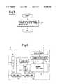
- a writingis first carried out with respect to all of memory cell transistors included in a block which is an object of erasure ("WRITE BEFORE ERASE” processing at step S1), and an erasure is then carried out with respect to all of the memory cell transistors in the object block ("ERASE EN BLOC" processing at step S2).
- ERASE EN BLOCthe manner of erasing en bloc is referred to as "flash erasure", for convenience.
- flash erasurethe manner of erasing en bloc.
- a judgment whether memory cell transistors with insufficient erasure are present (YES) or not (NO)is carried out. Where the judgment indicates YES, the control returns to step S2, and where the judgment indicates NO, the control comes to an END.
- a verify processingis carried out, one bit by bit, with respect to all of the memory cell transistors in the object block.
- a flash erasure operationis repeated until the erasure is completed with respect to all of the memory cell transistors in the object block.
- the verify processingis carried out after the flash erasure.
- the verify processingmust be carried out, one bit by bit, with respect to all of the memory cell transistors, and thus requires a great deal of time.
- the prior art flash memoryhas required the writing into all of the memory cell transistors in the object block of flash erasure before the flash erasure, and has required the bit-by-bit verify processing after the flash erasure. Accordingly, a problem has been posed in that it is impossible to carry out an erase operation and write operation with high speed.
- FIG. 4illustrates the entire constitution of the non-volatile semiconductor memory device according to a first embodiment of the present invention.
- reference 8denotes a chip constituting the present device
- reference 9denotes a regular memory cell array in which a plurality of memory cell transistors (flash memory cell transistors) are arranged in matrix.
- reference 10denotes an address buffer for effecting a buffering of a block address signal, a row address signal and a column address signal, respectively, fed from the outside of the chip 8; and reference 11 denotes a block decoder for decoding an internal block address signal output from the address buffer 10 and thereby selecting a block.
- reference 12denotes a row decoder for decoding an internal row address signal output from the address buffer 10 and thereby selecting a word line
- reference 13denotes a circuit including a column decoder for decoding an internal column address signal output from the address buffer 10 and thereby selecting a column line, a sense amplifier (S/A) used in a read operation, and a write amplifier (W/A) used in a write operation.
- S/Asense amplifier
- W/Awrite amplifier
- reference 14denotes a data input/output (I/O) buffer for effecting a buffering of read data and write data
- reference 15denotes a write/erase (W/E) control circuit for controlling a writing and erasure of data
- reference 16denotes a source control circuit for controlling electrical states of respective sources of each memory cell transistor.
- FIG. 5illustrates the circuit constitution of a minimal block portion in the memory cell array 9 shown in FIG. 4.
- references 17 11 to 17 22denote memory cell transistors, each formed in a P-type well (see FIG. 1); references WL1 and WL2 denote word lines; references BL1 and BL2 denote bit lines; references 18 1 and 18 2 denote N-channel MOS transistors, each constituting a select gate; reference SG1 denotes a select signal for controlling ON/OFF of the transistors 18 1 and 18 2 ; reference SL denotes a common source line for the memory cell transistors 17 11 to 17 22 ; references 19 1 and 19 2 denote N-channel MOS transistors, each constituting a select gate; and reference SG2 denotes a select signal for controlling ON/OFF of the transistors 19 1 and 19 2 .
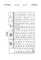
- FIG. 6shows the relationship between potentials of each signal line in the circuit shown in FIG. 5. Namely, it shows voltages applied to the word lines WL1, WL2, the select signal SG1, the bit lines BL1, BL2, the select signal SG2, the common source line SL, and the P-type well, when the circuit block shown in FIG. 5 is selected, or not selected, in the cases where a channel erasure, source erasure, writing, and verify after writing, are carried out.
- the device according to the first embodimentis constituted such that the voltages shown in FIG. 6 are applied to the word lines WL1, WL2, the select signal SG1, the bit lines BL1, BL2, the select signal SG2, the common source line SL, and the P-type well, respectively, to thereby carry out the channel erasure, the source erasure, the writing, and the verify after writing.
- the potentials of the word lines WL1 and WL2are set to be -10 V, respectively.
- the potential of the select signal SG1is set to be 0 V, and thus the transistors 18 1 and 18 2 are turned OFF.
- each drain of the memory cell transistors 17 11 to 17 22is brought to an open state.
- the potential of the select signal SG2is set to be 5 V, and thus the transistors 19 1 and 19 2 are turned ON and the potential of the common source line SL is set to be 5 V.
- each source of the memory cell transistors 17 11 to 17 22is set to be 5 V.
- the potential of the P-type wellis set to be 0 V.
- a curve indicated by reference 21is obtained in the case where "0" data has been written into a memory cell transistor before erasure, and thus the threshold level of the memory cell transistor has been set to be relatively high. Also, a curve indicated by reference 22 is obtained in the case where "1" data has been written into a memory cell transistor before erasure, and thus the threshold level of the memory cell transistor has been set to be relatively low.
- the potentials of the word lines WL1 and WL2are set to be -10 V, respectively.
- the potentials of the select signals SG1 and SG2are set to be 0 V, respectively, and thus each drain and each source of the memory cell transistors 17 11 to 17 22 are brought to an open state.
- the potential of the P-type wellis set to be 5 V.
- the potentials of the word lines WL1 and WL2are set to be 0 V, respectively. Also, the potentials of the select signals SG1 and SG2 are set to be 0 V, respectively, and thus the transistors 18 1 , 18 2 , 19 1 and 19 2 are turned OFF. As a result, each drain and each source of the memory cell transistors 17 11 to 17 22 are brought to an open state.
- the potentials of the word lines WL1 and WL2are set to be 0 to 5 V, respectively. Also, the potentials of the select signals SG1 and SG2 are set to be 0 V, respectively, and thus the transistors 18 1 , 18 2 , 19 1 and 19 2 are turned OFF. As a result, each drain and each source of the memory cell transistors 17 11 to 17 22 are brought to an open state.
- the potential of the word line WL1is set to be 20 V and the potential of the word line WL2 is set to be 0 to 10 V.
- the potential of the select signal SG1is set to be 5 V, and thus the transistors 18 1 and 18 2 are turned ON.
- the potentials of the bit lines BL1 and BL2are set to be 5 V and 0 V, respectively, and thus the potentials of each drain of the memory cell transistors 17 11 and 17 12 are brought to 5 V and 0 V, respectively.
- the potential of the select signal SG2is set to be 0 V, and thus the transistors 19 1 and 19 2 are turned OFF. As a result, each source of the memory cell transistors 17 11 and 17 12 is brought to an open state.
- the potential of the P-type wellis set to be 0 V.
- the threshold level (Vth) of the memory cell transistor 17 11is changed, as shown by a curve indicated by reference 23 in FIG. 8.
- the threshold level (Vth) of the memory cell transistor 17 11is changed, as shown by a curve indicated by reference 24 in FIG. 8.
- the threshold level of the memory cell transistor 17 11is settled to the state in which "1" is sufficiently written into the memory cell transistor 17 11
- the threshold level of the memory cell transistor 17 12is settled to the state in which "0" is sufficiently written into the memory cell transistor 17 12 .
- the threshold level of the memory cell transistor 17 12is raised up to above 5.5 V. Accordingly, with respect to the memory cell transistor 17 12 into which "0" is to be written, it becomes unnecessary to carry out the verify after writing. Namely, only with respect to the memory cell transistor 17 11 into which "1" is to be written, one has only to carry out the verify after writing.
- a writingcan be carried out by executing an erase processing sequence shown in FIG. 9 and executing a write processing sequence shown in FIG. 10.
- a flash erasureis carried out with respect to all of memory cell transistors included in a block which is an object of erasure (e.g., the circuit block shown in FIG. 5), and thus all of the memory cell transistors are brought to an overerased state ("ERASE EN BLOC (OVERERASE)" processing at step S10).
- ERASE EN BLOCOVERERASE
- a writing of "0" or “1”is carried out simultaneously, with units of a plurality of memory cell transistors connected to an identical word line in the object block of erasure (see step S21).
- a judgment whether memory cell transistors with insufficient writing of "1" are present (YES) or not (NO)is carried out. Where the judgment indicates YES, the control returns to step S21, and where the judgment indicates NO, the control comes to an END. Namely, the writing is repeated while the verify operation is carried out only with respect to memory cell transistors into which "1" is written.
- the writingis carried out simultaneously, with units of a predetermined plurality of memory cell transistors. Furthermore, only with respect to memory cell transistors of which each threshold level should be selected to be low (in the example, the memory cell transistor 17 11 into which "1" is to be written), one has only to carry out the verify processing.
- the first embodimentit is possible to realize the erase and write operation with a higher speed than in the prior art flash memory.
- FIG. 11illustrates the entire constitution of the non-volatile semiconductor memory device according to a second embodiment of the present invention.
- the devicefurther includes a verify/monitor memory cell array 25 provided for verification and monitoring of the regular memory cell transistors included in the memory cell array 9, and a circuit 26 with a function equivalent to that of the circuit 13 (column decoder, sense amplifier (S/A), and write amplifier (W/A)).
- a verify/monitor memory cell array 25provided for verification and monitoring of the regular memory cell transistors included in the memory cell array 9, and a circuit 26 with a function equivalent to that of the circuit 13 (column decoder, sense amplifier (S/A), and write amplifier (W/A)).
- FIG. 12illustrates the circuit constitution of a minimal block portion in the regular memory cell array 9 and a portion in the verify/monitor memory cell array 25 shown in FIG. 11.
- reference 27denotes a predetermined minimal block portion in the memory cell array 9
- reference 28denotes a corresponding portion in the verify/monitor memory cell array 25, provided for the block portion 27.
- references 29 1denotes a verify/monitor memory cell transistor provided for the regular memory cell transistors 17 11 and 17 12
- references 29 2denotes a verify/monitor memory cell transistor provided for the regular memory cell transistors 17 21 and 17 22 .
- the verify/monitor memory cell transistors 29 1 and 29 2are formed in a P-type well (see FIG. 1) in the same manner as the memory cell transistors 17 11 to 17 22 .
- references MBL1 and MBL2denote verify/monitor bit lines
- references 30 1 , 30 2 , 31 1 and 31 2denote N-channel MOS transistors, each constituting a verify/monitor select gate.
- the potential of the word line WL1is set to be 20 V and the potential of the word line WL2 is set to be 0 to 10 V. Accordingly, by setting the potential of the bit line MBL1 to be 5 V and setting the potential of the bit line MBL2 to be 0 to 5 V, it is possible to write "1" into the verify/monitor memory cell transistor 29 1 .
- the potential of the word line WL1is set to be 0 to 10 V and the potential of the word line WL2 is set to be 20 V.
- the potential of the bit line MBL1is set to be 0 to 5 V and setting the potential of the bit line MBL2 to be 5 V, it is possible to write "1" into the verify/monitor memory cell transistor 29 2 .
- the verify after writingcan be carried out using the verify/monitor memory cell transistors 29 1 and 29 2 .
- the regular memory cell transistors 17 11 to 17 22it becomes unnecessary to carry out the verify after writing.
- the second embodimentit is possible to realize the erase and write operation with a higher speed than in the first embodiment.
- each of the verify/monitor memory cell transistors 29 1 , 29 2is provided to have its own bit line MBL1, MBL2, independently of the regular bit lines BL1 and BL2.
- the writing into memory cell transistorsis carried out by injecting electrons based on the tunnel current from the drain region into the floating gate
- the writingmay be carried out by injecting electrons based on the tunnel current from the source region into the floating gate, from the drain and source regions into the floating gate, or from the well region into the floating gate, or may be carried out by injecting electrons generated based on an avalanche breakdown phenomenon in the vicinity of the drain region, into the floating gate.
Landscapes
- Read Only Memory (AREA)
- Semiconductor Memories (AREA)
Abstract
Description
Claims (6)
Applications Claiming Priority (2)
| Application Number | Priority Date | Filing Date | Title |
|---|---|---|---|
| JP5985793AJPH06275087A (en) | 1993-03-19 | 1993-03-19 | Nonvolatile semiconductor memory device |
| JP5-059857 | 1993-03-19 |
Publications (1)
| Publication Number | Publication Date |
|---|---|
| US5438544Atrue US5438544A (en) | 1995-08-01 |
Family
ID=13125276
Family Applications (1)
| Application Number | Title | Priority Date | Filing Date |
|---|---|---|---|
| US08/187,541Expired - LifetimeUS5438544A (en) | 1993-03-19 | 1994-01-28 | Non-volatile semiconductor memory device with function of bringing memory cell transistors to overerased state, and method of writing data in the device |
Country Status (3)
| Country | Link |
|---|---|
| US (1) | US5438544A (en) |
| JP (1) | JPH06275087A (en) |
| KR (1) | KR970003095B1 (en) |
Cited By (32)
| Publication number | Priority date | Publication date | Assignee | Title |
|---|---|---|---|---|
| US5568419A (en)* | 1994-07-28 | 1996-10-22 | Kabushiki Kaisha Toshiba | Non-volatile semiconductor memory device and data erasing method therefor |
| WO1997019452A1 (en)* | 1995-11-17 | 1997-05-29 | Macronix International Co., Ltd. | Method and system for soft programming algorithm |
| US5740104A (en)* | 1997-01-29 | 1998-04-14 | Micron Technology, Inc. | Multi-state flash memory cell and method for programming single electron differences |
| US5745410A (en)* | 1995-11-17 | 1998-04-28 | Macronix International Co., Ltd. | Method and system for soft programming algorithm |
| US5748538A (en)* | 1996-06-17 | 1998-05-05 | Aplus Integrated Circuits, Inc. | OR-plane memory cell array for flash memory with bit-based write capability, and methods for programming and erasing the memory cell array |
| US5754477A (en)* | 1997-01-29 | 1998-05-19 | Micron Technology, Inc. | Differential flash memory cell and method for programming |
| US5801401A (en)* | 1997-01-29 | 1998-09-01 | Micron Technology, Inc. | Flash memory with microcrystalline silicon carbide film floating gate |
| US5852306A (en)* | 1997-01-29 | 1998-12-22 | Micron Technology, Inc. | Flash memory with nanocrystalline silicon film floating gate |
| US5926740A (en)* | 1997-10-27 | 1999-07-20 | Micron Technology, Inc. | Graded anti-reflective coating for IC lithography |
| US6140181A (en)* | 1997-11-13 | 2000-10-31 | Micron Technology, Inc. | Memory using insulator traps |
| US6309907B1 (en) | 1997-07-29 | 2001-10-30 | Micron Technology, Inc. | Method of fabricating transistor with silicon oxycarbide gate |
| US20020126536A1 (en)* | 1997-07-29 | 2002-09-12 | Micron Technology, Inc. | Deaprom and transistor with gallium nitride or gallium aluminum nitride gate |
| US6452837B2 (en)* | 1999-12-27 | 2002-09-17 | Kabushiki Kaisha Toshiba | Nonvolatile semiconductor memory and threshold voltage control method therefor |
| US6492694B2 (en) | 1998-02-27 | 2002-12-10 | Micron Technology, Inc. | Highly conductive composite polysilicon gate for CMOS integrated circuits |
| US6504224B1 (en) | 1998-02-25 | 2003-01-07 | Micron Technology, Inc. | Methods and structures for metal interconnections in integrated circuits |
| US6541859B1 (en) | 1998-02-25 | 2003-04-01 | Micron Technology, Inc. | Methods and structures for silver interconnections in integrated circuits |
| US20030235079A1 (en)* | 2002-06-21 | 2003-12-25 | Micron Technology, Inc. | Nor flash memory cell with high storage density |
| US20030235081A1 (en)* | 2002-06-21 | 2003-12-25 | Micron Technology, Inc. | Nanocrystal write once read only memory for archival storage |
| US20040004247A1 (en)* | 2002-07-08 | 2004-01-08 | Micron Technology, Inc. | Memory utilizing oxide-nitride nanolaminates |
| US20040004245A1 (en)* | 2002-07-08 | 2004-01-08 | Micron Technology, Inc. | Memory utilizing oxide-conductor nanolaminates |
| US6746893B1 (en) | 1997-07-29 | 2004-06-08 | Micron Technology, Inc. | Transistor with variable electron affinity gate and methods of fabrication and use |
| US20040130951A1 (en)* | 2002-06-21 | 2004-07-08 | Micron Technology, Inc. | Write once read only memory employing charge trapping in insulators |
| US20040164341A1 (en)* | 1997-07-29 | 2004-08-26 | Micron Technology, Inc. | Operating a memory device |
| US6794255B1 (en) | 1997-07-29 | 2004-09-21 | Micron Technology, Inc. | Carburized silicon gate insulators for integrated circuits |
| US6835638B1 (en) | 1997-07-29 | 2004-12-28 | Micron Technology, Inc. | Silicon carbide gate transistor and fabrication process |
| US6965123B1 (en) | 1997-07-29 | 2005-11-15 | Micron Technology, Inc. | Transistor with variable electron affinity gate and methods of fabrication and use |
| US20060024878A1 (en)* | 1997-07-29 | 2006-02-02 | Micron Technology, Inc. | Deaprom having amorphous silicon carbide gate insulator |
| US7130220B2 (en) | 2002-06-21 | 2006-10-31 | Micron Technology, Inc. | Write once read only memory employing floating gates |
| US7166509B2 (en) | 2002-06-21 | 2007-01-23 | Micron Technology, Inc. | Write once read only memory with large work function floating gates |
| US7221586B2 (en) | 2002-07-08 | 2007-05-22 | Micron Technology, Inc. | Memory utilizing oxide nanolaminates |
| US7709402B2 (en) | 2006-02-16 | 2010-05-04 | Micron Technology, Inc. | Conductive layers for hafnium silicon oxynitride films |
| US8501563B2 (en) | 2005-07-20 | 2013-08-06 | Micron Technology, Inc. | Devices with nanocrystals and methods of formation |
Families Citing this family (1)
| Publication number | Priority date | Publication date | Assignee | Title |
|---|---|---|---|---|
| JP2004145910A (en) | 2002-10-21 | 2004-05-20 | Renesas Technology Corp | Nonvolatile semiconductor storage device |
Citations (2)
| Publication number | Priority date | Publication date | Assignee | Title |
|---|---|---|---|---|
| US5270979A (en)* | 1991-03-15 | 1993-12-14 | Sundisk Corporation | Method for optimum erasing of EEPROM |
| US5295107A (en)* | 1992-03-02 | 1994-03-15 | Nec Corporation | Method of erasing data stored in flash type nonvolatile memory cell |
- 1993
- 1993-03-19JPJP5985793Apatent/JPH06275087A/ennot_activeWithdrawn
- 1994
- 1994-01-28USUS08/187,541patent/US5438544A/ennot_activeExpired - Lifetime
- 1994-01-31KRKR1019940001686Apatent/KR970003095B1/ennot_activeExpired - Fee Related
Patent Citations (2)
| Publication number | Priority date | Publication date | Assignee | Title |
|---|---|---|---|---|
| US5270979A (en)* | 1991-03-15 | 1993-12-14 | Sundisk Corporation | Method for optimum erasing of EEPROM |
| US5295107A (en)* | 1992-03-02 | 1994-03-15 | Nec Corporation | Method of erasing data stored in flash type nonvolatile memory cell |
Non-Patent Citations (2)
| Title |
|---|
| IEEE Journal of Solid State Circuits, vol. 24, No. 5, Oct. 198, pp. 1259 1264 A 90 ns One Million Erase/Program Cycle 1 Mbit Flash Memory .* |
| IEEE Journal of Solid-State Circuits, vol. 24, No. 5, Oct. 198, pp. 1259-1264 "A 90-ns One-Million Erase/Program Cycle 1-Mbit Flash Memory". |
Cited By (99)
| Publication number | Priority date | Publication date | Assignee | Title |
|---|---|---|---|---|
| US5568419A (en)* | 1994-07-28 | 1996-10-22 | Kabushiki Kaisha Toshiba | Non-volatile semiconductor memory device and data erasing method therefor |
| WO1997019452A1 (en)* | 1995-11-17 | 1997-05-29 | Macronix International Co., Ltd. | Method and system for soft programming algorithm |
| US5745410A (en)* | 1995-11-17 | 1998-04-28 | Macronix International Co., Ltd. | Method and system for soft programming algorithm |
| US5748538A (en)* | 1996-06-17 | 1998-05-05 | Aplus Integrated Circuits, Inc. | OR-plane memory cell array for flash memory with bit-based write capability, and methods for programming and erasing the memory cell array |
| US5989958A (en)* | 1997-01-29 | 1999-11-23 | Micron Technology, Inc. | Flash memory with microcrystalline silicon carbide film floating gate |
| US7110299B2 (en) | 1997-01-29 | 2006-09-19 | Micron Technology, Inc. | Transistor with nanocrystalline silicon gate structure |
| US5801401A (en)* | 1997-01-29 | 1998-09-01 | Micron Technology, Inc. | Flash memory with microcrystalline silicon carbide film floating gate |
| US5852306A (en)* | 1997-01-29 | 1998-12-22 | Micron Technology, Inc. | Flash memory with nanocrystalline silicon film floating gate |
| US20050146938A1 (en)* | 1997-01-29 | 2005-07-07 | Micron Technology, Inc. | Transistor with nanocrystalline silicon gate structure |
| US5959896A (en)* | 1997-01-29 | 1999-09-28 | Micron Technology Inc. | Multi-state flash memory cell and method for programming single electron differences |
| US6912158B2 (en) | 1997-01-29 | 2005-06-28 | Micron Technology, Inc. | Transistor with nanocrystalline silicon gate structure |
| US6009018A (en)* | 1997-01-29 | 1999-12-28 | Micron Technology, Inc. | Differential flash memory cell and method for programming same |
| US6141256A (en)* | 1997-01-29 | 2000-10-31 | Micron Technology, Inc. | Differential flash memory cell and method for programming same |
| US5754477A (en)* | 1997-01-29 | 1998-05-19 | Micron Technology, Inc. | Differential flash memory cell and method for programming |
| US6166401A (en)* | 1997-01-29 | 2000-12-26 | Micron Technology, Inc. | Flash memory with microcrystalline silicon carbide film floating gate |
| US20060273375A1 (en)* | 1997-01-29 | 2006-12-07 | Micron Technology, Inc. | Transistor with nanocrystalline silicon gate structure |
| US20030206445A1 (en)* | 1997-01-29 | 2003-11-06 | Micron Technology, Inc. | Flash memory with nanocrystalline silicon film floating gate |
| US6300193B1 (en) | 1997-01-29 | 2001-10-09 | Micron Technology, Inc. | Flash memory with nanocrystalline silicon film floating gate |
| US6574144B2 (en) | 1997-01-29 | 2003-06-03 | Micron Technology, Inc. | Flash memory with nanocrystalline silicon film coating gate |
| US5740104A (en)* | 1997-01-29 | 1998-04-14 | Micron Technology, Inc. | Multi-state flash memory cell and method for programming single electron differences |
| US6407424B2 (en) | 1997-01-29 | 2002-06-18 | Micron Technology, Inc. | Flash memory with nanocrystalline silicon film floating gate |
| US7242049B2 (en) | 1997-07-29 | 2007-07-10 | Micron Technology, Inc. | Memory device |
| US6762068B1 (en) | 1997-07-29 | 2004-07-13 | Micron Technology, Inc. | Transistor with variable electron affinity gate and methods of fabrication and use |
| US7196929B1 (en) | 1997-07-29 | 2007-03-27 | Micron Technology Inc | Method for operating a memory device having an amorphous silicon carbide gate insulator |
| US7169666B2 (en) | 1997-07-29 | 2007-01-30 | Micron Technology, Inc. | Method of forming a device having a gate with a selected electron affinity |
| US6936849B1 (en) | 1997-07-29 | 2005-08-30 | Micron Technology, Inc. | Silicon carbide gate transistor |
| US6835638B1 (en) | 1997-07-29 | 2004-12-28 | Micron Technology, Inc. | Silicon carbide gate transistor and fabrication process |
| US6309907B1 (en) | 1997-07-29 | 2001-10-30 | Micron Technology, Inc. | Method of fabricating transistor with silicon oxycarbide gate |
| US7154153B1 (en) | 1997-07-29 | 2006-12-26 | Micron Technology, Inc. | Memory device |
| US6965123B1 (en) | 1997-07-29 | 2005-11-15 | Micron Technology, Inc. | Transistor with variable electron affinity gate and methods of fabrication and use |
| US6794255B1 (en) | 1997-07-29 | 2004-09-21 | Micron Technology, Inc. | Carburized silicon gate insulators for integrated circuits |
| US7141824B2 (en) | 1997-07-29 | 2006-11-28 | Micron Technology, Inc. | Transistor with variable electron affinity gate |
| US20040164341A1 (en)* | 1997-07-29 | 2004-08-26 | Micron Technology, Inc. | Operating a memory device |
| US7109548B2 (en) | 1997-07-29 | 2006-09-19 | Micron Technology, Inc. | Operating a memory device |
| US7005344B2 (en) | 1997-07-29 | 2006-02-28 | Micron Technology, Inc. | Method of forming a device with a gallium nitride or gallium aluminum nitride gate |
| US6746893B1 (en) | 1997-07-29 | 2004-06-08 | Micron Technology, Inc. | Transistor with variable electron affinity gate and methods of fabrication and use |
| US20060024878A1 (en)* | 1997-07-29 | 2006-02-02 | Micron Technology, Inc. | Deaprom having amorphous silicon carbide gate insulator |
| US20020126536A1 (en)* | 1997-07-29 | 2002-09-12 | Micron Technology, Inc. | Deaprom and transistor with gallium nitride or gallium aluminum nitride gate |
| US6781876B2 (en) | 1997-07-29 | 2004-08-24 | Micron Technology, Inc. | Memory device with gallium nitride or gallium aluminum nitride gate |
| US5926740A (en)* | 1997-10-27 | 1999-07-20 | Micron Technology, Inc. | Graded anti-reflective coating for IC lithography |
| US6140181A (en)* | 1997-11-13 | 2000-10-31 | Micron Technology, Inc. | Memory using insulator traps |
| US6232643B1 (en) | 1997-11-13 | 2001-05-15 | Micron Technology, Inc. | Memory using insulator traps |
| US6246606B1 (en) | 1997-11-13 | 2001-06-12 | Micron Technology, Inc. | Memory using insulator traps |
| US6545314B2 (en) | 1997-11-13 | 2003-04-08 | Micron Technology, Inc. | Memory using insulator traps |
| US6351411B2 (en) | 1997-11-13 | 2002-02-26 | Micron Technology, Inc. | Memory using insulator traps |
| US6541859B1 (en) | 1998-02-25 | 2003-04-01 | Micron Technology, Inc. | Methods and structures for silver interconnections in integrated circuits |
| US20030209775A1 (en)* | 1998-02-25 | 2003-11-13 | Micron Technology, Inc. | Methods and structures for metal interconnections in integrated circuits |
| US6879017B2 (en) | 1998-02-25 | 2005-04-12 | Micron Technology, Inc. | Methods and structures for metal interconnections in integrated circuits |
| US20050186773A1 (en)* | 1998-02-25 | 2005-08-25 | Micron Technology, Inc. | Methods and structures for metal interconnections in integrated circuits |
| US7186664B2 (en) | 1998-02-25 | 2007-03-06 | Micron Technology, Inc. | Methods and structures for metal interconnections in integrated circuits |
| US6504224B1 (en) | 1998-02-25 | 2003-01-07 | Micron Technology, Inc. | Methods and structures for metal interconnections in integrated circuits |
| US6492694B2 (en) | 1998-02-27 | 2002-12-10 | Micron Technology, Inc. | Highly conductive composite polysilicon gate for CMOS integrated circuits |
| US6573169B2 (en) | 1998-02-27 | 2003-06-03 | Micron Technology, Inc. | Highly conductive composite polysilicon gate for CMOS integrated circuits |
| US6452837B2 (en)* | 1999-12-27 | 2002-09-17 | Kabushiki Kaisha Toshiba | Nonvolatile semiconductor memory and threshold voltage control method therefor |
| US7112494B2 (en) | 2002-06-21 | 2006-09-26 | Micron Technology, Inc. | Write once read only memory employing charge trapping in insulators |
| US6888739B2 (en) | 2002-06-21 | 2005-05-03 | Micron Technology Inc. | Nanocrystal write once read only memory for archival storage |
| US6996009B2 (en) | 2002-06-21 | 2006-02-07 | Micron Technology, Inc. | NOR flash memory cell with high storage density |
| US8188533B2 (en) | 2002-06-21 | 2012-05-29 | Micron Technology, Inc. | Write once read only memory employing charge trapping in insulators |
| US20100067304A1 (en)* | 2002-06-21 | 2010-03-18 | Leonard Forbes | Write once read only memory employing charge trapping in insulators |
| US20030235081A1 (en)* | 2002-06-21 | 2003-12-25 | Micron Technology, Inc. | Nanocrystal write once read only memory for archival storage |
| US20050082599A1 (en)* | 2002-06-21 | 2005-04-21 | Micron Technology, Inc. | Nor flash memory cell with high storage density |
| US7113429B2 (en) | 2002-06-21 | 2006-09-26 | Micron Technology, Inc. | Nor flash memory cell with high storage density |
| US7130220B2 (en) | 2002-06-21 | 2006-10-31 | Micron Technology, Inc. | Write once read only memory employing floating gates |
| US7133315B2 (en) | 2002-06-21 | 2006-11-07 | Micron Technology, Inc. | Write once read only memory employing charge trapping in insulators |
| US7639528B2 (en) | 2002-06-21 | 2009-12-29 | Micron Technology, Inc. | Nanocrystal write once read only memory for archival storage |
| US7476586B2 (en) | 2002-06-21 | 2009-01-13 | Micron Technology, Inc. | NOR flash memory cell with high storage density |
| US20030235079A1 (en)* | 2002-06-21 | 2003-12-25 | Micron Technology, Inc. | Nor flash memory cell with high storage density |
| US7369435B2 (en) | 2002-06-21 | 2008-05-06 | Micron Technology, Inc. | Write once read only memory employing floating gates |
| US6804136B2 (en) | 2002-06-21 | 2004-10-12 | Micron Technology, Inc. | Write once read only memory employing charge trapping in insulators |
| US7154778B2 (en) | 2002-06-21 | 2006-12-26 | Micron Technology, Inc. | Nanocrystal write once read only memory for archival storage |
| US7166509B2 (en) | 2002-06-21 | 2007-01-23 | Micron Technology, Inc. | Write once read only memory with large work function floating gates |
| US20050199947A1 (en)* | 2002-06-21 | 2005-09-15 | Micron Technology, Inc. | Nanocrystal write once read only memory for archival storage |
| US7348237B2 (en) | 2002-06-21 | 2008-03-25 | Micron Technology, Inc. | NOR flash memory cell with high storage density |
| US7193893B2 (en) | 2002-06-21 | 2007-03-20 | Micron Technology, Inc. | Write once read only memory employing floating gates |
| US20050026375A1 (en)* | 2002-06-21 | 2005-02-03 | Micron Technology, Inc. | Write once read only memory employing charge trapping in insulators |
| US20080062757A1 (en)* | 2002-06-21 | 2008-03-13 | Micron Technology, Inc. | Nanocrystal write once read only memory for archival storage |
| US7257022B2 (en) | 2002-06-21 | 2007-08-14 | Micron Technology, Inc. | Nanocrystal write once read only memory for archival storage |
| US20040130951A1 (en)* | 2002-06-21 | 2004-07-08 | Micron Technology, Inc. | Write once read only memory employing charge trapping in insulators |
| US20040004247A1 (en)* | 2002-07-08 | 2004-01-08 | Micron Technology, Inc. | Memory utilizing oxide-nitride nanolaminates |
| US7687848B2 (en) | 2002-07-08 | 2010-03-30 | Micron Technology, Inc. | Memory utilizing oxide-conductor nanolaminates |
| US20050023574A1 (en)* | 2002-07-08 | 2005-02-03 | Micron Technology, Inc. | Memory utilizing oxide-nitride nanolaminates |
| US20060008966A1 (en)* | 2002-07-08 | 2006-01-12 | Micron Technology, Inc. | Memory utilizing oxide-conductor nanolaminates |
| US7433237B2 (en) | 2002-07-08 | 2008-10-07 | Micron Technology, Inc. | Memory utilizing oxide nanolaminates |
| US20060261376A1 (en)* | 2002-07-08 | 2006-11-23 | Micron Technology, Inc. | Memory utilizing oxide-nitride nanolaminates |
| US7489545B2 (en) | 2002-07-08 | 2009-02-10 | Micron Technology, Inc. | Memory utilizing oxide-nitride nanolaminates |
| US7494873B2 (en) | 2002-07-08 | 2009-02-24 | Micron Technology, Inc. | Memory utilizing oxide-nitride nanolaminates |
| US7583534B2 (en) | 2002-07-08 | 2009-09-01 | Micron Technolgy, Inc. | Memory utilizing oxide-conductor nanolaminates |
| US20060258097A1 (en)* | 2002-07-08 | 2006-11-16 | Micron Technology, Inc. | Memory utilizing oxide-nitride nanolaminates |
| US7221017B2 (en) | 2002-07-08 | 2007-05-22 | Micron Technology, Inc. | Memory utilizing oxide-conductor nanolaminates |
| US8228725B2 (en) | 2002-07-08 | 2012-07-24 | Micron Technology, Inc. | Memory utilizing oxide nanolaminates |
| US7221586B2 (en) | 2002-07-08 | 2007-05-22 | Micron Technology, Inc. | Memory utilizing oxide nanolaminates |
| US7728626B2 (en) | 2002-07-08 | 2010-06-01 | Micron Technology, Inc. | Memory utilizing oxide nanolaminates |
| US7847344B2 (en) | 2002-07-08 | 2010-12-07 | Micron Technology, Inc. | Memory utilizing oxide-nitride nanolaminates |
| US20040004245A1 (en)* | 2002-07-08 | 2004-01-08 | Micron Technology, Inc. | Memory utilizing oxide-conductor nanolaminates |
| US8501563B2 (en) | 2005-07-20 | 2013-08-06 | Micron Technology, Inc. | Devices with nanocrystals and methods of formation |
| US8921914B2 (en) | 2005-07-20 | 2014-12-30 | Micron Technology, Inc. | Devices with nanocrystals and methods of formation |
| US8067794B2 (en) | 2006-02-16 | 2011-11-29 | Micron Technology, Inc. | Conductive layers for hafnium silicon oxynitride films |
| US7709402B2 (en) | 2006-02-16 | 2010-05-04 | Micron Technology, Inc. | Conductive layers for hafnium silicon oxynitride films |
| US8785312B2 (en) | 2006-02-16 | 2014-07-22 | Micron Technology, Inc. | Conductive layers for hafnium silicon oxynitride |
Also Published As
| Publication number | Publication date |
|---|---|
| KR970003095B1 (en) | 1997-03-14 |
| KR940022566A (en) | 1994-10-21 |
| JPH06275087A (en) | 1994-09-30 |
Similar Documents
| Publication | Publication Date | Title |
|---|---|---|
| US5438544A (en) | Non-volatile semiconductor memory device with function of bringing memory cell transistors to overerased state, and method of writing data in the device | |
| US6818491B2 (en) | Set of three level concurrent word line bias conditions for a NOR type flash memory array | |
| US6567316B1 (en) | Nonvolatile semiconductor memory device and method of erasing data of nonvolatile semiconductor memory device | |
| US6160739A (en) | Non-volatile memories with improved endurance and extended lifetime | |
| JP3886673B2 (en) | Nonvolatile semiconductor memory device | |
| US7692969B2 (en) | Nonvolatile semiconductor memory device including plural memory cells and a dummy cell coupled to an end of a memory cell | |
| KR100331563B1 (en) | NAND-type flash memory device and method for operating the same | |
| US6205059B1 (en) | Method for erasing flash electrically erasable programmable read-only memory (EEPROM) | |
| US5973962A (en) | Method of programming non-volatile memory devices having a NAND type cell array | |
| US6515908B2 (en) | Nonvolatile semiconductor memory device having reduced erase time and method of erasing data of the same | |
| US5831905A (en) | Method for controlling erasure of nonvolatile semiconductor memory | |
| US5097444A (en) | Tunnel EEPROM with overerase protection | |
| US6856552B2 (en) | Semiconductor memory and method of driving the same | |
| US6947325B2 (en) | Non-volatile semiconductor memory device and controlling method of the same | |
| JP3895816B2 (en) | Nonvolatile semiconductor storage device and control method thereof, memory card, and storage system | |
| US6781882B2 (en) | Nonvolatile semiconductor storage device having a shortened time required for a data erasing operation and data erasing method thereof | |
| US5424991A (en) | Floating gate nonvolatile memory with uniformly erased threshold voltage | |
| US20030123296A1 (en) | Nonvolatile semiconductor memory device and data erase method therefor | |
| JP4698605B2 (en) | Semiconductor device and method for controlling semiconductor device | |
| EP1214715B1 (en) | 1 transistor cell for eeprom application | |
| JP2010086623A (en) | Nand type flash memory | |
| US7206241B2 (en) | Semiconductor device and programming method | |
| JP2735498B2 (en) | Non-volatile memory | |
| JP5422886B2 (en) | Semiconductor device | |
| US5831904A (en) | Non-volatile semiconductor memory device capable of conditioning over-erased memory cells |
Legal Events
| Date | Code | Title | Description |
|---|---|---|---|
| AS | Assignment | Owner name:FUJITSU LIMITED, JAPAN Free format text:ASSIGNMENT OF ASSIGNORS INTEREST;ASSIGNOR:MAKINO, TAKAMI;REEL/FRAME:006871/0747 Effective date:19940121 | |
| STCF | Information on status: patent grant | Free format text:PATENTED CASE | |
| FEPP | Fee payment procedure | Free format text:PAYOR NUMBER ASSIGNED (ORIGINAL EVENT CODE: ASPN); ENTITY STATUS OF PATENT OWNER: LARGE ENTITY | |
| FPAY | Fee payment | Year of fee payment:4 | |
| FPAY | Fee payment | Year of fee payment:8 | |
| FPAY | Fee payment | Year of fee payment:12 | |
| AS | Assignment | Owner name:FUJITSU MICROELECTRONICS LIMITED, JAPAN Free format text:ASSIGNMENT OF ASSIGNORS INTEREST;ASSIGNOR:FUJITSU LIMITED;REEL/FRAME:021998/0645 Effective date:20081104 Owner name:FUJITSU MICROELECTRONICS LIMITED,JAPAN Free format text:ASSIGNMENT OF ASSIGNORS INTEREST;ASSIGNOR:FUJITSU LIMITED;REEL/FRAME:021998/0645 Effective date:20081104 | |
| AS | Assignment | Owner name:FUJITSU SEMICONDUCTOR LIMITED, JAPAN Free format text:CHANGE OF NAME;ASSIGNOR:FUJITSU MICROELECTRONICS LIMITED;REEL/FRAME:024982/0245 Effective date:20100401 |