US5438477A - Die-attach technique for flip-chip style mounting of semiconductor dies - Google Patents
Die-attach technique for flip-chip style mounting of semiconductor diesDownload PDFInfo
- Publication number
- US5438477A US5438477AUS08/105,832US10583293AUS5438477AUS 5438477 AUS5438477 AUS 5438477AUS 10583293 AUS10583293 AUS 10583293AUS 5438477 AUS5438477 AUS 5438477A
- Authority
- US
- United States
- Prior art keywords
- die
- substrate
- expansion
- attach structure
- shape
- Prior art date
- Legal status (The legal status is an assumption and is not a legal conclusion. Google has not performed a legal analysis and makes no representation as to the accuracy of the status listed.)
- Expired - Lifetime
Links
Images

Classifications
- H—ELECTRICITY
- H01—ELECTRIC ELEMENTS
- H01L—SEMICONDUCTOR DEVICES NOT COVERED BY CLASS H10
- H01L24/00—Arrangements for connecting or disconnecting semiconductor or solid-state bodies; Methods or apparatus related thereto
- H01L24/80—Methods for connecting semiconductor or other solid state bodies using means for bonding being attached to, or being formed on, the surface to be connected
- H01L24/83—Methods for connecting semiconductor or other solid state bodies using means for bonding being attached to, or being formed on, the surface to be connected using a layer connector
- H—ELECTRICITY
- H01—ELECTRIC ELEMENTS
- H01L—SEMICONDUCTOR DEVICES NOT COVERED BY CLASS H10
- H01L24/00—Arrangements for connecting or disconnecting semiconductor or solid-state bodies; Methods or apparatus related thereto
- H01L24/01—Means for bonding being attached to, or being formed on, the surface to be connected, e.g. chip-to-package, die-attach, "first-level" interconnects; Manufacturing methods related thereto
- H01L24/26—Layer connectors, e.g. plate connectors, solder or adhesive layers; Manufacturing methods related thereto
- H01L24/28—Structure, shape, material or disposition of the layer connectors prior to the connecting process
- H01L24/29—Structure, shape, material or disposition of the layer connectors prior to the connecting process of an individual layer connector
- H—ELECTRICITY
- H01—ELECTRIC ELEMENTS
- H01L—SEMICONDUCTOR DEVICES NOT COVERED BY CLASS H10
- H01L24/00—Arrangements for connecting or disconnecting semiconductor or solid-state bodies; Methods or apparatus related thereto
- H01L24/80—Methods for connecting semiconductor or other solid state bodies using means for bonding being attached to, or being formed on, the surface to be connected
- H01L24/81—Methods for connecting semiconductor or other solid state bodies using means for bonding being attached to, or being formed on, the surface to be connected using a bump connector
- H—ELECTRICITY
- H01—ELECTRIC ELEMENTS
- H01L—SEMICONDUCTOR DEVICES NOT COVERED BY CLASS H10
- H01L2224/00—Indexing scheme for arrangements for connecting or disconnecting semiconductor or solid-state bodies and methods related thereto as covered by H01L24/00
- H01L2224/01—Means for bonding being attached to, or being formed on, the surface to be connected, e.g. chip-to-package, die-attach, "first-level" interconnects; Manufacturing methods related thereto
- H01L2224/26—Layer connectors, e.g. plate connectors, solder or adhesive layers; Manufacturing methods related thereto
- H01L2224/28—Structure, shape, material or disposition of the layer connectors prior to the connecting process
- H01L2224/29—Structure, shape, material or disposition of the layer connectors prior to the connecting process of an individual layer connector
- H01L2224/29001—Core members of the layer connector
- H01L2224/29099—Material
- H01L2224/291—Material with a principal constituent of the material being a metal or a metalloid, e.g. boron [B], silicon [Si], germanium [Ge], arsenic [As], antimony [Sb], tellurium [Te] and polonium [Po], and alloys thereof
- H01L2224/29101—Material with a principal constituent of the material being a metal or a metalloid, e.g. boron [B], silicon [Si], germanium [Ge], arsenic [As], antimony [Sb], tellurium [Te] and polonium [Po], and alloys thereof the principal constituent melting at a temperature of less than 400°C
- H—ELECTRICITY
- H01—ELECTRIC ELEMENTS
- H01L—SEMICONDUCTOR DEVICES NOT COVERED BY CLASS H10
- H01L2224/00—Indexing scheme for arrangements for connecting or disconnecting semiconductor or solid-state bodies and methods related thereto as covered by H01L24/00
- H01L2224/01—Means for bonding being attached to, or being formed on, the surface to be connected, e.g. chip-to-package, die-attach, "first-level" interconnects; Manufacturing methods related thereto
- H01L2224/26—Layer connectors, e.g. plate connectors, solder or adhesive layers; Manufacturing methods related thereto
- H01L2224/28—Structure, shape, material or disposition of the layer connectors prior to the connecting process
- H01L2224/29—Structure, shape, material or disposition of the layer connectors prior to the connecting process of an individual layer connector
- H01L2224/29001—Core members of the layer connector
- H01L2224/29099—Material
- H01L2224/2919—Material with a principal constituent of the material being a polymer, e.g. polyester, phenolic based polymer, epoxy
- H—ELECTRICITY
- H01—ELECTRIC ELEMENTS
- H01L—SEMICONDUCTOR DEVICES NOT COVERED BY CLASS H10
- H01L2224/00—Indexing scheme for arrangements for connecting or disconnecting semiconductor or solid-state bodies and methods related thereto as covered by H01L24/00
- H01L2224/01—Means for bonding being attached to, or being formed on, the surface to be connected, e.g. chip-to-package, die-attach, "first-level" interconnects; Manufacturing methods related thereto
- H01L2224/26—Layer connectors, e.g. plate connectors, solder or adhesive layers; Manufacturing methods related thereto
- H01L2224/28—Structure, shape, material or disposition of the layer connectors prior to the connecting process
- H01L2224/29—Structure, shape, material or disposition of the layer connectors prior to the connecting process of an individual layer connector
- H01L2224/29001—Core members of the layer connector
- H01L2224/29099—Material
- H01L2224/29198—Material with a principal constituent of the material being a combination of two or more materials in the form of a matrix with a filler, i.e. being a hybrid material, e.g. segmented structures, foams
- H01L2224/29298—Fillers
- H01L2224/29499—Shape or distribution of the fillers
- H—ELECTRICITY
- H01—ELECTRIC ELEMENTS
- H01L—SEMICONDUCTOR DEVICES NOT COVERED BY CLASS H10
- H01L2224/00—Indexing scheme for arrangements for connecting or disconnecting semiconductor or solid-state bodies and methods related thereto as covered by H01L24/00
- H01L2224/80—Methods for connecting semiconductor or other solid state bodies using means for bonding being attached to, or being formed on, the surface to be connected
- H01L2224/81—Methods for connecting semiconductor or other solid state bodies using means for bonding being attached to, or being formed on, the surface to be connected using a bump connector
- H01L2224/818—Bonding techniques
- H01L2224/81801—Soldering or alloying
- H—ELECTRICITY
- H01—ELECTRIC ELEMENTS
- H01L—SEMICONDUCTOR DEVICES NOT COVERED BY CLASS H10
- H01L2224/00—Indexing scheme for arrangements for connecting or disconnecting semiconductor or solid-state bodies and methods related thereto as covered by H01L24/00
- H01L2224/80—Methods for connecting semiconductor or other solid state bodies using means for bonding being attached to, or being formed on, the surface to be connected
- H01L2224/83—Methods for connecting semiconductor or other solid state bodies using means for bonding being attached to, or being formed on, the surface to be connected using a layer connector
- H01L2224/8319—Arrangement of the layer connectors prior to mounting
- H—ELECTRICITY
- H01—ELECTRIC ELEMENTS
- H01L—SEMICONDUCTOR DEVICES NOT COVERED BY CLASS H10
- H01L2224/00—Indexing scheme for arrangements for connecting or disconnecting semiconductor or solid-state bodies and methods related thereto as covered by H01L24/00
- H01L2224/80—Methods for connecting semiconductor or other solid state bodies using means for bonding being attached to, or being formed on, the surface to be connected
- H01L2224/83—Methods for connecting semiconductor or other solid state bodies using means for bonding being attached to, or being formed on, the surface to be connected using a layer connector
- H01L2224/838—Bonding techniques
- H01L2224/8385—Bonding techniques using a polymer adhesive, e.g. an adhesive based on silicone, epoxy, polyimide, polyester
- H—ELECTRICITY
- H01—ELECTRIC ELEMENTS
- H01L—SEMICONDUCTOR DEVICES NOT COVERED BY CLASS H10
- H01L2924/00—Indexing scheme for arrangements or methods for connecting or disconnecting semiconductor or solid-state bodies as covered by H01L24/00
- H01L2924/01—Chemical elements
- H01L2924/01005—Boron [B]
- H—ELECTRICITY
- H01—ELECTRIC ELEMENTS
- H01L—SEMICONDUCTOR DEVICES NOT COVERED BY CLASS H10
- H01L2924/00—Indexing scheme for arrangements or methods for connecting or disconnecting semiconductor or solid-state bodies as covered by H01L24/00
- H01L2924/01—Chemical elements
- H01L2924/01006—Carbon [C]
- H—ELECTRICITY
- H01—ELECTRIC ELEMENTS
- H01L—SEMICONDUCTOR DEVICES NOT COVERED BY CLASS H10
- H01L2924/00—Indexing scheme for arrangements or methods for connecting or disconnecting semiconductor or solid-state bodies as covered by H01L24/00
- H01L2924/01—Chemical elements
- H01L2924/01012—Magnesium [Mg]
- H—ELECTRICITY
- H01—ELECTRIC ELEMENTS
- H01L—SEMICONDUCTOR DEVICES NOT COVERED BY CLASS H10
- H01L2924/00—Indexing scheme for arrangements or methods for connecting or disconnecting semiconductor or solid-state bodies as covered by H01L24/00
- H01L2924/01—Chemical elements
- H01L2924/01013—Aluminum [Al]
- H—ELECTRICITY
- H01—ELECTRIC ELEMENTS
- H01L—SEMICONDUCTOR DEVICES NOT COVERED BY CLASS H10
- H01L2924/00—Indexing scheme for arrangements or methods for connecting or disconnecting semiconductor or solid-state bodies as covered by H01L24/00
- H01L2924/01—Chemical elements
- H01L2924/01015—Phosphorus [P]
- H—ELECTRICITY
- H01—ELECTRIC ELEMENTS
- H01L—SEMICONDUCTOR DEVICES NOT COVERED BY CLASS H10
- H01L2924/00—Indexing scheme for arrangements or methods for connecting or disconnecting semiconductor or solid-state bodies as covered by H01L24/00
- H01L2924/01—Chemical elements
- H01L2924/01029—Copper [Cu]
- H—ELECTRICITY
- H01—ELECTRIC ELEMENTS
- H01L—SEMICONDUCTOR DEVICES NOT COVERED BY CLASS H10
- H01L2924/00—Indexing scheme for arrangements or methods for connecting or disconnecting semiconductor or solid-state bodies as covered by H01L24/00
- H01L2924/01—Chemical elements
- H01L2924/01033—Arsenic [As]
- H—ELECTRICITY
- H01—ELECTRIC ELEMENTS
- H01L—SEMICONDUCTOR DEVICES NOT COVERED BY CLASS H10
- H01L2924/00—Indexing scheme for arrangements or methods for connecting or disconnecting semiconductor or solid-state bodies as covered by H01L24/00
- H01L2924/01—Chemical elements
- H01L2924/01075—Rhenium [Re]
- H—ELECTRICITY
- H01—ELECTRIC ELEMENTS
- H01L—SEMICONDUCTOR DEVICES NOT COVERED BY CLASS H10
- H01L2924/00—Indexing scheme for arrangements or methods for connecting or disconnecting semiconductor or solid-state bodies as covered by H01L24/00
- H01L2924/01—Chemical elements
- H01L2924/01079—Gold [Au]
- H—ELECTRICITY
- H01—ELECTRIC ELEMENTS
- H01L—SEMICONDUCTOR DEVICES NOT COVERED BY CLASS H10
- H01L2924/00—Indexing scheme for arrangements or methods for connecting or disconnecting semiconductor or solid-state bodies as covered by H01L24/00
- H01L2924/013—Alloys
- H01L2924/014—Solder alloys
- H—ELECTRICITY
- H01—ELECTRIC ELEMENTS
- H01L—SEMICONDUCTOR DEVICES NOT COVERED BY CLASS H10
- H01L2924/00—Indexing scheme for arrangements or methods for connecting or disconnecting semiconductor or solid-state bodies as covered by H01L24/00
- H01L2924/06—Polymers
- H01L2924/0665—Epoxy resin
- H—ELECTRICITY
- H01—ELECTRIC ELEMENTS
- H01L—SEMICONDUCTOR DEVICES NOT COVERED BY CLASS H10
- H01L2924/00—Indexing scheme for arrangements or methods for connecting or disconnecting semiconductor or solid-state bodies as covered by H01L24/00
- H01L2924/06—Polymers
- H01L2924/078—Adhesive characteristics other than chemical
- H01L2924/07802—Adhesive characteristics other than chemical not being an ohmic electrical conductor
- H—ELECTRICITY
- H01—ELECTRIC ELEMENTS
- H01L—SEMICONDUCTOR DEVICES NOT COVERED BY CLASS H10
- H01L2924/00—Indexing scheme for arrangements or methods for connecting or disconnecting semiconductor or solid-state bodies as covered by H01L24/00
- H01L2924/10—Details of semiconductor or other solid state devices to be connected
- H01L2924/102—Material of the semiconductor or solid state bodies
- H01L2924/1025—Semiconducting materials
- H01L2924/10251—Elemental semiconductors, i.e. Group IV
- H01L2924/10253—Silicon [Si]
- H—ELECTRICITY
- H01—ELECTRIC ELEMENTS
- H01L—SEMICONDUCTOR DEVICES NOT COVERED BY CLASS H10
- H01L2924/00—Indexing scheme for arrangements or methods for connecting or disconnecting semiconductor or solid-state bodies as covered by H01L24/00
- H01L2924/10—Details of semiconductor or other solid state devices to be connected
- H01L2924/11—Device type
- H01L2924/14—Integrated circuits
- H—ELECTRICITY
- H01—ELECTRIC ELEMENTS
- H01L—SEMICONDUCTOR DEVICES NOT COVERED BY CLASS H10
- H01L2924/00—Indexing scheme for arrangements or methods for connecting or disconnecting semiconductor or solid-state bodies as covered by H01L24/00
- H01L2924/30—Technical effects
- H01L2924/301—Electrical effects
- H01L2924/30105—Capacitance
- H—ELECTRICITY
- H01—ELECTRIC ELEMENTS
- H01L—SEMICONDUCTOR DEVICES NOT COVERED BY CLASS H10
- H01L2924/00—Indexing scheme for arrangements or methods for connecting or disconnecting semiconductor or solid-state bodies as covered by H01L24/00
- H01L2924/30—Technical effects
- H01L2924/35—Mechanical effects
- H01L2924/351—Thermal stress
- Y—GENERAL TAGGING OF NEW TECHNOLOGICAL DEVELOPMENTS; GENERAL TAGGING OF CROSS-SECTIONAL TECHNOLOGIES SPANNING OVER SEVERAL SECTIONS OF THE IPC; TECHNICAL SUBJECTS COVERED BY FORMER USPC CROSS-REFERENCE ART COLLECTIONS [XRACs] AND DIGESTS
- Y10—TECHNICAL SUBJECTS COVERED BY FORMER USPC
- Y10T—TECHNICAL SUBJECTS COVERED BY FORMER US CLASSIFICATION
- Y10T29/00—Metal working
- Y10T29/49—Method of mechanical manufacture
- Y10T29/4935—Heat exchanger or boiler making
Definitions
- the inventionrelates to techniques for mounting a semiconductor chip (die) or package to a substrate (another die, printed circuit board, or the like.
- a technique generally known as “flip chip” mountingis employed.
- a number of patentsshow that a semiconductor die (or “chip”) can be “flip-chip” mounted and connected to another die (or “substrate”) via a pattern or array of conductive bumps disposed on a surface of a semiconductor die, or on both the die and an underlying substrate.
- U.S. Pat. Nos. 4,825,284 and 4,926,241, incorporated by reference hereindescribe methods for "flip-chip” mounting of a semiconductor die to a substrate by means of conductive (solder) bumps.
- the conductive bumpsare ball-like structures formed of solder and disposed in a pattern on a surface of the die.
- a mating pattern of bond pads and/or similar conductive bumpsis disposed on a surface of the underlying substrate.
- the dieis positioned over the substrate and the conductive bumps on the die are "re-flowed" or otherwise fused to their counterpart connection elements on the surface of the substrate to form both electrical and mechanical connections between the die and the substrate.
- a bump-bonded assemblyincludes one or more relatively small silicon chips (or packages) mounted in face-to-face relationship to a larger silicon chip, package, or substrate. Solder balls are formed on the opposing faces of the chips (or packages) and the substrate, at a number of positions corresponding to one another. In other words, the pattern and spacing of the solder balls on the chip (or package) match the pattern and spacing of solder balls on the substrate.
- the conductive bumpsare arranged around a peripheral area of the die, although locating bumps in a central area of the die is also possible.
- the chip (or package)is brought into face-to-face relationship with the substrate, and with the solder balls of the chip (or package) aligned with the solder balls of the substrate.
- the chip (or package) and substrateare subjected to heat, which (ideally) causes the solder balls of the chip (or package) to fuse with the corresponding solder balls of the substrate, thereby forming solder joints between the chip and the substrate.
- the probability of mechanical shock-induced bump bond failuresaugments the overall problems associated with bump bonding, and makes conventional bump bonding techniques unsuitable for many harsh environments (e.g., many automotive, aircraft and military applications) without some auxiliary means of limiting mechanical shock.
- One possible approach to preventing mechanical shock-induced failures of bump bondsis to anchor the die firmly to the substrate in the process of forming bump bond connections, for example, via a die attach structure (e.g., a planar "spacer" between the die and substrate to which both are firmly attached).
- a die attach structuree.g., a planar "spacer" between the die and substrate to which both are firmly attached.
- commonly-owned U.S. Pat. No. 5,111,279discloses a preformed planar structure interposed between a chip and a substrate which is formed of materials which will tend to draw the chip towards the substrate. In this manner the die is secured and prevented from converting mechanical shock into shear forces at the bump bond connections.
- thermal coefficient mismatch with the die attach structurecan create additional thermally-induced stress problems.
- the die attach structure(interposed between the die and the substrate) is subjected to thermal changes, it may expand at a different rate in the vertical direction (i.e., in the die-to-substrate direction) than the bump bond connections (e.g., solder joints).
- the die attach structurecan create a situation where the bump bond connections are literally being pulled apart by the thermal expansion of the die attach structure.
- the diecan be cooled to reduce thermally induced stresses, both at the bump bond connections and within the die itself.
- Conductive cooling via heat-sink structurescan be used, but this approach tends to be bulky and expensive.
- Many active approaches to coolingare known in the art, including fan-forced gas (e.g., air) cooling whereby a flow of a cooling gas is directed at or around the die.
- a die attach structuredepending upon the material used, can provide some conductive cooling.
- a die attach structure interposed between the die and the substrateparticularly a planar structure interposed between the die and the substrate, tends to limit gas or fluid-based cooling in the die by preventing gas or fluid flow between the die and the substrate. This can be particularly troublesome in multi-tier stacked flip-chip assemblies where some dies may have very little exposed surface area.
- a die attach structuresuitable for interposition between a die (e.g., a semiconductor chip or package) and a substrate (e.g., another semiconductor chip or a printed circuit board), which mechanically joins the chip to the substrate without augmenting thermal stress problems of the assembled chip and substrate, and which facilitates cooling of the die.
- a diee.g., a semiconductor chip or package
- a substratee.g., another semiconductor chip or a printed circuit board
- a non-planar die attach structureis interposed between a die and a substrate.
- the die attach structureis suitably made of a thin sheet of material deformed in two or three dimensions to have a first set of peaks (positive excursions) on one side and a second set of peaks (negative excursions) on an opposite side.
- the die attach structureis rippled, having a "travelling-S" cross section. Vertical peaks extend longitudinally across the structure on both sides of the structure.
- the die attach structureis formed like an egg-crate, exhibiting arrays of peaks on both sides.
- the peaks on one side of the structureare attached (such as with an adhesive) to the die, and the peaks on the other side of the structure are attached to the substrate.
- the non-planar shape of the die attach structureprovides stress-relief for solder bump connections between the die and the substrate.
- the die attach structure of the present inventionis robust to the stresses associated with shock and preferably matches the coefficient of expansion of the solder bumps.
- the die attach structureis sized to fit within a central area of the die, so that the ball bump connections (e.g., solder joints) can be made outside the periphery of the die attach structure.
- the peaks on the one side of the die attach structureare coplanar, and the peaks on the opposite side of the die attach structure are also coplanar--the plane of the peaks of the opposite side being vertically offset from the plane of the one side.
- the die-attach structureis "rippled" or accordion-shaped (zig-zag folded), and is sized to fit between a die and a substrate (i.e., its area is made somewhat smaller than the outline of the die so that it fits inside of the bump bond connections (which are typically disposed just inside the periphery of the die), and its height is equal to the desired spacing between the die and substrate).
- the height of the die-attach structuredefines the ultimate height of solder joints formed between the die and the substrate.
- the die-attach structureis essentially a "sheet” of material formed in a "rippled” configuration similar to that of corrugated fiberglass or steel. Such rippled shapes are characterized by an overall planar volume, with a cross-section exhibiting a series of positive and negative peaks.
- the "rippled" shape of the die attach structurecan be a sinusoidal, or other curved "travelling-S" shape.
- the "rippled" shape of the die attachcan be a "triangular-wave” or “sawtooth” shape.
- channelsvoid areas extending in a longitudinal dimension
- positivee.g. top
- negativee.g., bottom
- gas or fluidcan be directed through these longitudinal channels to cool the die.
- the die-attach structureis assembled in a central area between a die and a substrate such that the die attaches to the top peaks of the die attach structure and the substrate attaches to the bottom peaks of the die attach structure (or vice-versa).
- Conductive bump contacts on the die and the substratemate outside of the central area of the die-attach structure, in a peripheral area of the die.
- the die-attach structureprotects the conductive bump contacts (bump bonds) from mechanical shock stress and substantially increases the magnitude of the shock required to damage the conductive bump contacts.
- the rippled shape of the die-attach structureexhibits desirable flexibility or "springiness", as compared with conventional (prior-art) planar structures and die attach techniques.
- TCEthermal coefficients of expansion
- the matching of the coefficient of expansion of the die-attach structure to the silicon die materialis accomplished by controlling the offset of the positive and negative peaks of the die-attach structure.
- a "die-attach" angle (“ ⁇ ")is defined by a line drawn between the positive and negative peaks of the die attach "rippled" shape, and another line drawn across the positive (or negative) peaks. (If the die attach is not angularly symmetrical, i.e., if the angles are different on opposite sides of an attach point, then the "steeper" die-attach angle dominates.) In this manner, the apparent vertical coefficient of expansion is effectively the TCE of die attach material times the die-attach angle ⁇ .
- This effectcan be used to minimize the mismatch in vertical coefficients of thermal expansion of the die-attach structure and the solder bumps, thereby providing for secure anchoring of the die and protection of the conductive bump contacts from mechanical shock without causing thermally-induced mechanical stresses (in the vertical direction) at the conductive bump contacts.
- a three-dimensional egg-crate shaped die attachcan be formed which has rows and columns of alternating positive and negative peaks. Open paths exist in egg-crate structures through which cooling gas or fluid can be directed. Whereas these paths were longitudinal, in the rippled die-attach structure, in the egg-crate shaped embodiment the paths will be more sinuous.
- thermal coefficient mismatchescan be accommodated in three dimensions.
- the egg-shape embodimentexhibits similar benefits as does the rippled embodiment of the die-attach structure.
- the inventive die-attach structurereinforces the flip-chipped assembly, and absorbs a significant portion of any mechanical shock applied to the assembly, thereby protecting the conductive bump contacts and reducing the probability of shock-induced failures of bump bond connections.
- the inventive die-attach techniquedoes not worsen thermal stresses within the assembly, and with proper selection of materials and shapes, can reduce thermally induced stresses.
- Chipsor paths through the “rippled” (or egg-crate) shape of the die attach permit cooling gas or fluid to be directed through the die-attach structure between the die and the substrate, permitting improved cooling of the die.
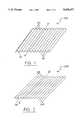
- FIG. 1is a perspective view of a "travelling-S" rippled die-attach structure, according to the invention.
- FIG. 2is a view of a "triangular” or “sawtooth” rippled die-attach structure, according to the invention.
- FIG. 3is a cross-sectional view of a semiconductor device assembly including a rippled die-attach structure, according to the invention.
- FIG. 4is a view of a die-attach structure with an egg-crate "texture", according to the invention.
- FIG. 1shows an example of a "rippled” or “travelling-S” die attach structure 100, sized to fit between a die and a substrate (i.e., its area is somewhat smaller than the outline of the die so that it fits inside of the bump bond connections, and its height is selected to establish a desired spacing between the die and the substrate).
- the die-attach structure 100is essentially a "sheet” of material formed (by any suitable means) to exhibit a “rippled” shape (cross-section).
- the "rippled" characteristic shapeis clearly seen at an edge 110 of the die-attach structure, where a sinusoidal "travelling-S" shape is evident.
- This "rippled" shape (or texture) of the die attach 100is a two-dimensional shape, i.e., it has a constant cross-section in one dimension, and is characterized by top peaks 120 and bottom peaks 130 offset from the top peaks.
- the top peaksare attached to a surface of a die with a suitable adhesive (such as epoxy), and the bottom peaks are attached to a surface of a substrate with a suitable adhesive (such as epoxy).
- a suitable adhesivesuch as epoxy
- the bottom peaksare attached to a surface of a substrate with a suitable adhesive (such as epoxy).
- the die-attach structureforms a mechanical joint between the die and the substrate.
- the die-attach structureis sized to be somewhat smaller than the smaller of the die and the substrate (typically the die is smaller than the substrate), in order that conductive bump contacts on the opposing faces of the die and substrate will form solder joints outside the periphery of the die-attach structure.
- the rippled cross-section of the die-attach structureresults in longitudinal "channels" being formed between the top peaks 120 and bottom peaks 130.
- One such channelis indicated generally along the line A--A' extending longitudinally across the die attach 100.
- FIG. 2shows an alternate embodiment 200 of a "rippled" die attach, similar to the travelling-S die attach 100 of FIG. 1, but having a two-dimensional triangular "sawtooth” shape rather than the sinusoidal (traveling-S) shape shown in FIG. 1.
- the die attach 200is sized to fit between a die and a substrate, and is essentially a "sheet” of attach material formed in a "rippled” sawtooth configuration. The triangular sawtooth shape is clearly seen at an edge 210 of the die attach.
- the shape of the die attach 200has top peaks 220 which attach to the die and bottom peaks 230 which attach to the substrate. "Channels" between the top peaks 220 and bottom peaks 230, such as the one indicated generally along the line B--B', extend across the die attach 200, through which gas or fluid can be directed through these channels to cool the die (once assembled).
- FIG. 3is a cross-sectional view of an assembly 300 wherein a die 320 is bump bonded to a substrate 310, using the die-attach structure 100 of FIG. 1. (The die-attach structure 200 of FIG. 2 could be substituted.)
- the die 320attaches to the top peaks 120 of the die-attach structure 100 by an adhesive 325 and the substrate 310 attaches to the bottom peaks 130 of the die attach 100 by an adhesive 326.
- Conductive bump contacts 330(one shown) electrically connect the die 320 to the substrate 310.
- the die-attach structure 100protects the conductive bump contacts 330 (bump bonds) from mechanical shock stress and substantially increases the magnitude of the shock required to damage the conductive bump contacts 330.
- the rippled shape of the die-attach structure 100will exhibit a certain degree of flexibility or "springiness", further alleviating the adverse effects of mechanical shock.
- the "rippled" shape of the die-attach structurecan exhibit beneficial thermal expansion behavior, especially in the vertical (as depicted in FIG. 3) direction, and the coefficient of expansion of the die-attach structure 100 can be tailored to match the coefficient of expansion of the conductive bump contacts 330, thereby reducing stresses caused by differences in vertical thermal expansion.
- a die-attach structure 100can be created that simultaneously matches the coefficient of expansion of the conductive bump contacts 330 (for example, solder) and reduces the effect of the coefficient of expansion mismatch between the die 320 and the substrate 310.
- the only requirement for selecting the material for the die-attach structure 100is that its temperature coefficient of expansion exceeds that of the crystal silicon material making up the die 320. This requirement is not difficult to meet, since most metals, including aluminum, copper, and magnesium, have temperature coefficients of expansion greater than crystal silicon.
- the apparent vertical coefficient of expansion of the die-attach structurecan be controlled by its rippled shape, and matched well to the coefficient of expansion of the die.
- a die-attach angle ⁇is defined as the angle formed by the intersection of a line drawn between a positive peak and the next vertically offset negative peak with a line drawn across the positive (or negative) peaks.
- TCEthermal coefficient of expansion
- the actual and apparent thermal coefficients of expansion for the die-attach structurecan be tailored to match the thermal coefficients of expansion of both the solder joints of the conductive bump contacts and the silicon die.
- the die-attach structureprovides for secure anchoring of the die to the substrate and provides protection from mechanical shock for the conductive bump contacts, without causing thermally-induced mechanical stresses (in the vertical direction) at the conductive bump contacts.
- a TCE mismatch between the substrate and the diecan cause thermally-induced stresses to occur which can crack the die or cause it to become detached from the substrate.
- the "rippled" shape of the die-attach structure of the present inventioncan be used to accommodate this mismatch in at least two different ways.
- the "rippled" shapehas a certain amount of flexibility in at least one dimension (horizontal, as depicted in FIGS. 1 and 2) and can absorb some of the thermal stress.
- similar thermal coefficient matching between the die and the substratecan be accomplished by controlling the angles between points of attachment of the die and substrate to the die attach, in a manner similar to that described above for matching vertical coefficients of expansion. By proper selection of both die attach material and die attach angle, both vertical and horizontal coefficients will be matched.
- cooling gas or fluidcan be directed between the die 320 and the substrate 310 through the channels (e.g., along line A--A', FIG. 1) to improve heat dissipation from the die.
- rippled, or two-dimensionally deformed shapes for a die-attach structureprovide flexibility in two dimensions (laterally and vertically), they do not provide "flexibility" in the longitudinal direction (i.e., along line A--A' of FIG. 1, or along line B--B' of FIG. 2). In order to achieve flexibility, and similar benefits thereof, in the longitudinal dimension, it is necessary to provide a three-dimension texture to the die-attach structure.
- FIG. 4shows a die-attach structure exhibiting deformations in three-dimensions.
- An example resembling an egg-crateis illustrated in FIG. 4.
- the egg-crate shapehas rows and columns of alternating positive peaks 420 and negative peaks 430. Further, open paths exist in the egg-crate structures (e.g., along line C--C') through which cooling gas or fluid can be directed.
- thermal coefficient mismatchescan be simultaneously accommodated in three dimensions (rather than only two, as was the case with the rippled shapes of FIGS. 1 and 2).
- the concepts discussed hereinabove with respect to rippled shapesare simply extended (to the longitudinal dimension) with the three-dimensionally deformed egg-crate (or similar) shape of the die-attach structure 400.
- the choice of whether to use the traveling "S" structure, the triangular structure or the fully developed egg crate structurewill be made depending upon the magnitude of the mismatch of TCE's of the substrate, conductive bump and die materials, and will vary from application to application.
Landscapes
- Engineering & Computer Science (AREA)
- Computer Hardware Design (AREA)
- Microelectronics & Electronic Packaging (AREA)
- Power Engineering (AREA)
- Wire Bonding (AREA)
Abstract
Description
The invention relates to techniques for mounting a semiconductor chip (die) or package to a substrate (another die, printed circuit board, or the like.
Semiconductor technology has shown a general trend towards dramatic increases in integrated circuit speed and density. Both of these trends are facilitated by an overall reduction in device (circuit element) geometries (sizes). As semiconductor circuit elements become smaller, the distances between them on a semiconductor die become smaller, and parasitics (such as parasitic capacitances) and switching currents become smaller. In technologies such as CMOS, where overall current draw and switching speed characteristics are dominated by the effects of parasitics, the result is a reduction in total power consumption at the same time as switching speed is improved. Overall speed is further improved by the reduction in signal propagation time between active devices (e.g., transistors) resulting from the shorter distances involved. Nevertheless, in high speed integrated circuitry based on sub-micron geometries, delays in the tens or hundreds of picoseconds can be appreciable.
In order to minimize the length of wiring between semiconductor devices, a technique generally known as "flip chip" mounting is employed. A number of patents show that a semiconductor die (or "chip") can be "flip-chip" mounted and connected to another die (or "substrate") via a pattern or array of conductive bumps disposed on a surface of a semiconductor die, or on both the die and an underlying substrate. For example U.S. Pat. Nos. 4,825,284 and 4,926,241, incorporated by reference herein, describe methods for "flip-chip" mounting of a semiconductor die to a substrate by means of conductive (solder) bumps. Typically, the conductive bumps are ball-like structures formed of solder and disposed in a pattern on a surface of the die. A mating pattern of bond pads and/or similar conductive bumps is disposed on a surface of the underlying substrate. The die is positioned over the substrate and the conductive bumps on the die are "re-flowed" or otherwise fused to their counterpart connection elements on the surface of the substrate to form both electrical and mechanical connections between the die and the substrate.
Similar techniques are known in the art for mounting a semiconductor device package to a printed circuit board or other substrate, although they tend to be on a larger scale than the techniques for mounting a semiconductor die to a substrate. U.S. Pat. Nos. 4,700,276, 5,006,673, and 5,077,633, incorporated by reference herein, are generally directed to such techniques. Semiconductor devices employing conductive bumps are commonly referred to as "pad array chip carriers", or as "bump grid arrays". Other references to pad array chip carriers and similar mounting techniques are found in "Pad Array Improves Density" (Electronic Packaging and Production, May 1992, p. 25.), "Overmolded Plastic Pad Array Carriers (OMPAC): A Low-Cost, High Interconnect Density IC Packaging Solution for Consumer and Industrial Electronics", (Freyman and Pennisi, IEEE Publication No. 0569-5503/91/0000-176, 1991), and "LED Array Modules by New Technology Microbump Bonding Method" (Hatada, Fujimoto, Ochi, Ishida, IEEE Transactions on Components, Hybrids and Manufacturing Technology, Vol. 13, No. 3, Sep. 1990, pp. 521-527). A related mounting scheme is disclosed in U.S. Pat. No. 4,717,066, incorporated herein by reference, wherein a gold alloy is used for the conductive bumps (balls) rather than solder.
Hereinafter, all conductive bump connection techniques, both for chips (semiconductor dies, e.g., "flip-chip" mounting) and packaged semiconductor devices (e.g., pad array chip carriers) will be referred to collectively as "bump bonding", and the resulting assembly of one element to another will be referred to as a "bump-bonded assembly".
Generally, as used herein, a bump-bonded assembly includes one or more relatively small silicon chips (or packages) mounted in face-to-face relationship to a larger silicon chip, package, or substrate. Solder balls are formed on the opposing faces of the chips (or packages) and the substrate, at a number of positions corresponding to one another. In other words, the pattern and spacing of the solder balls on the chip (or package) match the pattern and spacing of solder balls on the substrate. Generally, for bump bonding semiconductor dies, the conductive bumps are arranged around a peripheral area of the die, although locating bumps in a central area of the die is also possible. The chip (or package) is brought into face-to-face relationship with the substrate, and with the solder balls of the chip (or package) aligned with the solder balls of the substrate. The chip (or package) and substrate are subjected to heat, which (ideally) causes the solder balls of the chip (or package) to fuse with the corresponding solder balls of the substrate, thereby forming solder joints between the chip and the substrate.
When using bump bond technology, there are significant reliability issues associated with the bump breaking in use. It is widely known in the art that conductive bump connections between a die and a substrate may (and often will) break because of differences in rates of thermal expansion between the die and the substrate. Thermally induced mechanical stresses at the conductive bump bonds can build up to a point where the mechanical structure of the conductive bump fails and the bump breaks or is "torn" away from the die.
Although this failure mechanism is well documented, it is by no means the only failure mechanism. Stresses on conductive bumps caused by mechanical shock of moderate values (50-100 g's) can easily exceed the strength of the bump bond connections. In the absence of completely uniform distribution of stress over the array of solder bumps, individual conductive bumps can easily be broken, or torn away from the die, by stresses of this magnitude.
When added to the probability of thermally-induced bump bond failures, the probability of mechanical shock-induced bump bond failures augments the overall problems associated with bump bonding, and makes conventional bump bonding techniques unsuitable for many harsh environments (e.g., many automotive, aircraft and military applications) without some auxiliary means of limiting mechanical shock.
One possible approach to preventing mechanical shock-induced failures of bump bonds is to anchor the die firmly to the substrate in the process of forming bump bond connections, for example, via a die attach structure (e.g., a planar "spacer" between the die and substrate to which both are firmly attached). For example, commonly-owned U.S. Pat. No. 5,111,279, incorporated by reference herein, discloses a preformed planar structure interposed between a chip and a substrate which is formed of materials which will tend to draw the chip towards the substrate. In this manner the die is secured and prevented from converting mechanical shock into shear forces at the bump bond connections. Unfortunately, however, this may exacerbate the problem of alleviating thermally induced stresses within the die itself, and thermal mismatches between the die and the substrate. Since the die is now firmly mounted to the substrate (via the planar spacer), any stresses due to thermal coefficient mismatch are transmitted directly to the die, creating a risk of fracturing the die.
Further, thermal coefficient mismatch with the die attach structure can create additional thermally-induced stress problems. For example, as the die attach structure (interposed between the die and the substrate) is subjected to thermal changes, it may expand at a different rate in the vertical direction (i.e., in the die-to-substrate direction) than the bump bond connections (e.g., solder joints). As a result, the die attach structure can create a situation where the bump bond connections are literally being pulled apart by the thermal expansion of the die attach structure.
The die can be cooled to reduce thermally induced stresses, both at the bump bond connections and within the die itself. Conductive cooling via heat-sink structures can be used, but this approach tends to be bulky and expensive. Many active approaches to cooling are known in the art, including fan-forced gas (e.g., air) cooling whereby a flow of a cooling gas is directed at or around the die. A die attach structure, depending upon the material used, can provide some conductive cooling. However, a die attach structure interposed between the die and the substrate, particularly a planar structure interposed between the die and the substrate, tends to limit gas or fluid-based cooling in the die by preventing gas or fluid flow between the die and the substrate. This can be particularly troublesome in multi-tier stacked flip-chip assemblies where some dies may have very little exposed surface area.
What is needed is a die attach structure, suitable for interposition between a die (e.g., a semiconductor chip or package) and a substrate (e.g., another semiconductor chip or a printed circuit board), which mechanically joins the chip to the substrate without augmenting thermal stress problems of the assembled chip and substrate, and which facilitates cooling of the die.
It is therefore an object of the present invention to provide a improved technique for bump bonding (e.g., flip-chip mounting) of semiconductor dies.
It is a further object of the present invention to provide a bump bonding technique which substantially reduces the probability of mechanical shock-induced failures.
It is a further object of the present invention to accomplish the foregoing objects without adding significantly to the probability of thermal stress-induced failures.
It is a further object of the present invention to provide an improved technique for bump bonding which facilitates cooling of semiconductor dies.
According to the invention, a non-planar die attach structure is interposed between a die and a substrate. The die attach structure is suitably made of a thin sheet of material deformed in two or three dimensions to have a first set of peaks (positive excursions) on one side and a second set of peaks (negative excursions) on an opposite side.
In one embodiment, the die attach structure is rippled, having a "travelling-S" cross section. Vertical peaks extend longitudinally across the structure on both sides of the structure.
In another embodiment, the die attach structure is formed like an egg-crate, exhibiting arrays of peaks on both sides.
In both embodiments, the peaks on one side of the structure are attached (such as with an adhesive) to the die, and the peaks on the other side of the structure are attached to the substrate. The non-planar shape of the die attach structure provides stress-relief for solder bump connections between the die and the substrate. The die attach structure of the present invention is robust to the stresses associated with shock and preferably matches the coefficient of expansion of the solder bumps. The die attach structure is sized to fit within a central area of the die, so that the ball bump connections (e.g., solder joints) can be made outside the periphery of the die attach structure. The peaks on the one side of the die attach structure are coplanar, and the peaks on the opposite side of the die attach structure are also coplanar--the plane of the peaks of the opposite side being vertically offset from the plane of the one side.
In the one embodiment of the invention, the die-attach structure is "rippled" or accordion-shaped (zig-zag folded), and is sized to fit between a die and a substrate (i.e., its area is made somewhat smaller than the outline of the die so that it fits inside of the bump bond connections (which are typically disposed just inside the periphery of the die), and its height is equal to the desired spacing between the die and substrate). In this respect, the height of the die-attach structure defines the ultimate height of solder joints formed between the die and the substrate. The die-attach structure is essentially a "sheet" of material formed in a "rippled" configuration similar to that of corrugated fiberglass or steel. Such rippled shapes are characterized by an overall planar volume, with a cross-section exhibiting a series of positive and negative peaks.
According to an aspect of the invention, the "rippled" shape of the die attach structure can be a sinusoidal, or other curved "travelling-S" shape.
According to another aspect of the invention, the "rippled" shape of the die attach can be a "triangular-wave" or "sawtooth" shape.
If developed in two dimensions (i.e., if the cross-section is kept constant in one direction, see FIGS. 1 and 2, described in greater detail hereinbelow), "channels" (void areas extending in a longitudinal dimension) are formed between the positive (e.g. top) and negative (e.g., bottom) peaks of the die-attach structure. When the die-attach structure is assembled between a die and substrate, gas or fluid can be directed through these longitudinal channels to cool the die.
The die-attach structure is assembled in a central area between a die and a substrate such that the die attaches to the top peaks of the die attach structure and the substrate attaches to the bottom peaks of the die attach structure (or vice-versa). Conductive bump contacts on the die and the substrate mate outside of the central area of the die-attach structure, in a peripheral area of the die. By anchoring the die to the substrate, the die-attach structure protects the conductive bump contacts (bump bonds) from mechanical shock stress and substantially increases the magnitude of the shock required to damage the conductive bump contacts. Additionally, the rippled shape of the die-attach structure exhibits desirable flexibility or "springiness", as compared with conventional (prior-art) planar structures and die attach techniques.
Mismatches can occur between the thermal coefficients of expansion (TCE's) of the die and the die-attach structure. Given identical material choices, however, the mismatch is no greater than that which would be observed with a conventional die attach. In fact, according to the invention, with proper material selection, the TCE mismatch can be greatly reduced.
In matching the vertical coefficient of expansion of the solder bumps to the coefficient of the die attach, it is necessary to select a die-attach material with a coefficient of thermal expansion which exceeds that of the crystal silicon die material. Most metals, including aluminum, copper, and magnesium, meet this requirement.
The matching of the coefficient of expansion of the die-attach structure to the silicon die material is accomplished by controlling the offset of the positive and negative peaks of the die-attach structure. A "die-attach" angle ("Θ") is defined by a line drawn between the positive and negative peaks of the die attach "rippled" shape, and another line drawn across the positive (or negative) peaks. (If the die attach is not angularly symmetrical, i.e., if the angles are different on opposite sides of an attach point, then the "steeper" die-attach angle dominates.) In this manner, the apparent vertical coefficient of expansion is effectively the TCE of die attach material times the die-attach angle Θ.
This effect (of apparent vertical coefficient of expansion) can be used to minimize the mismatch in vertical coefficients of thermal expansion of the die-attach structure and the solder bumps, thereby providing for secure anchoring of the die and protection of the conductive bump contacts from mechanical shock without causing thermally-induced mechanical stresses (in the vertical direction) at the conductive bump contacts.
In the other embodiment of the invention, a three-dimensional egg-crate shaped die attach can be formed which has rows and columns of alternating positive and negative peaks. Open paths exist in egg-crate structures through which cooling gas or fluid can be directed. Whereas these paths were longitudinal, in the rippled die-attach structure, in the egg-crate shaped embodiment the paths will be more sinuous. By virtue of the fully developed three-dimensional structure of the die attach, thermal coefficient mismatches can be accommodated in three dimensions. Generally, the egg-shape embodiment exhibits similar benefits as does the rippled embodiment of the die-attach structure.
By securely anchoring the die, the inventive die-attach structure reinforces the flip-chipped assembly, and absorbs a significant portion of any mechanical shock applied to the assembly, thereby protecting the conductive bump contacts and reducing the probability of shock-induced failures of bump bond connections.
In part due to the flexibility of the rippled die attach and in part due to TCE matching, the inventive die-attach technique does not worsen thermal stresses within the assembly, and with proper selection of materials and shapes, can reduce thermally induced stresses.
"Channels" or paths through the "rippled" (or egg-crate) shape of the die attach permit cooling gas or fluid to be directed through the die-attach structure between the die and the substrate, permitting improved cooling of the die.
Other objects, features and advantages of the invention will become apparent in light of the following description thereof.
FIG. 1 is a perspective view of a "travelling-S" rippled die-attach structure, according to the invention.
FIG. 2 is a view of a "triangular" or "sawtooth" rippled die-attach structure, according to the invention.
FIG. 3 is a cross-sectional view of a semiconductor device assembly including a rippled die-attach structure, according to the invention.
FIG. 4 is a view of a die-attach structure with an egg-crate "texture", according to the invention.
In order to reduce mechanical shock-induced stresses at the conductive bump connections of a bump bonded semiconductor die, it is necessary to provide some form of stress relief. This is accomplished by using a rippled, or otherwise texturally deformed die-attach structure between the bonding faces of a die and a substrate. The geometry of the die-attach structure is also of benefit vis-a-vis thermal stress failures. Various embodiments of a die-attach structure are contemplated by the present invention. Examples of "rippled" and "egg-crate" shaped die-attach structures are set forth below.
FIG. 1 shows an example of a "rippled" or "travelling-S" die attachstructure 100, sized to fit between a die and a substrate (i.e., its area is somewhat smaller than the outline of the die so that it fits inside of the bump bond connections, and its height is selected to establish a desired spacing between the die and the substrate). The die-attachstructure 100 is essentially a "sheet" of material formed (by any suitable means) to exhibit a "rippled" shape (cross-section). The "rippled" characteristic shape is clearly seen at anedge 110 of the die-attach structure, where a sinusoidal "travelling-S" shape is evident. This "rippled" shape (or texture) of the die attach 100 is a two-dimensional shape, i.e., it has a constant cross-section in one dimension, and is characterized bytop peaks 120 andbottom peaks 130 offset from the top peaks. In use, the top peaks are attached to a surface of a die with a suitable adhesive (such as epoxy), and the bottom peaks are attached to a surface of a substrate with a suitable adhesive (such as epoxy). In this manner, the die-attach structure forms a mechanical joint between the die and the substrate. In use, the die-attach structure is sized to be somewhat smaller than the smaller of the die and the substrate (typically the die is smaller than the substrate), in order that conductive bump contacts on the opposing faces of the die and substrate will form solder joints outside the periphery of the die-attach structure.
The rippled cross-section of the die-attach structure results in longitudinal "channels" being formed between thetop peaks 120 and bottom peaks 130. One such channel is indicated generally along the line A--A' extending longitudinally across the die attach 100. When the die-attach structure is assembled between the opposing faces of a die and a substrate, gas or fluid can be directed through these channels to assist in cooling the die, thereby alleviating certain adverse effects of heating.
FIG. 2 shows analternate embodiment 200 of a "rippled" die attach, similar to the travelling-S die attach 100 of FIG. 1, but having a two-dimensional triangular "sawtooth" shape rather than the sinusoidal (traveling-S) shape shown in FIG. 1. As before, the die attach 200 is sized to fit between a die and a substrate, and is essentially a "sheet" of attach material formed in a "rippled" sawtooth configuration. The triangular sawtooth shape is clearly seen at anedge 210 of the die attach. Similar to the die attach 100 (FIG. 1), the shape of the die attach 200 hastop peaks 220 which attach to the die andbottom peaks 230 which attach to the substrate. "Channels" between thetop peaks 220 andbottom peaks 230, such as the one indicated generally along the line B--B', extend across the die attach 200, through which gas or fluid can be directed through these channels to cool the die (once assembled).
FIG. 3 is a cross-sectional view of anassembly 300 wherein adie 320 is bump bonded to asubstrate 310, using the die-attachstructure 100 of FIG. 1. (The die-attachstructure 200 of FIG. 2 could be substituted.) Thedie 320 attaches to thetop peaks 120 of the die-attachstructure 100 by an adhesive 325 and thesubstrate 310 attaches to the bottom peaks 130 of the die attach 100 by an adhesive 326. Conductive bump contacts 330 (one shown) electrically connect thedie 320 to thesubstrate 310. By providing a mechanical connection between the die 320 to thesubstrate 310, the die-attachstructure 100 protects the conductive bump contacts 330 (bump bonds) from mechanical shock stress and substantially increases the magnitude of the shock required to damage theconductive bump contacts 330. In addition, the rippled shape of the die-attachstructure 100 will exhibit a certain degree of flexibility or "springiness", further alleviating the adverse effects of mechanical shock.
It will be evident to one of ordinary skill in the art that a mismatch can occur between the thermal coefficients of expansion (TCE's) of thedie 320 and the die-attachstructure 100. (A similar mismatch can occur between thesubstrate 310 and the die attach 100.) The mismatch, however, will be no greater than that which would otherwise be observed with a conventional die attach (given the same materials). However, according to the present invention, the "rippled" shape of the die-attach structure can exhibit beneficial thermal expansion behavior, especially in the vertical (as depicted in FIG. 3) direction, and the coefficient of expansion of the die-attachstructure 100 can be tailored to match the coefficient of expansion of theconductive bump contacts 330, thereby reducing stresses caused by differences in vertical thermal expansion. By appropriate selection of a material for the die-attach structure 100 (which selection will be determined by the particular application for which the die-attach structure is employed), a die-attachstructure 100 can be created that simultaneously matches the coefficient of expansion of the conductive bump contacts 330 (for example, solder) and reduces the effect of the coefficient of expansion mismatch between the die 320 and thesubstrate 310.
In matching the vertical coefficient of expansion of theconductive bump contacts 330 to the coefficient of expansion of the die attachstructure 100, the only requirement for selecting the material for the die-attachstructure 100 is that its temperature coefficient of expansion exceeds that of the crystal silicon material making up thedie 320. This requirement is not difficult to meet, since most metals, including aluminum, copper, and magnesium, have temperature coefficients of expansion greater than crystal silicon.
The apparent vertical coefficient of expansion of the die-attach structure can be controlled by its rippled shape, and matched well to the coefficient of expansion of the die. For the rippled shapes of FIGS. 1 and 2 (or any textured shape exhibiting positive and negative peaks), a die-attach angle Θ is defined as the angle formed by the intersection of a line drawn between a positive peak and the next vertically offset negative peak with a line drawn across the positive (or negative) peaks. In a case where the die-attach structure is asymmetrical, the steeper of two or more angles determined in this manner dominates in the calculation of the apparent vertical thermal coefficient of expansion. The apparent vertical thermal coefficient of expansion is suitably determined as the thermal coefficient of expansion (TCE) of the material of the die-attach structure times the sin of the dominant die-attach angle Θ.
Hence, by proper selection of materials, the actual and apparent thermal coefficients of expansion for the die-attach structure can be tailored to match the thermal coefficients of expansion of both the solder joints of the conductive bump contacts and the silicon die. In this manner, the die-attach structure provides for secure anchoring of the die to the substrate and provides protection from mechanical shock for the conductive bump contacts, without causing thermally-induced mechanical stresses (in the vertical direction) at the conductive bump contacts.
In a conventional prior-art die attach scenario, a TCE mismatch between the substrate and the die can cause thermally-induced stresses to occur which can crack the die or cause it to become detached from the substrate. The "rippled" shape of the die-attach structure of the present invention can be used to accommodate this mismatch in at least two different ways. First, the "rippled" shape has a certain amount of flexibility in at least one dimension (horizontal, as depicted in FIGS. 1 and 2) and can absorb some of the thermal stress. Second, as will be evident to one of ordinary skill in the art, similar thermal coefficient matching between the die and the substrate can be accomplished by controlling the angles between points of attachment of the die and substrate to the die attach, in a manner similar to that described above for matching vertical coefficients of expansion. By proper selection of both die attach material and die attach angle, both vertical and horizontal coefficients will be matched.
It will readily be appreciated by one of ordinary skill in the art that cooling gas or fluid can be directed between the die 320 and thesubstrate 310 through the channels (e.g., along line A--A', FIG. 1) to improve heat dissipation from the die.
Although the rippled, or two-dimensionally deformed shapes for a die-attach structure provide flexibility in two dimensions (laterally and vertically), they do not provide "flexibility" in the longitudinal direction (i.e., along line A--A' of FIG. 1, or along line B--B' of FIG. 2). In order to achieve flexibility, and similar benefits thereof, in the longitudinal dimension, it is necessary to provide a three-dimension texture to the die-attach structure.
FIG. 4 shows a die-attach structure exhibiting deformations in three-dimensions. An example resembling an egg-crate is illustrated in FIG. 4. The egg-crate shape has rows and columns of alternatingpositive peaks 420 andnegative peaks 430. Further, open paths exist in the egg-crate structures (e.g., along line C--C') through which cooling gas or fluid can be directed. By virtue of the fully developed three-dimensional structure of the die-attachstructure 400, thermal coefficient mismatches can be simultaneously accommodated in three dimensions (rather than only two, as was the case with the rippled shapes of FIGS. 1 and 2). In other words, the concepts discussed hereinabove with respect to rippled shapes are simply extended (to the longitudinal dimension) with the three-dimensionally deformed egg-crate (or similar) shape of the die-attachstructure 400.
One skilled in the art to which the present invention most nearly pertains will understand that the choice of whether to use the traveling "S" structure, the triangular structure or the fully developed egg crate structure will be made depending upon the magnitude of the mismatch of TCE's of the substrate, conductive bump and die materials, and will vary from application to application.
Claims (14)
1. A semiconductor device assembly comprising:
a semiconductor die having a first thermal coefficient of expansion;
a substrate having a second thermal coefficient of expansion;
conductive bump contacts between a surface of the semiconductor die and a surface of the substrate in a pre-defined pattern such that the surface of the die and the surface of the substrate are substantially parallel to one another and are facing one another; and
a die attach structure disposed between the surface of the die and the surface of the substrate, said die attach structure formed from a sheet of material having a shape characterized by alternating positive and negative peaks and sized to fit within an area defined by the conductive bump contacts, the substrate being attached to the negative peaks of the die attach structure and the die being attached to the positive peaks of the die attach structure.
2. A semiconductor device assembly according to claim 1, wherein:
the shape is a sinusoidal travelling-S shape.
3. A semiconductor device assembly according to claim 1, wherein:
the shape is a triangular sawtooth shape.
4. A semiconductor device assembly according to claim 1, wherein:
the shape is a three-dimensional "egg-crate" shape characterized by rows and columns of alternating positive and negative peaks.
5. A semiconductor device assembly according to claim 4, wherein:
the conductive bump contacts have a third thermal coefficient of expansion; and
the material and shape of the die attach structure are chosen such that a fourth thermal coefficient of expansion of the die attach structure in a direction perpendicular to the surface of the substrate closely matches the third thermal coefficient of expansion.
6. A semiconductor device assembly according to claim 4, wherein:
the conductive bump contacts have a third thermal coefficient of expansion; and
the material and shape of the die attach structure are chosen such that a fourth thermal coefficient of expansion of the die attach structure in a direction perpendicular to the surface of the substrate and a fifth thermal coefficient of expansion of the die attach structure in a direction parallel to the surface of the semiconductor die closely match the first and third thermal coefficients of expansion, respectively.
7. A semiconductor device assembly according to claim 1, wherein:
the third thermal coefficient of expansion is greater than the first thermal coefficient of expansion.
8. A semiconductor device assembly according to claim 1, wherein:
the die attach structure has "channels" between the positive and negative peaks through which cooling gas or fluid can be directed therethrough.
9. A semiconductor device assembly according to claim 1, wherein:
the conductive bump contacts have a third thermal coefficient of expansion;
the material and shape of the die attach structure are chosen such that a thermal coefficient of expansion of the die attach structure in a direction perpendicular to the substrate closely matches the third thermal coefficient of expansion of the conductive bump contacts.
10. A method of making a semiconductor device assembly, comprising the steps of:
providing a semiconductor die having a first thermal coefficient of expansion;
providing a substrate having a second thermal coefficient of expansion;
forming conductive bump contacts between a surface of the semiconductor die and a surface of the substrate in a pre-defined pattern such that the surface of the die and the surface of the substrate are substantially parallel to one another and are facing one another;
disposing a die attach structure between the surface of the die and the surface of the substrate, said die attach structure being formed from a sheet of material sized to fit within the pattern of conductive bump contacts, and having a rippled shape characterized by alternating positive peaks and negative peaks;
attaching the substrate to the negative peaks of the die attach; and
attaching the die to the positive peaks of the die attach.
11. A method according to claim 10, wherein:
the shape is a sinusoidal travelling-S shape.
12. A method according to claim 10, wherein:
the shape is a triangular sawtooth shape.
13. A method according to claim 10, wherein:
the shape is a three-dimensional "egg-crate" shape characterized by rows and columns of alternating positive and negative peaks.
14. A method according to claim 13, wherein:
the conductive bump contacts have a third thermal coefficient of expansion; and
the material and shape of the die attach structure are chosen such that a fourth thermal coefficient of expansion of the die attach structure in a direction perpendicular to the surface of the substrate closely matches the third thermal coefficient of expansion.
Priority Applications (1)
| Application Number | Priority Date | Filing Date | Title |
|---|---|---|---|
| US08/105,832US5438477A (en) | 1993-08-12 | 1993-08-12 | Die-attach technique for flip-chip style mounting of semiconductor dies |
Applications Claiming Priority (1)
| Application Number | Priority Date | Filing Date | Title |
|---|---|---|---|
| US08/105,832US5438477A (en) | 1993-08-12 | 1993-08-12 | Die-attach technique for flip-chip style mounting of semiconductor dies |
Publications (1)
| Publication Number | Publication Date |
|---|---|
| US5438477Atrue US5438477A (en) | 1995-08-01 |
Family
ID=22308026
Family Applications (1)
| Application Number | Title | Priority Date | Filing Date |
|---|---|---|---|
| US08/105,832Expired - LifetimeUS5438477A (en) | 1993-08-12 | 1993-08-12 | Die-attach technique for flip-chip style mounting of semiconductor dies |
Country Status (1)
| Country | Link |
|---|---|
| US (1) | US5438477A (en) |
Cited By (124)
| Publication number | Priority date | Publication date | Assignee | Title |
|---|---|---|---|---|
| US5760479A (en)* | 1996-02-29 | 1998-06-02 | Texas Instruments Incorporated | Flip-chip die attachment for a high temperature die to substrate bond |
| US5822473A (en)* | 1996-02-29 | 1998-10-13 | Texas Instruments Incorporated | Integrated microchip chemical sensor |
| EP0964445A3 (en)* | 1998-06-09 | 2000-05-10 | STMicroelectronics, Inc. | Stress reduction for flip chip package |
| US6063648A (en)* | 1998-10-29 | 2000-05-16 | Tessera, Inc. | Lead formation usings grids |
| US6096576A (en)* | 1997-09-02 | 2000-08-01 | Silicon Light Machines | Method of producing an electrical interface to an integrated circuit device having high density I/O count |
| WO2000057473A1 (en)* | 1999-03-18 | 2000-09-28 | Infineon Technologies Ag | Component and method for producing said component |
| US6208026B1 (en)* | 1996-11-25 | 2001-03-27 | Ceramtec Ag Innovative Ceramic Engineering | External electrode for a monolithic multi-layer actuator |
| US6316830B1 (en) | 1998-12-17 | 2001-11-13 | Charles Wen Chyang Lin | Bumpless flip chip assembly with strips and via-fill |
| US6350386B1 (en)* | 2000-09-20 | 2002-02-26 | Charles W. C. Lin | Method of making a support circuit with a tapered through-hole for a semiconductor chip assembly |
| US6350632B1 (en) | 2000-09-20 | 2002-02-26 | Charles W. C. Lin | Semiconductor chip assembly with ball bond connection joint |
| US6403460B1 (en) | 2000-08-22 | 2002-06-11 | Charles W. C. Lin | Method of making a semiconductor chip assembly |
| US6403400B2 (en) | 1998-12-17 | 2002-06-11 | Charles Wen Chyang Lin | Bumpless flip chip assembly with strips-in-via and plating |
| US6402970B1 (en) | 2000-08-22 | 2002-06-11 | Charles W. C. Lin | Method of making a support circuit for a semiconductor chip assembly |
| US6406939B1 (en) | 1998-05-02 | 2002-06-18 | Charles W. C. Lin | Flip chip assembly with via interconnection |
| US6436734B1 (en) | 2000-08-22 | 2002-08-20 | Charles W. C. Lin | Method of making a support circuit for a semiconductor chip assembly |
| US6440835B1 (en) | 2000-10-13 | 2002-08-27 | Charles W. C. Lin | Method of connecting a conductive trace to a semiconductor chip |
| US6444489B1 (en) | 2000-12-15 | 2002-09-03 | Charles W. C. Lin | Semiconductor chip assembly with bumped molded substrate |
| US6448644B1 (en) | 1998-05-02 | 2002-09-10 | Charles W. C. Lin | Flip chip assembly with via interconnection |
| US6448108B1 (en) | 2000-10-02 | 2002-09-10 | Charles W. C. Lin | Method of making a semiconductor chip assembly with a conductive trace subtractively formed before and after chip attachment |
| US20020164838A1 (en)* | 2001-05-02 | 2002-11-07 | Moon Ow Chee | Flexible ball grid array chip scale packages and methods of fabrication |
| US6492252B1 (en) | 2000-10-13 | 2002-12-10 | Bridge Semiconductor Corporation | Method of connecting a bumped conductive trace to a semiconductor chip |
| US6495397B2 (en) | 2001-03-28 | 2002-12-17 | Intel Corporation | Fluxless flip chip interconnection |
| US6511865B1 (en) | 2000-09-20 | 2003-01-28 | Charles W. C. Lin | Method for forming a ball bond connection joint on a conductive trace and conductive pad in a semiconductor chip assembly |
| US6528891B2 (en) | 1998-12-17 | 2003-03-04 | Charles Wen Chyang Lin | Bumpless flip chip assembly with solder via |
| US20030045015A1 (en)* | 2001-07-23 | 2003-03-06 | Slater David B. | Flip-chip bonding of light emitting devices and light emitting devices suitable for flip-chip bonding |
| US6537851B1 (en) | 2000-10-13 | 2003-03-25 | Bridge Semiconductor Corporation | Method of connecting a bumped compliant conductive trace to a semiconductor chip |
| US6544813B1 (en) | 2000-10-02 | 2003-04-08 | Charles W. C. Lin | Method of making a semiconductor chip assembly with a conductive trace subtractively formed before and after chip attachment |
| US6548393B1 (en) | 2000-10-13 | 2003-04-15 | Charles W. C. Lin | Semiconductor chip assembly with hardened connection joint |
| US6551861B1 (en) | 2000-08-22 | 2003-04-22 | Charles W. C. Lin | Method of making a semiconductor chip assembly by joining the chip to a support circuit with an adhesive |
| US6562709B1 (en) | 2000-08-22 | 2003-05-13 | Charles W. C. Lin | Semiconductor chip assembly with simultaneously electroplated contact terminal and connection joint |
| US6562657B1 (en) | 2000-08-22 | 2003-05-13 | Charles W. C. Lin | Semiconductor chip assembly with simultaneously electrolessly plated contact terminal and connection joint |
| US6576493B1 (en) | 2000-10-13 | 2003-06-10 | Bridge Semiconductor Corporation | Method of connecting a conductive trace and an insulative base to a semiconductor chip using multiple etch steps |
| US6576539B1 (en) | 2000-10-13 | 2003-06-10 | Charles W.C. Lin | Semiconductor chip assembly with interlocked conductive trace |
| US6583040B1 (en) | 2000-10-13 | 2003-06-24 | Bridge Semiconductor Corporation | Method of making a pillar in a laminated structure for a semiconductor chip assembly |
| US20030134450A1 (en)* | 2002-01-09 | 2003-07-17 | Lee Teck Kheng | Elimination of RDL using tape base flip chip on flex for die stacking |
| US20030164543A1 (en)* | 2002-03-04 | 2003-09-04 | Teck Kheng Lee | Interposer configured to reduce the profiles of semiconductor device assemblies and packages including the same and methods |
| US20030164540A1 (en)* | 2002-03-04 | 2003-09-04 | Lee Teck Kheng | Semiconductor die packages with recessed interconnecting structures and methods for assembling the same |
| US20030164548A1 (en)* | 2002-03-04 | 2003-09-04 | Lee Teck Kheng | Flip chip packaging using recessed interposer terminals |
| US6653170B1 (en) | 2001-02-06 | 2003-11-25 | Charles W. C. Lin | Semiconductor chip assembly with elongated wire ball bonded to chip and electrolessly plated to support circuit |
| US6660626B1 (en) | 2000-08-22 | 2003-12-09 | Charles W. C. Lin | Semiconductor chip assembly with simultaneously electrolessly plated contact terminal and connection joint |
| US6667229B1 (en) | 2000-10-13 | 2003-12-23 | Bridge Semiconductor Corporation | Method of connecting a bumped compliant conductive trace and an insulative base to a semiconductor chip |
| US6699780B1 (en) | 2000-10-13 | 2004-03-02 | Bridge Semiconductor Corporation | Method of connecting a conductive trace to a semiconductor chip using plasma undercut etching |
| US6707591B2 (en) | 2001-04-10 | 2004-03-16 | Silicon Light Machines | Angled illumination for a single order light modulator based projection system |
| US6712480B1 (en) | 2002-09-27 | 2004-03-30 | Silicon Light Machines | Controlled curvature of stressed micro-structures |
| US6713318B2 (en) | 2001-03-28 | 2004-03-30 | Intel Corporation | Flip chip interconnection using no-clean flux |
| US20040060313A1 (en)* | 2002-09-27 | 2004-04-01 | Tilton Charles L. | Thermal management system for evaporative spray cooling |
| US6728023B1 (en) | 2002-05-28 | 2004-04-27 | Silicon Light Machines | Optical device arrays with optimized image resolution |
| US6740576B1 (en) | 2000-10-13 | 2004-05-25 | Bridge Semiconductor Corporation | Method of making a contact terminal with a plated metal peripheral sidewall portion for a semiconductor chip assembly |
| US6747781B2 (en) | 2001-06-25 | 2004-06-08 | Silicon Light Machines, Inc. | Method, apparatus, and diffuser for reducing laser speckle |
| US6747298B2 (en) | 2001-07-23 | 2004-06-08 | Cree, Inc. | Collets for bonding of light emitting diodes having shaped substrates |
| US20040109282A1 (en)* | 2002-12-04 | 2004-06-10 | Li Kwei Chung | Flip-chip sub-assembly, methods of making same and device including same |
| US6764875B2 (en) | 1998-07-29 | 2004-07-20 | Silicon Light Machines | Method of and apparatus for sealing an hermetic lid to a semiconductor die |
| US6767751B2 (en) | 2002-05-28 | 2004-07-27 | Silicon Light Machines, Inc. | Integrated driver process flow |
| US20040159957A1 (en)* | 2002-03-04 | 2004-08-19 | Lee Teck Kheng | Interposer substrate and wafer scale interposer substrate member for use with flip-chip configured semiconductor dice |
| US6782205B2 (en) | 2001-06-25 | 2004-08-24 | Silicon Light Machines | Method and apparatus for dynamic equalization in wavelength division multiplexing |
| US6800238B1 (en) | 2002-01-15 | 2004-10-05 | Silicon Light Machines, Inc. | Method for domain patterning in low coercive field ferroelectrics |
| US6801354B1 (en) | 2002-08-20 | 2004-10-05 | Silicon Light Machines, Inc. | 2-D diffraction grating for substantially eliminating polarization dependent losses |
| US20040197955A1 (en)* | 2002-03-04 | 2004-10-07 | Lee Teck Kheng | Methods for assembly and packaging of flip chip configured dice with interposer |
| US6806997B1 (en) | 2003-02-28 | 2004-10-19 | Silicon Light Machines, Inc. | Patterned diffractive light modulator ribbon for PDL reduction |
| US6813059B2 (en) | 2002-06-28 | 2004-11-02 | Silicon Light Machines, Inc. | Reduced formation of asperities in contact micro-structures |
| US6822797B1 (en) | 2002-05-31 | 2004-11-23 | Silicon Light Machines, Inc. | Light modulator structure for producing high-contrast operation using zero-order light |
| US6829258B1 (en) | 2002-06-26 | 2004-12-07 | Silicon Light Machines, Inc. | Rapidly tunable external cavity laser |
| US6829092B2 (en) | 2001-08-15 | 2004-12-07 | Silicon Light Machines, Inc. | Blazed grating light valve |
| US6829077B1 (en) | 2003-02-28 | 2004-12-07 | Silicon Light Machines, Inc. | Diffractive light modulator with dynamically rotatable diffraction plane |
| US6865346B1 (en) | 2001-06-05 | 2005-03-08 | Silicon Light Machines Corporation | Fiber optic transceiver |
| US6872591B1 (en) | 2000-10-13 | 2005-03-29 | Bridge Semiconductor Corporation | Method of making a semiconductor chip assembly with a conductive trace and a substrate |
| US6872984B1 (en) | 1998-07-29 | 2005-03-29 | Silicon Light Machines Corporation | Method of sealing a hermetic lid to a semiconductor die at an angle |
| US6876072B1 (en) | 2000-10-13 | 2005-04-05 | Bridge Semiconductor Corporation | Semiconductor chip assembly with chip in substrate cavity |
| US6908201B2 (en) | 2002-06-28 | 2005-06-21 | Silicon Light Machines Corporation | Micro-support structures |
| US6908788B1 (en) | 2000-10-13 | 2005-06-21 | Bridge Semiconductor Corporation | Method of connecting a conductive trace to a semiconductor chip using a metal base |
| US6922273B1 (en) | 2003-02-28 | 2005-07-26 | Silicon Light Machines Corporation | PDL mitigation structure for diffractive MEMS and gratings |
| US6922272B1 (en) | 2003-02-14 | 2005-07-26 | Silicon Light Machines Corporation | Method and apparatus for leveling thermal stress variations in multi-layer MEMS devices |
| US6927891B1 (en) | 2002-12-23 | 2005-08-09 | Silicon Light Machines Corporation | Tilt-able grating plane for improved crosstalk in 1×N blaze switches |
| US6928207B1 (en) | 2002-12-12 | 2005-08-09 | Silicon Light Machines Corporation | Apparatus for selectively blocking WDM channels |
| US6934070B1 (en) | 2002-12-18 | 2005-08-23 | Silicon Light Machines Corporation | Chirped optical MEM device |
| US6947613B1 (en) | 2003-02-11 | 2005-09-20 | Silicon Light Machines Corporation | Wavelength selective switch and equalizer |
| US6949408B1 (en) | 2000-10-13 | 2005-09-27 | Bridge Semiconductor Corporation | Method of connecting a conductive trace and an insulative base to a semiconductor chip using multiple etch steps |
| AT413062B (en)* | 2000-07-12 | 2005-10-15 | Tridonic Optoelectronics Gmbh | METHOD FOR PRODUCING A LED LIGHT SOURCE |
| US6956995B1 (en) | 2001-11-09 | 2005-10-18 | Silicon Light Machines Corporation | Optical communication arrangement |
| US6956878B1 (en) | 2000-02-07 | 2005-10-18 | Silicon Light Machines Corporation | Method and apparatus for reducing laser speckle using polarization averaging |
| US20050270744A1 (en)* | 2004-06-03 | 2005-12-08 | International Business Machines Corporation | Compliant thermal interface for electronic equipment |
| US6984576B1 (en) | 2000-10-13 | 2006-01-10 | Bridge Semiconductor Corporation | Method of connecting an additively and subtractively formed conductive trace and an insulative base to a semiconductor chip |
| US6987600B1 (en) | 2002-12-17 | 2006-01-17 | Silicon Light Machines Corporation | Arbitrary phase profile for better equalization in dynamic gain equalizer |
| US20060012024A1 (en)* | 2000-10-13 | 2006-01-19 | Bridge Semiconductor Corporation | Semiconductor chip assembly with metal containment wall and solder terminal |
| US6991953B1 (en) | 2001-09-13 | 2006-01-31 | Silicon Light Machines Corporation | Microelectronic mechanical system and methods |
| US7009297B1 (en) | 2000-10-13 | 2006-03-07 | Bridge Semiconductor Corporation | Semiconductor chip assembly with embedded metal particle |
| US7027202B1 (en) | 2003-02-28 | 2006-04-11 | Silicon Light Machines Corp | Silicon substrate as a light modulator sacrificial layer |
| US7042611B1 (en) | 2003-03-03 | 2006-05-09 | Silicon Light Machines Corporation | Pre-deflected bias ribbons |
| US7054515B1 (en) | 2002-05-30 | 2006-05-30 | Silicon Light Machines Corporation | Diffractive light modulator-based dynamic equalizer with integrated spectral monitor |
| US7057795B2 (en) | 2002-08-20 | 2006-06-06 | Silicon Light Machines Corporation | Micro-structures with individually addressable ribbon pairs |
| US7057819B1 (en) | 2002-12-17 | 2006-06-06 | Silicon Light Machines Corporation | High contrast tilting ribbon blazed grating |
| US7068372B1 (en) | 2003-01-28 | 2006-06-27 | Silicon Light Machines Corporation | MEMS interferometer-based reconfigurable optical add-and-drop multiplexor |
| US7071089B1 (en) | 2000-10-13 | 2006-07-04 | Bridge Semiconductor Corporation | Method of making a semiconductor chip assembly with a carved bumped terminal |
| US7075186B1 (en) | 2000-10-13 | 2006-07-11 | Bridge Semiconductor Corporation | Semiconductor chip assembly with interlocked contact terminal |
| US7094676B1 (en) | 2000-10-13 | 2006-08-22 | Bridge Semiconductor Corporation | Semiconductor chip assembly with embedded metal pillar |
| US7112521B1 (en) | 2000-10-13 | 2006-09-26 | Bridge Semiconductor Corporation | Method of making a semiconductor chip assembly with a bumped metal pillar |
| US7129113B1 (en) | 2000-10-13 | 2006-10-31 | Bridge Semiconductor Corporation | Method of making a three-dimensional stacked semiconductor package with a metal pillar in an encapsulant aperture |
| US7132741B1 (en) | 2000-10-13 | 2006-11-07 | Bridge Semiconductor Corporation | Semiconductor chip assembly with carved bumped terminal |
| US7177081B2 (en) | 2001-03-08 | 2007-02-13 | Silicon Light Machines Corporation | High contrast grating light valve type device |
| US7190080B1 (en) | 2000-10-13 | 2007-03-13 | Bridge Semiconductor Corporation | Semiconductor chip assembly with embedded metal pillar |
| US20070091574A1 (en)* | 2005-10-26 | 2007-04-26 | Indium Corporation Of America | Technique for forming a thermally conductive interface with patterned metal foil |
| US20070159799A1 (en)* | 2007-01-09 | 2007-07-12 | Lockheed Martin Corporation | High Performance Large Tolerance Heat Sink |
| WO2007085774A1 (en)* | 2006-01-30 | 2007-08-02 | Valeo Etudes Electroniques | Electronic module and a method of assembling such a module |
| US7262082B1 (en) | 2000-10-13 | 2007-08-28 | Bridge Semiconductor Corporation | Method of making a three-dimensional stacked semiconductor package with a metal pillar and a conductive interconnect in an encapsulant aperture |
| US7264991B1 (en) | 2000-10-13 | 2007-09-04 | Bridge Semiconductor Corporation | Method of connecting a conductive trace to a semiconductor chip using conductive adhesive |
| US7268421B1 (en) | 2004-11-10 | 2007-09-11 | Bridge Semiconductor Corporation | Semiconductor chip assembly with welded metal pillar that includes enlarged ball bond |
| US7286764B1 (en) | 2003-02-03 | 2007-10-23 | Silicon Light Machines Corporation | Reconfigurable modulator-based optical add-and-drop multiplexer |
| US7319265B1 (en) | 2000-10-13 | 2008-01-15 | Bridge Semiconductor Corporation | Semiconductor chip assembly with precision-formed metal pillar |
| US7320933B2 (en) | 2002-08-20 | 2008-01-22 | Micron Technology, Inc. | Double bumping of flexible substrate for first and second level interconnects |
| US7391973B1 (en) | 2003-02-28 | 2008-06-24 | Silicon Light Machines Corporation | Two-stage gain equalizer |
| US7396703B1 (en) | 2003-11-20 | 2008-07-08 | Bridge Semiconductor Corporation | Method of making a semiconductor chip assembly with a bumped terminal and a filler |
| US7446419B1 (en) | 2004-11-10 | 2008-11-04 | Bridge Semiconductor Corporation | Semiconductor chip assembly with welded metal pillar of stacked metal balls |
| US20080285235A1 (en)* | 2006-01-31 | 2008-11-20 | International Business Machines Corporation | System for thermal conduction interfacing |
| US7494843B1 (en) | 2006-12-26 | 2009-02-24 | Bridge Semiconductor Corporation | Method of making a semiconductor chip assembly with thermal conductor and encapsulant grinding |
| US7538415B1 (en) | 2003-11-20 | 2009-05-26 | Bridge Semiconductor Corporation | Semiconductor chip assembly with bumped terminal, filler and insulative base |
| US7750483B1 (en) | 2004-11-10 | 2010-07-06 | Bridge Semiconductor Corporation | Semiconductor chip assembly with welded metal pillar and enlarged plated contact terminal |
| US7811863B1 (en) | 2006-10-26 | 2010-10-12 | Bridge Semiconductor Corporation | Method of making a semiconductor chip assembly with metal pillar and encapsulant grinding and heat sink attachment |
| US7881072B2 (en) | 1999-07-15 | 2011-02-01 | Molex Incorporated | System and method for processor power delivery and thermal management |
| US7915718B2 (en) | 2002-03-04 | 2011-03-29 | Micron Technology, Inc. | Apparatus for flip-chip packaging providing testing capability |
| US20110075377A1 (en)* | 2009-09-25 | 2011-03-31 | Raytheon Copany | Heat Sink Interface Having Three-Dimensional Tolerance Compensation |
| US7993983B1 (en) | 2003-11-17 | 2011-08-09 | Bridge Semiconductor Corporation | Method of making a semiconductor chip assembly with chip and encapsulant grinding |
| US20150083787A1 (en)* | 2013-09-20 | 2015-03-26 | Alstom Technology Ltd | Method for fixing heat resistant component on a surface of a heat exposed component |
| DE102016222374A1 (en)* | 2016-11-15 | 2018-05-17 | Zf Friedrichshafen Ag | A method for producing an active cooling element for a circuit board for a control of a vehicle, active cooling element for a circuit board for a control of a vehicle and printed circuit board with an active cooling element |
| US20220344239A1 (en)* | 2021-04-26 | 2022-10-27 | Hewlett Packard Enterprise Development Lp | Cooling assembly and an electronic circuit module having the same |
Citations (96)
| Publication number | Priority date | Publication date | Assignee | Title |
|---|---|---|---|---|
| DE141967C (en)* | ||||
| US3405441A (en)* | 1965-08-10 | 1968-10-15 | Corning Glass Works | Method of enclosing an electrical device |
| US3429040A (en)* | 1965-06-18 | 1969-02-25 | Ibm | Method of joining a component to a substrate |
| US3694699A (en)* | 1970-03-30 | 1972-09-26 | Nat Beryllia Corp | Ceramic based substrates for electronic circuits with improved heat dissipating properties and circuits including the same |
| US3701451A (en)* | 1970-09-03 | 1972-10-31 | Nelco Corp | Molded electrical junction box |
| US3811186A (en)* | 1972-12-11 | 1974-05-21 | Ibm | Method of aligning and attaching circuit devices on a substrate |
| US3871014A (en)* | 1969-08-14 | 1975-03-11 | Ibm | Flip chip module with non-uniform solder wettable areas on the substrate |
| US3909838A (en)* | 1973-08-01 | 1975-09-30 | Signetics Corp | Encapsulated integrated circuit and method |
| US3984860A (en)* | 1973-06-04 | 1976-10-05 | International Business Machines Corporation | Multi-function LSI wafers |
| US4080512A (en)* | 1975-06-05 | 1978-03-21 | Ebauches S.A. | Substrate for integrated circuit |
| US4100566A (en)* | 1976-03-24 | 1978-07-11 | Hitachi, Ltd. | Resin-sealed type semiconductor devices and manufacturing method of the same |
| US4120020A (en)* | 1975-08-20 | 1978-10-10 | U.S. Philips Corporation | Electronic component with heat cooled substrates |
| US4141030A (en)* | 1975-12-17 | 1979-02-20 | Bbc Brown Boveri & Company Limited | High-power semiconductor assembly in disk-cell configuration |
| US4143456A (en)* | 1976-06-28 | 1979-03-13 | Citizen Watch Commpany Ltd. | Semiconductor device insulation method |
| US4190855A (en)* | 1976-08-11 | 1980-02-26 | Sharp Kabushiki Kaisha | Installation of a semiconductor chip on a glass substrate |
| US4195193A (en)* | 1979-02-23 | 1980-03-25 | Amp Incorporated | Lead frame and chip carrier housing |
| US4258381A (en)* | 1977-12-07 | 1981-03-24 | Steag, Kernergie Gmbh | Lead frame for a semiconductor device suitable for mass production |
| US4264917A (en)* | 1978-10-19 | 1981-04-28 | Compagnie Internationale Pour L'informatique Cii-Honeywell Bull | Flat package for integrated circuit devices |
| US4300153A (en)* | 1977-09-22 | 1981-11-10 | Sharp Kabushiki Kaisha | Flat shaped semiconductor encapsulation |
| US4330790A (en)* | 1980-03-24 | 1982-05-18 | National Semiconductor Corporation | Tape operated semiconductor device packaging |
| US4340902A (en)* | 1977-11-18 | 1982-07-20 | Fujitsu Limited | Semiconductor device |
| US4355463A (en)* | 1980-03-24 | 1982-10-26 | National Semiconductor Corporation | Process for hermetically encapsulating semiconductor devices |
| US4363076A (en)* | 1980-12-29 | 1982-12-07 | Honeywell Information Systems Inc. | Integrated circuit package |
| JPS57210638A (en)* | 1981-06-18 | 1982-12-24 | Mitsubishi Electric Corp | Hybrid integrated circuit |
| JPS58128754A (en)* | 1982-01-27 | 1983-08-01 | Nec Corp | Hybrid integrated circuit |
| US4396935A (en)* | 1980-10-06 | 1983-08-02 | Ncr Corporation | VLSI Packaging system |
| US4408218A (en)* | 1981-03-27 | 1983-10-04 | Amp Incorporated | Ceramic chip carrier with lead frame having removable rim |
| JPS59117244A (en)* | 1982-12-24 | 1984-07-06 | Hitachi Tokyo Electronics Co Ltd | semiconductor equipment |
| US4460537A (en)* | 1982-07-26 | 1984-07-17 | Motorola, Inc. | Slot transfer molding apparatus and methods |
| US4482801A (en)* | 1980-12-26 | 1984-11-13 | Matsushita Electric Industrial Co., Ltd. | Positive-temperature-coefficient thermistor heating device |
| JPS6049638A (en)* | 1983-08-26 | 1985-03-18 | Sharp Corp | Construction of electronic parts |
| US4507675A (en)* | 1981-03-05 | 1985-03-26 | Matsushita Electronics Corporation | Method for manufacturing a plastic encapsulated semiconductor device and a lead frame therefor |
| US4545610A (en)* | 1983-11-25 | 1985-10-08 | International Business Machines Corporation | Method for forming elongated solder connections between a semiconductor device and a supporting substrate |
| US4587550A (en)* | 1980-12-16 | 1986-05-06 | Tokyo Shibaura Denki Kabushiki Kaisha | Press-packed semiconductor device with lateral fixing member |
| US4594770A (en)* | 1982-07-15 | 1986-06-17 | Olin Corporation | Method of making semiconductor casing |
| JPS61142750A (en)* | 1985-11-22 | 1986-06-30 | Hitachi Ltd | insulation board |
| JPS61145838A (en)* | 1984-12-20 | 1986-07-03 | Fujitsu Ltd | How to connect semiconductor elements |
| US4620215A (en)* | 1982-04-16 | 1986-10-28 | Amdahl Corporation | Integrated circuit packaging systems with double surface heat dissipation |
| US4631805A (en)* | 1981-03-23 | 1986-12-30 | Motorola Inc. | Semiconductor device including plateless package fabrication method |
| US4654754A (en)* | 1982-11-02 | 1987-03-31 | Fairchild Weston Systems, Inc. | Thermal link |
| US4680617A (en)* | 1984-05-23 | 1987-07-14 | Ross Milton I | Encapsulated electronic circuit device, and method and apparatus for making same |
| US4688152A (en)* | 1986-08-11 | 1987-08-18 | National Semiconductor Corporation | Molded pin grid array package GPT |
| US4700276A (en)* | 1986-01-03 | 1987-10-13 | Motorola Inc. | Ultra high density pad array chip carrier |
| US4700473A (en)* | 1986-01-03 | 1987-10-20 | Motorola Inc. | Method of making an ultra high density pad array chip carrier |
| US4705917A (en)* | 1985-08-27 | 1987-11-10 | Hughes Aircraft Company | Microelectronic package |
| US4717066A (en)* | 1986-02-24 | 1988-01-05 | American Telephone And Telegraph Company, At&T Bell Laboratories | Method of bonding conductors to semiconductor devices |
| JPS63100756A (en)* | 1986-10-17 | 1988-05-02 | Nec Corp | Package for semiconductor integrated circuit |
| US4763188A (en)* | 1986-08-08 | 1988-08-09 | Thomas Johnson | Packaging system for multiple semiconductor devices |
| US4771330A (en)* | 1987-05-13 | 1988-09-13 | Lsi Logic Corporation | Wire bonds and electrical contacts of an integrated circuit device |
| US4772936A (en)* | 1984-09-24 | 1988-09-20 | United Technologies Corporation | Pretestable double-sided tab design |
| JPS63239827A (en)* | 1987-03-27 | 1988-10-05 | Hitachi Ltd | semiconductor equipment |
| JPS63268418A (en)* | 1987-04-24 | 1988-11-07 | Matsushita Electric Works Ltd | Information joint device |
| US4800419A (en)* | 1987-01-28 | 1989-01-24 | Lsi Logic Corporation | Support assembly for integrated circuits |
| US4803546A (en)* | 1986-09-17 | 1989-02-07 | Fujitsu Limited | Heatsink package for flip-chip IC |
| JPS6473753A (en)* | 1987-09-16 | 1989-03-20 | Hitachi Ltd | Semiconductor integrated circuit device |
| US4825284A (en)* | 1985-12-11 | 1989-04-25 | Hitachi, Ltd. | Semiconductor resin package structure |
| US4857483A (en)* | 1986-04-30 | 1989-08-15 | Sgs-Thomson Microelectronics S.A. | Method for the encapsulation of integrated circuits |
| US4868349A (en)* | 1988-05-09 | 1989-09-19 | National Semiconductor Corporation | Plastic molded pin-grid-array power package |
| US4872825A (en)* | 1984-05-23 | 1989-10-10 | Ross Milton I | Method and apparatus for making encapsulated electronic circuit devices |
| US4874722A (en)* | 1987-04-16 | 1989-10-17 | Texas Instruments Incorporated | Process of packaging a semiconductor device with reduced stress forces |
| US4890152A (en)* | 1986-02-14 | 1989-12-26 | Matsushita Electric Works, Ltd. | Plastic molded chip carrier package and method of fabricating the same |
| US4890194A (en)* | 1985-11-22 | 1989-12-26 | Texas Instruments Incorporated | A chip carrier and mounting structure connected to the chip carrier |
| US4913930A (en)* | 1988-06-28 | 1990-04-03 | Wacker Silicones Corporation | Method for coating semiconductor components on a dielectric film |
| US4926241A (en)* | 1988-02-19 | 1990-05-15 | Microelectronics And Computer Technology Corporation | Flip substrate for chip mount |
| JPH02128453A (en)* | 1988-11-08 | 1990-05-16 | Toppan Printing Co Ltd | IC module for IC card and its manufacturing method |
| US4933741A (en)* | 1988-11-14 | 1990-06-12 | Motorola, Inc. | Multifunction ground plane |
| US4935581A (en)* | 1986-04-17 | 1990-06-19 | Citizen Watch Co., Ltd. | Pin grid array package |
| US4949225A (en)* | 1987-11-10 | 1990-08-14 | Ibiden Co., Ltd. | Circuit board for mounting electronic components |
| US4955132A (en)* | 1987-11-16 | 1990-09-11 | Sharp Kabushiki Kaisha | Method for mounting a semiconductor chip |
| US4961105A (en)* | 1986-02-06 | 1990-10-02 | Hitachi Maxell, Ltd | Arrangement of a semiconductor device for use in a card |
| US4965702A (en)* | 1989-06-19 | 1990-10-23 | E. I. Du Pont De Nemours And Company | Chip carrier package and method of manufacture |
| US4970575A (en)* | 1985-01-07 | 1990-11-13 | Hitachi, Ltd. | Semiconductor device |
| US4970577A (en)* | 1988-04-12 | 1990-11-13 | Hitachi, Ltd. | Semiconductor chip module |
| US4972253A (en)* | 1988-06-27 | 1990-11-20 | Digital Equipment Corporation | Programmable ceramic high performance custom package |
| US4974057A (en)* | 1986-10-31 | 1990-11-27 | Texas Instruments Incorporated | Semiconductor device package with circuit board and resin |
| US4975765A (en)* | 1988-07-22 | 1990-12-04 | Contraves Ag | Highly integrated circuit and method for the production thereof |
| US4982265A (en)* | 1987-06-24 | 1991-01-01 | Hitachi, Ltd. | Semiconductor integrated circuit device and method of manufacturing the same |
| US4984059A (en)* | 1982-10-08 | 1991-01-08 | Fujitsu Limited | Semiconductor device and a method for fabricating the same |
| US4985748A (en)* | 1989-12-27 | 1991-01-15 | Ag Communication Systems Corporation | Universal tape for use in tape automated bonding system |
| US4993482A (en)* | 1990-01-09 | 1991-02-19 | Microelectronics And Computer Technology Corporation | Coiled spring heat transfer element |
| US4996587A (en)* | 1989-04-10 | 1991-02-26 | International Business Machines Corporation | Integrated semiconductor chip package |
| US5006673A (en)* | 1989-12-07 | 1991-04-09 | Motorola, Inc. | Fabrication of pad array carriers from a universal interconnect structure |
| US5006919A (en)* | 1990-03-01 | 1991-04-09 | Advanced Micro Devices, Inc. | Integrated circuit package |
| US5012386A (en)* | 1989-10-27 | 1991-04-30 | Motorola, Inc. | High performance overmolded electronic package |
| US5025114A (en)* | 1989-10-30 | 1991-06-18 | Olin Corporation | Multi-layer lead frames for integrated circuit packages |
| US5031069A (en)* | 1989-12-28 | 1991-07-09 | Sundstrand Corporation | Integration of ceramic capacitor |
| US5047837A (en)* | 1988-08-15 | 1991-09-10 | Hitachi, Ltd. | Semiconductor device with heat transfer cap |
| US5048166A (en)* | 1987-08-28 | 1991-09-17 | Mitsubishi Denki K.K. | Method of making rigid-flexible multilayer board system |
| US5077633A (en)* | 1989-05-01 | 1991-12-31 | Motorola Inc. | Grounding an ultra high density pad array chip carrier |
| US5111279A (en)* | 1989-08-28 | 1992-05-05 | Lsi Logic Corp. | Apparatus for isolation of flux materials in "flip-chip" manufacturing |
| WO1992011654A1 (en)* | 1990-12-21 | 1992-07-09 | Motorola, Inc. | Leadless pad array chip carrier |
| US5153379A (en)* | 1990-10-09 | 1992-10-06 | Motorola, Inc. | Shielded low-profile electronic component assembly |
| US5153385A (en)* | 1991-03-18 | 1992-10-06 | Motorola, Inc. | Transfer molded semiconductor package with improved adhesion |
| US5172303A (en)* | 1990-11-23 | 1992-12-15 | Motorola, Inc. | Electronic component assembly |
| US5195023A (en)* | 1991-12-23 | 1993-03-16 | At&T Bell Laboratories | Integrated circuit package with strain relief grooves |
| US5216278A (en)* | 1990-12-04 | 1993-06-01 | Motorola, Inc. | Semiconductor device having a pad array carrier package |
- 1993
- 1993-08-12USUS08/105,832patent/US5438477A/ennot_activeExpired - Lifetime
Patent Citations (96)
| Publication number | Priority date | Publication date | Assignee | Title |
|---|---|---|---|---|
| DE141967C (en)* | ||||
| US3429040A (en)* | 1965-06-18 | 1969-02-25 | Ibm | Method of joining a component to a substrate |
| US3405441A (en)* | 1965-08-10 | 1968-10-15 | Corning Glass Works | Method of enclosing an electrical device |
| US3871014A (en)* | 1969-08-14 | 1975-03-11 | Ibm | Flip chip module with non-uniform solder wettable areas on the substrate |
| US3694699A (en)* | 1970-03-30 | 1972-09-26 | Nat Beryllia Corp | Ceramic based substrates for electronic circuits with improved heat dissipating properties and circuits including the same |
| US3701451A (en)* | 1970-09-03 | 1972-10-31 | Nelco Corp | Molded electrical junction box |
| US3811186A (en)* | 1972-12-11 | 1974-05-21 | Ibm | Method of aligning and attaching circuit devices on a substrate |
| US3984860A (en)* | 1973-06-04 | 1976-10-05 | International Business Machines Corporation | Multi-function LSI wafers |
| US3909838A (en)* | 1973-08-01 | 1975-09-30 | Signetics Corp | Encapsulated integrated circuit and method |
| US4080512A (en)* | 1975-06-05 | 1978-03-21 | Ebauches S.A. | Substrate for integrated circuit |
| US4120020A (en)* | 1975-08-20 | 1978-10-10 | U.S. Philips Corporation | Electronic component with heat cooled substrates |
| US4141030A (en)* | 1975-12-17 | 1979-02-20 | Bbc Brown Boveri & Company Limited | High-power semiconductor assembly in disk-cell configuration |
| US4100566A (en)* | 1976-03-24 | 1978-07-11 | Hitachi, Ltd. | Resin-sealed type semiconductor devices and manufacturing method of the same |
| US4143456A (en)* | 1976-06-28 | 1979-03-13 | Citizen Watch Commpany Ltd. | Semiconductor device insulation method |
| US4190855A (en)* | 1976-08-11 | 1980-02-26 | Sharp Kabushiki Kaisha | Installation of a semiconductor chip on a glass substrate |
| US4300153A (en)* | 1977-09-22 | 1981-11-10 | Sharp Kabushiki Kaisha | Flat shaped semiconductor encapsulation |
| US4340902A (en)* | 1977-11-18 | 1982-07-20 | Fujitsu Limited | Semiconductor device |
| US4258381A (en)* | 1977-12-07 | 1981-03-24 | Steag, Kernergie Gmbh | Lead frame for a semiconductor device suitable for mass production |
| US4264917A (en)* | 1978-10-19 | 1981-04-28 | Compagnie Internationale Pour L'informatique Cii-Honeywell Bull | Flat package for integrated circuit devices |
| US4195193A (en)* | 1979-02-23 | 1980-03-25 | Amp Incorporated | Lead frame and chip carrier housing |
| US4355463A (en)* | 1980-03-24 | 1982-10-26 | National Semiconductor Corporation | Process for hermetically encapsulating semiconductor devices |
| US4330790A (en)* | 1980-03-24 | 1982-05-18 | National Semiconductor Corporation | Tape operated semiconductor device packaging |
| US4396935A (en)* | 1980-10-06 | 1983-08-02 | Ncr Corporation | VLSI Packaging system |
| US4587550A (en)* | 1980-12-16 | 1986-05-06 | Tokyo Shibaura Denki Kabushiki Kaisha | Press-packed semiconductor device with lateral fixing member |
| US4482801A (en)* | 1980-12-26 | 1984-11-13 | Matsushita Electric Industrial Co., Ltd. | Positive-temperature-coefficient thermistor heating device |
| US4363076A (en)* | 1980-12-29 | 1982-12-07 | Honeywell Information Systems Inc. | Integrated circuit package |
| US4507675A (en)* | 1981-03-05 | 1985-03-26 | Matsushita Electronics Corporation | Method for manufacturing a plastic encapsulated semiconductor device and a lead frame therefor |
| US4631805A (en)* | 1981-03-23 | 1986-12-30 | Motorola Inc. | Semiconductor device including plateless package fabrication method |
| US4408218A (en)* | 1981-03-27 | 1983-10-04 | Amp Incorporated | Ceramic chip carrier with lead frame having removable rim |
| JPS57210638A (en)* | 1981-06-18 | 1982-12-24 | Mitsubishi Electric Corp | Hybrid integrated circuit |
| JPS58128754A (en)* | 1982-01-27 | 1983-08-01 | Nec Corp | Hybrid integrated circuit |
| US4620215A (en)* | 1982-04-16 | 1986-10-28 | Amdahl Corporation | Integrated circuit packaging systems with double surface heat dissipation |
| US4594770A (en)* | 1982-07-15 | 1986-06-17 | Olin Corporation | Method of making semiconductor casing |
| US4460537A (en)* | 1982-07-26 | 1984-07-17 | Motorola, Inc. | Slot transfer molding apparatus and methods |
| US4984059A (en)* | 1982-10-08 | 1991-01-08 | Fujitsu Limited | Semiconductor device and a method for fabricating the same |
| US4654754A (en)* | 1982-11-02 | 1987-03-31 | Fairchild Weston Systems, Inc. | Thermal link |
| JPS59117244A (en)* | 1982-12-24 | 1984-07-06 | Hitachi Tokyo Electronics Co Ltd | semiconductor equipment |
| JPS6049638A (en)* | 1983-08-26 | 1985-03-18 | Sharp Corp | Construction of electronic parts |
| US4545610A (en)* | 1983-11-25 | 1985-10-08 | International Business Machines Corporation | Method for forming elongated solder connections between a semiconductor device and a supporting substrate |
| US4872825A (en)* | 1984-05-23 | 1989-10-10 | Ross Milton I | Method and apparatus for making encapsulated electronic circuit devices |
| US4680617A (en)* | 1984-05-23 | 1987-07-14 | Ross Milton I | Encapsulated electronic circuit device, and method and apparatus for making same |
| US4772936A (en)* | 1984-09-24 | 1988-09-20 | United Technologies Corporation | Pretestable double-sided tab design |
| JPS61145838A (en)* | 1984-12-20 | 1986-07-03 | Fujitsu Ltd | How to connect semiconductor elements |
| US4970575A (en)* | 1985-01-07 | 1990-11-13 | Hitachi, Ltd. | Semiconductor device |
| US4705917A (en)* | 1985-08-27 | 1987-11-10 | Hughes Aircraft Company | Microelectronic package |
| JPS61142750A (en)* | 1985-11-22 | 1986-06-30 | Hitachi Ltd | insulation board |
| US4890194A (en)* | 1985-11-22 | 1989-12-26 | Texas Instruments Incorporated | A chip carrier and mounting structure connected to the chip carrier |
| US4825284A (en)* | 1985-12-11 | 1989-04-25 | Hitachi, Ltd. | Semiconductor resin package structure |
| US4700473A (en)* | 1986-01-03 | 1987-10-20 | Motorola Inc. | Method of making an ultra high density pad array chip carrier |
| US4700276A (en)* | 1986-01-03 | 1987-10-13 | Motorola Inc. | Ultra high density pad array chip carrier |
| US4961105A (en)* | 1986-02-06 | 1990-10-02 | Hitachi Maxell, Ltd | Arrangement of a semiconductor device for use in a card |
| US4890152A (en)* | 1986-02-14 | 1989-12-26 | Matsushita Electric Works, Ltd. | Plastic molded chip carrier package and method of fabricating the same |
| US4717066A (en)* | 1986-02-24 | 1988-01-05 | American Telephone And Telegraph Company, At&T Bell Laboratories | Method of bonding conductors to semiconductor devices |
| US4935581A (en)* | 1986-04-17 | 1990-06-19 | Citizen Watch Co., Ltd. | Pin grid array package |
| US4857483A (en)* | 1986-04-30 | 1989-08-15 | Sgs-Thomson Microelectronics S.A. | Method for the encapsulation of integrated circuits |
| US4763188A (en)* | 1986-08-08 | 1988-08-09 | Thomas Johnson | Packaging system for multiple semiconductor devices |
| US4688152A (en)* | 1986-08-11 | 1987-08-18 | National Semiconductor Corporation | Molded pin grid array package GPT |
| US4803546A (en)* | 1986-09-17 | 1989-02-07 | Fujitsu Limited | Heatsink package for flip-chip IC |
| JPS63100756A (en)* | 1986-10-17 | 1988-05-02 | Nec Corp | Package for semiconductor integrated circuit |
| US4974057A (en)* | 1986-10-31 | 1990-11-27 | Texas Instruments Incorporated | Semiconductor device package with circuit board and resin |
| US4800419A (en)* | 1987-01-28 | 1989-01-24 | Lsi Logic Corporation | Support assembly for integrated circuits |
| JPS63239827A (en)* | 1987-03-27 | 1988-10-05 | Hitachi Ltd | semiconductor equipment |
| US4874722A (en)* | 1987-04-16 | 1989-10-17 | Texas Instruments Incorporated | Process of packaging a semiconductor device with reduced stress forces |
| JPS63268418A (en)* | 1987-04-24 | 1988-11-07 | Matsushita Electric Works Ltd | Information joint device |
| US4771330A (en)* | 1987-05-13 | 1988-09-13 | Lsi Logic Corporation | Wire bonds and electrical contacts of an integrated circuit device |
| US4982265A (en)* | 1987-06-24 | 1991-01-01 | Hitachi, Ltd. | Semiconductor integrated circuit device and method of manufacturing the same |
| US5048166A (en)* | 1987-08-28 | 1991-09-17 | Mitsubishi Denki K.K. | Method of making rigid-flexible multilayer board system |
| JPS6473753A (en)* | 1987-09-16 | 1989-03-20 | Hitachi Ltd | Semiconductor integrated circuit device |
| US4949225A (en)* | 1987-11-10 | 1990-08-14 | Ibiden Co., Ltd. | Circuit board for mounting electronic components |
| US4955132A (en)* | 1987-11-16 | 1990-09-11 | Sharp Kabushiki Kaisha | Method for mounting a semiconductor chip |
| US4926241A (en)* | 1988-02-19 | 1990-05-15 | Microelectronics And Computer Technology Corporation | Flip substrate for chip mount |
| US4970577A (en)* | 1988-04-12 | 1990-11-13 | Hitachi, Ltd. | Semiconductor chip module |
| US4868349A (en)* | 1988-05-09 | 1989-09-19 | National Semiconductor Corporation | Plastic molded pin-grid-array power package |
| US4972253A (en)* | 1988-06-27 | 1990-11-20 | Digital Equipment Corporation | Programmable ceramic high performance custom package |
| US4913930A (en)* | 1988-06-28 | 1990-04-03 | Wacker Silicones Corporation | Method for coating semiconductor components on a dielectric film |
| US4975765A (en)* | 1988-07-22 | 1990-12-04 | Contraves Ag | Highly integrated circuit and method for the production thereof |
| US5047837A (en)* | 1988-08-15 | 1991-09-10 | Hitachi, Ltd. | Semiconductor device with heat transfer cap |
| JPH02128453A (en)* | 1988-11-08 | 1990-05-16 | Toppan Printing Co Ltd | IC module for IC card and its manufacturing method |
| US4933741A (en)* | 1988-11-14 | 1990-06-12 | Motorola, Inc. | Multifunction ground plane |
| US4996587A (en)* | 1989-04-10 | 1991-02-26 | International Business Machines Corporation | Integrated semiconductor chip package |
| US5077633A (en)* | 1989-05-01 | 1991-12-31 | Motorola Inc. | Grounding an ultra high density pad array chip carrier |
| US4965702A (en)* | 1989-06-19 | 1990-10-23 | E. I. Du Pont De Nemours And Company | Chip carrier package and method of manufacture |
| US5111279A (en)* | 1989-08-28 | 1992-05-05 | Lsi Logic Corp. | Apparatus for isolation of flux materials in "flip-chip" manufacturing |
| US5012386A (en)* | 1989-10-27 | 1991-04-30 | Motorola, Inc. | High performance overmolded electronic package |
| US5025114A (en)* | 1989-10-30 | 1991-06-18 | Olin Corporation | Multi-layer lead frames for integrated circuit packages |
| US5006673A (en)* | 1989-12-07 | 1991-04-09 | Motorola, Inc. | Fabrication of pad array carriers from a universal interconnect structure |
| US4985748A (en)* | 1989-12-27 | 1991-01-15 | Ag Communication Systems Corporation | Universal tape for use in tape automated bonding system |
| US5031069A (en)* | 1989-12-28 | 1991-07-09 | Sundstrand Corporation | Integration of ceramic capacitor |
| US4993482A (en)* | 1990-01-09 | 1991-02-19 | Microelectronics And Computer Technology Corporation | Coiled spring heat transfer element |
| US5006919A (en)* | 1990-03-01 | 1991-04-09 | Advanced Micro Devices, Inc. | Integrated circuit package |
| US5153379A (en)* | 1990-10-09 | 1992-10-06 | Motorola, Inc. | Shielded low-profile electronic component assembly |
| US5172303A (en)* | 1990-11-23 | 1992-12-15 | Motorola, Inc. | Electronic component assembly |
| US5216278A (en)* | 1990-12-04 | 1993-06-01 | Motorola, Inc. | Semiconductor device having a pad array carrier package |
| WO1992011654A1 (en)* | 1990-12-21 | 1992-07-09 | Motorola, Inc. | Leadless pad array chip carrier |
| US5153385A (en)* | 1991-03-18 | 1992-10-06 | Motorola, Inc. | Transfer molded semiconductor package with improved adhesion |
| US5195023A (en)* | 1991-12-23 | 1993-03-16 | At&T Bell Laboratories | Integrated circuit package with strain relief grooves |
Non-Patent Citations (6)
| Title |
|---|
| "LED Array Modules by New Technology Microbump Bonding Method", by Hatada et al., IEEE Transactions on Components, vol. 13, No. 3, Sep. 1990, pp. 521-527. |
| "Overmolded Plastic Pad Array Carriers (OMPAC)", by Freyman et al., IEEE, 1991, pp. 176-182. |
| "Pad Array Improves Density", Electronic Packaging & Production, May 1992 pp. 25-26. |
| LED Array Modules by New Technology Microbump Bonding Method , by Hatada et al., IEEE Transactions on Components, vol. 13, No. 3, Sep. 1990, pp. 521 527.* |
| Overmolded Plastic Pad Array Carriers (OMPAC) , by Freyman et al., IEEE, 1991, pp. 176 182.* |
| Pad Array Improves Density , Electronic Packaging & Production, May 1992 pp. 25 26.* |
Cited By (196)
| Publication number | Priority date | Publication date | Assignee | Title |
|---|---|---|---|---|
| US5760479A (en)* | 1996-02-29 | 1998-06-02 | Texas Instruments Incorporated | Flip-chip die attachment for a high temperature die to substrate bond |
| US5822473A (en)* | 1996-02-29 | 1998-10-13 | Texas Instruments Incorporated | Integrated microchip chemical sensor |
| US6208026B1 (en)* | 1996-11-25 | 2001-03-27 | Ceramtec Ag Innovative Ceramic Engineering | External electrode for a monolithic multi-layer actuator |
| US6096576A (en)* | 1997-09-02 | 2000-08-01 | Silicon Light Machines | Method of producing an electrical interface to an integrated circuit device having high density I/O count |
| US6452260B1 (en) | 1997-09-02 | 2002-09-17 | Silicon Light Machines | Electrical interface to integrated circuit device having high density I/O count |
| US6406939B1 (en) | 1998-05-02 | 2002-06-18 | Charles W. C. Lin | Flip chip assembly with via interconnection |
| US6448644B1 (en) | 1998-05-02 | 2002-09-10 | Charles W. C. Lin | Flip chip assembly with via interconnection |
| US6214643B1 (en) | 1998-06-09 | 2001-04-10 | Stmicroelectronics, Inc. | Stress reduction for flip chip package |
| EP0964445A3 (en)* | 1998-06-09 | 2000-05-10 | STMicroelectronics, Inc. | Stress reduction for flip chip package |
| US6872984B1 (en) | 1998-07-29 | 2005-03-29 | Silicon Light Machines Corporation | Method of sealing a hermetic lid to a semiconductor die at an angle |
| US6764875B2 (en) | 1998-07-29 | 2004-07-20 | Silicon Light Machines | Method of and apparatus for sealing an hermetic lid to a semiconductor die |
| US6063648A (en)* | 1998-10-29 | 2000-05-16 | Tessera, Inc. | Lead formation usings grids |
| US6384475B1 (en) | 1998-10-29 | 2002-05-07 | Tessera, Inc. | Lead formation using grids |
| US6528891B2 (en) | 1998-12-17 | 2003-03-04 | Charles Wen Chyang Lin | Bumpless flip chip assembly with solder via |
| US6403400B2 (en) | 1998-12-17 | 2002-06-11 | Charles Wen Chyang Lin | Bumpless flip chip assembly with strips-in-via and plating |
| US6437452B2 (en) | 1998-12-17 | 2002-08-20 | Charles Wen Chyang Lin | Bumpless flip chip assembly with strips-in-via and plating |
| US6475833B2 (en) | 1998-12-17 | 2002-11-05 | Charles Wen Chyang Lin | Bumpless flip chip assembly with strips and via-fill |
| US6316830B1 (en) | 1998-12-17 | 2001-11-13 | Charles Wen Chyang Lin | Bumpless flip chip assembly with strips and via-fill |
| WO2000057473A1 (en)* | 1999-03-18 | 2000-09-28 | Infineon Technologies Ag | Component and method for producing said component |
| US7881072B2 (en) | 1999-07-15 | 2011-02-01 | Molex Incorporated | System and method for processor power delivery and thermal management |
| US6956878B1 (en) | 2000-02-07 | 2005-10-18 | Silicon Light Machines Corporation | Method and apparatus for reducing laser speckle using polarization averaging |
| EP2270856A1 (en) | 2000-07-12 | 2011-01-05 | Ledon Lighting Jennersdorf GmbH | LED light source |
| AT413062B (en)* | 2000-07-12 | 2005-10-15 | Tridonic Optoelectronics Gmbh | METHOD FOR PRODUCING A LED LIGHT SOURCE |
| US6402970B1 (en) | 2000-08-22 | 2002-06-11 | Charles W. C. Lin | Method of making a support circuit for a semiconductor chip assembly |
| US6562709B1 (en) | 2000-08-22 | 2003-05-13 | Charles W. C. Lin | Semiconductor chip assembly with simultaneously electroplated contact terminal and connection joint |
| US6436734B1 (en) | 2000-08-22 | 2002-08-20 | Charles W. C. Lin | Method of making a support circuit for a semiconductor chip assembly |
| US6403460B1 (en) | 2000-08-22 | 2002-06-11 | Charles W. C. Lin | Method of making a semiconductor chip assembly |
| US6551861B1 (en) | 2000-08-22 | 2003-04-22 | Charles W. C. Lin | Method of making a semiconductor chip assembly by joining the chip to a support circuit with an adhesive |
| US6562657B1 (en) | 2000-08-22 | 2003-05-13 | Charles W. C. Lin | Semiconductor chip assembly with simultaneously electrolessly plated contact terminal and connection joint |
| US6660626B1 (en) | 2000-08-22 | 2003-12-09 | Charles W. C. Lin | Semiconductor chip assembly with simultaneously electrolessly plated contact terminal and connection joint |
| US6350386B1 (en)* | 2000-09-20 | 2002-02-26 | Charles W. C. Lin | Method of making a support circuit with a tapered through-hole for a semiconductor chip assembly |
| US6627824B1 (en) | 2000-09-20 | 2003-09-30 | Charles W. C. Lin | Support circuit with a tapered through-hole for a semiconductor chip assembly |
| US6511865B1 (en) | 2000-09-20 | 2003-01-28 | Charles W. C. Lin | Method for forming a ball bond connection joint on a conductive trace and conductive pad in a semiconductor chip assembly |
| US6350632B1 (en) | 2000-09-20 | 2002-02-26 | Charles W. C. Lin | Semiconductor chip assembly with ball bond connection joint |
| US6544813B1 (en) | 2000-10-02 | 2003-04-08 | Charles W. C. Lin | Method of making a semiconductor chip assembly with a conductive trace subtractively formed before and after chip attachment |
| US6448108B1 (en) | 2000-10-02 | 2002-09-10 | Charles W. C. Lin | Method of making a semiconductor chip assembly with a conductive trace subtractively formed before and after chip attachment |
| US7129113B1 (en) | 2000-10-13 | 2006-10-31 | Bridge Semiconductor Corporation | Method of making a three-dimensional stacked semiconductor package with a metal pillar in an encapsulant aperture |
| US7094676B1 (en) | 2000-10-13 | 2006-08-22 | Bridge Semiconductor Corporation | Semiconductor chip assembly with embedded metal pillar |
| US6583040B1 (en) | 2000-10-13 | 2003-06-24 | Bridge Semiconductor Corporation | Method of making a pillar in a laminated structure for a semiconductor chip assembly |
| US6576493B1 (en) | 2000-10-13 | 2003-06-10 | Bridge Semiconductor Corporation | Method of connecting a conductive trace and an insulative base to a semiconductor chip using multiple etch steps |
| US6608374B1 (en) | 2000-10-13 | 2003-08-19 | Bridge Semiconductor Corporation | Semiconductor chip assembly with bumped conductive trace |
| US6548393B1 (en) | 2000-10-13 | 2003-04-15 | Charles W. C. Lin | Semiconductor chip assembly with hardened connection joint |
| US6984576B1 (en) | 2000-10-13 | 2006-01-10 | Bridge Semiconductor Corporation | Method of connecting an additively and subtractively formed conductive trace and an insulative base to a semiconductor chip |
| US7419851B2 (en) | 2000-10-13 | 2008-09-02 | Bridge Semiconductor Corporation | Method of making a semiconductor chip assembly with a metal containment wall and a solder terminal |
| US6537851B1 (en) | 2000-10-13 | 2003-03-25 | Bridge Semiconductor Corporation | Method of connecting a bumped compliant conductive trace to a semiconductor chip |
| US6653742B1 (en) | 2000-10-13 | 2003-11-25 | Charles W. C. Lin | Semiconductor chip assembly with interlocked conductive trace |
| US6653217B1 (en) | 2000-10-13 | 2003-11-25 | Charles W. C. Lin | Method of connecting a conductive trace to a semiconductor chip |
| US20060014316A1 (en)* | 2000-10-13 | 2006-01-19 | Bridge Semiconductor Corporation | Method of making a semiconductor chip assemby with a metal containment wall and a solder terminal |
| US6440835B1 (en) | 2000-10-13 | 2002-08-27 | Charles W. C. Lin | Method of connecting a conductive trace to a semiconductor chip |
| US6667229B1 (en) | 2000-10-13 | 2003-12-23 | Bridge Semiconductor Corporation | Method of connecting a bumped compliant conductive trace and an insulative base to a semiconductor chip |
| US6673710B1 (en) | 2000-10-13 | 2004-01-06 | Bridge Semiconductor Corporation | Method of connecting a conductive trace and an insulative base to a semiconductor chip |
| US6699780B1 (en) | 2000-10-13 | 2004-03-02 | Bridge Semiconductor Corporation | Method of connecting a conductive trace to a semiconductor chip using plasma undercut etching |
| US6949408B1 (en) | 2000-10-13 | 2005-09-27 | Bridge Semiconductor Corporation | Method of connecting a conductive trace and an insulative base to a semiconductor chip using multiple etch steps |
| US7414319B2 (en) | 2000-10-13 | 2008-08-19 | Bridge Semiconductor Corporation | Semiconductor chip assembly with metal containment wall and solder terminal |
| US7009297B1 (en) | 2000-10-13 | 2006-03-07 | Bridge Semiconductor Corporation | Semiconductor chip assembly with embedded metal particle |
| US7015128B1 (en) | 2000-10-13 | 2006-03-21 | Bridge Semiconductor Corporation | Method of making a semiconductor chip assembly with an embedded metal particle |
| US7319265B1 (en) | 2000-10-13 | 2008-01-15 | Bridge Semiconductor Corporation | Semiconductor chip assembly with precision-formed metal pillar |
| US6740576B1 (en) | 2000-10-13 | 2004-05-25 | Bridge Semiconductor Corporation | Method of making a contact terminal with a plated metal peripheral sidewall portion for a semiconductor chip assembly |
| US7067911B1 (en) | 2000-10-13 | 2006-06-27 | Bridge Semiconductor Corporation | Three-dimensional stacked semiconductor package with metal pillar in encapsulant aperture |
| US7071573B1 (en) | 2000-10-13 | 2006-07-04 | Bridge Semiconductor Corporation | Semiconductor chip assembly with welded metal pillar |
| US7071089B1 (en) | 2000-10-13 | 2006-07-04 | Bridge Semiconductor Corporation | Method of making a semiconductor chip assembly with a carved bumped terminal |
| US6908788B1 (en) | 2000-10-13 | 2005-06-21 | Bridge Semiconductor Corporation | Method of connecting a conductive trace to a semiconductor chip using a metal base |
| US7264991B1 (en) | 2000-10-13 | 2007-09-04 | Bridge Semiconductor Corporation | Method of connecting a conductive trace to a semiconductor chip using conductive adhesive |
| US7075186B1 (en) | 2000-10-13 | 2006-07-11 | Bridge Semiconductor Corporation | Semiconductor chip assembly with interlocked contact terminal |
| US7262082B1 (en) | 2000-10-13 | 2007-08-28 | Bridge Semiconductor Corporation | Method of making a three-dimensional stacked semiconductor package with a metal pillar and a conductive interconnect in an encapsulant aperture |
| US6576539B1 (en) | 2000-10-13 | 2003-06-10 | Charles W.C. Lin | Semiconductor chip assembly with interlocked conductive trace |
| US6800506B1 (en) | 2000-10-13 | 2004-10-05 | Bridge Semiconductor Corporation | Method of making a bumped terminal in a laminated structure for a semiconductor chip assembly |
| US6876072B1 (en) | 2000-10-13 | 2005-04-05 | Bridge Semiconductor Corporation | Semiconductor chip assembly with chip in substrate cavity |
| US7232706B1 (en) | 2000-10-13 | 2007-06-19 | Bridge Semiconductor Corporation | Method of making a semiconductor chip assembly with a precision-formed metal pillar |
| US7232707B1 (en) | 2000-10-13 | 2007-06-19 | Bridge Semiconductor Corporation | Method of making a semiconductor chip assembly with an interlocked contact terminal |
| US6492252B1 (en) | 2000-10-13 | 2002-12-10 | Bridge Semiconductor Corporation | Method of connecting a bumped conductive trace to a semiconductor chip |
| US7190080B1 (en) | 2000-10-13 | 2007-03-13 | Bridge Semiconductor Corporation | Semiconductor chip assembly with embedded metal pillar |
| US6809414B1 (en) | 2000-10-13 | 2004-10-26 | Bridge Semiconductor Corporation | Semiconductor chip assembly with bumped conductive trace |
| US6872591B1 (en) | 2000-10-13 | 2005-03-29 | Bridge Semiconductor Corporation | Method of making a semiconductor chip assembly with a conductive trace and a substrate |
| US7132741B1 (en) | 2000-10-13 | 2006-11-07 | Bridge Semiconductor Corporation | Semiconductor chip assembly with carved bumped terminal |
| US20060012024A1 (en)* | 2000-10-13 | 2006-01-19 | Bridge Semiconductor Corporation | Semiconductor chip assembly with metal containment wall and solder terminal |
| US7129575B1 (en) | 2000-10-13 | 2006-10-31 | Bridge Semiconductor Corporation | Semiconductor chip assembly with bumped metal pillar |
| US7112521B1 (en) | 2000-10-13 | 2006-09-26 | Bridge Semiconductor Corporation | Method of making a semiconductor chip assembly with a bumped metal pillar |
| US6444489B1 (en) | 2000-12-15 | 2002-09-03 | Charles W. C. Lin | Semiconductor chip assembly with bumped molded substrate |
| US6653170B1 (en) | 2001-02-06 | 2003-11-25 | Charles W. C. Lin | Semiconductor chip assembly with elongated wire ball bonded to chip and electrolessly plated to support circuit |
| US7177081B2 (en) | 2001-03-08 | 2007-02-13 | Silicon Light Machines Corporation | High contrast grating light valve type device |
| US20040152238A1 (en)* | 2001-03-28 | 2004-08-05 | Michihisa Maeda | Flip chip interconnection using no-clean flux |
| US6495397B2 (en) | 2001-03-28 | 2002-12-17 | Intel Corporation | Fluxless flip chip interconnection |
| US6713318B2 (en) | 2001-03-28 | 2004-03-30 | Intel Corporation | Flip chip interconnection using no-clean flux |
| US6707591B2 (en) | 2001-04-10 | 2004-03-16 | Silicon Light Machines | Angled illumination for a single order light modulator based projection system |
| US20020164838A1 (en)* | 2001-05-02 | 2002-11-07 | Moon Ow Chee | Flexible ball grid array chip scale packages and methods of fabrication |
| US7115986B2 (en) | 2001-05-02 | 2006-10-03 | Micron Technology, Inc. | Flexible ball grid array chip scale packages |
| US6865346B1 (en) | 2001-06-05 | 2005-03-08 | Silicon Light Machines Corporation | Fiber optic transceiver |
| US6747781B2 (en) | 2001-06-25 | 2004-06-08 | Silicon Light Machines, Inc. | Method, apparatus, and diffuser for reducing laser speckle |
| US6782205B2 (en) | 2001-06-25 | 2004-08-24 | Silicon Light Machines | Method and apparatus for dynamic equalization in wavelength division multiplexing |
| US7259033B2 (en) | 2001-07-23 | 2007-08-21 | Cree, Inc. | Flip-chip bonding of light emitting devices |
| US6747298B2 (en) | 2001-07-23 | 2004-06-08 | Cree, Inc. | Collets for bonding of light emitting diodes having shaped substrates |
| US7341175B2 (en) | 2001-07-23 | 2008-03-11 | Cree, Inc. | Bonding of light emitting diodes having shaped substrates |
| US20070241360A1 (en)* | 2001-07-23 | 2007-10-18 | Cree, Inc. | Light emitting devices suitable for flip-chip bonding |
| US6888167B2 (en) | 2001-07-23 | 2005-05-03 | Cree, Inc. | Flip-chip bonding of light emitting devices and light emitting devices suitable for flip-chip bonding |
| US20040200882A1 (en)* | 2001-07-23 | 2004-10-14 | Slater David B. | Bonding of light emitting diodes having shaped substrates |
| US20050017256A1 (en)* | 2001-07-23 | 2005-01-27 | Slater David B. | Flip-chip bonding of light emitting devices |
| US20030045015A1 (en)* | 2001-07-23 | 2003-03-06 | Slater David B. | Flip-chip bonding of light emitting devices and light emitting devices suitable for flip-chip bonding |
| US7608860B2 (en) | 2001-07-23 | 2009-10-27 | Cree, Inc. | Light emitting devices suitable for flip-chip bonding |
| US6829092B2 (en) | 2001-08-15 | 2004-12-07 | Silicon Light Machines, Inc. | Blazed grating light valve |
| US7049164B2 (en) | 2001-09-13 | 2006-05-23 | Silicon Light Machines Corporation | Microelectronic mechanical system and methods |
| US6991953B1 (en) | 2001-09-13 | 2006-01-31 | Silicon Light Machines Corporation | Microelectronic mechanical system and methods |
| US6956995B1 (en) | 2001-11-09 | 2005-10-18 | Silicon Light Machines Corporation | Optical communication arrangement |
| US20080074852A1 (en)* | 2002-01-09 | 2008-03-27 | Micron Technology, Inc. | Elimination of RDL using tape base flip chip on flex for die stacking |
| US20030134450A1 (en)* | 2002-01-09 | 2003-07-17 | Lee Teck Kheng | Elimination of RDL using tape base flip chip on flex for die stacking |
| US7189593B2 (en) | 2002-01-09 | 2007-03-13 | Micron Technology, Inc. | Elimination of RDL using tape base flip chip on flex for die stacking |
| US8125065B2 (en) | 2002-01-09 | 2012-02-28 | Micron Technology, Inc. | Elimination of RDL using tape base flip chip on flex for die stacking |
| US20040219713A1 (en)* | 2002-01-09 | 2004-11-04 | Micron Technology, Inc. | Elimination of RDL using tape base flip chip on flex for die stacking |
| US7129584B2 (en) | 2002-01-09 | 2006-10-31 | Micron Technology, Inc. | Elimination of RDL using tape base flip chip on flex for die stacking |
| US8441113B2 (en) | 2002-01-09 | 2013-05-14 | Micron Technology, Inc. | Elimination of RDL using tape base flip chip on flex for die stacking |
| US6800238B1 (en) | 2002-01-15 | 2004-10-05 | Silicon Light Machines, Inc. | Method for domain patterning in low coercive field ferroelectrics |
| US20030164543A1 (en)* | 2002-03-04 | 2003-09-04 | Teck Kheng Lee | Interposer configured to reduce the profiles of semiconductor device assemblies and packages including the same and methods |
| US7531906B2 (en) | 2002-03-04 | 2009-05-12 | Micron Technology, Inc. | Flip chip packaging using recessed interposer terminals |
| US8269326B2 (en) | 2002-03-04 | 2012-09-18 | Micron Technology, Inc. | Semiconductor device assemblies |
| US20030164548A1 (en)* | 2002-03-04 | 2003-09-04 | Lee Teck Kheng | Flip chip packaging using recessed interposer terminals |
| US20040159957A1 (en)* | 2002-03-04 | 2004-08-19 | Lee Teck Kheng | Interposer substrate and wafer scale interposer substrate member for use with flip-chip configured semiconductor dice |
| US20030164540A1 (en)* | 2002-03-04 | 2003-09-04 | Lee Teck Kheng | Semiconductor die packages with recessed interconnecting structures and methods for assembling the same |
| US7569473B2 (en) | 2002-03-04 | 2009-08-04 | Micron Technology, Inc. | Methods of forming semiconductor assemblies |
| US20070231964A1 (en)* | 2002-03-04 | 2007-10-04 | Micron Technology, Inc. | Methods of forming semiconductor assemblies |
| US7087460B2 (en) | 2002-03-04 | 2006-08-08 | Micron Technology, Inc. | Methods for assembly and packaging of flip chip configured dice with interposer |
| US7534660B2 (en) | 2002-03-04 | 2009-05-19 | Micron Technology, Inc. | Methods for assembly and packaging of flip chip configured dice with interposer |
| US7112520B2 (en) | 2002-03-04 | 2006-09-26 | Micron Technology, Inc. | Semiconductor die packages with recessed interconnecting structures and methods for assembling the same |
| US7348215B2 (en) | 2002-03-04 | 2008-03-25 | Micron Technology, Inc. | Methods for assembly and packaging of flip chip configured dice with interposer |
| US6975035B2 (en) | 2002-03-04 | 2005-12-13 | Micron Technology, Inc. | Method and apparatus for dielectric filling of flip chip on interposer assembly |
| US7122907B2 (en) | 2002-03-04 | 2006-10-17 | Micron Technology, Inc. | Interposer substrate and wafer scale interposer substrate member for use with flip-chip configured semiconductor dice |
| US7902648B2 (en) | 2002-03-04 | 2011-03-08 | Micron Technology, Inc. | Interposer configured to reduce the profiles of semiconductor device assemblies, packages including the same, and methods |
| US7230330B2 (en) | 2002-03-04 | 2007-06-12 | Micron Technology, Inc. | Semiconductor die packages with recessed interconnecting structures |
| US7915718B2 (en) | 2002-03-04 | 2011-03-29 | Micron Technology, Inc. | Apparatus for flip-chip packaging providing testing capability |
| US20040197955A1 (en)* | 2002-03-04 | 2004-10-07 | Lee Teck Kheng | Methods for assembly and packaging of flip chip configured dice with interposer |
| US20110204499A1 (en)* | 2002-03-04 | 2011-08-25 | Micron Technology, Inc. | Semiconductor device assemblies |
| US7145225B2 (en) | 2002-03-04 | 2006-12-05 | Micron Technology, Inc. | Interposer configured to reduce the profiles of semiconductor device assemblies and packages including the same and methods |
| US7161237B2 (en) | 2002-03-04 | 2007-01-09 | Micron Technology, Inc. | Flip chip packaging using recessed interposer terminals |
| US6728023B1 (en) | 2002-05-28 | 2004-04-27 | Silicon Light Machines | Optical device arrays with optimized image resolution |
| US6767751B2 (en) | 2002-05-28 | 2004-07-27 | Silicon Light Machines, Inc. | Integrated driver process flow |
| US7054515B1 (en) | 2002-05-30 | 2006-05-30 | Silicon Light Machines Corporation | Diffractive light modulator-based dynamic equalizer with integrated spectral monitor |
| US6822797B1 (en) | 2002-05-31 | 2004-11-23 | Silicon Light Machines, Inc. | Light modulator structure for producing high-contrast operation using zero-order light |
| US6829258B1 (en) | 2002-06-26 | 2004-12-07 | Silicon Light Machines, Inc. | Rapidly tunable external cavity laser |
| US6813059B2 (en) | 2002-06-28 | 2004-11-02 | Silicon Light Machines, Inc. | Reduced formation of asperities in contact micro-structures |
| US6908201B2 (en) | 2002-06-28 | 2005-06-21 | Silicon Light Machines Corporation | Micro-support structures |
| US7057795B2 (en) | 2002-08-20 | 2006-06-06 | Silicon Light Machines Corporation | Micro-structures with individually addressable ribbon pairs |
| US6801354B1 (en) | 2002-08-20 | 2004-10-05 | Silicon Light Machines, Inc. | 2-D diffraction grating for substantially eliminating polarization dependent losses |
| US7320933B2 (en) | 2002-08-20 | 2008-01-22 | Micron Technology, Inc. | Double bumping of flexible substrate for first and second level interconnects |
| US20040060313A1 (en)* | 2002-09-27 | 2004-04-01 | Tilton Charles L. | Thermal management system for evaporative spray cooling |
| US6712480B1 (en) | 2002-09-27 | 2004-03-30 | Silicon Light Machines | Controlled curvature of stressed micro-structures |
| US7836706B2 (en)* | 2002-09-27 | 2010-11-23 | Parker Intangibles Llc | Thermal management system for evaporative spray cooling |
| US20040109282A1 (en)* | 2002-12-04 | 2004-06-10 | Li Kwei Chung | Flip-chip sub-assembly, methods of making same and device including same |
| US20050093126A1 (en)* | 2002-12-04 | 2005-05-05 | Minilogic Device Corporation Ltd. | Filp-chip sub-assembly, methods of making same and device including same |
| US6831355B2 (en) | 2002-12-04 | 2004-12-14 | Minilogic Device Corporation Ltd. | Flip-chip sub-assembly, methods of making same and device including same |
| US7125746B2 (en) | 2002-12-04 | 2006-10-24 | Minilogic Device Corporation Ltd. | Flip-chip sub-assembly, methods of making same and device including same |
| US6928207B1 (en) | 2002-12-12 | 2005-08-09 | Silicon Light Machines Corporation | Apparatus for selectively blocking WDM channels |
| US7057819B1 (en) | 2002-12-17 | 2006-06-06 | Silicon Light Machines Corporation | High contrast tilting ribbon blazed grating |
| US6987600B1 (en) | 2002-12-17 | 2006-01-17 | Silicon Light Machines Corporation | Arbitrary phase profile for better equalization in dynamic gain equalizer |
| US6934070B1 (en) | 2002-12-18 | 2005-08-23 | Silicon Light Machines Corporation | Chirped optical MEM device |
| US6927891B1 (en) | 2002-12-23 | 2005-08-09 | Silicon Light Machines Corporation | Tilt-able grating plane for improved crosstalk in 1×N blaze switches |
| US7068372B1 (en) | 2003-01-28 | 2006-06-27 | Silicon Light Machines Corporation | MEMS interferometer-based reconfigurable optical add-and-drop multiplexor |
| US7286764B1 (en) | 2003-02-03 | 2007-10-23 | Silicon Light Machines Corporation | Reconfigurable modulator-based optical add-and-drop multiplexer |
| US6947613B1 (en) | 2003-02-11 | 2005-09-20 | Silicon Light Machines Corporation | Wavelength selective switch and equalizer |
| US6922272B1 (en) | 2003-02-14 | 2005-07-26 | Silicon Light Machines Corporation | Method and apparatus for leveling thermal stress variations in multi-layer MEMS devices |
| US6806997B1 (en) | 2003-02-28 | 2004-10-19 | Silicon Light Machines, Inc. | Patterned diffractive light modulator ribbon for PDL reduction |
| US7391973B1 (en) | 2003-02-28 | 2008-06-24 | Silicon Light Machines Corporation | Two-stage gain equalizer |
| US7027202B1 (en) | 2003-02-28 | 2006-04-11 | Silicon Light Machines Corp | Silicon substrate as a light modulator sacrificial layer |
| US6829077B1 (en) | 2003-02-28 | 2004-12-07 | Silicon Light Machines, Inc. | Diffractive light modulator with dynamically rotatable diffraction plane |
| US6922273B1 (en) | 2003-02-28 | 2005-07-26 | Silicon Light Machines Corporation | PDL mitigation structure for diffractive MEMS and gratings |
| US7042611B1 (en) | 2003-03-03 | 2006-05-09 | Silicon Light Machines Corporation | Pre-deflected bias ribbons |
| US7993983B1 (en) | 2003-11-17 | 2011-08-09 | Bridge Semiconductor Corporation | Method of making a semiconductor chip assembly with chip and encapsulant grinding |
| US7833827B1 (en) | 2003-11-20 | 2010-11-16 | Bridge Semiconductor Corporation | Method of making a semiconductor chip assembly with a bumped terminal, a filler and an insulative base |
| US7932165B1 (en) | 2003-11-20 | 2011-04-26 | Bridge Semiconductor Corporation | Method of making a semiconductor chip assembly with a laterally aligned filler and insulative base |
| US7453140B1 (en) | 2003-11-20 | 2008-11-18 | Bridge Semiconductor Corporation | Semiconductor chip assembly with laterally aligned filler and insulative base |
| US7538415B1 (en) | 2003-11-20 | 2009-05-26 | Bridge Semiconductor Corporation | Semiconductor chip assembly with bumped terminal, filler and insulative base |
| US7459385B1 (en) | 2003-11-20 | 2008-12-02 | Bridge Semiconductor Corporation | Method of making a semiconductor chip assembly with a laterally aligned bumped terminal and filler |
| US7396703B1 (en) | 2003-11-20 | 2008-07-08 | Bridge Semiconductor Corporation | Method of making a semiconductor chip assembly with a bumped terminal and a filler |
| US7417314B1 (en) | 2003-11-20 | 2008-08-26 | Bridge Semiconductor Corporation | Semiconductor chip assembly with laterally aligned bumped terminal and filler |
| US7425759B1 (en) | 2003-11-20 | 2008-09-16 | Bridge Semiconductor Corporation | Semiconductor chip assembly with bumped terminal and filler |
| US7200006B2 (en)* | 2004-06-03 | 2007-04-03 | International Business Machines Corporation | Compliant thermal interface for electronic equipment |
| US20050270744A1 (en)* | 2004-06-03 | 2005-12-08 | International Business Machines Corporation | Compliant thermal interface for electronic equipment |
| US7750483B1 (en) | 2004-11-10 | 2010-07-06 | Bridge Semiconductor Corporation | Semiconductor chip assembly with welded metal pillar and enlarged plated contact terminal |
| US7268421B1 (en) | 2004-11-10 | 2007-09-11 | Bridge Semiconductor Corporation | Semiconductor chip assembly with welded metal pillar that includes enlarged ball bond |
| US7446419B1 (en) | 2004-11-10 | 2008-11-04 | Bridge Semiconductor Corporation | Semiconductor chip assembly with welded metal pillar of stacked metal balls |
| US20070091574A1 (en)* | 2005-10-26 | 2007-04-26 | Indium Corporation Of America | Technique for forming a thermally conductive interface with patterned metal foil |
| US7593228B2 (en) | 2005-10-26 | 2009-09-22 | Indium Corporation Of America | Technique for forming a thermally conductive interface with patterned metal foil |
| WO2007085774A1 (en)* | 2006-01-30 | 2007-08-02 | Valeo Etudes Electroniques | Electronic module and a method of assembling such a module |
| US8039973B2 (en)* | 2006-01-30 | 2011-10-18 | Valeo Etudes Electroniques | Electronic module having a multi-layer conductor for reducing its resistivity and a method of assembling such a module |
| CN101390206B (en)* | 2006-01-30 | 2010-06-23 | 瓦莱奥伊图德斯电子公司 | Electronic module and a method of assembling such a module |
| FR2896914A1 (en)* | 2006-01-30 | 2007-08-03 | Valeo Electronique Sys Liaison | ELECTRONIC MODULE AND METHOD FOR ASSEMBLING SUCH A MODULE |
| US20090179336A1 (en)* | 2006-01-30 | 2009-07-16 | Valeo Etudes Electroniques | Electronic Module and a Method of Assembling Such a Module |
| US20080285235A1 (en)* | 2006-01-31 | 2008-11-20 | International Business Machines Corporation | System for thermal conduction interfacing |
| US7760504B2 (en)* | 2006-01-31 | 2010-07-20 | International Business Machines Corporation | Apparatus, system, and method for thermal conduction interfacing |
| US7811863B1 (en) | 2006-10-26 | 2010-10-12 | Bridge Semiconductor Corporation | Method of making a semiconductor chip assembly with metal pillar and encapsulant grinding and heat sink attachment |
| US7494843B1 (en) | 2006-12-26 | 2009-02-24 | Bridge Semiconductor Corporation | Method of making a semiconductor chip assembly with thermal conductor and encapsulant grinding |
| US20070159799A1 (en)* | 2007-01-09 | 2007-07-12 | Lockheed Martin Corporation | High Performance Large Tolerance Heat Sink |
| US7995344B2 (en)* | 2007-01-09 | 2011-08-09 | Lockheed Martin Corporation | High performance large tolerance heat sink |
| US20110075377A1 (en)* | 2009-09-25 | 2011-03-31 | Raytheon Copany | Heat Sink Interface Having Three-Dimensional Tolerance Compensation |
| US8537552B2 (en)* | 2009-09-25 | 2013-09-17 | Raytheon Company | Heat sink interface having three-dimensional tolerance compensation |
| US20150083787A1 (en)* | 2013-09-20 | 2015-03-26 | Alstom Technology Ltd | Method for fixing heat resistant component on a surface of a heat exposed component |
| DE102016222374A1 (en)* | 2016-11-15 | 2018-05-17 | Zf Friedrichshafen Ag | A method for producing an active cooling element for a circuit board for a control of a vehicle, active cooling element for a circuit board for a control of a vehicle and printed circuit board with an active cooling element |
| US20220344239A1 (en)* | 2021-04-26 | 2022-10-27 | Hewlett Packard Enterprise Development Lp | Cooling assembly and an electronic circuit module having the same |
Similar Documents
| Publication | Publication Date | Title |
|---|---|---|
| US5438477A (en) | Die-attach technique for flip-chip style mounting of semiconductor dies | |
| US5528456A (en) | Package with improved heat transfer structure for semiconductor device | |
| EP0747952B1 (en) | Thermally enhanced ball grid array package | |
| US6380621B1 (en) | Semiconductor device and manufacturing method thereof | |
| US7279789B2 (en) | Thermally enhanced three-dimensional package and method for manufacturing the same | |
| US6873043B2 (en) | Electronic assembly having electrically-isolated heat-conductive structure | |
| US6127724A (en) | Packaged microelectronic elements with enhanced thermal conduction | |
| AU2002213637B2 (en) | Method of manufacturing an integrated circuit carrier | |
| US6455924B1 (en) | Stress-relieving heatsink structure and method of attachment to an electronic package | |
| US7301233B2 (en) | Semiconductor chip package with thermoelectric cooler | |
| US11894358B2 (en) | Semiconductor device and manufacturing method thereof | |
| KR20020079477A (en) | Multi-chip-module(mcm) type semiconductor device | |
| US20030030968A1 (en) | Microelectronic assembly with stiffening member | |
| US7015066B2 (en) | Method for stress reduction in flip chip bump during flip chip mounting and underfill process steps of making a microelectronic assembly | |
| US6034425A (en) | Flat multiple-chip module micro ball grid array packaging | |
| US6710457B1 (en) | Integrated circuit carrier | |
| CN118263207A (en) | Radiator structure of flip chip ball grid array and manufacturing method thereof | |
| US20050035444A1 (en) | Multi-chip package device with heat sink and fabrication method thereof | |
| TW202042614A (en) | Heat conductive wiring board and semiconductor assembly using the same | |
| EP1410700B1 (en) | Integrated circuit carrier with recesses | |
| JPS6161449A (en) | Multichip ic package | |
| EP0245698A2 (en) | Packaging a semiconductor chip device | |
| KR20200128331A (en) | Heat conductive wiring board and semiconductor assembly using the same | |
| US12185502B2 (en) | Semiconductor apparatus and electronic apparatus | |
| JPH11121525A (en) | Semiconductor device |
Legal Events
| Date | Code | Title | Description |
|---|---|---|---|
| AS | Assignment | Owner name:LSI LOGIC CORPORATION, CALIFORNIA Free format text:ASSIGNMENT OF ASSIGNORS INTEREST;ASSIGNOR:PASCH, NICHOLAS F.;REEL/FRAME:006658/0611 Effective date:19930810 | |
| STCF | Information on status: patent grant | Free format text:PATENTED CASE | |
| FPAY | Fee payment | Year of fee payment:4 | |
| FPAY | Fee payment | Year of fee payment:8 | |
| REMI | Maintenance fee reminder mailed | ||
| FPAY | Fee payment | Year of fee payment:12 | |
| SULP | Surcharge for late payment | Year of fee payment:11 |