US5436756A - Suppressed photocurrent, quantum well optical modulation device - Google Patents
Suppressed photocurrent, quantum well optical modulation deviceDownload PDFInfo
- Publication number
- US5436756A US5436756AUS07/954,201US95420192AUS5436756AUS 5436756 AUS5436756 AUS 5436756AUS 95420192 AUS95420192 AUS 95420192AUS 5436756 AUS5436756 AUS 5436756A
- Authority
- US
- United States
- Prior art keywords
- modulator
- quantum well
- regions
- radiative recombination
- optical modulator
- Prior art date
- Legal status (The legal status is an assumption and is not a legal conclusion. Google has not performed a legal analysis and makes no representation as to the accuracy of the status listed.)
- Expired - Lifetime
Links
Images


Classifications
- G—PHYSICS
- G02—OPTICS
- G02F—OPTICAL DEVICES OR ARRANGEMENTS FOR THE CONTROL OF LIGHT BY MODIFICATION OF THE OPTICAL PROPERTIES OF THE MEDIA OF THE ELEMENTS INVOLVED THEREIN; NON-LINEAR OPTICS; FREQUENCY-CHANGING OF LIGHT; OPTICAL LOGIC ELEMENTS; OPTICAL ANALOGUE/DIGITAL CONVERTERS
- G02F1/00—Devices or arrangements for the control of the intensity, colour, phase, polarisation or direction of light arriving from an independent light source, e.g. switching, gating or modulating; Non-linear optics
- G02F1/01—Devices or arrangements for the control of the intensity, colour, phase, polarisation or direction of light arriving from an independent light source, e.g. switching, gating or modulating; Non-linear optics for the control of the intensity, phase, polarisation or colour
- G02F1/015—Devices or arrangements for the control of the intensity, colour, phase, polarisation or direction of light arriving from an independent light source, e.g. switching, gating or modulating; Non-linear optics for the control of the intensity, phase, polarisation or colour based on semiconductor elements having potential barriers, e.g. having a PN or PIN junction
- G02F1/017—Structures with periodic or quasi periodic potential variation, e.g. superlattices, quantum wells
- B—PERFORMING OPERATIONS; TRANSPORTING
- B82—NANOTECHNOLOGY
- B82Y—SPECIFIC USES OR APPLICATIONS OF NANOSTRUCTURES; MEASUREMENT OR ANALYSIS OF NANOSTRUCTURES; MANUFACTURE OR TREATMENT OF NANOSTRUCTURES
- B82Y20/00—Nanooptics, e.g. quantum optics or photonic crystals
Definitions
- This inventionrelates to semiconductor optical modulation devices and, more particularly, to such devices incorporating quantum well regions therein.
- Optical computing, optical switching, and optical interconnectionare three emerging technology areas which depend on the ability to modulate optical beams.
- most interestis focussed on the semiconductor devices and arrays which operate on light beams propagating perpendicular to the surface plane of the devices or arrays.
- Such devicesare commonly called “surface-normal” devices. These devices are relatively compact which, in turn, leads to simple and efficient coupling to the devices.
- a recent class of surface normal deviceshas been developed in which a p-i-n diode structure is realized with one or more quantum wells located usually in the intrinsic region between the p and n contact regions.
- One example of a high speed, surface normal optical modulator employing semiconductor quantum wellsis shown in U.S. Pat. No. 4,525,687. This particular type of modulator employs electro-absorption to perform optical modulation. Optical beams incident normal to the modulator surface are either absorbed within the quantum well region of the modulator or permitted to pass through the modulator without significant absorption. Absorption and, thereby, modulation are controlled by electrical signals applied to the modulator.
- Heating within the modulatorproduces a shift of the semiconductor quantum well absorption edge to a new wavelength. This shift results in a misalignment of the absorption wavelength and the incident optical beam wavelength so that modulation ceases or is severely affected. Thus, ohmic heating limits the maximum optical power which can be modulated.
- Photo-generated electrical charge carriersalso tend to screen applied electric fields, which hampers or even inhibits the modulation process when carrier populations are sufficiently high. Moreover, carrier production reduces the optical absorption coefficient of the quantum well material by exciton bleaching and, thereby, makes this type of modulator unattractive for higher optical beam intensity applications.
- Photocurrent suppressionis achieved without deleteriously affecting modulation performance in a surface normal, electro-absorption, quantum well modulator by introducing a sufficient number of non-radiative recombination centers in the quantum well region of the modulator.
- the presence of the non-radiative recombination centerssignificantly shortens the lifetime of photogenerated carriers and, thereby, suppresses the photocurrent.
- This suppressiongreatly reduces ohmic heating in the modulator and decreases the dissipated power to a level approaching the absorbed optical power.
- carrier population in the quantum well regionis reduced which, in turn, reduces the saturation effects arising from the presence of carriers in the quantum wells.
- Modulation performance characteristicssuch as contrast ratio are maintained at acceptable levels even though exciton broadening occurs in the quantum wells.
- the present modulatorexhibits a careful balance between defect density in the quantum wells and the acceptable degree of exciton broadening necessary to preserve quantum effects. As such, this modulator retains the useful properties of suppressed photocurrent and satisfactory contrast ratio while exhibiting improved saturation intensity.
- a p-i-n diode structureis employed for the modulator wherein the quantum wells are positioned in the intrinsic region of the diode.
- Non-radiative recombination centersare formed by proton implantation of the quantum well layers. Operation in a reflection mode is permitted by depositing a dielectric, quarter-wave stack mirror beneath the modulator and by anti-reflection coating the top surface of the modulator to reduce Fabry-Perot resonance effects.
- the proton implanted, p-i-n diodeis placed in a Fabry-Perot etalon, which is obtained by omitting the top surface modulator anti-reflection coating described above.
- the contrast ratioexperiences little change or impairment because of implantation.
- FIG. 1shows a cross-sectional view of a simplified implanted, quantum well, p-i-n optical modulator structure having an AlAs/AlGaAs dielectric stack mirror for reflection mode operation, wherein the structure is realized in accordance with the principles of the present invention
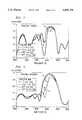
- FIG. 2shows a comparison of the reflectivity versus wavelength for implanted devices as shown in FIG. 1 and for non-implanted devices, when the devices are placed within a Fabry-Perot etalon;
- FIG. 3shows a comparison of the reflectivity versus wavelength for implanted devices as shown in FIG. 1 and for non-implanted devices, wherein the devices have been anti-reflection coated to reduce Fabry-Perot effects;
- FIG. 4shows reflectivity versus applied voltage for devices in Fabry-Perot etalons wherein the devices are both implanted and non-implanted;
- FIG. 5shows responsivity versus applied voltage for devices in Fabry-Perot etalons wherein the devices are both implanted and non-implanted.
- Electro-absorption optical modulatorsdissipate power inside the semiconductor device. Generally, it is desirable to minimize power dissipation because it is a major contributing factor in determining device packing density and device operating parameters such as maximum optical input power.
- An ideal absorption modulatortheoretically dissipates an amount of energy equal to the optical energy absorbed from photons of the incident light beam.
- Absorption of a photon in a semiconductor modulatorgenerates an electron-hole pair having the same total energy as that absorbed from the incident photon.
- the photo-generated carriers, the electron and the holelose an amount of energy equal to that of the absorbed photon. Without radiative recombination, the lost energy is deposited as heat in the semiconductor material of the modulator. This process of losing energy is termed intrinsic dissipation and involves the minimum amount of dissipated energy possible from an absorption event.
- Energy dissipated in excess of the minimumis from non-intrinsic dissipation processes.
- External energy sources connected to the modulatorare the sources of non-intrinsic dissipation. The most common source is from the electromagnetic field used in performing modulation.
- Photo-generated carriersare capable of acquiring energy from the applied field. This energy is then dissipated through the action of photo-current and it may greatly exceed the amount of intrinsic energy dissipation.
- an absorption eventresults in generation of an electron-hole pair with a total energy equal to the bandgap energy of the material, for example, about 1.42 eV in GaAs.
- motion of the photo-generated carriers through a 5 V externally applied potentialdissipates 5 eV of energy which clearly dominates the intrinsic dissipation.
- the present device shown in an exemplary embodiment in FIG. 1utilizes both photocurrent inhibiting techniques.
- techniques for decreasing carrier lifetime in the intrinsic quantum well regiondiminish certain exciton properties which directly affect modulator contrast ratio and the like. But, such techniques can be controlled to retain desirable optical properties such as absorption for the modulator.
- Carrier lifetime in intrinsic multiple quantum well materialis approximately 1 ns.
- electrons transported at saturated carrier velocities on the order of 10 7 cm/sectraverse a 1 ⁇ m region in approximately 10 picoseconds.
- carriersshould be confined within a quantum well until recombination occurs.
- recombination timeshould be made as short as possible to alleviate saturation problems.
- acceptable carrier lifetimes for this exampleare expected to be in the range of 10 picoseconds in order to suppress photocurrent in a significant way.
- Carrier lifetimecomprises radiative and non-radiative components.
- Non-radiative carrier lifetime componentsare most easily controllable in semiconductor material by the introduction of non-radiative carrier recombination centers in the semiconductor quantum well material.
- Non-radiative recombination centersare introduced in semiconductor material by standard techniques such as ion implantation, introduction of deep level impurities, formation of interstitials, formation of vacancies, local clustering of atoms, growth of polycrystalline material, and formation of material having a large number of defects or impurities. While the introduction of non-radiative recombination centers reduces carrier lifetime during optical absorption, it is also desirable to have this semiconductor quantum well material exhibit high resistivity so that the device is inhibited from drawing current from external sources in the absence of incident light.
- FIG. 1An exemplary surface normal, multiple quantum well, p-i-n diode modulator is depicted in FIG. 1.
- This modulatorincludes p and n contact regions, an intrinsic (i) multiple quantum well region, a reflector region, and metallic contacts, all formed on a semiconductor substrate.
- the various semiconductor layersare grown on semi-insulating GaAs substrate 16 by standard epitaxial growth techniques.
- Epitaxial growth techniques for semiconductor compounds such as Group III-V compoundsare well known to persons of ordinary skill in the art and include molecular beam epitaxy (MBE) and metal organic chemical vapor deposition (MOCVD), for example.
- MBEmolecular beam epitaxy
- MOCVDmetal organic chemical vapor deposition
- Reflector region 15is grown on substrate 16.
- Reflector region 15is a semiconductor thin film reflector designed to reflect optical beams propagating in a predetermined band of wavelengths around a desired wavelength, usually the wavelength of the incident optical beam 1.
- the reflector regioncomprises sixteen pairs of layers having an optical thickness ⁇ /4 n where ⁇ is the optical wavelength and n is the effective refractive index of the layer wherein each pair includes a 711 ⁇ layer of AlAs and 599 ⁇ layer of Al 0 .11 Ga 0 .89 As.
- This exemplary layer structurerealizes a reflector for wavelengths in the neighborhood of 850 nm (0.850 ⁇ m).
- Semiconductor layershave been utilized for the reflector region in order to integrate the reflector more easily into the entire semiconductor device.
- the use of the reflector regionis not required when the opaque substrate is etched away to reveal the bottom of contact layer 14 or when the substrate is translucent or transparent at the incident optical wavelength.
- incident optical beamsmake two passes through the p-i-n structure.
- Contact region 14exhibits n-type conductivity.
- a 5000 ⁇ thick layer of Al 0 .11 Ga 0 .89 As doped with silicon at an approximate concentration of 10 18 cm -exhibits n + conductivity for contact region 14.
- Intrinsic quantum well region 13is intentionally undoped and includes narrow bandgap layers interleaved with wide bandgap layers.
- the narrow bandgap layersare called quantum well layers and are sufficiently thin to exhibit quantum size effects, that is, quantization of the available conduction band into discrete energy levels.
- the wide bandgap layersare called barrier layers. While there is no constraint on the thickness of barrier layers, the thickness of each quantum well layer is usually less than several hundred ⁇ .
- the GaAs quantum well layersare approximately 100 ⁇ whereas the Al x Ga 1-x As barrier layers are approximately 60 ⁇ for an Al mole fraction x of 0.7.
- the height of the barrier layeris changed by varying the mole fraction to a value between 0.02 and 1.0. Sixty periods or quantum well/barrier layer pairs are employed in quantum well region 13.
- Contact region 12exhibits p-type conductivity.
- a 5000 ⁇ thick layer of Al 0 .11 Ga 0 .89 As doped with beryllium at an approximate concentration of 10 18 cm -3exhibits p + conductivity for contact region 12. This embodiment assists in localizing the non-radiative recombination centers in the quantum well region.
- contact region 12comprises a 1000 ⁇ p + GaAs cap layer over a 2000 ⁇ p + Al 0 .11 Ga 0 .89 As layer in contact with quantum well region 13. This embodiment does not offer the same extent of localization as the former embodiment.
- Standard photolithography and etching techniqueswere employed to form a mesa device wherein contact is made to underlying contact region 14. Once the mesa is formed, metallic p and n contacts are applied to contact regions 12 and 14, respectively. Standard ohmic contact deposition and alloying techniques are employed to form the particular contacts.
- Anti-reflection coatingshave been applied to surface 17 of the contact region 12. Such anti-reflection coatings reduce reflections from surface 17. Without an anti-reflection coating on surface 17, sufficient reflectivity from the crystallographic plane at surface 17 exists to form a weak Fabry-Perot etalon with reflector region 15. Of course, standard thin film stack reflective layers can be applied to the surface 17 to further increase its reflectivity and the finesse of the resulting Fabry-Perot etalon.
- the reflectivity for a modulator realized in accordance with the principles of the inventionis effectively made equal to the reflectivity for a standard non-implanted p-i-n modulator as depicted in FIGS. 2 and 4.
- Non-radiative recombination centers for suppressing the photocurrentare produced in the intrinsic quantum well region following growth of the modulator. Formation of the recombination centers may be accomplished at various stages in the device processing. Proton implantation is utilized to form the non-radiative recombination centers. The proton energy and the proton dose levels are chosen for the semiconductor material to achieve a sufficient density of non-radiative recombination centers localized or substantially centered in the intrinsic quantum well region.
- a proton energy of 130 keVwas utilized. Dose levels were approximately 1 ⁇ 10 12 cm -2 , 1 ⁇ 10 13 cm -2 , and 1 ⁇ 10 14 cm -2 . From a study of the devices implanted at these dose levels, it was determined that exciton broadening became extreme in this material system for the proton dose of 1 ⁇ 10 14 cm -2 . It was determined that all implanted p-i-n devices exhibited modulator behavior, although performance for anti-reflection coated devices was degraded monotonically with increasing implantation level.
- FIG. 2shows a comparison of reflectivity versus wavelength for two p-i-n modulators operated at two different bias levels.
- the p-i-n modulatorswere formed in a Fabry-Perot etalon and incorporated GaAs quantum well layers and AlAs barrier layers in the intrinsic quantum well region.
- the p-i-n modulatorswere subjected to bias potentials of 0 V and -12.5 V over a range of incident optical wavelengths between 800 nm and 900 nm.
- Curves 21 and 23show the reflectivity for a non-implanted p-i-n modulator.
- Curves 22 and 24show the reflectivity for an implanted (1 ⁇ 10 13 cm -2 ) p-i-n modulator realized in accordance with the inventive principles above.
- FIG. 2shows that the reflectivity and, therefore, the modulation performance is substantially the same for implanted and non-implanted devices placed in a Fabry-Perot etalon.
- FIG. 3shows a comparison of reflectivity versus wavelength for two p-i-n modulators operated at two different bias levels.
- the p-i-n modulatorswere anti-reflection coated on the top surface and incorporated GaAs quantum well layers and AlAs barrier layers in the intrinsic quantum well region.
- the p-i-n modulatorswere subjected to bias potentials of 0 V and -1.25 V over a range of incident optical wavelengths between 800 nm and 900 nm.
- Curves 31 and 33show the reflectivity for a non-implanted p-i-n modulator.
- Curves 32 and 34show the reflectivity for an implanted (1 ⁇ 10 13 cm -2 ) p-i-n modulator realized in accordance with the inventive principles above.
- FIG. 3shows that reflectivity differs under applied bias conditions for implanted and non-implanted devices, both anti-reflection coated.
- FIG. 4shows the reflectivity for two implanted p-i-n devices and one non-implanted device as a function of bias voltage. All devices were subject to a low power incident optical power beam at a wavelength of approximately 856 nm. Curve 41 corresponds to the reflectivity for the non-implanted p-i-n device while curves 42 and 43 show the reflectivity for p-i-n device having implantation dose levels of 1 ⁇ 10 12 cm -2 and 1 ⁇ 10 -- cm -2 , respectively. A comparison of these curves clearly shows that the contrast ratio and, therefore, the modulation performance for the implanted p-i-n modulators are substantially equivalent to that for the non-implanted device.
- FIG. 5shows the responsivity, measured in amps per watt, for two implanted p-i-n devices and one non-implanted p-i-n device as a function of applied bias voltage. Responsivity is defined to be the ratio of photocurrent generated to an incident optical power level. The devices and incident optical power conditions were substantially identical to those utilized in reference to FIG. 4.
- Curve 51corresponds to the reflectivity for the non-implanted p-i-n device while curves 52 and 53 show the reflectivity for p-i-n device having implantation dose levels of 1 ⁇ 10 -12 cm -2 and 1 ⁇ 10 13 cm -2 , respectively.
- Photocurrent suppression for the implanted, quantum well, p-i-n modulatoris achieved when the non-radiative recombination rate for the charge carriers dominates the carrier sweep-out, or collection, rate and the radiative recombination rate.
- the degree of photocurrent suppression and, intuitively, the dominance of the non-radiative .recombination rateare better understood from a relationship stating that, if the non-radiative recombination rate is N times the carrier collection rate and is also much greater than the radiative recombination rate, then the photocurrent will be suppressed by the ratio of 1/(1+N). If N equals 9, then the photocurrent will be approximately one-tenth that of the modulator without non-radiative recombination centers.
- non-radiative recombination rateis proportional to the number of non-radiative recombination centers per unit volume of material.
- degree of exciton broadening in the quantum wellsis also proportional to the number of non-radiative recombination centers per unit volume of material.
- GaAs/AlAs and GaAs/AlGaAsare described above for fabricating the semiconductor modulator structure, other material may be selected for other semiconductor Group III-V systems such as InGaAs/InAlAs, InGaAs/InGaAlAs, GaAsSb/GaAlAsSb, and InGaAsP/InP.
- the layersmay be lattice matched to suitable GaAs or InP substrates. Mismatching is also contemplated wherein strained layers are grown over substrate material.
- extension of the device structuresis also contemplated to semiconductor compounds in Group TI-VI and Group IV.
- the device structure described aboveis operated in the reflection mode. It is contemplated that the use of transparent substrate material or even the etching of a shallow recess into the substrate to permit more effective light transmission through the modulator is desirable for operating the device as a transmissive mode modulator. That is, the light is incident on the top surface of the modulator and exits through the bottom surface thereof or vice versa. Such techniques are well known among persons of ordinary skill in the art.
Landscapes
- Physics & Mathematics (AREA)
- Nonlinear Science (AREA)
- Optics & Photonics (AREA)
- Chemical & Material Sciences (AREA)
- Engineering & Computer Science (AREA)
- Nanotechnology (AREA)
- General Physics & Mathematics (AREA)
- Life Sciences & Earth Sciences (AREA)
- Biophysics (AREA)
- Crystallography & Structural Chemistry (AREA)
- Optical Modulation, Optical Deflection, Nonlinear Optics, Optical Demodulation, Optical Logic Elements (AREA)
Abstract
Description
Claims (8)
Priority Applications (1)
| Application Number | Priority Date | Filing Date | Title |
|---|---|---|---|
| US07/954,201US5436756A (en) | 1992-09-30 | 1992-09-30 | Suppressed photocurrent, quantum well optical modulation device |
Applications Claiming Priority (1)
| Application Number | Priority Date | Filing Date | Title |
|---|---|---|---|
| US07/954,201US5436756A (en) | 1992-09-30 | 1992-09-30 | Suppressed photocurrent, quantum well optical modulation device |
Publications (1)
| Publication Number | Publication Date |
|---|---|
| US5436756Atrue US5436756A (en) | 1995-07-25 |
Family
ID=25495082
Family Applications (1)
| Application Number | Title | Priority Date | Filing Date |
|---|---|---|---|
| US07/954,201Expired - LifetimeUS5436756A (en) | 1992-09-30 | 1992-09-30 | Suppressed photocurrent, quantum well optical modulation device |
Country Status (1)
| Country | Link |
|---|---|
| US (1) | US5436756A (en) |
Cited By (23)
| Publication number | Priority date | Publication date | Assignee | Title |
|---|---|---|---|---|
| US5627854A (en)* | 1995-03-15 | 1997-05-06 | Lucent Technologies Inc. | Saturable bragg reflector |
| US5689357A (en)* | 1994-12-23 | 1997-11-18 | Cselt- Centro Studi E Laboratori Telecomunicazioni S.P.A. | Nonlinear optical element for extremely high bit rates |
| US5872016A (en)* | 1996-06-18 | 1999-02-16 | Lucent Technologies Inc. | Process of making an optoelectronic devices utilizing multiple quantum well pin structures |
| WO2002061498A1 (en)* | 2001-01-30 | 2002-08-08 | 3Dv Systems, Ltd. | Optical modulator |
| US20030169195A1 (en)* | 2002-03-08 | 2003-09-11 | Quellan, Inc. | High-speed analog-to-digital converter using a unique gray code |
| US20030184837A1 (en)* | 2000-07-11 | 2003-10-02 | Alexandre Marceaux | Saturable absorbent structure, in particular for regenerating optical component and method for making same |
| US7035361B2 (en) | 2002-07-15 | 2006-04-25 | Quellan, Inc. | Adaptive noise filtering and equalization for optimal high speed multilevel signal decoding |
| US7050388B2 (en) | 2003-08-07 | 2006-05-23 | Quellan, Inc. | Method and system for crosstalk cancellation |
| US7123676B2 (en) | 2003-11-17 | 2006-10-17 | Quellan, Inc. | Method and system for antenna interference cancellation |
| US7149256B2 (en) | 2001-03-29 | 2006-12-12 | Quellan, Inc. | Multilevel pulse position modulation for efficient fiber optic communication |
| US7173551B2 (en) | 2000-12-21 | 2007-02-06 | Quellan, Inc. | Increasing data throughput in optical fiber transmission systems |
| US7212580B2 (en) | 2002-02-15 | 2007-05-01 | Quellan, Inc. | Multi-level signal clock recovery technique |
| US7215721B2 (en) | 2001-04-04 | 2007-05-08 | Quellan, Inc. | Method and system for decoding multilevel signals |
| US7307569B2 (en) | 2001-03-29 | 2007-12-11 | Quellan, Inc. | Increasing data throughput in optical fiber transmission systems |
| US7522883B2 (en) | 2004-12-14 | 2009-04-21 | Quellan, Inc. | Method and system for reducing signal interference |
| US7616700B2 (en) | 2003-12-22 | 2009-11-10 | Quellan, Inc. | Method and system for slicing a communication signal |
| US7725079B2 (en) | 2004-12-14 | 2010-05-25 | Quellan, Inc. | Method and system for automatic control in an interference cancellation device |
| US7804760B2 (en) | 2003-08-07 | 2010-09-28 | Quellan, Inc. | Method and system for signal emulation |
| US7934144B2 (en) | 2002-11-12 | 2011-04-26 | Quellan, Inc. | High-speed analog-to-digital conversion with improved robustness to timing uncertainty |
| US20120153417A1 (en)* | 2010-12-16 | 2012-06-21 | National Central University | Laser Power Converter for Data Detection and Optical-to-Electrical Power Generation |
| US9252983B2 (en) | 2006-04-26 | 2016-02-02 | Intersil Americas LLC | Method and system for reducing radiated emissions from a communications channel |
| US10411807B1 (en) | 2018-04-05 | 2019-09-10 | Nokia Solutions And Networks Oy | Optical transmitter having an array of surface-coupled electro-absorption modulators |
| US10727948B2 (en) | 2018-04-05 | 2020-07-28 | Nokia Solutions And Networks Oy | Communication system employing surface-coupled optical devices |
Citations (4)
| Publication number | Priority date | Publication date | Assignee | Title |
|---|---|---|---|---|
| US5008717A (en)* | 1989-03-03 | 1991-04-16 | At&T Bell Laboratories | Semiconductor device including cascaded modulation-doped quantum well heterostructures |
| US5105301A (en)* | 1989-01-26 | 1992-04-14 | Cselt - Centro Studi E Laboratori Telecommunicazioni S.P.A. | Coupled quantum-well electro-optical modulator |
| US5115335A (en)* | 1990-06-29 | 1992-05-19 | The United States Of America As Represented By The Secretary Of The Air Force | Electrooptic fabry-perot pixels for phase-dominant spatial light modulators |
| US5216260A (en)* | 1984-11-19 | 1993-06-01 | Max-Planck Gesellschaft Zur Foerderung Der Wissenschaften E.V. | Optically bistable semiconductor device with pairs of monoatomic layers separated by intrinsic layers |
- 1992
- 1992-09-30USUS07/954,201patent/US5436756A/ennot_activeExpired - Lifetime
Patent Citations (4)
| Publication number | Priority date | Publication date | Assignee | Title |
|---|---|---|---|---|
| US5216260A (en)* | 1984-11-19 | 1993-06-01 | Max-Planck Gesellschaft Zur Foerderung Der Wissenschaften E.V. | Optically bistable semiconductor device with pairs of monoatomic layers separated by intrinsic layers |
| US5105301A (en)* | 1989-01-26 | 1992-04-14 | Cselt - Centro Studi E Laboratori Telecommunicazioni S.P.A. | Coupled quantum-well electro-optical modulator |
| US5008717A (en)* | 1989-03-03 | 1991-04-16 | At&T Bell Laboratories | Semiconductor device including cascaded modulation-doped quantum well heterostructures |
| US5115335A (en)* | 1990-06-29 | 1992-05-19 | The United States Of America As Represented By The Secretary Of The Air Force | Electrooptic fabry-perot pixels for phase-dominant spatial light modulators |
Non-Patent Citations (14)
| Title |
|---|
| D. A. B. Miller et al., Physical Review Letters, vol. 53, No. 22, Nov. 26, 1984, "Band-Edge Electroabsorption in Quantum Well Structures: The Quantum-Confined Stark Effect," pp. 2173-2176. |
| D. A. B. Miller et al., Physical Review Letters, vol. 53, No. 22, Nov. 26, 1984, Band Edge Electroabsorption in Quantum Well Structures: The Quantum Confined Stark Effect, pp. 2173 2176.* |
| D. A. B. Miller, Optical and Quantum Electronics, vol. 22, 1990, "Quantum-Well Self-Electro-Optic Effect Devicss," pp. S61-S98. |
| D. A. B. Miller, Optical and Quantum Electronics, vol. 22, 1990, Quantum Well Self Electro Optic Effect Devicss, pp. S61 S98.* |
| M. Lambsdorff et al., Applied Physics Letters, vol. 58, No. 17, Apr. 29, 1991, "Subpicosecond Carrier Lifetimes in Radiation-Damaged GaAs," pp. 1881-1883. |
| M. Lambsdorff et al., Applied Physics Letters, vol. 58, No. 17, Apr. 29, 1991, Subpicosecond Carrier Lifetimes in Radiation Damaged GaAs, pp. 1881 1883.* |
| M. Wegener et al., Applied Physics Letters, vol. 55, No. 6, Aug. 7, 1989, "Electroabsorption and Refraction by Electron Transfer in Asymmetric Modulation-Doped Multiple Well Structures," pp. 583-585. |
| M. Wegener et al., Applied Physics Letters, vol. 55, No. 6, Aug. 7, 1989, Electroabsorption and Refraction by Electron Transfer in Asymmetric Modulation Doped Multiple Well Structures, pp. 583 585.* |
| T. K. Woodward et al., Applied Physics Letters, vol. 60, No. 6, Feb. 10, 1992, "Suppressed Photocurrent Multiple-Quantum-Well Optical Modulators by Proton Implantation," pp. 742-744. |
| T. K. Woodward et al., Applied Physics Letters, vol. 60, No. 6, Feb. 10, 1992, Suppressed Photocurrent Multiple Quantum Well Optical Modulators by Proton Implantation, pp. 742 744.* |
| W. H. Knox et al., Applied Physics Letters, vol. 59, No. 12, Sep. 16, 1991, "Low-Temperature-Grown GaAs Quantum Wells: Femtosecond Nonlinear Optical and Parallel-Field Transport Studies," pp. 1491-1493. |
| W. H. Knox et al., Applied Physics Letters, vol. 59, No. 12, Sep. 16, 1991, Low Temperature Grown GaAs Quantum Wells: Femtosecond Nonlinear Optical and Parallel Field Transport Studies, pp. 1491 1493.* |
| Y. Silberberg et al., Applied Physics Letters, vol. 46, No. 8, Apr. 15, 1985, "Fast Nonlinear Optical Response from Proton-Bombarded Multiple Quantum Well Structure," pp. 701-703. |
| Y. Silberberg et al., Applied Physics Letters, vol. 46, No. 8, Apr. 15, 1985, Fast Nonlinear Optical Response from Proton Bombarded Multiple Quantum Well Structure, pp. 701 703.* |
Cited By (42)
| Publication number | Priority date | Publication date | Assignee | Title |
|---|---|---|---|---|
| US5689357A (en)* | 1994-12-23 | 1997-11-18 | Cselt- Centro Studi E Laboratori Telecomunicazioni S.P.A. | Nonlinear optical element for extremely high bit rates |
| US5627854A (en)* | 1995-03-15 | 1997-05-06 | Lucent Technologies Inc. | Saturable bragg reflector |
| US5872016A (en)* | 1996-06-18 | 1999-02-16 | Lucent Technologies Inc. | Process of making an optoelectronic devices utilizing multiple quantum well pin structures |
| US20030184837A1 (en)* | 2000-07-11 | 2003-10-02 | Alexandre Marceaux | Saturable absorbent structure, in particular for regenerating optical component and method for making same |
| US7173551B2 (en) | 2000-12-21 | 2007-02-06 | Quellan, Inc. | Increasing data throughput in optical fiber transmission systems |
| US6999219B2 (en) | 2001-01-30 | 2006-02-14 | 3Dv Systems, Ltd. | Optical modulator |
| WO2002061498A1 (en)* | 2001-01-30 | 2002-08-08 | 3Dv Systems, Ltd. | Optical modulator |
| US20040125429A1 (en)* | 2001-01-30 | 2004-07-01 | Amnon Manassen | Optical modulator |
| JP2004520617A (en)* | 2001-01-30 | 2004-07-08 | スリーディーヴィー システムズ リミテッド | Light modulator |
| US7352824B2 (en) | 2001-03-29 | 2008-04-01 | Quellan, Inc. | Multilevel pulse position modulation for efficient fiber optic communication |
| US7307569B2 (en) | 2001-03-29 | 2007-12-11 | Quellan, Inc. | Increasing data throughput in optical fiber transmission systems |
| US7149256B2 (en) | 2001-03-29 | 2006-12-12 | Quellan, Inc. | Multilevel pulse position modulation for efficient fiber optic communication |
| US7602860B2 (en) | 2001-04-04 | 2009-10-13 | Quellan, Inc. | Method and system for decoding multilevel signals |
| US7215721B2 (en) | 2001-04-04 | 2007-05-08 | Quellan, Inc. | Method and system for decoding multilevel signals |
| US7212580B2 (en) | 2002-02-15 | 2007-05-01 | Quellan, Inc. | Multi-level signal clock recovery technique |
| US20030169195A1 (en)* | 2002-03-08 | 2003-09-11 | Quellan, Inc. | High-speed analog-to-digital converter using a unique gray code |
| US6816101B2 (en) | 2002-03-08 | 2004-11-09 | Quelian, Inc. | High-speed analog-to-digital converter using a unique gray code |
| US7573966B2 (en) | 2002-07-15 | 2009-08-11 | Quellan, Inc. | Adaptive noise filtering and equalization for optimal high speed multilevel signal decoding |
| US8311168B2 (en) | 2002-07-15 | 2012-11-13 | Quellan, Inc. | Adaptive noise filtering and equalization for optimal high speed multilevel signal decoding |
| US7035361B2 (en) | 2002-07-15 | 2006-04-25 | Quellan, Inc. | Adaptive noise filtering and equalization for optimal high speed multilevel signal decoding |
| US7934144B2 (en) | 2002-11-12 | 2011-04-26 | Quellan, Inc. | High-speed analog-to-digital conversion with improved robustness to timing uncertainty |
| US7804760B2 (en) | 2003-08-07 | 2010-09-28 | Quellan, Inc. | Method and system for signal emulation |
| US8605566B2 (en) | 2003-08-07 | 2013-12-10 | Quellan, Inc. | Method and system for signal emulation |
| US8068406B2 (en) | 2003-08-07 | 2011-11-29 | Quellan, Inc. | Method and system for crosstalk cancellation |
| US7050388B2 (en) | 2003-08-07 | 2006-05-23 | Quellan, Inc. | Method and system for crosstalk cancellation |
| US7626916B2 (en) | 2003-08-07 | 2009-12-01 | Quellan, Inc. | Method and system for crosstalk cancellation |
| US20080146183A1 (en)* | 2003-11-17 | 2008-06-19 | Quellan, Inc. | Method and system for antenna interference cancellation |
| US7366244B2 (en) | 2003-11-17 | 2008-04-29 | Quellan, Inc. | Method and system for antenna interference cancellation |
| US7123676B2 (en) | 2003-11-17 | 2006-10-17 | Quellan, Inc. | Method and system for antenna interference cancellation |
| US7729431B2 (en) | 2003-11-17 | 2010-06-01 | Quellan, Inc. | Method and system for antenna interference cancellation |
| US7616700B2 (en) | 2003-12-22 | 2009-11-10 | Quellan, Inc. | Method and system for slicing a communication signal |
| US8576939B2 (en) | 2003-12-22 | 2013-11-05 | Quellan, Inc. | Method and system for slicing a communication signal |
| US8503940B2 (en) | 2004-12-14 | 2013-08-06 | Quellan, Inc. | Reducing signal interference |
| US8135350B2 (en) | 2004-12-14 | 2012-03-13 | Quellan, Inc. | System for reducing signal interference |
| US7522883B2 (en) | 2004-12-14 | 2009-04-21 | Quellan, Inc. | Method and system for reducing signal interference |
| US8005430B2 (en) | 2004-12-14 | 2011-08-23 | Quellan Inc. | Method and system for reducing signal interference |
| US7725079B2 (en) | 2004-12-14 | 2010-05-25 | Quellan, Inc. | Method and system for automatic control in an interference cancellation device |
| US9252983B2 (en) | 2006-04-26 | 2016-02-02 | Intersil Americas LLC | Method and system for reducing radiated emissions from a communications channel |
| US20120153417A1 (en)* | 2010-12-16 | 2012-06-21 | National Central University | Laser Power Converter for Data Detection and Optical-to-Electrical Power Generation |
| US8368162B2 (en)* | 2010-12-16 | 2013-02-05 | National Central University | Laser power converter for data detection and optical-to-electrical power generation |
| US10411807B1 (en) | 2018-04-05 | 2019-09-10 | Nokia Solutions And Networks Oy | Optical transmitter having an array of surface-coupled electro-absorption modulators |
| US10727948B2 (en) | 2018-04-05 | 2020-07-28 | Nokia Solutions And Networks Oy | Communication system employing surface-coupled optical devices |
Similar Documents
| Publication | Publication Date | Title |
|---|---|---|
| US5436756A (en) | Suppressed photocurrent, quantum well optical modulation device | |
| EP0135582B1 (en) | Semiconductor device for controlling light using multiple quantum wells | |
| US5018157A (en) | Vertical cavity semiconductor lasers | |
| JPH04276681A (en) | Vertical cavity surface light-emitting laser provided with transparent electrode | |
| US5315430A (en) | Strained layer Fabry-Perot device | |
| JPH0728047B2 (en) | Phototransistor | |
| US5210428A (en) | Semiconductor device having shallow quantum well region | |
| US4904859A (en) | Self electrooptic effect device employing asymmetric quantum wells | |
| US4795225A (en) | Semiconductor optical switch | |
| GB2114768A (en) | Bistable optical device | |
| EP0437936B1 (en) | Optical processing using a multilayer heterostructure | |
| KR100192926B1 (en) | Quantum well structures | |
| US5027178A (en) | Electrically tunable interference filters and methods for their use | |
| US7142342B2 (en) | Electroabsorption modulator | |
| US4913506A (en) | Optical modulation device | |
| US5093695A (en) | Controllable semiconductor modulator having interleaved contacts | |
| US5343054A (en) | Semiconductor light-detection device with recombination rates | |
| US5637883A (en) | Optically addressed spatial light modulator using an intrinsic semiconductor active material and high resistivity cladding layers | |
| Woodward et al. | Suppressed photocurrent multiple‐quantum‐well optical modulators by proton implantation | |
| US5072272A (en) | Semiconductor light modulator with pn layers | |
| Lord et al. | Electroabsorption modulators operating at 1.3 μm on GaAs substrates | |
| Lee et al. | Symmetric self‐electro‐optic effect device array grown by metalorganic vapor phase epitaxy using GaAs/Al0. 04Ga0. 96As shallow quantum wells | |
| Tobin et al. | Quantum-confined Stark effect modulator based on multiple triple-quantum wells | |
| EP0385638A2 (en) | Semiconductor superlattice self-electrooptic effect device | |
| CA1037133A (en) | Digital optical computer techniques |
Legal Events
| Date | Code | Title | Description |
|---|---|---|---|
| AS | Assignment | Owner name:AMERICAN TELEPHONE AND TELEGRAPH COMPANY, NEW YORK Free format text:ASSIGNMENT OF ASSIGNORS INTEREST.;ASSIGNORS:KNOX, WAYNE H.;STARK, JASON B.;TELL, BENJAMIN;AND OTHERS;REEL/FRAME:006283/0771 Effective date:19920930 | |
| AS | Assignment | Owner name:AT&T CORP., NEW YORK Free format text:ASSIGNMENT OF ASSIGNORS INTEREST;ASSIGNOR:AMERICAN TELELPHONE AND TELEGRAPH COMPANY;REEL/FRAME:007527/0274 Effective date:19940420 Owner name:AT&T IPM CORP., FLORIDA Free format text:ASSIGNMENT OF ASSIGNORS INTEREST;ASSIGNOR:AT&T CORP.;REEL/FRAME:007528/0038 Effective date:19950523 | |
| STCF | Information on status: patent grant | Free format text:PATENTED CASE | |
| FEPP | Fee payment procedure | Free format text:PAYOR NUMBER ASSIGNED (ORIGINAL EVENT CODE: ASPN); ENTITY STATUS OF PATENT OWNER: LARGE ENTITY | |
| FPAY | Fee payment | Year of fee payment:4 | |
| FEPP | Fee payment procedure | Free format text:PAYER NUMBER DE-ASSIGNED (ORIGINAL EVENT CODE: RMPN); ENTITY STATUS OF PATENT OWNER: LARGE ENTITY Free format text:PAYOR NUMBER ASSIGNED (ORIGINAL EVENT CODE: ASPN); ENTITY STATUS OF PATENT OWNER: LARGE ENTITY | |
| FPAY | Fee payment | Year of fee payment:8 | |
| FPAY | Fee payment | Year of fee payment:12 |