US5436744A - Flexible liquid crystal display with integrated driver circuit and display electrodes formed on opposite sides of folded substrate - Google Patents
Flexible liquid crystal display with integrated driver circuit and display electrodes formed on opposite sides of folded substrateDownload PDFInfo
- Publication number
- US5436744A US5436744AUS08/115,625US11562593AUS5436744AUS 5436744 AUS5436744 AUS 5436744AUS 11562593 AUS11562593 AUS 11562593AUS 5436744 AUS5436744 AUS 5436744A
- Authority
- US
- United States
- Prior art keywords
- liquid crystal
- flexible substrate
- substrate
- crystal display
- conductive vias
- Prior art date
- Legal status (The legal status is an assumption and is not a legal conclusion. Google has not performed a legal analysis and makes no representation as to the accuracy of the status listed.)
- Expired - Lifetime
Links
- 239000000758substrateSubstances0.000titleclaimsabstractdescription74
- 230000009975flexible effectEffects0.000titleclaimsabstractdescription42
- 239000004973liquid crystal related substanceSubstances0.000titleclaimsabstractdescription29
- 239000000463materialSubstances0.000claimsabstractdescription11
- RYGMFSIKBFXOCR-UHFFFAOYSA-NCopperChemical compound[Cu]RYGMFSIKBFXOCR-UHFFFAOYSA-N0.000claimsabstractdescription6
- 239000007767bonding agentSubstances0.000claimsabstractdescription6
- 229910052802copperInorganic materials0.000claimsabstractdescription6
- 239000010949copperSubstances0.000claimsabstractdescription6
- 229920000728polyesterPolymers0.000claimsdescription2
- AMGQUBHHOARCQH-UHFFFAOYSA-Nindium;oxotinChemical compound[In].[Sn]=OAMGQUBHHOARCQH-UHFFFAOYSA-N0.000claims5
- APFVFJFRJDLVQX-UHFFFAOYSA-Nindium atomChemical compound[In]APFVFJFRJDLVQX-UHFFFAOYSA-N0.000abstractdescription6
- 229910003437indium oxideInorganic materials0.000abstractdescription6
- XOLBLPGZBRYERU-UHFFFAOYSA-Ntin dioxideChemical compoundO=[Sn]=OXOLBLPGZBRYERU-UHFFFAOYSA-N0.000abstractdescription6
- 229910001887tin oxideInorganic materials0.000abstractdescription6
- 238000004026adhesive bondingMethods0.000abstract1
- 239000000853adhesiveSubstances0.000description4
- 230000001070adhesive effectEffects0.000description4
- 239000004593EpoxySubstances0.000description3
- PXHVJJICTQNCMI-UHFFFAOYSA-NNickelChemical compound[Ni]PXHVJJICTQNCMI-UHFFFAOYSA-N0.000description2
- 238000013459approachMethods0.000description2
- 230000008878couplingEffects0.000description2
- 238000010168coupling processMethods0.000description2
- 238000005859coupling reactionMethods0.000description2
- 239000011521glassSubstances0.000description2
- 238000001465metallisationMethods0.000description2
- 229920003023plasticPolymers0.000description2
- BASFCYQUMIYNBI-UHFFFAOYSA-NplatinumChemical compound[Pt]BASFCYQUMIYNBI-UHFFFAOYSA-N0.000description2
- 238000007789sealingMethods0.000description2
- ATJFFYVFTNAWJD-UHFFFAOYSA-NTinChemical compound[Sn]ATJFFYVFTNAWJD-UHFFFAOYSA-N0.000description1
- 229910052782aluminiumInorganic materials0.000description1
- XAGFODPZIPBFFR-UHFFFAOYSA-NaluminiumChemical compound[Al]XAGFODPZIPBFFR-UHFFFAOYSA-N0.000description1
- 238000000151depositionMethods0.000description1
- 238000005553drillingMethods0.000description1
- 229920001971elastomerPolymers0.000description1
- 239000000806elastomerSubstances0.000description1
- 238000005530etchingMethods0.000description1
- 229920002457flexible plasticPolymers0.000description1
- PCHJSUWPFVWCPO-UHFFFAOYSA-NgoldChemical compound[Au]PCHJSUWPFVWCPO-UHFFFAOYSA-N0.000description1
- 229910052737goldInorganic materials0.000description1
- 239000010931goldSubstances0.000description1
- 239000012943hotmeltSubstances0.000description1
- 229910052751metalInorganic materials0.000description1
- 239000002184metalSubstances0.000description1
- 238000000034methodMethods0.000description1
- 238000012986modificationMethods0.000description1
- 230000004048modificationEffects0.000description1
- 229910052759nickelInorganic materials0.000description1
- 238000004806packaging method and processMethods0.000description1
- 238000000206photolithographyMethods0.000description1
- 229910052697platinumInorganic materials0.000description1
- 230000000717retained effectEffects0.000description1
- 229910000679solderInorganic materials0.000description1
- 125000006850spacer groupChemical group0.000description1
- 238000004544sputter depositionMethods0.000description1
- 238000006467substitution reactionMethods0.000description1
- 229910052718tinInorganic materials0.000description1
- 239000011135tinSubstances0.000description1
Images


Classifications
- G—PHYSICS
- G02—OPTICS
- G02F—OPTICAL DEVICES OR ARRANGEMENTS FOR THE CONTROL OF LIGHT BY MODIFICATION OF THE OPTICAL PROPERTIES OF THE MEDIA OF THE ELEMENTS INVOLVED THEREIN; NON-LINEAR OPTICS; FREQUENCY-CHANGING OF LIGHT; OPTICAL LOGIC ELEMENTS; OPTICAL ANALOGUE/DIGITAL CONVERTERS
- G02F1/00—Devices or arrangements for the control of the intensity, colour, phase, polarisation or direction of light arriving from an independent light source, e.g. switching, gating or modulating; Non-linear optics
- G02F1/01—Devices or arrangements for the control of the intensity, colour, phase, polarisation or direction of light arriving from an independent light source, e.g. switching, gating or modulating; Non-linear optics for the control of the intensity, phase, polarisation or colour
- G02F1/13—Devices or arrangements for the control of the intensity, colour, phase, polarisation or direction of light arriving from an independent light source, e.g. switching, gating or modulating; Non-linear optics for the control of the intensity, phase, polarisation or colour based on liquid crystals, e.g. single liquid crystal display cells
- G02F1/133—Constructional arrangements; Operation of liquid crystal cells; Circuit arrangements
- G02F1/1333—Constructional arrangements; Manufacturing methods
- G02F1/1345—Conductors connecting electrodes to cell terminals
- G02F1/13452—Conductors connecting driver circuitry and terminals of panels
Definitions
- This inventionrelates in general to a liquid crystal display device and more particularly, to a liquid crystal display device which integrally combines the liquid crystal element and the circuitry for driving the liquid crystal element.
- LCDliquid crystal displays
- Sophisticated driving circuitryis necessary in order to energize selected segments of the LCD to create the desired image.
- the drive circuitryis typically an integrated circuit or microprocessor.
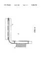
- FIG. 1A typical configuration is shown in FIG. 1 where an LCD 5 is coupled to a printed circuit board 20 that has a driver circuit 30 attached thereto.
- the driver circuit 30is coupled to the LCD 5 by conductive elastomers 40 that are sandwiched between the LCD and the printed circuit board.
- a clamping means 50typically clips, brackets or screws, is used to apply compressive force to the LCD 5 and the printed circuit board 20 in order to clamp the entire structure together. It can be clearly seen from the drawings that this type of structure is quite complex and very thick, thereby limiting its use in applications where thin and light products are required.
- FIG. 2shows another approach utilized in the prior art where the LCD 5 is coupled to the drive circuitry 30 by a flexible circuit 22. Electrical connection between the flex circuit and the LCD is made by an intermediate flexible coupling or by a conductive adhesive 24.
- a liquid crystal display moduleThe liquid crystal display (LCD) is made by creating a film electrode on the surface of a flexible substrate.
- the film electrodeis connected to conductive vias in the flexible substrate by conductive runners.
- the viasare further connected to a circuitry pattern on an opposite side of the flexible substrate.
- a display driveris attached to the circuitry pattern to drive the LCD.
- a second substrate, having a film electrode on it,is arranged in mutually opposing planar relationship to the flexible substrate in order to form a liquid crystal display.
- a liquid crystal materialis then filled in the gap between the two substrates creating an LCD module.
- the LCD moduleis folded about a portion of the flexible substrate so that the display driver circuit is directly underneath the film electrode.
- a bonding agentsuch as an adhesive, may be used to retain the flexible substrate in the folded position.
- the electrodesare indium/tin oxide and the conductive runners connecting the electrodes to the vias are layers of copper over the indium/tin oxide.
- FIG. 1is a cross-sectional view of a conventional liquid crystal display module in accordance with the prior art.
- FIG. 2is a cross-sectional view of another embodiment of the prior art.
- FIG. 3is a plan view of the top side of a flexible substrate in accordance with the present invention.
- FIG. 4is a plan view of the bottom side of the flexible substrate shown in FIG. 3.
- FIG. 5is a cross-sectional view through section 5--5 of FIG. 3.
- FIG. 6is a view of the module shown in FIG. 5 after folding 180°.
- FIGS. 7 and 8are cross-sectional view of alternate embodiments of the invention.
- a liquid crystal display (LCD) package 10is formed by creating a circuitry pattern 62 on a flexible substrate 60.
- the flexible substrateis typically thin plastic material, for example, polyesters.
- the circuitry pattern 62consists of several portions, a first portion being the electrode segments 64. These segments make up the features that are to be shown in the finished display.
- FIG. 3shows a typical seven segment element that is used in numeric displays.
- Each segment of the electrode 64has an accompanying conductive runner 66 that connects the electrodes to a driver circuit.
- the conductive runners 66are also connected to conductive vias or plated through holes 68. These conductive vias are formed in a conventional manner through the substrate, for example, by drilling, etching, stamping, lasing, etc.
- FIG. 4shows the backside of the substrate 60 and one type of connecting methodology whereby the display driver 70 can be connected to the conductive runners 66 by means of the conductive vias 68.
- the electrode 64 and the conductive runners 66are formed by depositing, for example, using sputtering, a layer of indium/tin oxide (ITO) on the substrate and delineating it using conventional photolithography.
- the conductive runners 66are further sputtered or plated with a subsequent layer of copper in order to create a more robust line to allow folding in later operations.
- the dashed line 72 in FIGS. 3 and 4shows an area where the display may be folded. Portions of the conductive runner 66 in this area are metallized with the copper overlayer.
- Other metallization systemsfor example, aluminum, nickel, tin, gold, platinum, and so on, may be used to similarly add mechanical strength to the conductive runners.
- a top substrate 80contains a top electrode 82 also formed in a conventional manner.
- the top substrate 80may be a rigid substrate, such as glass, which is normally used in conventional liquid crystals displays, or it may also be a flexible plastic material similar to the flexible substrate 60 used for the bottom.
- the top substrate 80is bonded to the flexible substrate 60 using a sealing means 84 around the perimeter of the substrate. Sealing means 84 is typically an epoxy or other type of adhesive used to hold the two substrates together and also to seal in the liquid crystal material 86.
- the top substrate 80 and the bottom substrate 60are arranged in a mutually opposing planar relationship normally found in LCD structures.
- the top substrate 80only covers a portion of the bottom substrate 60, that portion being represented by the upper half of the figure above the dashed line 72 in FIG. 3. This is referred to as the display area of the LCD package 10.
- the conductive runners 66are connected to the conductive vias 68 and further to the display driver 70.
- the display driver 70is on the back side of the flexible substrate 60 or opposite the display area.
- the display driver 70is attached to the conductive runners by any of a number of conventional means, such as low-temperature solder, conductive epoxy, and other conductive media.
- FIG. 6shows an alternate embodiment of the invention wherein the fold is made in an opposite direction and only in an approximate 90° bend.
- FIG. 8shows a further embodiment of the invention wherein the display driver 70 is mounted on the same side of the flexible substrate 60 as the display electrode.
- the packagecan be folded 90° as shown, or folded another 90° to make the display driver 70 lie directly below the display area but on an opposite side.
- This configurationwould be similar to that shown in FIG. 6, but the display driver 70 would now be on the exterior of the package rather than the interior.
- a bonding agentmight be employed in order to retain the flexible substrate in the "folded position.”
- the drawing figuresshow but a few embodiments of the invention and it would be clear to one skilled in the art that other configurations and folding schemes might be envisioned as required by the design of the particular LCD package. For example, multiple folds might be made in the flexible substrate, or the flexible substrate might be bent through other angles, such as 45°, 30°, etc., in order to create other package configurations.
- the instant inventionprovides one with numerous options of folding and packaging an LCD package that provides a display driver circuit on the same substrate as the LCD and also provides a much smaller, lighter and more compact package.
- the instant inventionutilizes the flexible properties of a plastic substrate and a flexible metallization system integrated into one piece which forms the substrate of the liquid crystal display.
- the display section of the substrateprovides some of the needed rigidity to the LCD.
- the addition of the flexible metal system to the flexible substrateprovides a unique and novel package to attach the driver circuitry to the display without the need for additional flex circuits, interconnects, and substrates as normally found in the conventional art.
Landscapes
- Physics & Mathematics (AREA)
- Nonlinear Science (AREA)
- Mathematical Physics (AREA)
- Chemical & Material Sciences (AREA)
- Crystallography & Structural Chemistry (AREA)
- General Physics & Mathematics (AREA)
- Optics & Photonics (AREA)
- Devices For Indicating Variable Information By Combining Individual Elements (AREA)
- Liquid Crystal (AREA)
Abstract
Description
This invention relates in general to a liquid crystal display device and more particularly, to a liquid crystal display device which integrally combines the liquid crystal element and the circuitry for driving the liquid crystal element.
Electronic devices that use liquid crystal displays (LCD) have been steadily expanding in popularity. As a consequence, the need to produce LCDs having reduced weight and thickness is widely recognized. Typical LCDs use glass substrates with transparent electrodes and a liquid crystal material placed in a gap between the electrodes. Sophisticated driving circuitry is necessary in order to energize selected segments of the LCD to create the desired image. The drive circuitry is typically an integrated circuit or microprocessor.
The problem of connecting the drive circuitry to the LCD has created a number of solutions in the literature. A typical configuration is shown in FIG. 1 where anLCD 5 is coupled to a printedcircuit board 20 that has adriver circuit 30 attached thereto. Thedriver circuit 30 is coupled to theLCD 5 byconductive elastomers 40 that are sandwiched between the LCD and the printed circuit board. A clamping means 50, typically clips, brackets or screws, is used to apply compressive force to theLCD 5 and the printedcircuit board 20 in order to clamp the entire structure together. It can be clearly seen from the drawings that this type of structure is quite complex and very thick, thereby limiting its use in applications where thin and light products are required.
FIG. 2 shows another approach utilized in the prior art where theLCD 5 is coupled to thedrive circuitry 30 by aflexible circuit 22. Electrical connection between the flex circuit and the LCD is made by an intermediate flexible coupling or by aconductive adhesive 24.
It is clear that prior art approaches to coupling the driver circuitry to the LCD leaves much to be desired. It would be highly advantageous if an LCD package could be made that results in an LCD with lower profile and smaller area that is also less complex to assemble than conventional systems.
Briefly, according to the invention, there is provided a liquid crystal display module. The liquid crystal display (LCD) is made by creating a film electrode on the surface of a flexible substrate. The film electrode is connected to conductive vias in the flexible substrate by conductive runners. The vias are further connected to a circuitry pattern on an opposite side of the flexible substrate. A display driver is attached to the circuitry pattern to drive the LCD. A second substrate, having a film electrode on it, is arranged in mutually opposing planar relationship to the flexible substrate in order to form a liquid crystal display. A liquid crystal material is then filled in the gap between the two substrates creating an LCD module.
In another embodiment of the invention, the LCD module is folded about a portion of the flexible substrate so that the display driver circuit is directly underneath the film electrode. A bonding agent, such as an adhesive, may be used to retain the flexible substrate in the folded position.
In a further embodiment of the invention, the electrodes are indium/tin oxide and the conductive runners connecting the electrodes to the vias are layers of copper over the indium/tin oxide.
FIG. 1 is a cross-sectional view of a conventional liquid crystal display module in accordance with the prior art.
FIG. 2 is a cross-sectional view of another embodiment of the prior art.
FIG. 3 is a plan view of the top side of a flexible substrate in accordance with the present invention.
FIG. 4 is a plan view of the bottom side of the flexible substrate shown in FIG. 3.
FIG. 5 is a cross-sectional view throughsection 5--5 of FIG. 3.
FIG. 6 is a view of the module shown in FIG. 5 after folding 180°.
FIGS. 7 and 8 are cross-sectional view of alternate embodiments of the invention.
While the specification concludes with claims defining the features of the invention that are regarded as novel, it is believed that the invention will be better understood from a consideration of the following description in conjunction with the drawing figures, in which like reference numerals are carried forward. The relative sizes of the various elements shown in the drawings has, in some cases, been exaggerated to aid the reader in understanding the invention and to add clarity to the figures.
Referring now to FIG. 3, a liquid crystal display (LCD)package 10 is formed by creating acircuitry pattern 62 on aflexible substrate 60. The flexible substrate is typically thin plastic material, for example, polyesters. Thecircuitry pattern 62 consists of several portions, a first portion being theelectrode segments 64. These segments make up the features that are to be shown in the finished display. FIG. 3 shows a typical seven segment element that is used in numeric displays. Each segment of theelectrode 64 has an accompanyingconductive runner 66 that connects the electrodes to a driver circuit. Theconductive runners 66 are also connected to conductive vias or plated throughholes 68. These conductive vias are formed in a conventional manner through the substrate, for example, by drilling, etching, stamping, lasing, etc. The purpose of theconductive vias 68 is to connect theelectrode segments 64 to thedisplay driver 70 on theflexible substrate 60. FIG. 4 shows the backside of thesubstrate 60 and one type of connecting methodology whereby thedisplay driver 70 can be connected to theconductive runners 66 by means of theconductive vias 68.
Theelectrode 64 and theconductive runners 66 are formed by depositing, for example, using sputtering, a layer of indium/tin oxide (ITO) on the substrate and delineating it using conventional photolithography. Theconductive runners 66 are further sputtered or plated with a subsequent layer of copper in order to create a more robust line to allow folding in later operations. Thedashed line 72 in FIGS. 3 and 4 shows an area where the display may be folded. Portions of theconductive runner 66 in this area are metallized with the copper overlayer. Other metallization systems, for example, aluminum, nickel, tin, gold, platinum, and so on, may be used to similarly add mechanical strength to the conductive runners.
Referring now to FIG. 5, atop substrate 80 contains atop electrode 82 also formed in a conventional manner. Thetop substrate 80 may be a rigid substrate, such as glass, which is normally used in conventional liquid crystals displays, or it may also be a flexible plastic material similar to theflexible substrate 60 used for the bottom. Thetop substrate 80 is bonded to theflexible substrate 60 using a sealing means 84 around the perimeter of the substrate. Sealing means 84 is typically an epoxy or other type of adhesive used to hold the two substrates together and also to seal in the liquid crystal material 86. As can seen from FIG. 5, thetop substrate 80 and thebottom substrate 60 are arranged in a mutually opposing planar relationship normally found in LCD structures. Additional elements, such as spacers between the two substrates, may be employed in order to maintain the gap between the substrates as one skilled in the art will readily appreciate. It should be noted that thetop substrate 80 only covers a portion of thebottom substrate 60, that portion being represented by the upper half of the figure above thedashed line 72 in FIG. 3. This is referred to as the display area of theLCD package 10. Note that theconductive runners 66 are connected to theconductive vias 68 and further to thedisplay driver 70. In this embodiment of the invention, thedisplay driver 70 is on the back side of theflexible substrate 60 or opposite the display area. Thedisplay driver 70 is attached to the conductive runners by any of a number of conventional means, such as low-temperature solder, conductive epoxy, and other conductive media.
After the LCD is assembled, it is folded about the dashedline 72 as shown by thearrow 75. After folding, thedisplay driver 70 now resides directly underneath the display area of the LCD package. As shown in FIG. 6, the folded substrate is retained in the folded position by abonding agent 77, such as an adhesive, an epoxy, by hot-melt material, or other types of retaining or bonding materials. FIG. 7 shows an alternate embodiment of the invention wherein the fold is made in an opposite direction and only in an approximate 90° bend. FIG. 8 shows a further embodiment of the invention wherein thedisplay driver 70 is mounted on the same side of theflexible substrate 60 as the display electrode. In this situation, the package can be folded 90° as shown, or folded another 90° to make thedisplay driver 70 lie directly below the display area but on an opposite side. This configuration would be similar to that shown in FIG. 6, but thedisplay driver 70 would now be on the exterior of the package rather than the interior. Again, a bonding agent might be employed in order to retain the flexible substrate in the "folded position." The drawing figures show but a few embodiments of the invention and it would be clear to one skilled in the art that other configurations and folding schemes might be envisioned as required by the design of the particular LCD package. For example, multiple folds might be made in the flexible substrate, or the flexible substrate might be bent through other angles, such as 45°, 30°, etc., in order to create other package configurations. However, it should be clear to the reader that the instant invention provides one with numerous options of folding and packaging an LCD package that provides a display driver circuit on the same substrate as the LCD and also provides a much smaller, lighter and more compact package.
In summary, the instant invention utilizes the flexible properties of a plastic substrate and a flexible metallization system integrated into one piece which forms the substrate of the liquid crystal display. The display section of the substrate provides some of the needed rigidity to the LCD. The addition of the flexible metal system to the flexible substrate provides a unique and novel package to attach the driver circuitry to the display without the need for additional flex circuits, interconnects, and substrates as normally found in the conventional art.
While the preferred embodiments of the invention have been illustrated and described, it will be clear that the invention is not so limited. Numerous modifications, changes, variations, substitutions and equivalents will occur to those skilled in the art without departing from the spirit and scope of the present invention as defined by the appended claims.
Claims (4)
1. A liquid crystal display device, comprising:
a first flexible substrate having first and second opposing sides and conductive vias therethrough;
a film electrode disposed on the first side and connected to the conductive vias by conductive runners;
a circuitry pattern disposed on the second side and connected to the film electrode by the conductive vias;
a second substrate having an electrode disposed thereon, the first and second substrates arranged in a mutually opposing planar relationship for forming a liquid crystal display device;
a liquid crystal material disposed between the first and second substrates;
a display driver attached to the circuitry pattern on the second side of the flexible substrate and
the flexible substrate is folded 180° so that the display driver is directly below the film electrode.
2. The liquid crystal display device as described in claim 1, further comprising a bonding agent to maintain the flexible substrate in the folded position.
3. A liquid crystal display device, comprising:
a first flexible substrate having first and second opposing sides and conductive vias therethrough;
a film electrode disposed on the first side and connected to the conductive vias by conductive runners;
a circuitry pattern disposed on the second side and connected to the film electrode by the conductive vias;
a second substrate having an electrode disposed thereon, the first and second substrates arranged in a mutually opposing planar relationship for forming a liquid crystal display device;
a liquid crystal material disposed between the first and second substrates;
a display driver attached to the circuitry pattern on the second side of the flexible substrate and
the flexible substrate is folded 90°.
4. A liquid crystal display device, comprising:
a first flexible polyester substrate having first and second opposing sides and conductive vias therethrough;
an indium-tin oxide electrode disposed on the substrate first side and connected to the conductive vias by conductive runners comprising a layer of copper superimposed upon a layer of indium-tin oxide;
an indium-tin oxide circuitry pattern disposed on the substrate second side and connected to the electrode by the conductive vias;
a second substrate having an indium-tin oxide electrode disposed thereon, the first and second substrates arranged in a mutually opposing planar relationship for forming a liquid crystal display device;
a liquid crystal material disposed between the first and second substrates;
a display driver attached to thee circuitry pattern on the second side of the flexible substrate;
the flexible substrate folded 180° so that the display driver is directly below the indium-tin oxide electrode; and
a bonding agent to maintain the flexible substrate in the folded position.
Priority Applications (1)
| Application Number | Priority Date | Filing Date | Title |
|---|---|---|---|
| US08/115,625US5436744A (en) | 1993-09-03 | 1993-09-03 | Flexible liquid crystal display with integrated driver circuit and display electrodes formed on opposite sides of folded substrate |
Applications Claiming Priority (1)
| Application Number | Priority Date | Filing Date | Title |
|---|---|---|---|
| US08/115,625US5436744A (en) | 1993-09-03 | 1993-09-03 | Flexible liquid crystal display with integrated driver circuit and display electrodes formed on opposite sides of folded substrate |
Publications (1)
| Publication Number | Publication Date |
|---|---|
| US5436744Atrue US5436744A (en) | 1995-07-25 |
Family
ID=22362522
Family Applications (1)
| Application Number | Title | Priority Date | Filing Date |
|---|---|---|---|
| US08/115,625Expired - LifetimeUS5436744A (en) | 1993-09-03 | 1993-09-03 | Flexible liquid crystal display with integrated driver circuit and display electrodes formed on opposite sides of folded substrate |
Country Status (1)
| Country | Link |
|---|---|
| US (1) | US5436744A (en) |
Cited By (80)
| Publication number | Priority date | Publication date | Assignee | Title |
|---|---|---|---|---|
| US5760862A (en)* | 1995-06-22 | 1998-06-02 | U.S. Philips Corporation | Electro-optical display device with edge connection |
| US5834327A (en)* | 1995-03-18 | 1998-11-10 | Semiconductor Energy Laboratory Co., Ltd. | Method for producing display device |
| US5912653A (en)* | 1994-09-15 | 1999-06-15 | Fitch; Stephan J. | Garment with programmable video display unit |
| US5943113A (en)* | 1997-10-09 | 1999-08-24 | Fuji Photo Film Co., Ltd. | Method of producing a liquid crystal display unit |
| WO1999063792A1 (en)* | 1998-06-01 | 1999-12-09 | Wearlogic, Inc. | Flexible circuit assembly |
| US6040811A (en)* | 1997-06-18 | 2000-03-21 | Texas Instruments Incorporated | Thin display unit for portable computers |
| KR100266213B1 (en)* | 1997-08-09 | 2000-09-15 | 구본준; 론 위라하디락사 | COG type liquid crystal panel with reduced pad margin |
| KR100266214B1 (en)* | 1997-08-09 | 2000-09-15 | 구본준; 론 위라하디락사 | Cog-type lcd panel |
| US6123551A (en)* | 1998-10-06 | 2000-09-26 | Northern Telecom Limited | Electronic circuit interconnection method and apparatus |
| EP1045271A1 (en)* | 1999-04-13 | 2000-10-18 | Mannesmann VDO Aktiengesellschaft | Liquid crystal display device |
| US6162064A (en)* | 1997-10-27 | 2000-12-19 | Motorola | Method and apparatus for elastomer connection between a bonding shelf and a substrate |
| WO2001013166A1 (en)* | 1999-08-18 | 2001-02-22 | Infineon Technologies Ag | Display unit |
| US6236444B1 (en)* | 1993-09-20 | 2001-05-22 | Semiconductor Energy Laboratory Co., Ltd. | Liquid crystal device with drive circuits on both substrates |
| US6292248B1 (en) | 1997-08-09 | 2001-09-18 | Lg. Philips Lcd Co., Ltd. | COG type liquid crystal panel and fabrication method thereof having first and second conductive bumps in different planes |
| EP1193802A1 (en)* | 2000-10-02 | 2002-04-03 | Alcatel | Spring connector for connecting a display to a printed circuit board |
| US6476902B1 (en) | 2001-11-29 | 2002-11-05 | Eastman Kodak Company | Liquid crystal display and method of making same |
| US6501528B1 (en)* | 1999-11-26 | 2002-12-31 | Casio Computer Co., Ltd. | Stacked display device with folded substrate |
| US20030063041A1 (en)* | 2001-09-21 | 2003-04-03 | Takeshi Kurashima | Electro-optical panel, electro-optical device, and electronic apparatus |
| US20030071953A1 (en)* | 1995-03-10 | 2003-04-17 | Semiconductor Energy Laboratory Co., Ltd., A Japanese Corporation | Display device and method of fabricating the same |
| US6567147B1 (en) | 1997-03-27 | 2003-05-20 | Semiconductor Energy Laboratory Co., Ltd. | Liquid crystal display device and method of fabricating the same |
| US20030098941A1 (en)* | 2001-11-29 | 2003-05-29 | Eastman Kodak Company | Method of constructing a liquid crystal display element or similar article of manufacture |
| US6603710B1 (en)* | 1999-08-27 | 2003-08-05 | The Swatch Group Management Services Ag | Method for making a display module including a liquid crystal and a single-face printed circuit, and module obtained via said method |
| US6606249B2 (en)* | 2000-08-29 | 2003-08-12 | Sharp Kabushiki Kaisha | Connection structure for display module and printed substrate, semiconductor device, display module, and electronic component |
| US6619334B2 (en) | 2001-11-29 | 2003-09-16 | Eastman Kodak Company | Method of delivering fluid into constricted openings free of voids |
| US6665044B1 (en)* | 1999-02-05 | 2003-12-16 | Alien Technology Corporation | Apparatuses and methods for forming electronic assemblies |
| US6674506B2 (en) | 2001-11-29 | 2004-01-06 | Eastman Kodak Company | Apparatus for introducing a fluid into vias formed in a liquid crystal display element |
| US6697039B1 (en)* | 1999-02-24 | 2004-02-24 | Minolta Co., Ltd. | Information displaying apparatus |
| US6710838B2 (en)* | 2001-03-26 | 2004-03-23 | Sharp Kabushiki Kaisha | Display module having flexible substrates bending along a slope of a sloped back surface member |
| US20040068864A1 (en)* | 1999-02-05 | 2004-04-15 | Hadley Mark A. | Web fabrication of devices |
| US6731353B1 (en) | 2001-08-17 | 2004-05-04 | Alien Technology Corporation | Method and apparatus for transferring blocks |
| US20040125272A1 (en)* | 2002-12-30 | 2004-07-01 | Chung David B. | Flat panel display with polymer memory provided thereon |
| US20040128246A1 (en)* | 2002-12-27 | 2004-07-01 | Semiconductor Energy Laboratory Co., Ltd. | IC card and booking-account system using the IC card |
| US20040129450A1 (en)* | 2002-12-27 | 2004-07-08 | Semiconductor Energy Laboratory Co., Ltd. | IC card and booking account system using the IC card |
| US6774971B2 (en)* | 2001-06-08 | 2004-08-10 | Nanox Corporation | LCD with flexible connecting means to hard transparent circuit substrate |
| US20040183076A1 (en)* | 1994-12-27 | 2004-09-23 | Semiconductor Energy Laboratory Co., Ltd. | Semiconductor device, method of fabricating same, and, electrooptical device |
| US20040222974A1 (en)* | 2002-12-31 | 2004-11-11 | Lg.Philips Lcd Co., Ltd. | Touch panel for display device and method of fabricating the same |
| US20040224598A1 (en)* | 2002-10-16 | 2004-11-11 | Shuichi Tanaka | Display structure, method of manufacturing display structure, and electronic apparatus |
| US20050000634A1 (en)* | 2003-05-16 | 2005-01-06 | Craig Gordon S.W. | Transfer assembly for manufacturing electronic devices |
| US6850312B2 (en)* | 1999-03-16 | 2005-02-01 | Alien Technology Corporation | Apparatuses and methods for flexible displays |
| US20050045729A1 (en)* | 2003-08-29 | 2005-03-03 | Semiconductor Energy Laboratory Co., Ltd. | IC card |
| US6867496B1 (en)* | 1999-10-01 | 2005-03-15 | Seiko Epson Corporation | Interconnect substrate, semiconductor device, methods of fabricating, inspecting, and mounting the semiconductor device, circuit board, and electronic instrument |
| US20050094071A1 (en)* | 2002-03-26 | 2005-05-05 | Masahiko Akiyama | Display device and method of manufacturing the same |
| US20050162421A1 (en)* | 1995-02-16 | 2005-07-28 | Semiconductor Energy Laboratory Co., Ltd., A Japan Corporation | Method of manufacturing a semiconductor device |
| US20060060962A1 (en)* | 2003-07-17 | 2006-03-23 | Jaeck Edward W | Electronic package having a folded package substrate |
| US7064751B1 (en)* | 1999-03-08 | 2006-06-20 | Koninklijke Philips Electronics, N.V. | Display device |
| US20060164586A1 (en)* | 2005-01-24 | 2006-07-27 | Seiko Epson Corporation | Electro-optical device, circuit board, mounting structure, and electronic apparatus |
| US20060249586A1 (en)* | 2002-02-06 | 2006-11-09 | Silverbrook Research Pty Ltd | Flexible electrical display |
| US20070078228A1 (en)* | 2005-09-06 | 2007-04-05 | Semiconductor Energy Laboratory Co., Ltd. | Micro-electro-mechanical device and manufacturing method for the same |
| CN100354730C (en)* | 2001-02-28 | 2007-12-12 | 精工爱普生株式会社 | Flexible base, board, electrooptical device and electronic device |
| US20080047991A1 (en)* | 2006-07-28 | 2008-02-28 | David Everett | Portable display |
| US20080068315A1 (en)* | 2005-03-18 | 2008-03-20 | Fujitsu Limited | Display unit and method of manufacturing the same |
| US20080119267A1 (en)* | 2006-11-10 | 2008-05-22 | Christine Denlay | Plastic roll up gaming tablet |
| US7417867B1 (en)* | 1999-09-27 | 2008-08-26 | Sony Corporation | Printed wiring board and display apparatus |
| US20090033587A1 (en)* | 2007-07-31 | 2009-02-05 | Hewlett-Packard Development Company Lp | Display |
| US20100232127A1 (en)* | 2006-09-04 | 2010-09-16 | Nec Electronics Corporation | Wiring board composite body, semiconductor device, and method for manufacturing the wiring board composite body and the semiconductor device |
| US20110233783A1 (en)* | 2008-08-26 | 2011-09-29 | Siemens Medical Instruments Pte. Ltd. | Substrate arrangement |
| US8337216B1 (en)* | 2011-07-26 | 2012-12-25 | Apple Inc. | Touch sensor back plane ground connection |
| US20140063393A1 (en)* | 2012-08-31 | 2014-03-06 | John Z. Zhong | Displays with Reduced Driver Circuit Ledges |
| US20140080348A1 (en)* | 2012-09-14 | 2014-03-20 | Tyco Electronics Japan G.K. | Connector |
| KR101371529B1 (en) | 2013-08-16 | 2014-03-25 | 주식회사 에스아이 플렉스 | Manufacturing method of touch sensor panel |
| US20140110726A1 (en)* | 2012-10-22 | 2014-04-24 | Samsung Display Co., Ltd. | Light emitting apparatus and method for fabricating the same |
| US20140111953A1 (en)* | 2012-10-19 | 2014-04-24 | Apple Inc. | Electronic Devices With Components Mounted to Touch Sensor Substrates |
| KR20140095817A (en)* | 2013-01-25 | 2014-08-04 | 삼성디스플레이 주식회사 | Display device |
| KR20140108827A (en)* | 2013-02-28 | 2014-09-15 | 엘지디스플레이 주식회사 | Flexible display device and method for manufacturing thereof |
| US20140307396A1 (en)* | 2013-04-10 | 2014-10-16 | Lg Display Co., Ltd. | Flexible display device and method of manufacturing the same |
| KR20140122595A (en)* | 2013-04-10 | 2014-10-20 | 엘지디스플레이 주식회사 | Flexible display device and method for manufacturing thereof |
| KR20150112715A (en)* | 2014-03-28 | 2015-10-07 | 엘지디스플레이 주식회사 | Flexible display device and method for manufacturing the same |
| US9214507B2 (en) | 2012-08-17 | 2015-12-15 | Apple Inc. | Narrow border organic light-emitting diode display |
| US9214640B2 (en)* | 2012-12-28 | 2015-12-15 | Lg Display Co., Ltd. | Flexible display device having flexible display substrate with bending area between display area and peripheral circuit area |
| US9226347B2 (en) | 2012-06-25 | 2015-12-29 | Apple Inc. | Displays with vias |
| US9286826B2 (en) | 2011-10-28 | 2016-03-15 | Apple Inc. | Display with vias for concealed printed circuit and component attachment |
| US9370094B2 (en) | 2009-07-07 | 2016-06-14 | Semiconductor Energy Laboratory Co., Ltd. | Display device |
| US20170170255A1 (en)* | 2015-12-15 | 2017-06-15 | Samsung Display Co., Ltd. | Flexible display apparatus |
| US20170215288A1 (en)* | 2015-08-27 | 2017-07-27 | Boe Technology Group Co., Ltd. | Flexible display panel and method of manufacturing the same, and flexible display apparatus |
| US20170250151A1 (en)* | 2012-02-06 | 2017-08-31 | Sony Corporation | Semiconductor unit, method of manufacturing the same, and electronic apparatus |
| JP2019012277A (en)* | 2009-05-02 | 2019-01-24 | 株式会社半導体エネルギー研究所 | Display device |
| US10261370B2 (en) | 2011-10-05 | 2019-04-16 | Apple Inc. | Displays with minimized border regions having an apertured TFT layer for signal conductors |
| CN111508351A (en)* | 2019-01-30 | 2020-08-07 | 摩托罗拉移动有限责任公司 | Display stack, computing device and method for generating a foldable display |
| US11083094B2 (en)* | 2018-08-02 | 2021-08-03 | Boe Technology Group Co., Ltd. | Flexible display device |
| US11169570B2 (en)* | 2011-06-30 | 2021-11-09 | Samsung Display Co., Ltd. | Flexible display panel and display apparatus including the flexible display panel |
Citations (13)
| Publication number | Priority date | Publication date | Assignee | Title |
|---|---|---|---|---|
| US4297004A (en)* | 1978-09-20 | 1981-10-27 | Technical Research of Citizen Watch Co., Ltd. | Liquid crystal display cell |
| US4431270A (en)* | 1979-09-19 | 1984-02-14 | Sharp Kabushiki Kaisha | Electrode terminal assembly on a multi-layer type liquid crystal panel |
| US4474432A (en)* | 1980-02-18 | 1984-10-02 | Sharp Kabushiki Kaisha | Optical display panel structure |
| US4597635A (en)* | 1982-12-23 | 1986-07-01 | Epson Corporation | Liquid crystal display device and a method of manufacturing the same from a folded plastic sheet |
| US4699470A (en)* | 1984-06-12 | 1987-10-13 | Taliq Corporation | NCAP liquid crystal apparatus incorporating a control means and an electrode means thereof incorporating a circuit means |
| US4789858A (en)* | 1984-06-12 | 1988-12-06 | Taliq Corporation | Multifunction switch incorporating NCAP liquid crystal |
| US4806922A (en)* | 1987-09-23 | 1989-02-21 | Taliq Corporation | Display device utilizing a plurality of NCAP liquid crystal modules |
| US4808990A (en)* | 1983-11-11 | 1989-02-28 | Sharp Kabushiki Kaisha | Liquid crystal display assembly |
| US4862153A (en)* | 1986-05-30 | 1989-08-29 | Sharp Kabushiki Kaisha | Flat display panel with framing for flexible substrate folding |
| US5029984A (en)* | 1988-03-15 | 1991-07-09 | Mitsubishi Denki Kabushiki Kaisha | Liquid crystal display device |
| US5161009A (en)* | 1990-06-07 | 1992-11-03 | Casio Computer Co., Ltd. | Ic module having a folding junction structure |
| US5220183A (en)* | 1990-09-17 | 1993-06-15 | Sharp Kabushiki Kaisha | Thin film EL panel with opaque electrode |
| US5341233A (en)* | 1991-05-15 | 1994-08-23 | Idemitsu Kosan Co., Ltd. | Liquid crystal module with tab assemblies connected through a flexible circuit board |
- 1993
- 1993-09-03USUS08/115,625patent/US5436744A/ennot_activeExpired - Lifetime
Patent Citations (13)
| Publication number | Priority date | Publication date | Assignee | Title |
|---|---|---|---|---|
| US4297004A (en)* | 1978-09-20 | 1981-10-27 | Technical Research of Citizen Watch Co., Ltd. | Liquid crystal display cell |
| US4431270A (en)* | 1979-09-19 | 1984-02-14 | Sharp Kabushiki Kaisha | Electrode terminal assembly on a multi-layer type liquid crystal panel |
| US4474432A (en)* | 1980-02-18 | 1984-10-02 | Sharp Kabushiki Kaisha | Optical display panel structure |
| US4597635A (en)* | 1982-12-23 | 1986-07-01 | Epson Corporation | Liquid crystal display device and a method of manufacturing the same from a folded plastic sheet |
| US4808990A (en)* | 1983-11-11 | 1989-02-28 | Sharp Kabushiki Kaisha | Liquid crystal display assembly |
| US4699470A (en)* | 1984-06-12 | 1987-10-13 | Taliq Corporation | NCAP liquid crystal apparatus incorporating a control means and an electrode means thereof incorporating a circuit means |
| US4789858A (en)* | 1984-06-12 | 1988-12-06 | Taliq Corporation | Multifunction switch incorporating NCAP liquid crystal |
| US4862153A (en)* | 1986-05-30 | 1989-08-29 | Sharp Kabushiki Kaisha | Flat display panel with framing for flexible substrate folding |
| US4806922A (en)* | 1987-09-23 | 1989-02-21 | Taliq Corporation | Display device utilizing a plurality of NCAP liquid crystal modules |
| US5029984A (en)* | 1988-03-15 | 1991-07-09 | Mitsubishi Denki Kabushiki Kaisha | Liquid crystal display device |
| US5161009A (en)* | 1990-06-07 | 1992-11-03 | Casio Computer Co., Ltd. | Ic module having a folding junction structure |
| US5220183A (en)* | 1990-09-17 | 1993-06-15 | Sharp Kabushiki Kaisha | Thin film EL panel with opaque electrode |
| US5341233A (en)* | 1991-05-15 | 1994-08-23 | Idemitsu Kosan Co., Ltd. | Liquid crystal module with tab assemblies connected through a flexible circuit board |
Cited By (217)
| Publication number | Priority date | Publication date | Assignee | Title |
|---|---|---|---|---|
| US20050270438A1 (en)* | 1993-09-20 | 2005-12-08 | Semiconductor Energy Laboratory Co., Ltd. | Electro-optical device |
| US6980275B1 (en)* | 1993-09-20 | 2005-12-27 | Semiconductor Energy Laboratory Co., Ltd. | Electro-optical device |
| US7525629B2 (en) | 1993-09-20 | 2009-04-28 | Semiconductor Energy Laboratory Co., Ltd. | Liquid crystal display device comprising drive circuits that include thin film transistors formed on both substrates |
| US6236444B1 (en)* | 1993-09-20 | 2001-05-22 | Semiconductor Energy Laboratory Co., Ltd. | Liquid crystal device with drive circuits on both substrates |
| US5912653A (en)* | 1994-09-15 | 1999-06-15 | Fitch; Stephan J. | Garment with programmable video display unit |
| US7468526B2 (en) | 1994-12-27 | 2008-12-23 | Semiconductor Energy Laboratory Co., Ltd. | Semiconductor device, method of fabricating same, and electrooptical device |
| US20040211962A1 (en)* | 1994-12-27 | 2004-10-28 | Semiconductor Energy Laboratory Co., Ltd. | Semiconductor device, method of fabricating same, and, electrooptical device |
| US20050045884A1 (en)* | 1994-12-27 | 2005-03-03 | Semiconductor Energy Laboratory Co., Ltd. | Semiconductor device, method of fabricating same, and electrooptical device |
| US7462519B2 (en) | 1994-12-27 | 2008-12-09 | Semiconductor Energy Laboratory Co., Ltd. | Semiconductor device, method of fabricating same, and, electrooptical device |
| US8466469B2 (en) | 1994-12-27 | 2013-06-18 | Semiconductor Energy Laboratory Co., Ltd. | Semiconductor device having pair of flexible substrates |
| US20050020002A1 (en)* | 1994-12-27 | 2005-01-27 | Semiconductor Energy Laboratory Co., Ltd. | Semiconductor device, method of fabricating same, and, electrooptical device |
| US7504660B2 (en) | 1994-12-27 | 2009-03-17 | Semiconductor Energy Laboratory Co., Ltd. | Semiconductor device, method of fabricating same, and, electrooptical device |
| US20040183076A1 (en)* | 1994-12-27 | 2004-09-23 | Semiconductor Energy Laboratory Co., Ltd. | Semiconductor device, method of fabricating same, and, electrooptical device |
| US6998282B1 (en) | 1995-02-16 | 2006-02-14 | Semiconductor Energy Laboratory Co., Ltd. | Method of manufacturing a semiconductor device |
| US20080309585A1 (en)* | 1995-02-16 | 2008-12-18 | Semiconductor Energy Laboratory Co., Ltd. | Method of manufacturing a semiconductor device |
| US7361519B2 (en) | 1995-02-16 | 2008-04-22 | Semiconductor Energy Laboratory Co., Ltd. | Method of manufacturing a semiconductor device |
| US7425931B1 (en) | 1995-02-16 | 2008-09-16 | Semiconductor Energy Laboratory Co. Ltd. | Display unit of a helmet or a vehicle or an airplane |
| US20050162421A1 (en)* | 1995-02-16 | 2005-07-28 | Semiconductor Energy Laboratory Co., Ltd., A Japan Corporation | Method of manufacturing a semiconductor device |
| US8497509B2 (en) | 1995-02-16 | 2013-07-30 | Semiconductor Energy Laboratory Co., Ltd. | Method of manufacturing a semiconductor device |
| US7375782B2 (en) | 1995-02-16 | 2008-05-20 | Semiconductor Energy Laboratory Co., Ltd. | Method of manufacturing a semiconductor device |
| US20050162578A1 (en)* | 1995-02-16 | 2005-07-28 | Shunpei Yamazaki | Method of manufacturing a semiconductor device |
| US20070259585A1 (en)* | 1995-03-10 | 2007-11-08 | Semiconductor Energy Laboratory Co., Ltd. | Display Device and Method of Fabricating the Same |
| US20030071953A1 (en)* | 1995-03-10 | 2003-04-17 | Semiconductor Energy Laboratory Co., Ltd., A Japanese Corporation | Display device and method of fabricating the same |
| US20090185130A1 (en)* | 1995-03-10 | 2009-07-23 | Semiconductor Energy Laboratory Co., Ltd. | Display device and method of fabricating the same |
| US7446843B2 (en) | 1995-03-10 | 2008-11-04 | Semiconductor Energy Laboratory Co., Ltd. | Display device and method of fabricating the same |
| US8547516B2 (en) | 1995-03-10 | 2013-10-01 | Semiconductor Energy Laboratory Co., Ltd. | Display device and method of fabricating the same |
| US8013972B2 (en) | 1995-03-10 | 2011-09-06 | Semiconductor Energy Laboratory Co., Ltd. | Display device and method of fabricating the same |
| US7050138B1 (en) | 1995-03-10 | 2006-05-23 | Semiconductor Energy Laboratory Co., Ltd. | Method of manufacturing a display device having a driver circuit attached to a display substrate |
| US20050070038A1 (en)* | 1995-03-10 | 2005-03-31 | Shunpei Yamazaki | Display device and method of fabricating the same |
| US7214555B2 (en) | 1995-03-18 | 2007-05-08 | Semiconductor Energy Laboratory Co., Ltd. | Method for producing display device |
| US20040263712A1 (en)* | 1995-03-18 | 2004-12-30 | Semiconductor Energy Laboratory Co., Ltd., A Japan Corporation | Method for producing display-device |
| US7483091B1 (en)* | 1995-03-18 | 2009-01-27 | Semiconductor Energy Laboratory Co., Ltd. | Semiconductor display devices |
| US5834327A (en)* | 1995-03-18 | 1998-11-10 | Semiconductor Energy Laboratory Co., Ltd. | Method for producing display device |
| US8563979B2 (en) | 1995-03-18 | 2013-10-22 | Semiconductor Energy Laboratory Co., Ltd. | Method for producing display device |
| US20050052584A1 (en)* | 1995-03-18 | 2005-03-10 | Semiconductor Energy Laboratory Co., Ltd., A Japan Corporation | Method for producing display - device |
| US7776663B2 (en) | 1995-03-18 | 2010-08-17 | Semiconductor Energy Laboratory Co., Ltd. | Semiconductor display devices |
| US20100311212A1 (en)* | 1995-03-18 | 2010-12-09 | Semiconductor Energy Laboratory Co., Ltd. | Method for producing display device |
| US8012782B2 (en) | 1995-03-18 | 2011-09-06 | Semiconductor Energy Laboratory Co., Ltd. | Method for producing display device |
| US5760862A (en)* | 1995-06-22 | 1998-06-02 | U.S. Philips Corporation | Electro-optical display device with edge connection |
| US6567147B1 (en) | 1997-03-27 | 2003-05-20 | Semiconductor Energy Laboratory Co., Ltd. | Liquid crystal display device and method of fabricating the same |
| US6040811A (en)* | 1997-06-18 | 2000-03-21 | Texas Instruments Incorporated | Thin display unit for portable computers |
| US6292248B1 (en) | 1997-08-09 | 2001-09-18 | Lg. Philips Lcd Co., Ltd. | COG type liquid crystal panel and fabrication method thereof having first and second conductive bumps in different planes |
| KR100266213B1 (en)* | 1997-08-09 | 2000-09-15 | 구본준; 론 위라하디락사 | COG type liquid crystal panel with reduced pad margin |
| KR100266214B1 (en)* | 1997-08-09 | 2000-09-15 | 구본준; 론 위라하디락사 | Cog-type lcd panel |
| US5943113A (en)* | 1997-10-09 | 1999-08-24 | Fuji Photo Film Co., Ltd. | Method of producing a liquid crystal display unit |
| US6162064A (en)* | 1997-10-27 | 2000-12-19 | Motorola | Method and apparatus for elastomer connection between a bonding shelf and a substrate |
| US6307751B1 (en) | 1998-06-01 | 2001-10-23 | Wearlogic, Inc. | Flexible circuit assembly |
| WO1999063792A1 (en)* | 1998-06-01 | 1999-12-09 | Wearlogic, Inc. | Flexible circuit assembly |
| US6123551A (en)* | 1998-10-06 | 2000-09-26 | Northern Telecom Limited | Electronic circuit interconnection method and apparatus |
| US7561221B2 (en) | 1999-02-05 | 2009-07-14 | Alien Technology Corporation | Apparatuses and methods for forming assemblies |
| US7046328B2 (en)* | 1999-02-05 | 2006-05-16 | Alien Technology Corporation | Apparatuses and methods for flexible displays |
| US6665044B1 (en)* | 1999-02-05 | 2003-12-16 | Alien Technology Corporation | Apparatuses and methods for forming electronic assemblies |
| US20070002203A1 (en)* | 1999-02-05 | 2007-01-04 | Jacobsen Jeffrey J | Apparatuses and methods for forming assemblies |
| US20040068864A1 (en)* | 1999-02-05 | 2004-04-15 | Hadley Mark A. | Web fabrication of devices |
| US6927085B2 (en)* | 1999-02-05 | 2005-08-09 | Alien Technology Corporation | Web fabrication of devices |
| US6697039B1 (en)* | 1999-02-24 | 2004-02-24 | Minolta Co., Ltd. | Information displaying apparatus |
| US7064751B1 (en)* | 1999-03-08 | 2006-06-20 | Koninklijke Philips Electronics, N.V. | Display device |
| US20050196524A1 (en)* | 1999-03-16 | 2005-09-08 | Jacobsen Jeffrey J. | Apparatuses and methods for forming assemblies |
| US6850312B2 (en)* | 1999-03-16 | 2005-02-01 | Alien Technology Corporation | Apparatuses and methods for flexible displays |
| US7172910B2 (en)* | 1999-03-16 | 2007-02-06 | Alien Technology Corporation | Web fabrication of devices |
| US7113250B2 (en) | 1999-03-16 | 2006-09-26 | Alien Technology Corporation | Apparatuses and methods for forming assemblies |
| EP1045271A1 (en)* | 1999-04-13 | 2000-10-18 | Mannesmann VDO Aktiengesellschaft | Liquid crystal display device |
| US6535262B2 (en) | 1999-08-18 | 2003-03-18 | Infineon Technologies Ag | Display unit for chip cards with folded sheet a method for manufacturing such a display unit |
| WO2001013166A1 (en)* | 1999-08-18 | 2001-02-22 | Infineon Technologies Ag | Display unit |
| US6603710B1 (en)* | 1999-08-27 | 2003-08-05 | The Swatch Group Management Services Ag | Method for making a display module including a liquid crystal and a single-face printed circuit, and module obtained via said method |
| US7417867B1 (en)* | 1999-09-27 | 2008-08-26 | Sony Corporation | Printed wiring board and display apparatus |
| US6867496B1 (en)* | 1999-10-01 | 2005-03-15 | Seiko Epson Corporation | Interconnect substrate, semiconductor device, methods of fabricating, inspecting, and mounting the semiconductor device, circuit board, and electronic instrument |
| US6501528B1 (en)* | 1999-11-26 | 2002-12-31 | Casio Computer Co., Ltd. | Stacked display device with folded substrate |
| CN1321481C (en)* | 2000-08-29 | 2007-06-13 | 夏普公司 | Connection structure for display module and printed base plate and semiconductor device, display module and electronic member |
| US6606249B2 (en)* | 2000-08-29 | 2003-08-12 | Sharp Kabushiki Kaisha | Connection structure for display module and printed substrate, semiconductor device, display module, and electronic component |
| EP1193802A1 (en)* | 2000-10-02 | 2002-04-03 | Alcatel | Spring connector for connecting a display to a printed circuit board |
| FR2814858A1 (en)* | 2000-10-02 | 2002-04-05 | Cit Alcatel | SPRING CONNECTOR FOR THE ELECTRICAL CONNECTION OF TRACKS OF A DISPLAY SCREEN WITH AN ELECTRICAL CIRCUIT |
| US6692263B2 (en) | 2000-10-02 | 2004-02-17 | Alcatel | Spring connector for electrically connecting tracks of a display screen with an electrical circuit |
| CN100354730C (en)* | 2001-02-28 | 2007-12-12 | 精工爱普生株式会社 | Flexible base, board, electrooptical device and electronic device |
| US6710838B2 (en)* | 2001-03-26 | 2004-03-23 | Sharp Kabushiki Kaisha | Display module having flexible substrates bending along a slope of a sloped back surface member |
| US6774971B2 (en)* | 2001-06-08 | 2004-08-10 | Nanox Corporation | LCD with flexible connecting means to hard transparent circuit substrate |
| US6731353B1 (en) | 2001-08-17 | 2004-05-04 | Alien Technology Corporation | Method and apparatus for transferring blocks |
| US20040252251A1 (en)* | 2001-08-17 | 2004-12-16 | Credelle Thomas L. | Method and apparatus for transferring blocks |
| US20030063041A1 (en)* | 2001-09-21 | 2003-04-03 | Takeshi Kurashima | Electro-optical panel, electro-optical device, and electronic apparatus |
| US6954184B2 (en)* | 2001-09-21 | 2005-10-11 | Seiko Epson Corporation | Electro-optical panel, electro-optical device, and electronic apparatus |
| US6924866B2 (en) | 2001-11-29 | 2005-08-02 | Eastman Kodak Company | Method of constructing a liquid crystal display element that includes dispensing an optical grade adhesive to fill vias in a transparent substrate |
| US6476902B1 (en) | 2001-11-29 | 2002-11-05 | Eastman Kodak Company | Liquid crystal display and method of making same |
| US20030098941A1 (en)* | 2001-11-29 | 2003-05-29 | Eastman Kodak Company | Method of constructing a liquid crystal display element or similar article of manufacture |
| US6674506B2 (en) | 2001-11-29 | 2004-01-06 | Eastman Kodak Company | Apparatus for introducing a fluid into vias formed in a liquid crystal display element |
| US6619334B2 (en) | 2001-11-29 | 2003-09-16 | Eastman Kodak Company | Method of delivering fluid into constricted openings free of voids |
| US7777856B2 (en)* | 2002-02-06 | 2010-08-17 | Silverbrook Research Pty Ltd | Flexible electrical display |
| US20060249586A1 (en)* | 2002-02-06 | 2006-11-09 | Silverbrook Research Pty Ltd | Flexible electrical display |
| US20050094071A1 (en)* | 2002-03-26 | 2005-05-05 | Masahiko Akiyama | Display device and method of manufacturing the same |
| US6977710B2 (en)* | 2002-03-26 | 2005-12-20 | Kabushiki Kaisha Toshiba | Display device with an adhesion layer and a thin glass layer on adhesion layer and method of manufacturing the same |
| US7143504B2 (en) | 2002-10-16 | 2006-12-05 | Seiko Epson Corporation | Method of manufacturing a display structure |
| US20040224598A1 (en)* | 2002-10-16 | 2004-11-11 | Shuichi Tanaka | Display structure, method of manufacturing display structure, and electronic apparatus |
| US20040128246A1 (en)* | 2002-12-27 | 2004-07-01 | Semiconductor Energy Laboratory Co., Ltd. | IC card and booking-account system using the IC card |
| US20100144070A1 (en)* | 2002-12-27 | 2010-06-10 | Semiconductor Energy Laboratory Co., Ltd. | Ic card and booking-account system using the ic card |
| US20120171788A1 (en)* | 2002-12-27 | 2012-07-05 | Semiconductor Energy Laboratory Co., Ltd. | Ic card and booking-account system using the ic card |
| US7518692B2 (en) | 2002-12-27 | 2009-04-14 | Semiconductor Energy Laboratory Co., Ltd. | IC card and booking account system using the IC card |
| US20040129450A1 (en)* | 2002-12-27 | 2004-07-08 | Semiconductor Energy Laboratory Co., Ltd. | IC card and booking account system using the IC card |
| US8674493B2 (en) | 2002-12-27 | 2014-03-18 | Semiconductor Energy Laboratory Co., Ltd. | IC card and booking-account system using the IC card |
| US8268702B2 (en)* | 2002-12-27 | 2012-09-18 | Semiconductor Energy Laboratory Co., Ltd. | IC card and booking-account system using the IC card |
| US8158491B2 (en) | 2002-12-27 | 2012-04-17 | Semiconductor Energy Laboratory Co., Ltd. | IC card and booking-account system using the IC card |
| US20110092025A1 (en)* | 2002-12-27 | 2011-04-21 | Semiconductor Energy Laboratory Co., Ltd. | Ic card and booking-account system using the ic card |
| US7863116B2 (en) | 2002-12-27 | 2011-01-04 | Semiconductor Energy Laboratory Co., Ltd. | IC card and booking-account system using the IC card |
| US7652359B2 (en)* | 2002-12-27 | 2010-01-26 | Semiconductor Energy Laboratory Co., Ltd. | Article having display device |
| US20040125272A1 (en)* | 2002-12-30 | 2004-07-01 | Chung David B. | Flat panel display with polymer memory provided thereon |
| US20040222974A1 (en)* | 2002-12-31 | 2004-11-11 | Lg.Philips Lcd Co., Ltd. | Touch panel for display device and method of fabricating the same |
| US7633564B2 (en)* | 2002-12-31 | 2009-12-15 | Lg Display Co., Ltd. | Touch panel for display device and method of fabricating the same |
| DE10359890B4 (en) | 2002-12-31 | 2017-03-30 | Lg Display Co., Ltd. | Touch panel for a display device and method for its production |
| US7931063B2 (en) | 2003-05-16 | 2011-04-26 | Alien Technology Corporation | Transfer assembly for manufacturing electronic devices |
| US20050000634A1 (en)* | 2003-05-16 | 2005-01-06 | Craig Gordon S.W. | Transfer assembly for manufacturing electronic devices |
| US7244326B2 (en) | 2003-05-16 | 2007-07-17 | Alien Technology Corporation | Transfer assembly for manufacturing electronic devices |
| US7563645B2 (en)* | 2003-07-17 | 2009-07-21 | Intel Corporation | Electronic package having a folded package substrate |
| US20060060962A1 (en)* | 2003-07-17 | 2006-03-23 | Jaeck Edward W | Electronic package having a folded package substrate |
| US7566001B2 (en) | 2003-08-29 | 2009-07-28 | Semiconductor Energy Laboratory Co., Ltd. | IC card |
| US20090283886A1 (en)* | 2003-08-29 | 2009-11-19 | Semiconductor Energy Laboratory Co., Ltd. | Ic card |
| US20050045729A1 (en)* | 2003-08-29 | 2005-03-03 | Semiconductor Energy Laboratory Co., Ltd. | IC card |
| US8701988B2 (en) | 2003-08-29 | 2014-04-22 | Semiconductor Energy Laboratory Co., Ltd. | IC card |
| US8136725B2 (en) | 2003-08-29 | 2012-03-20 | Semiconductor Energy Laboratory Co., Ltd. | IC card |
| US20060164586A1 (en)* | 2005-01-24 | 2006-07-27 | Seiko Epson Corporation | Electro-optical device, circuit board, mounting structure, and electronic apparatus |
| US7432451B2 (en)* | 2005-01-24 | 2008-10-07 | Seiko Epson Corporation | Electro-optical device, circuit board, mounting structure, and electronic apparatus |
| US20080068315A1 (en)* | 2005-03-18 | 2008-03-20 | Fujitsu Limited | Display unit and method of manufacturing the same |
| US20100285627A1 (en)* | 2005-09-06 | 2010-11-11 | Semiconductor Energy Laboratory Co., Ltd. | Micro-electro-mechanical device and manufacturing method for the same |
| US8058145B2 (en) | 2005-09-06 | 2011-11-15 | Semiconductor Energy Laboratory Co., Ltd. | Micro-electro-mechanical device and manufacturing method for the same |
| US7767543B2 (en) | 2005-09-06 | 2010-08-03 | Semiconductor Energy Laboratory Co., Ltd. | Method for manufacturing a micro-electro-mechanical device with a folded substrate |
| US8552473B2 (en) | 2005-09-06 | 2013-10-08 | Semiconductor Energy Laboratory Co., Ltd. | Micro-electro-mechanical device and manufacturing method for the same |
| US20070078228A1 (en)* | 2005-09-06 | 2007-04-05 | Semiconductor Energy Laboratory Co., Ltd. | Micro-electro-mechanical device and manufacturing method for the same |
| US20080047991A1 (en)* | 2006-07-28 | 2008-02-28 | David Everett | Portable display |
| US20100232127A1 (en)* | 2006-09-04 | 2010-09-16 | Nec Electronics Corporation | Wiring board composite body, semiconductor device, and method for manufacturing the wiring board composite body and the semiconductor device |
| US20080119267A1 (en)* | 2006-11-10 | 2008-05-22 | Christine Denlay | Plastic roll up gaming tablet |
| US8149183B2 (en) | 2007-07-31 | 2012-04-03 | Hewlett-Packard Development Company, L.P. | Display |
| US20090033587A1 (en)* | 2007-07-31 | 2009-02-05 | Hewlett-Packard Development Company Lp | Display |
| US8461693B2 (en)* | 2008-08-26 | 2013-06-11 | Siemens Medical Instruments Pte. Ltd. | Substrate arrangement |
| US20110233783A1 (en)* | 2008-08-26 | 2011-09-29 | Siemens Medical Instruments Pte. Ltd. | Substrate arrangement |
| JP2022153513A (en)* | 2009-05-02 | 2022-10-12 | 株式会社半導体エネルギー研究所 | Display device |
| JP2021119406A (en)* | 2009-05-02 | 2021-08-12 | 株式会社半導体エネルギー研究所 | Display device |
| US12228971B2 (en) | 2009-05-02 | 2025-02-18 | Semiconductor Energy Laboratory Co., Ltd. | Electronic book |
| JP2019012277A (en)* | 2009-05-02 | 2019-01-24 | 株式会社半導体エネルギー研究所 | Display device |
| JP2019200434A (en)* | 2009-05-02 | 2019-11-21 | 株式会社半導体エネルギー研究所 | Display device |
| JP2024098987A (en)* | 2009-05-02 | 2024-07-24 | 株式会社半導体エネルギー研究所 | Display device |
| JP2020194168A (en)* | 2009-05-02 | 2020-12-03 | 株式会社半導体エネルギー研究所 | Display device |
| US10915145B2 (en) | 2009-05-02 | 2021-02-09 | Semiconductor Energy Laboratory Co., Ltd. | Electronic book |
| US11803213B2 (en) | 2009-05-02 | 2023-10-31 | Semiconductor Energy Laboratory Co., Ltd. | Electronic book |
| JP2023103280A (en)* | 2009-05-02 | 2023-07-26 | 株式会社半導体エネルギー研究所 | Display device |
| JP2023040094A (en)* | 2009-05-02 | 2023-03-22 | 株式会社半導体エネルギー研究所 | Display device |
| US11513562B2 (en) | 2009-05-02 | 2022-11-29 | Semiconductor Energy Laboratory Co., Ltd. | Electronic book |
| JP2025031743A (en)* | 2009-05-02 | 2025-03-07 | 株式会社半導体エネルギー研究所 | Display device |
| US11018159B2 (en) | 2009-07-07 | 2021-05-25 | Semiconductor Energy Laboratory Co., Ltd. | Display device |
| JP2018063442A (en)* | 2009-07-07 | 2018-04-19 | 株式会社半導体エネルギー研究所 | Display device |
| US12100708B2 (en) | 2009-07-07 | 2024-09-24 | Semiconductor Energy Laboratory Co., Ltd. | Display device |
| US9748275B2 (en) | 2009-07-07 | 2017-08-29 | Semiconductor Energy Laboratory Co., Ltd. | Display device |
| US10147742B2 (en) | 2009-07-07 | 2018-12-04 | Semiconductor Energy Laboratory Co., Ltd. | Display device |
| US9370094B2 (en) | 2009-07-07 | 2016-06-14 | Semiconductor Energy Laboratory Co., Ltd. | Display device |
| US11476280B2 (en) | 2009-07-07 | 2022-10-18 | Semiconductor Energy Laboratory Co., Ltd. | Display device |
| US10985186B1 (en) | 2009-07-07 | 2021-04-20 | Semiconductor Energy Laboratory Co., Ltd. | Display device |
| US10361221B2 (en) | 2009-07-07 | 2019-07-23 | Semiconductor Energy Laboratory Co., Ltd. | Display device |
| US10411038B2 (en) | 2009-07-07 | 2019-09-10 | Semiconductor Energy Laboratory Co., Ltd. | Display device |
| US9735178B2 (en) | 2009-07-07 | 2017-08-15 | Semiconductor Energy Laboratory Co., Ltd. | Display device |
| US11824060B2 (en) | 2009-07-07 | 2023-11-21 | Semiconductor Energy Laboratory Co., Ltd. | Display device |
| US10692891B2 (en) | 2009-07-07 | 2020-06-23 | Semiconductor Energy Laboratory Co., Ltd. | Display device |
| US11169570B2 (en)* | 2011-06-30 | 2021-11-09 | Samsung Display Co., Ltd. | Flexible display panel and display apparatus including the flexible display panel |
| US11803210B2 (en) | 2011-06-30 | 2023-10-31 | Samsung Display Co., Ltd. | Flexible display panel having bent non-display regions and display apparatus including the flexible display panel |
| US12306670B2 (en) | 2011-06-30 | 2025-05-20 | Samsung Display Co., Ltd. | Flexible display panel having four non-display regions outside a display region and display apparatus including the flexible display panel |
| US8573984B2 (en)* | 2011-07-26 | 2013-11-05 | Apple Inc. | Touch sensor back plane ground connection |
| US8337216B1 (en)* | 2011-07-26 | 2012-12-25 | Apple Inc. | Touch sensor back plane ground connection |
| US10620490B2 (en) | 2011-10-05 | 2020-04-14 | Apple Inc. | Displays with minimized border regions having an apertured TFT or other layer for signal conductors |
| US10877332B2 (en) | 2011-10-05 | 2020-12-29 | Apple Inc. | Displays with minimized border regions having an apertured TFT layer for signal conductors |
| US10261370B2 (en) | 2011-10-05 | 2019-04-16 | Apple Inc. | Displays with minimized border regions having an apertured TFT layer for signal conductors |
| US11137648B2 (en) | 2011-10-05 | 2021-10-05 | Apple Inc. | Displays with minimized border regions having an apertured TFT layer for signal conductors |
| US9805643B2 (en) | 2011-10-28 | 2017-10-31 | Apple Inc. | Display with vias for concealed printed circuit and component attachment |
| US10522072B2 (en) | 2011-10-28 | 2019-12-31 | Apple Inc. | Display with vias for concealed printed circuit and component attachment |
| US9286826B2 (en) | 2011-10-28 | 2016-03-15 | Apple Inc. | Display with vias for concealed printed circuit and component attachment |
| US10096670B2 (en)* | 2012-02-06 | 2018-10-09 | Sony Corporation | Semiconductor unit, method of manufacturing the same, and electronic apparatus |
| US10629669B2 (en)* | 2012-02-06 | 2020-04-21 | Sony Corporation | Semiconductor unit, method of manufacturing the same, and electronic apparatus |
| US12010887B2 (en) | 2012-02-06 | 2024-06-11 | Sony Group Corporation | Semiconductor unit, method of manufacturing the same, and electronic apparatus |
| US20170250151A1 (en)* | 2012-02-06 | 2017-08-31 | Sony Corporation | Semiconductor unit, method of manufacturing the same, and electronic apparatus |
| US20180358424A1 (en)* | 2012-02-06 | 2018-12-13 | Sony Corporation | Semiconductor unit, method of manufacturing the same, and electronic apparatus |
| US9974122B2 (en) | 2012-06-25 | 2018-05-15 | Apple Inc. | Displays with vias |
| US9226347B2 (en) | 2012-06-25 | 2015-12-29 | Apple Inc. | Displays with vias |
| US9214507B2 (en) | 2012-08-17 | 2015-12-15 | Apple Inc. | Narrow border organic light-emitting diode display |
| US9780159B2 (en) | 2012-08-17 | 2017-10-03 | Apple Inc. | Narrow border organic light-emitting diode display |
| US9515131B2 (en) | 2012-08-17 | 2016-12-06 | Apple Inc. | Narrow border organic light-emitting diode display |
| US20140063393A1 (en)* | 2012-08-31 | 2014-03-06 | John Z. Zhong | Displays with Reduced Driver Circuit Ledges |
| US9997578B2 (en) | 2012-08-31 | 2018-06-12 | Apple Inc. | Displays with reduced driver circuit ledges |
| US9454025B2 (en)* | 2012-08-31 | 2016-09-27 | Apple Inc. | Displays with reduced driver circuit ledges |
| US9118142B2 (en)* | 2012-09-14 | 2015-08-25 | Tyco Electronics Japan G.K. | Connector having a lock with a locking protrusion actuated by a slide member |
| US20140080348A1 (en)* | 2012-09-14 | 2014-03-20 | Tyco Electronics Japan G.K. | Connector |
| US20140111953A1 (en)* | 2012-10-19 | 2014-04-24 | Apple Inc. | Electronic Devices With Components Mounted to Touch Sensor Substrates |
| US9165978B2 (en)* | 2012-10-22 | 2015-10-20 | Samsung Display Co., Ltd. | Light emitting apparatus and method for fabricating the same |
| US20140110726A1 (en)* | 2012-10-22 | 2014-04-24 | Samsung Display Co., Ltd. | Light emitting apparatus and method for fabricating the same |
| US9214640B2 (en)* | 2012-12-28 | 2015-12-15 | Lg Display Co., Ltd. | Flexible display device having flexible display substrate with bending area between display area and peripheral circuit area |
| US10732674B2 (en) | 2012-12-28 | 2020-08-04 | Lg Display Co., Ltd. | Flexible display device having flexible display substrate curved around support substrate |
| US9530831B2 (en) | 2012-12-28 | 2016-12-27 | Lg Display Co., Ltd. | Flexible display device having flexible display substrate curved around support substrate |
| KR20140095817A (en)* | 2013-01-25 | 2014-08-04 | 삼성디스플레이 주식회사 | Display device |
| KR20140108827A (en)* | 2013-02-28 | 2014-09-15 | 엘지디스플레이 주식회사 | Flexible display device and method for manufacturing thereof |
| US20160210894A1 (en)* | 2013-04-10 | 2016-07-21 | Lg Display Co., Ltd. | Flexible display device and method of manufacturing the same |
| US9942978B2 (en)* | 2013-04-10 | 2018-04-10 | Lg Display Co., Ltd. | Flexible display device and method of manufacturing the same |
| US9326375B2 (en)* | 2013-04-10 | 2016-04-26 | Lg Display Co., Ltd. | Flexible display device and method of manufacturing the same |
| US10499493B2 (en) | 2013-04-10 | 2019-12-03 | Lg Display Co., Ltd. | Flexible display device and method of manufacturing the same |
| US20140307396A1 (en)* | 2013-04-10 | 2014-10-16 | Lg Display Co., Ltd. | Flexible display device and method of manufacturing the same |
| KR20140122595A (en)* | 2013-04-10 | 2014-10-20 | 엘지디스플레이 주식회사 | Flexible display device and method for manufacturing thereof |
| KR101371529B1 (en) | 2013-08-16 | 2014-03-25 | 주식회사 에스아이 플렉스 | Manufacturing method of touch sensor panel |
| KR20200091838A (en)* | 2014-03-28 | 2020-07-31 | 엘지디스플레이 주식회사 | Flexible display device and method for manufacturing the same |
| KR20150112715A (en)* | 2014-03-28 | 2015-10-07 | 엘지디스플레이 주식회사 | Flexible display device and method for manufacturing the same |
| US10306766B2 (en)* | 2015-08-27 | 2019-05-28 | Boe Technology Group Co., Ltd. | Flexible display panel and method of manufacturing the same, and flexible display apparatus |
| US20170215288A1 (en)* | 2015-08-27 | 2017-07-27 | Boe Technology Group Co., Ltd. | Flexible display panel and method of manufacturing the same, and flexible display apparatus |
| US10672853B2 (en)* | 2015-12-15 | 2020-06-02 | Samsung Display Co., Ltd. | Flexible display apparatus |
| CN107068710B (en)* | 2015-12-15 | 2022-02-11 | 三星显示有限公司 | flexible display device |
| CN107068710A (en)* | 2015-12-15 | 2017-08-18 | 三星显示有限公司 | Flexible display device |
| KR20170071659A (en)* | 2015-12-15 | 2017-06-26 | 삼성디스플레이 주식회사 | flexible display device |
| US20170170255A1 (en)* | 2015-12-15 | 2017-06-15 | Samsung Display Co., Ltd. | Flexible display apparatus |
| US11570912B2 (en)* | 2018-08-02 | 2023-01-31 | Boe Technology Group Co., Ltd. | Flexible display device |
| US20210329796A1 (en)* | 2018-08-02 | 2021-10-21 | Boe Technology Group Co., Ltd. | Flexible Display Device |
| US11083094B2 (en)* | 2018-08-02 | 2021-08-03 | Boe Technology Group Co., Ltd. | Flexible display device |
| US12096573B2 (en)* | 2018-08-02 | 2024-09-17 | Boe Technology Group Co., Ltd. | Flexible display device |
| US20230118431A1 (en)* | 2018-08-02 | 2023-04-20 | Boe Technology Group Co., Ltd. | Flexible Display Device |
| US20230337373A1 (en)* | 2018-08-02 | 2023-10-19 | Boe Technology Group Co., Ltd. | Flexible Display Device |
| US11723157B2 (en)* | 2018-08-02 | 2023-08-08 | Boe Technology Group Co., Ltd. | Flexible display device |
| CN111508351B (en)* | 2019-01-30 | 2022-04-19 | 摩托罗拉移动有限责任公司 | Display stack, computing device and method for generating a foldable display |
| CN111508351A (en)* | 2019-01-30 | 2020-08-07 | 摩托罗拉移动有限责任公司 | Display stack, computing device and method for generating a foldable display |
Similar Documents
| Publication | Publication Date | Title |
|---|---|---|
| US5436744A (en) | Flexible liquid crystal display with integrated driver circuit and display electrodes formed on opposite sides of folded substrate | |
| EP0539597A1 (en) | Liquid crystal module | |
| JP2001154178A (en) | Multilayer display | |
| US6111629A (en) | Display device | |
| CN1211767C (en) | display module | |
| US5563619A (en) | Liquid crystal display with integrated electronics | |
| JP2776344B2 (en) | Liquid crystal display | |
| JP3254230B2 (en) | LCD Display Panel Wiring Structure | |
| JP2820168B2 (en) | Liquid crystal display | |
| JP3424272B2 (en) | Flexible circuit board for wiring circuit board connection | |
| JP3236116B2 (en) | Multi-layer liquid crystal display device | |
| JP4743979B2 (en) | Display device and display device | |
| JP2987903B2 (en) | Liquid crystal display | |
| JPH04115227A (en) | liquid crystal display device | |
| JPH05150254A (en) | Liquid crystal display | |
| JP2588134Y2 (en) | Display panel mounting structure | |
| JP3675185B2 (en) | Wiring board, liquid crystal device and electronic device | |
| JP3954152B2 (en) | Connection structure of panel substrate and flexible wiring board, and liquid crystal display device using the same | |
| JPH02173725A (en) | Packaging method for electrooptic element | |
| JPH0274922A (en) | liquid crystal display device | |
| JPH04365015A (en) | Electrode connecting method for liquid crystal display panel | |
| JPH04115228A (en) | liquid crystal display device | |
| JP3140163B2 (en) | Liquid crystal display | |
| JPH02245789A (en) | liquid crystal display device | |
| US6600530B1 (en) | Display module |
Legal Events
| Date | Code | Title | Description |
|---|---|---|---|
| AS | Assignment | Owner name:MOTOROLA, INC., ILLINOIS Free format text:ASSIGNMENT OF ASSIGNORS INTEREST;ASSIGNORS:ARLEDGE, JOHN K.;SWIRBEL, THOMAS J.;REEL/FRAME:006691/0088 Effective date:19930831 | |
| STCF | Information on status: patent grant | Free format text:PATENTED CASE | |
| FPAY | Fee payment | Year of fee payment:4 | |
| FPAY | Fee payment | Year of fee payment:8 | |
| FPAY | Fee payment | Year of fee payment:12 | |
| AS | Assignment | Owner name:MOTOROLA MOBILITY, INC, ILLINOIS Free format text:ASSIGNMENT OF ASSIGNORS INTEREST;ASSIGNOR:MOTOROLA, INC;REEL/FRAME:025673/0558 Effective date:20100731 | |
| AS | Assignment | Owner name:MOTOROLA MOBILITY LLC, ILLINOIS Free format text:CHANGE OF NAME;ASSIGNOR:MOTOROLA MOBILITY, INC.;REEL/FRAME:029216/0282 Effective date:20120622 |