US5436641A - Flexible graphics interface for multiple display modes - Google Patents
Flexible graphics interface for multiple display modesDownload PDFInfo
- Publication number
- US5436641A US5436641AUS08/205,887US20588794AUS5436641AUS 5436641 AUS5436641 AUS 5436641AUS 20588794 AUS20588794 AUS 20588794AUS 5436641 AUS5436641 AUS 5436641A
- Authority
- US
- United States
- Prior art keywords
- data
- interleave
- multiplexor
- pclk
- flexible
- Prior art date
- Legal status (The legal status is an assumption and is not a legal conclusion. Google has not performed a legal analysis and makes no representation as to the accuracy of the status listed.)
- Expired - Fee Related
Links
- 230000006870functionEffects0.000claimsdescription6
- 230000003139buffering effectEffects0.000claims2
- 238000000034methodMethods0.000claims1
- 239000003086colorantSubstances0.000abstractdescription13
- 238000010420art techniqueMethods0.000abstractdescription2
- 238000010586diagramMethods0.000description10
- 230000003111delayed effectEffects0.000description3
- 230000000630rising effectEffects0.000description2
- 239000002131composite materialSubstances0.000description1
Images


Classifications
- G—PHYSICS
- G09—EDUCATION; CRYPTOGRAPHY; DISPLAY; ADVERTISING; SEALS
- G09G—ARRANGEMENTS OR CIRCUITS FOR CONTROL OF INDICATING DEVICES USING STATIC MEANS TO PRESENT VARIABLE INFORMATION
- G09G5/00—Control arrangements or circuits for visual indicators common to cathode-ray tube indicators and other visual indicators
- G09G5/36—Control arrangements or circuits for visual indicators common to cathode-ray tube indicators and other visual indicators characterised by the display of a graphic pattern, e.g. using an all-points-addressable [APA] memory
- G09G5/39—Control of the bit-mapped memory
- G09G5/395—Arrangements specially adapted for transferring the contents of the bit-mapped memory to the screen
Definitions
- Random access memory digital-to-analog convertersare devices which receive digitized video data from a video random access memory (VRAM) and convert the digitized data to an analog signal suitable for use by a display monitor for displaying the video data.
- VRAMvideo random access memory
- a graphics interfaceis placed between the VRAM and the RAMDAC.
- the graphics interfacereceives data from the VRAM and, under control of a graphics display processor, provides an interface between the VRAM and RAMDAC.
- prior an graphics interfacesprovide only a limited set of bus width and pixel depth options.
- One such prior art interfaceis the TVP3020 sold by Texas Instruments. This interface is limited to a 64 bit serial bus connecting to the VRAM and has pixel depths of 16 and 32 bits. The prior an also cannot access the VRAM in banks resulting in less efficient use of the VRAM space.
- the present inventionis directed to a graphics interface circuit for connecting a serial output port of a video RAM to a RAMDAC to allow a user selectable color mode to be displayed wherein the selectable color modes allows one of 256, 32K, 64K or 16.7M colors to be displayed at one time.
- a host microprocessoraddresses the video RAM as a linear, unfragmented address space in the selected one of these modes.
- the inventionprovides an improved utilization of the video RAM memory space, as well as improved memory bandwidth as compared with prior art techniques.
- the inventionby virtue of a flexible interleave multiplexor, provides a flexible interleave scheme which provides support for the four graphics modes specified above.
- a display system of the type in which the present invention may be utilizedplaces data generated by a host processor, after processing,by a graphic displays processor into a video memory.
- the display processorconstantly updates the video memory based upon the data generated by the host processor.
- the data in the video memoryis transferred to the graphics interface which receives the data from the video memory and passes it to the RAMDAC which converts the digitized data into analog signals capable of being displayed by a display.
- FIG. 1is a block overview diagram showing a system in which the present invention may be utilized.
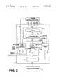
- FIG. 2is a block diagram showing an implementation of the invented graphics interface.
- FIG. 3ais a diagram showing the timing relationships between the signals pixel clock (PCLK), start serial clock (STSC) and display enable (DISPE).
- PCLKpixel clock
- STSCstart serial clock
- DISPEdisplay enable
- FIG. 3bis a diagram showing the timing relationships between the-signals pixel clock (PCLK), start serial clock (STSC) and start select MUX (STSOE).
- PCLKpixel clock
- STSCstart serial clock
- STSOEstart select MUX
- FIG. 3cis a diagram showing the timing relationships between the signals pixel clock (PCLK), start serial clock (STSC) and start shift load (STSRLD).
- PCLKpixel clock
- STSCstart serial clock
- STSRLDstart shift load
- FIG. 4is a diagram showing timing relationships between the signals PCLK, STSOE, SOE0, SOE1, SOE2 and SOE3.
- FIG. 5is a block diagram of data formatter and shift register 25.
- FIG. 6is a timing diagram showing the relationships between the various clocks and control signals utilized in the invention for flexible MUX logic 43 and data formatter 25 for a color mode having 16.7M colors and ratio of 16:3
- FIG. 1is a block overview showing a graphics display system in which the present invention may be utilized.
- the display systemcomprises a host processor with CPU 11, graphics display processor 13, video memory 15, graphics interface 17, RAMDAC 19 and display 21.
- the inventionlies in the graphics interface module which allows for 8, 16, 24 or 32 bit wide output on the data bus from the interface to RAMDAC 19.
- circuitry performing the function of graphics interface 17usually is able to output only one of 8, 16 or 32 bit wide output to the RAMDAC.
- some sophisticated graphics interfacesare capable of operating in a 24 bit wide mode, such prior an graphics interfaces require three graphics display processors, and three different sets of video memory to operate in 24 bit wide mode.
- a display system of the type in which the present invention may be utilizedplaces data generated by host processor 11, after processing by graphic displays processor 13, into a video memory 15.
- the display processorconstantly updates the video memory based upon the data generated by the host processor 11.
- the data in video memory 15is transferred to a graphics interface 17 which receives the data from the video memory and passes it to RAMDAC 19 which converts the digitized data into analog signals capable of being displayed by a display 21.
- the capabilities of the graphics interfaceare limited in that prior art graphics interfaces are capable of handling only a relatively small number of display modes as compared with the graphics interface of the present invention.
- FIG. 2is a block diagram of the elements of a graphics interface 17 according to the present invention.
- the interfacecomprises a flexible interleave multiplexor 41 utilizing flexible multiplexor logic 43 and a register 45, serial clock generator 23, data formatter and shift register 25, multiplexor control 27 and data pipeline 31.
- Video RAM 15 shown in FIG. 2is a standard video RAM, e.g. a 256K*4 or 256K*8 or 256K*16 VRAM which stores video information to be displayed on a display 21 (not shown in FIG. 2).
- the video RAMis connected to the graphics interface 17 by a 32, 64, 96 or 128-bit serial bus, depending on total video memory installed with FIG. 2 showing the connection by a 128-bit serial bus.
- One bank (1 MByte), two banks (2 MBytes), three banks (3 Mbytes) or four banks (4 Mbytes) of video RAMwill provide a 32, 64, 96, or 128-bit serial bus to graphics interface 17 respectively, the operation and implementation details of which are well known to persons skilled in the field of the invention.
- the inventionby virtue of the flexible interleave multiplexor 41, provides a flexible interleave scheme which provides support for the graphics modes shown in Table I which shows interleave ratio as a function of the maximum number of colors which can be simultaneously displayed versus the size of the serial bus.
- bits per pixel8 bitpp, 24 bitpp and 32 bitpp represent 256 colors, 32K/64K colors, 16 Million colors and 16 Million colors with alpha overlay respectively.
- prior art graphics interfacescan display 256, 32K/64K or 16.7M w/alpha colors at one time with 32 bit and 64 bit serial buses at the interleave ratios shown in Table I.
- the present inventionprovides a mechanism for utilizing 96 bit and 128 bit serial buses as well as for displaying 16.7M colors at 4:3, 8:3, 12:3 and 16:3 interleave ratios. In this manner, the present invention provides a more efficient use of video RAM since 16.7M colors can be displayed using a smaller interleave ratio than that which is required by prior an graphics interfaces.
- the inventionalso supports the resolutions and frequencies shown in Table II.
- the inputs to serial clock generator 23are the signals pixel clock (PCLK), start serial clock (STSC), and display enable (DISPE).
- Pixel clockis a clock signal generated by graphics processor 13 having a frequency of 32 MHz, 50 MHz, 85 MHz or 135 MHz depending on the resolution of the display being utilized as shown in Table II.
- the signal start serial clockis a signal generated by the graphics processor at a relative timing with respect to the display enable signal.
- the display enable (DISPE) signalis generated by the graphics processor when the video appears on the monitor.
- This DISPE signalis the composite of the vertical display enable and horizontal display enable signals. It is generated by a pair of counters and comparators. Basically, it tells the graphics interface when to display the first scanline and other scanlines and when to display pixels of each scanline. The specific details of its generation are well known to persons skilled in the art.
- Table III and FIG. 3adescribe the relationship between the signals start serial clock and display enable, i.e., the number of pixel clock cycles (Y) between the rising edge of the start serial clock and the rising edge of display enable (see FIG. 3a).
- Serial clock generator 23generates three clock signals, one of which (SC) is input to video RAM 15 and two of which (STSOE and STSRLD) are input to multiplexor control 27.
- the SC or shift clock signal input to video RAM 15is generated from the pixel clock signal as shown in Table IV.
- serial clock generator 23The two inputs to multiplexor control 27 from serial clock generator 23 are start shift load (STSRLD), and start select MUX (STSOE).
- the serial clock generator 23is a complex state machine used to generate the SC (shift clock) signal which is described in Table IV.
- SCshift clock
- the SC signalstarts to toggle when the serial clock generator 23 detects the STSC (start serial clock) signal.
- the SC signalcontinues as described in Table IV.
- the SC signalterminates when the falling edge of the DISPE (display enable) signal is detected.
- the serial clock generator 23also generates the STSOE and STSRLD signals.
- the STSOE signaltells multiplexor control 27 when to toggle the SOE0, SOE1, SOE2, SOE3 signals.
- the STSRLD signaltells multiplexor control 27 when to start loading data from flexible multiplexor 41 to data formatter and shift register 25. There is a relationship between the STSC and STSOE signals which is shown in FIG. 3b.
- Table V and FIG. 3bdescribe the relationship between the STSC and STSOE signals.
- Table VI and FIG. 3cdescribe the relationship between the STSC and STSRLD signals.
- Multiplexor control 27generates shift load (SRLD) and pixel count (PXCNT) ⁇ 3:0> which are input to data formatter and shift register 25. Details regarding the generation of the SRLD and PXCNT signals are set forth below.
- the signal inputs to flexible interleave multiplexor 41 from multiplexor control 27are SOE0, SOE1, SOE2 and SOE3 designated as SOE ⁇ 3:0>.
- the SOE ⁇ 3:0> signalsare mutually exclusive.
- SOE0, SOE1, SOE2, SOE3are generated from STSOE. SOE0, SOE1, SOE2, and SOE3 and select 32-bit data from VRAM 15 bank 0, 1, 2, and 3 respectively.
- the SOE0, SOE1, SOE2, and SOE3 signalsare very complicated, especially in 24 bit-per-pixel mode.
- SOE ⁇ 3:0>is asserted every 4 clocks alternately.
- the signals SOE0, SOE1, SOE2 and SOE3have the timings shown in FIG. 4 relative to the PCLK and STSOE signals.
- each SOE signalThere are typically more than 12 different waveforms for each SOE signal, because the invention supports 4 banks, and each bank supports 4 modes (8,16,24 and 32 bit-per-pixel).
- An implementation of the inventionalso supports 4 bit-per-pixel mode, but since the details of such implementation are not needed for an understanding of the invention, and should be readily apparent to persons skilled in the art, the specific details of such implementation are not set forth herein.
- Tables VII, VIII, IX and Xdescribe how the SOE0 signal is generated from the STSOE signal and how the SOE0, SOE1, SOE2 and SOE3 signals relate to each other.
- Data pipeline 31operates as a data buffer to RAMDAC 19 and may be implemented as a 32-bit register.
- serial clock generator 23inputs to serial clock generator 23 are pixel clock (PCLK), start serial clock (STSC) and display enable (DISPE).
- PCLKpixel clock
- STSCstart serial clock
- DISPEdisplay enable
- Multiplexor control 27generates the 4-bit pixel count (PXCNT ⁇ 3:0>) as one input to data formatter and shift register 25. Pixel count is generated in the 24 bit-per-pixel mode only. A circular counter is used to generate these 4 signals counting 1, 2, 4, 8 then repeating from 1 each PCLK. The circular counter is reset when it is not in 24 bit-per-pixel mode or when the display enable signal is inactive.
- Multiplexor control 27also generates the shift and register load control signal (SRLD) as another input to data formatter and shift register 25.
- SRLDshift and register load control signal
- the signal SRLDis generated as shown in Table XI.
- Multiplexor control 27also generates the four bit serial output enable (SOE ⁇ 3:0>) signal which is input to flexible MUX logic 43.
- SOE ⁇ 3:0> signalsA detailed description of the SOE ⁇ 3:0> signals has been described above with reference to Tables VII-X.
- serial clock generatorgenerates the shift clock (SC) signal which is used to control the loading of register 45 from video RAM 15.
- SCshift clock
- Flexible MUX logic 43receives 128 bit wide data from register 45 and selects one of four 32 bit wide pieces of data corresponding to one of four 32 bit wide pieces of data from bank 1 to bank 4 of video RAM 15 depending on the value of SOE which cycles between 0, 1, 2 and 3 as noted above to select a corresponding one of the 32 bit wide pieces of data.
- Shift register 51receives 32 bit data from flexible MUX logic 43. This data is passed to another register 53 and logic 55 each PCLK. Logic 55 operates on the data from register 51 and register 53, which are delayed by one PCLK, and PXCNT ⁇ 3:0> as follows.
- logic 55may be implemented so that it performs the following logic operations:
- FIG. 6is a timing diagram showing the relationships between the various clocks and control signals utilized in the invention for flexible MUX logic 43 and data formatter 25 for a color mode having 16.7M colors and ratio of 16:3 in 4 bank, 24-bit per pixel mode.
- the pixel clock PCLK, the shift clock SC, the SOE0, SOE1, SOE2, and SOE3 signalsare used to select 32-bit source, data A from flexible MUX logic 43, data B from shift register 51 delayed by one PCLK from data A, data B' from register 53 delayed by one PCLK from data B', and finally data C output from logic 55 as a function of pixel count.
- the data from VRAM bank 0are identified within data A, data B, data B' and data C in FIG. 6 from the least significant byte to the most significant byte as 0, 1, 2, and 3 respectively.
- the data from VRAM bank 1are identified from the least significant byte to the most significant byte as 4, 5, 6, and 7 respectively.
- the data from VRAM bank 2are identified from the least significant byte to the most significant byte as 8, 9, 10, and 11 respectively.
- the data from VRAM bank 3are identified from the least significant byte to the most significant byte as 12, 13, 14, and 15, respectively.
- the inventionalso provides a mechanism to allow data from the VRAM to be selected from any one of four banks by using the signal SOEBANKSEL ⁇ 1:0> as shown in FIG. 2.
- This signalutilizes the least significant two bits of the current scan line address generated by the graphics processor and causes the VRAM banks to be selected as follows.
- VRAMhas only one bank installed, then data is fetched from that bank regardless of the value of SOEBANKSEL ⁇ 1> and SOEBANKSEL ⁇ 0>.
Landscapes
- Engineering & Computer Science (AREA)
- Physics & Mathematics (AREA)
- Computer Hardware Design (AREA)
- General Physics & Mathematics (AREA)
- Theoretical Computer Science (AREA)
- Controls And Circuits For Display Device (AREA)
Abstract
Description
TABLE I ______________________________________ INTERLEAVE RATIO TABLE MAX. NO. OF COLORS DISPLAYED AT A GIVEN TIME SERIAL BUS 256 32K/64K 16.7M 16.7M w/alpha ______________________________________ 32-bit (4 bytes) 4:1 4:2 4:3 4:4 64-bit (8 bytes) 8:1 8:2 8:3 8:4 96-bit (12 bytes) 12:1 12:2 12:3 12:4 128-bit (16 bytes) 16:1 16:2 16:3 16:4 ______________________________________
TABLE II ______________________________________ Vertical. Resolution No. of Bits per Pixel Pixel Clock Ref. Clock ______________________________________ 640×480 8 32 MHz 73 Hz 640×480 16 32 MHz 73 Hz 640×480 24 32 MHz 73 Hz 640×480 32 32 MHz 73 Hz 800×600 8, 16, 24, 32 50 MHz 73 Hz 1024×768 8, 16, 24, 32 85 MHz 73 Hz 1280×1024 8, 16, 24, 32 135 MHz 73 Hz ______________________________________
TABLE III ______________________________________ Bank No. No. of Bits per Pixel Y (in terms of pixel clocks) ______________________________________ 1 8 9 1 16 5 1 24 3 1 32 3 2 8 13 2 16 7 2 24 4 2 32 4 3 8 17 3 16 9 3 24 6 3 32 5 4 8 21 4 16 11 4 24 6 4 32 6 ______________________________________
TABLE IV ______________________________________ No. of No. of SC (shift clock) banks Bits per Pixel derived from PCLK (pixel clock) ______________________________________ 1 8 2 PCLK high, 2 PCLK low, then repeat 1 16 1 PCLK high, 1 PCLK low, then repeat 1 24 0.5 PCLK high, 0.5 PCLK low, 0.5 PCLK high, 0.5 PCLK low, 0.5 PCLK high, 1.5 PCLK low, then repeat 1 32 same as PCLK 2 8 4 PCLK high, 4 PCLK low, then repeat 2 16 2 PCLK high, 2 PCLK low, then repeat 2 24 1 PCLK high, 1 PCLK low, 1 PCLK high, 2 PCLK low, 1 PCLK high, 2 PCLK low then repeat 2 32 1 PCLK high, 1 PCLK low, then repeat 3 8 6 PCLK high, 6 PCLK low, then repeat 3 16 3 PCLK high, 3 PCLK low, then repeat 3 24 2 PCLK high, 2 PCLK low, then repeat 3 32 1 PCLK high, 2 PCLK low, then repeat 4 8 8 PCLK high, 8 PCLK low, then repeat 4 16 4 PCLK high, 4 PCLK low, then repeat 4 24 2 PCLK high, 3 PCLK low, 2 PCLK high, 3 PCLK low, 3 PCLK high, 3 PCLK low, then repeat 4 32 2 PCLK high, 2 PCLK low, then repeat ______________________________________
TABLE V ______________________________________ Bank No. No. of Bits per Pixel X (in terms of pixel clocks) ______________________________________ 1 8 01 1 16 01 1 24 01 1 32 01 2 8 8 2 16 4 2 24 2 2 32 2 3 8 12 3 16 6 3 24 4 3 32 3 4 8 16 4 16 8 4 24 4 4 32 4 ______________________________________
TABLE VI ______________________________________ Bank No. No. of Bits per Pixel W (in terms of pixel clocks) ______________________________________ 1 8 7 1 16 3 1 24 1 1 32 1 2 8 11 2 16 5 2 24 2 2 32 2 3 8 15 3 16 7 3 24 4 3 32 3 4 8 19 4 16 9 4 24 4 4 32 4 ______________________________________
TABLE VII ______________________________________ No. of No. of Banks Bits per Pixel SOE0 Derived from STSOE ______________________________________ 1 8 always high 1 16 always high 1 24 always high 1 32 always high 2 8 4 PCLK high, 4 PCLK low, then repeat 2 16 2 PCLK high, 2 PCLK low, then repeat 2 24 1 PCLK high, 1 PCLK low, 1 PCLK high, 2 PCLK low, 1 PCLK high, 2 PCLK low thenrepeat 2 32 1 PCLK high, 1 PCLK low, then repeat 3 8 3 PCLK high, 9 PCLK low, then repeat 3 16 2 PCLK high, 4 PCLK low, then repeat 3 24 1 PCLK high, 3 PCLK low, then repeat 3 32 1 PCLK high, 2 PCLK low, then repeat 4 8 4 PCLK high, 12 PCLK low, then repeat 4 16 2 PCLK high, 6 PCLK low, then repeat 4 24 1 PCLK high, 4 PCLK low, 1 PCLK high, 4 PCLK low, 1 PCLK high, 5 PCLK low, then repeat 4 32 1 PCLK high, 3 PCLK low, then repeat ______________________________________
TABLE VIII ______________________________________ No. of No. of Banks Bits per Pixel SOE1 derived from SOE0 ______________________________________ 1 8 always low 1 16 always low 1 24 always low 1 32 always low 2 8 4 PCLK high, 4 PCLK low, then repeat 2 16 2 PCLK high, 2 PCLK low, then repeat 2 24 1 PCLK high, 1 PCLK low, 2 PCLK high, 1 PCLK low, 2 PCLK high, 1 PCLK low thenrepeat 2 32 1 PCLK high, 1 PCLK low, then repeat 3 8 3 PCLK high, 9 PCLK low, then repeat 3 16 2 PCLK high, 4 PCLK low, then repeat 3 24 1 PCLK high, 3 PCLK low, then repeat 3 32 1 PCLK high, 2 PCLK low, then repeat 4 8 4 PCLK high, 12 PCLK low, then repeat 4 16 2 PCLK high, 6 PCLK low, then repeat 4 24 1 PCLK high, 4 PCLK low, 2 PCLK high, 3 PCLK low, 2 PCLK high, 4 PCLK low, then repeat 4 32 1 PCLK high, 3 PCLK low, then repeat ______________________________________
TABLE IX ______________________________________ No. of No. of Banks Bits per Pixel SOE2 derived from SOE1 ______________________________________ 1 8 always low 1 16 always low 1 24 always low 1 32 always low 2 8 always low 2 16 always low 2 24 always low 2 32 always low 3 8 3 PCLK high, 9 PCLK low, then repeat 3 16 2 PCLK high, 4 PCLK low, then repeat 3 24 2 PCLK high, 2 PCLK low, then repeat 3 32 1 PCLK high, 2 PCLK low, then repeat 4 8 4 PCLK high, 12 PCLK low, then repeat 4 16 2 PCLK high, 6 PCLK low, then repeat 4 24 2 PCLK high, 4 PCLK low, 1 PCLK high, 4 PCLK low, 2 PCLK high, 3 PCLK low, then repeat 4 32 1 PCLK high, 3 PCLK low, then repeat ______________________________________
TABLE X ______________________________________ No. of No. of Banks Bits per Pixel SOE3 derived from SOE2 ______________________________________ 1 8 always low 1 16 always low 1 24 always low 1 32 always low 2 8 always low 2 16 always low 2 24 always low 2 32 always low 3 8 always low 3 16 always low 3 24 always low 3 32 always low 4 8 4 PCLK high, 12 PCLK low, then repeat 4 16 2 PCLK high, 6 PCLK low, then repeat 4 24 2 PCLK high, 4 PCLK low, 1 PCLK high, 4 PCLK low, 2 PCLK high, 3 PCLK low, then repeat 4 32 1 PCLK high, 3 PCLK low, then repeat ______________________________________
TABLE XI ______________________________________ No. of Bits per Pixel SRLD ______________________________________ 8 1 PCLK, 3 PCLK low, then repeat 16 1 PCLK high, 1 PCLK low, then repeat 24 always high 32 always high ______________________________________
C<31:0>=B<31:0>
______________________________________ C<31:24> = 0; C<23:16> = (B<23:16> AND PXCNT<0>) OR (B<15:8> AND PXCNT<1>) OR (B<7:0> AND PXCNT<2>) OR (B'<31:24> AND PXCNT<3>); C<15:8> = (B<15:8> AND PXCNT<0>) OR (B<7:0> AND PXCNT<1>) OR (B'<31:24> AND PXCNT<2>) OR (B'<23:16> AND PXCNT<3>); C<7:0> = (B<7:0> AND PXCNT<0>) OR (B'<31:24> AND PXCNT<1>) OR (B'<23:16> AND PXCNT<2>) OR (B'<15:8> AND PXCNT<3>). ______________________________________
______________________________________ First SOEBANKSEL<1> SOEBANKSEL<0> Bank Selected ______________________________________ 0 0Bank 0 0 1Bank 1 1 0Bank 0 1 1Bank 1 ______________________________________
______________________________________ First SOEBANKSEL<1> SOEBANKSEL<0> Bank Selected ______________________________________ 0 0Bank 0 0 1Bank 1 1 0Bank 2 1 1 undefined ______________________________________
______________________________________ First SOEBANKSEL<1> SOEBANKSEL<0> Bank Selected ______________________________________ 0 0Bank 0 0 1Bank 1 1 0Bank 2 1 1Bank 3 ______________________________________
Claims (9)
Priority Applications (1)
| Application Number | Priority Date | Filing Date | Title |
|---|---|---|---|
| US08/205,887US5436641A (en) | 1994-03-03 | 1994-03-03 | Flexible graphics interface for multiple display modes |
Applications Claiming Priority (1)
| Application Number | Priority Date | Filing Date | Title |
|---|---|---|---|
| US08/205,887US5436641A (en) | 1994-03-03 | 1994-03-03 | Flexible graphics interface for multiple display modes |
Publications (1)
| Publication Number | Publication Date |
|---|---|
| US5436641Atrue US5436641A (en) | 1995-07-25 |
Family
ID=22764061
Family Applications (1)
| Application Number | Title | Priority Date | Filing Date |
|---|---|---|---|
| US08/205,887Expired - Fee RelatedUS5436641A (en) | 1994-03-03 | 1994-03-03 | Flexible graphics interface for multiple display modes |
Country Status (1)
| Country | Link |
|---|---|
| US (1) | US5436641A (en) |
Cited By (8)
| Publication number | Priority date | Publication date | Assignee | Title |
|---|---|---|---|---|
| US5519438A (en)* | 1994-06-30 | 1996-05-21 | Intel Corporation | Computer with a video subsystem that contains timers which are used to create calibration tables correlating time intervals with the decoding and converting of video input signals |
| EP0734008A1 (en)* | 1995-03-21 | 1996-09-25 | Sun Microsystems, Inc. | Time multiplexing of pixel data out of a video frame buffer |
| US5642139A (en)* | 1994-04-29 | 1997-06-24 | Cirrus Logic, Inc. | PCMCIA video card |
| US5828384A (en)* | 1995-09-14 | 1998-10-27 | Ricoh Company, Ltd. | Image display control device, method and computer program product |
| US6313880B1 (en) | 1997-04-03 | 2001-11-06 | Sony Corporation | Display with one or more display windows and placement dependent cursor and function control |
| US6501441B1 (en) | 1998-06-18 | 2002-12-31 | Sony Corporation | Method of and apparatus for partitioning, scaling and displaying video and/or graphics across several display devices |
| US6593937B2 (en) | 1998-06-18 | 2003-07-15 | Sony Corporation | Method of and apparatus for handling high bandwidth on-screen-display graphics data over a distributed IEEE 1394 network utilizing an isochronous data transmission format |
| US20070035668A1 (en)* | 2005-08-11 | 2007-02-15 | Sony Corporation | Method of routing an audio/video signal from a television's internal tuner to a remote device |
Citations (8)
| Publication number | Priority date | Publication date | Assignee | Title |
|---|---|---|---|---|
| US5027212A (en)* | 1989-12-06 | 1991-06-25 | Videologic Limited | Computer based video/graphics display system |
| US5083119A (en)* | 1988-02-11 | 1992-01-21 | Du Pont Pixel Systems Limited | State machine controlled video processor |
| US5115314A (en)* | 1990-04-26 | 1992-05-19 | Ross Video Limited | Video keying circuitry incorporating time division multiplexing |
| US5150109A (en)* | 1989-02-13 | 1992-09-22 | Touchstone Computers, Inc. | VGA controller card |
| US5206833A (en)* | 1988-09-12 | 1993-04-27 | Acer Incorporated | Pipelined dual port RAM |
| US5227863A (en)* | 1989-11-14 | 1993-07-13 | Intelligent Resources Integrated Systems, Inc. | Programmable digital video processing system |
| US5257237A (en)* | 1989-05-16 | 1993-10-26 | International Business Machines Corporation | SAM data selection on dual-ported DRAM devices |
| US5289565A (en)* | 1990-07-09 | 1994-02-22 | Rasterops Corporation | Methods and apparatus for CYMK-RGB RAMDAC |
- 1994
- 1994-03-03USUS08/205,887patent/US5436641A/ennot_activeExpired - Fee Related
Patent Citations (8)
| Publication number | Priority date | Publication date | Assignee | Title |
|---|---|---|---|---|
| US5083119A (en)* | 1988-02-11 | 1992-01-21 | Du Pont Pixel Systems Limited | State machine controlled video processor |
| US5206833A (en)* | 1988-09-12 | 1993-04-27 | Acer Incorporated | Pipelined dual port RAM |
| US5150109A (en)* | 1989-02-13 | 1992-09-22 | Touchstone Computers, Inc. | VGA controller card |
| US5257237A (en)* | 1989-05-16 | 1993-10-26 | International Business Machines Corporation | SAM data selection on dual-ported DRAM devices |
| US5227863A (en)* | 1989-11-14 | 1993-07-13 | Intelligent Resources Integrated Systems, Inc. | Programmable digital video processing system |
| US5027212A (en)* | 1989-12-06 | 1991-06-25 | Videologic Limited | Computer based video/graphics display system |
| US5115314A (en)* | 1990-04-26 | 1992-05-19 | Ross Video Limited | Video keying circuitry incorporating time division multiplexing |
| US5289565A (en)* | 1990-07-09 | 1994-02-22 | Rasterops Corporation | Methods and apparatus for CYMK-RGB RAMDAC |
Cited By (11)
| Publication number | Priority date | Publication date | Assignee | Title |
|---|---|---|---|---|
| US5642139A (en)* | 1994-04-29 | 1997-06-24 | Cirrus Logic, Inc. | PCMCIA video card |
| US6023266A (en)* | 1994-04-29 | 2000-02-08 | Cirrus Logic, Inc. | PCMCIA video card |
| US5519438A (en)* | 1994-06-30 | 1996-05-21 | Intel Corporation | Computer with a video subsystem that contains timers which are used to create calibration tables correlating time intervals with the decoding and converting of video input signals |
| EP0734008A1 (en)* | 1995-03-21 | 1996-09-25 | Sun Microsystems, Inc. | Time multiplexing of pixel data out of a video frame buffer |
| US5696534A (en)* | 1995-03-21 | 1997-12-09 | Sun Microsystems Inc. | Time multiplexing pixel frame buffer video output |
| US5828384A (en)* | 1995-09-14 | 1998-10-27 | Ricoh Company, Ltd. | Image display control device, method and computer program product |
| US6313880B1 (en) | 1997-04-03 | 2001-11-06 | Sony Corporation | Display with one or more display windows and placement dependent cursor and function control |
| US6501441B1 (en) | 1998-06-18 | 2002-12-31 | Sony Corporation | Method of and apparatus for partitioning, scaling and displaying video and/or graphics across several display devices |
| US6593937B2 (en) | 1998-06-18 | 2003-07-15 | Sony Corporation | Method of and apparatus for handling high bandwidth on-screen-display graphics data over a distributed IEEE 1394 network utilizing an isochronous data transmission format |
| US7075557B2 (en) | 1998-06-18 | 2006-07-11 | Sony Corporation | Method of and apparatus for handling high bandwidth on-screen-display graphics data over a distributed IEEE 1394 network utilizing an isochronous data transmission format |
| US20070035668A1 (en)* | 2005-08-11 | 2007-02-15 | Sony Corporation | Method of routing an audio/video signal from a television's internal tuner to a remote device |
Similar Documents
| Publication | Publication Date | Title |
|---|---|---|
| US4823120A (en) | Enhanced video graphics controller | |
| US5402148A (en) | Multi-resolution video apparatus and method for displaying biological data | |
| US4490797A (en) | Method and apparatus for controlling the display of a computer generated raster graphic system | |
| US5400057A (en) | Internal test circuits for color palette device | |
| US5481319A (en) | Motion detection method and apparatus | |
| US5473342A (en) | Method and apparatus for on-the-fly multiple display mode switching in high-resolution bitmapped graphics system | |
| US20090213110A1 (en) | Image mixing apparatus and pixel mixer | |
| JPH05204373A (en) | High precision multimedia-display | |
| JPS59186A (en) | Color signal generator for raster scan type video display | |
| KR970703568A (en) | METHOD AND APPARATUS FOR IMAGE POTATION | |
| KR950003981B1 (en) | Display Control Unit for Flat Displays | |
| AU602062B2 (en) | Video apparatus employing vrams | |
| GB2076187A (en) | Microcomputer apparatus with video display capability | |
| US5086295A (en) | Apparatus for increasing color and spatial resolutions of a raster graphics system | |
| US5436641A (en) | Flexible graphics interface for multiple display modes | |
| EP0051655A4 (en) | Apparatus for the display and storage of television picture information by using a memory accessible from a computer. | |
| CA1292335C (en) | Raster scan digital display system | |
| US5559532A (en) | Method and apparatus for parallel pixel hardware cursor | |
| US5473341A (en) | Display control apparatus | |
| JPH04305160A (en) | Trigger generation method using buffer memory | |
| US4901062A (en) | Raster scan digital display system | |
| EP0465102A2 (en) | Palette devices selection of multiple pixel depths packing the entire width of the bus | |
| GB2234094A (en) | Dual-mode video board with parallel-to-serial conversion | |
| KR100448939B1 (en) | Resolution transform circuit of liquid crystal display device, especially implementing multi-synch | |
| KR100213003B1 (en) | Character magnifier |
Legal Events
| Date | Code | Title | Description |
|---|---|---|---|
| AS | Assignment | Owner name:CIRRUS LOGIC, INC., CALIFORNIA Free format text:ASSIGNMENT OF ASSIGNORS INTEREST;ASSIGNORS:HOANG, THUAN THAI;KAPUR, RAJAN NETRALAL;CHUE, WILLIAM W.Y.;REEL/FRAME:006913/0456 Effective date:19940222 | |
| AS | Assignment | Owner name:BANK OF AMERICA NATIONAL TRUST & SAVINGS ASSOCIATI Free format text:SECURITY INTEREST;ASSIGNOR:CIRRUS LOGIC, INC.;REEL/FRAME:007986/0917 Effective date:19960430 | |
| FEPP | Fee payment procedure | Free format text:PAYOR NUMBER ASSIGNED (ORIGINAL EVENT CODE: ASPN); ENTITY STATUS OF PATENT OWNER: LARGE ENTITY | |
| FPAY | Fee payment | Year of fee payment:4 | |
| REMI | Maintenance fee reminder mailed | ||
| AS | Assignment | Owner name:CIRRUS LOGIC INTERNATIONAL LTD., BERMUDA Free format text:DEED OF DISCHARGE;ASSIGNOR:BANK OF AMERICA NATIONAL TRUST SAVINGS ASSOCIATION;REEL/FRAME:013782/0435 Effective date:19970630 | |
| LAPS | Lapse for failure to pay maintenance fees | ||
| LAPS | Lapse for failure to pay maintenance fees | Free format text:PATENT EXPIRED FOR FAILURE TO PAY MAINTENANCE FEES (ORIGINAL EVENT CODE: EXP.); ENTITY STATUS OF PATENT OWNER: LARGE ENTITY | |
| STCH | Information on status: patent discontinuation | Free format text:PATENT EXPIRED DUE TO NONPAYMENT OF MAINTENANCE FEES UNDER 37 CFR 1.362 | |
| FP | Lapsed due to failure to pay maintenance fee | Effective date:20030725 | |
| AS | Assignment | Owner name:NVIDIA INTERNATIONAL, INC., BARBADOS Free format text:ASSIGNMENT OF ASSIGNORS INTEREST;ASSIGNOR:CIRRUS LOGIC, INC.;REEL/FRAME:014646/0167 Effective date:20030813 Owner name:NVIDIA INTERNATIONAL, INC. C/0 PRICEWATERHOUSECOOP Free format text:ASSIGNMENT OF ASSIGNORS INTEREST;ASSIGNOR:CIRRUS LOGIC, INC.;REEL/FRAME:014646/0167 Effective date:20030813 | |
| AS | Assignment | Owner name:NVIDIA CORPORATION, CALIFORNIA Free format text:ASSIGNMENT OF ASSIGNORS INTEREST;ASSIGNOR:NVIDIA INTERNATIONAL INC.;REEL/FRAME:029418/0249 Effective date:20121203 |