US5436189A - Self-aligned channel stop for trench-isolated island - Google Patents
Self-aligned channel stop for trench-isolated islandDownload PDFInfo
- Publication number
- US5436189A US5436189AUS08/106,160US10616093AUS5436189AUS 5436189 AUS5436189 AUS 5436189AUS 10616093 AUS10616093 AUS 10616093AUS 5436189 AUS5436189 AUS 5436189A
- Authority
- US
- United States
- Prior art keywords
- semiconductor
- trench
- layer
- semiconductor layer
- conductivity type
- Prior art date
- Legal status (The legal status is an assumption and is not a legal conclusion. Google has not performed a legal analysis and makes no representation as to the accuracy of the status listed.)
- Expired - Lifetime
Links
Images


Classifications
- H—ELECTRICITY
- H01—ELECTRIC ELEMENTS
- H01L—SEMICONDUCTOR DEVICES NOT COVERED BY CLASS H10
- H01L21/00—Processes or apparatus adapted for the manufacture or treatment of semiconductor or solid state devices or of parts thereof
- H01L21/70—Manufacture or treatment of devices consisting of a plurality of solid state components formed in or on a common substrate or of parts thereof; Manufacture of integrated circuit devices or of parts thereof
- H01L21/71—Manufacture of specific parts of devices defined in group H01L21/70
- H01L21/76—Making of isolation regions between components
- H01L21/763—Polycrystalline semiconductor regions
- H—ELECTRICITY
- H01—ELECTRIC ELEMENTS
- H01L—SEMICONDUCTOR DEVICES NOT COVERED BY CLASS H10
- H01L21/00—Processes or apparatus adapted for the manufacture or treatment of semiconductor or solid state devices or of parts thereof
- H01L21/70—Manufacture or treatment of devices consisting of a plurality of solid state components formed in or on a common substrate or of parts thereof; Manufacture of integrated circuit devices or of parts thereof
- H01L21/71—Manufacture of specific parts of devices defined in group H01L21/70
- H01L21/76—Making of isolation regions between components
- H01L21/762—Dielectric regions, e.g. EPIC dielectric isolation, LOCOS; Trench refilling techniques, SOI technology, use of channel stoppers
- Y—GENERAL TAGGING OF NEW TECHNOLOGICAL DEVELOPMENTS; GENERAL TAGGING OF CROSS-SECTIONAL TECHNOLOGIES SPANNING OVER SEVERAL SECTIONS OF THE IPC; TECHNICAL SUBJECTS COVERED BY FORMER USPC CROSS-REFERENCE ART COLLECTIONS [XRACs] AND DIGESTS
- Y10—TECHNICAL SUBJECTS COVERED BY FORMER USPC
- Y10S—TECHNICAL SUBJECTS COVERED BY FORMER USPC CROSS-REFERENCE ART COLLECTIONS [XRACs] AND DIGESTS
- Y10S148/00—Metal treatment
- Y10S148/05—Etch and refill
Definitions
- the present inventionrelates in general to trench-isolated semiconductor devices and is particularly directed to a mechanism for forming a channel stop that is self-aligned with the trench walls.
- trench isolationis often used to isolate semiconductor islands within an integrated circuit architecture.
- trench isolationis also commonly employed with PN junction isolation of the bottom or floor of the island, as diagrammatically illustrated in FIG. 1, which shows an N- island 11 atop an support substrate 12.
- the sides of island 11are isolated by means of a trench 13, typically filled with an insulator (oxide) layer 14 and conductor (polysilicon) material.
- trench isolation technologyAs trench isolation technology has developed it has been increasingly used to isolate thicker islands, such as those employed for high voltage (e.g. in excess of 30 volts) devices. With the relatively large field gradients in such-devices there is the possibility of the formation of a parasitic inversion path 17 beneath the surface oxide layer 18 and along the sidewall of the island 11, which electrically connects a device region, such as P type diffusion region 21 formed in the surface of island 11, with the underlying substrate.
- Such a parasitic pathmay be caused, for example, by the gating action of the potential applied to polysilicon material 15 together with the voltage of an interconnect line (not shown) which overlies surface oxide layer 18 between region 21 and trench 13, by the action of negative charge on and/or in the surface and sidewall oxide layers, or by a combination of charge and gate bias.
- High voltage-islandsare particularly prone to the problem since they use higher resistivity material, which has a lower inversion threshold voltage than lower resistivity material, to achieve a higher breakdown voltage.
- the higher voltages present on the conductorscause the parasitic devices to turn on.
- a channel stopwhich, for a high voltage junction, typically takes the form of a diffusion, such as diffusion region 31 shown in FIG. 2, having the same conductivity type as island 11, surrounding the opposite conductivity diffusion 21.
- the surface concentration of the channel stopis elevated with respect to that of the island and is made high enough so that it does not invert under worst case conditions.
- the channel stop regionis spaced apart from region 21, which increases device occupation area and thus reduces integration density.
- the need to provide a separation region between the trench and a device region within the island, which results in an unwanted increase in occupation areais obviated by channel stop formation technique through which the stop is self-aligned with the trench sidewall, so that there is no alignment tolerance between the stop and the trench wall.
- the width of the stopis controlled by lateral diffusion, which can be smaller than the width of a line defined by a mask, since that width is the minimum mask width plus twice the lateral diffusion of the layer defined by the mask.
- an initial masking layere.g. oxide, through which the trench pattern is to be formed in the semiconductor island layer, is used as a doping mask for introducing a channel stop dopant into a surface portion of the semiconductor layer where the trench is to be formed.
- the lateral diffusion of the dopant beneath the oxide and adjacent to the trench aperturedefines the eventual size of the channel stop, such that its lateral dimension is less than its depth, or vertical dimension, since an inherent characteristic of such lateral diffusion is that the dimension of the lateral diffusion beneath the mask is less than the diffusion depth into the semiconductor layer exposed by the mask aperture.
- the semiconductor layeris then anisotropically etched to form a trench to a prescribed depth, usually intersecting the underlying semiconductor substrate.
- the channel stopis self-aligned with the sidewall of the trench.
- the trenchmay be then oxidized and filled with polysilicon material to complete the trench isolation process.
- FIG. 1diagrammatically illustrates PN junction isolation at the bottom of a conventional trench-isolated island
- FIG. 2illustrates a conventional channel stop mechanism for circumventing inversion for a high voltage junction in a trench-isolated island
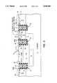
- FIGS. 3a-3ddiagrammatically illustrate a trench-isolated semiconductor device employing a self-aligned channel stop, in cross-section, at respective stages of the manufacturing process of the present invention
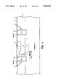
- FIG. 4shows a completed trench-isolated island structure having an underlying N+ region and a pair of channel stop regions that are contiguous with the sidewalls of isolation trenches;
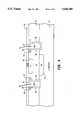
- FIG. 5is a cross-sectional side view of an arrangement of P and N islands trench-isolated on an underlying P substrate having self-aligned channel stop regions;
- FIG. 6is a top view of the arrangement of P and N islands trench-isolated on an underlying P substrate having self-aligned channel stop regions as shown in FIG. 5.
- FIGS. 3a-3da trench-isolated semiconductor device employing a self-aligned channel stop is diagrammatically illustrated, in cross-section, at respective stages of manufacture.
- FIG. 3ashows a semiconductor (e.g. silicon) substrate 41 of a first conductivity type (e.g. P type), having a semiconductor layer 43 of a second conductivity type (e.g. N- type), formed on substrate 41 and having a top surface 45.
- a semiconductore.g. silicon
- a first conductivity typee.g. P type
- a semiconductor layer 43 of a second conductivity typee.g. N- type
- an insulator layer 49such as silicon oxide, which is selectively patterned to form one or more apertures 51, exposing respective surface portions 53 of the semiconductor layer 43 for the purpose of defining an etch mask which will delineate the trench-isolated island.
- a channel stop dopantan N type impurity such as phosphorous
- a channel stop dopantis introduced (diffused) into semiconductor layer 43 through aperture 51 in insulator layer 49, so as to form a high impurity concentration region 55, which will serve as the source of channel stop regions and extends into the adjacent surface of semiconductor layer 43 beneath insulator layer 49, as shown in FIG. 3b.
- Region 55has an impurity concentration greater (N) than that (N-) of semiconductor layer 43, and is sufficiently high that it does not invert under worst case conditions.
- a trench 54is formed in semiconductor layer 43 through aperture 51 and region 55.
- semiconductor layer 43is anisotropically etched, for example by a reactive ion etch, down to the substrate 41, as shown in FIG. 3c. Since the trench passes through the channel stop region, leaving region segments 57 and 59 that have diffused into surface regions of layer 43 adjacent to aperture 51, the sidewalls of regions 57 and 59 are inherently self-aligned with the sidewalls 56, 58 of the trench.
- channel stop regions 57 and 59are contiguous with both the top surface 45 and the trench sidewall surfaces 56, 58, having a width set (which is less than its depth, as described above) by lateral diffusion beneath oxide layer 49 so as to occupy minimum area.
- the sidewalls 56, 58 and floor, or bottom 60, of the trenchare coated or filled with an insulator layer 61, such as silicon oxide.
- an insulator layer 61such as silicon oxide.
- the trenchmay be followed by a layer of conductive material, for example by filling the oxide-coated trench with doped polysilicon 63, up to the surface of semiconductor layer 43.
- the original mask layermay then be stripped off surface 45, for subsequent processing.
- a region 47 of P conductivity typerepresentative of one or more semiconductor regions that define PN junctions with semiconductor layer 43 and form device regions of one or more prescribed circuit elements that make up the integrated circuit architecture. Region 47 may be formed by conventional processing subsequent to the trench refill.
- FIG. 4shows a completed trench-isolated island structure (P substrate 41/N- top layer 43) (absent contacts) having an N+ region 65, underlying P-type region 50 and a pair of channel stop regions 57 and 67 that are contiguous with the sidewalls 56, 58 and 66, 68 of respective trenches 54 and 64 but are spaced-apart from P-type region 50.
- Trenches 54 and 64contain a sidewall-contiguous layer of dielectric (oxide) 61, 61' and polysilicon refill 63, 63', respectively.
- the top surface 45 of semiconductor layer 43is covered with a thick field oxide 69, to minimize breakdown reduction, which may occur when a biased conductor lies over an N to N-high low junction.
- the manner of forming channel stop regions in accordance with the present inventioncreates no steps in the surface oxide layer. This absence of steps allows higher resolution lithography to be used and improves interconnect step coverage.
- FIGS. 5 and 6diagrammatically illustrate the application of the present invention to the case where complementary conductivity type islands (both P and N type) are trench-isolated within the same semiconductor wafer. More particularly.
- FIG. 5is a cross-sectional side view and FIG. 6 is a top view of an arrangement of P and N islands trench-isolated on an underlying P substrate 71, which contains a buried N separation layer 73 where the P island is to be formed.
- Manufacture of the illustrated complementary trench-isolated structureis initiated by providing a semiconductor substrate 71 (P type in the present example), in which N type isolation region 73 has been diffused where a surface P type island is to be formed.
- a shallow P type surface diffusionis formed in region 73 to serve a source of P dopant impurities during subsequent epitaxial formation of a top (N-) semiconductor layer 75.
- these P type impuritiesdiffuse up into layer 75 to form P type region 77.
- an additional P type region 79is selectively down-diffused through the top surface 81 of layer 75, so as to intersect region 77 and thereby define a P type island region 83 that is isolated from P type substrate by separation region 73.
- an alternative approachwould be to omit the preliminary formation of up diffusion region 77 and use only a down-diffusion to complete the island 83. Both techniques are conventional.
- epitaxial layer 75contains both N- and P type material that are to be trench-isolated both N and P type channel stop regions are to be formed.
- the self-alignment mechanism described above with reference to FIGS. 3a-3dis carried out for both island types.
- an extra oversize maskan ion-implant photoresist mask
- the P channel stop regionsare patterned in a similar manner. In the structure illustrated in FIG.
- P type channel stop regions 86 and 87, within P type island 83,are self-aligned with respective sidewalls 88 and 89 of trenches 91 and 92, while the opposite sidewalls of trenches 91 and 92 are contiguous with N type channel stops for islands 101 and 103.
- respective P and N masksmay extend from the neighborhood of the center of the trench laterally to overlap the edge of the trench pattern where that particular type channel stop region is to be formed.
- one of the channel dopantse.g. N type
- N- type island 103is trench-isolated by dielectric-coated/polysilicon-filled trenches 92 and 93, with which channel stop region pairs 87, 95 and 96, 97 are self-aligned in the manner described above.
- Dielectric (oxide)is shown at 111, 112, 113, while poly refill is shown at 121, 122, 123.
- An additional high impurity N+ contact region 102is diffused into island 103, in order to supply a prescribed bias through island 103 to underlying N type separation region 73, which is contiguous with island 103 at surface 78 of underlying substrate 71.
- the undesirable provision of a separation region or spacing between the trench and a device region within a trench-isolated island, which results in an unwanted increase in occupation area,is effectively obviated, so that there is no alignment tolerance between the channel stop and the trench wall.
- the width of the stopis controlled by lateral diffusion, which can be smaller than the width of a line defined by a mask, since that width is the minimum mask width plus twice-the lateral diffusion of the layer defined by the mask.
Landscapes
- Engineering & Computer Science (AREA)
- Physics & Mathematics (AREA)
- Condensed Matter Physics & Semiconductors (AREA)
- General Physics & Mathematics (AREA)
- Manufacturing & Machinery (AREA)
- Computer Hardware Design (AREA)
- Microelectronics & Electronic Packaging (AREA)
- Power Engineering (AREA)
- Chemical & Material Sciences (AREA)
- Crystallography & Structural Chemistry (AREA)
- Element Separation (AREA)
Abstract
Description
Claims (11)
Priority Applications (1)
| Application Number | Priority Date | Filing Date | Title |
|---|---|---|---|
| US08/106,160US5436189A (en) | 1989-10-03 | 1993-08-13 | Self-aligned channel stop for trench-isolated island |
Applications Claiming Priority (3)
| Application Number | Priority Date | Filing Date | Title |
|---|---|---|---|
| US41649089A | 1989-10-03 | 1989-10-03 | |
| US07/679,182US5248894A (en) | 1989-10-03 | 1991-04-02 | Self-aligned channel stop for trench-isolated island |
| US08/106,160US5436189A (en) | 1989-10-03 | 1993-08-13 | Self-aligned channel stop for trench-isolated island |
Related Parent Applications (1)
| Application Number | Title | Priority Date | Filing Date |
|---|---|---|---|
| US07/679,182DivisionUS5248894A (en) | 1989-10-03 | 1991-04-02 | Self-aligned channel stop for trench-isolated island |
Publications (1)
| Publication Number | Publication Date |
|---|---|
| US5436189Atrue US5436189A (en) | 1995-07-25 |
Family
ID=27023372
Family Applications (2)
| Application Number | Title | Priority Date | Filing Date |
|---|---|---|---|
| US07/679,182Expired - LifetimeUS5248894A (en) | 1989-10-03 | 1991-04-02 | Self-aligned channel stop for trench-isolated island |
| US08/106,160Expired - LifetimeUS5436189A (en) | 1989-10-03 | 1993-08-13 | Self-aligned channel stop for trench-isolated island |
Family Applications Before (1)
| Application Number | Title | Priority Date | Filing Date |
|---|---|---|---|
| US07/679,182Expired - LifetimeUS5248894A (en) | 1989-10-03 | 1991-04-02 | Self-aligned channel stop for trench-isolated island |
Country Status (1)
| Country | Link |
|---|---|
| US (2) | US5248894A (en) |
Cited By (47)
| Publication number | Priority date | Publication date | Assignee | Title |
|---|---|---|---|---|
| US5569621A (en)* | 1994-02-04 | 1996-10-29 | Analog Devices, Incorporated | Integrated circuit chip supported by a handle wafer and provided with means to maintain the handle wafer potential at a desired level |
| US5571738A (en)* | 1992-09-21 | 1996-11-05 | Advanced Micro Devices, Inc. | Method of making poly LDD self-aligned channel transistors |
| WO1997036323A1 (en)* | 1996-03-28 | 1997-10-02 | Advanced Micro Devices, Inc. | Method of doping trench sidewalls before trench etching |
| US5795792A (en)* | 1994-01-20 | 1998-08-18 | Mitsubishi Denki Kabushiki Kaisha | Method of manufacturing a semiconductor device having a trench structure |
| US6030882A (en)* | 1998-11-06 | 2000-02-29 | United Semiconductor Corp. | Method for manufacturing shallow trench isolation structure |
| US6048776A (en)* | 1996-04-30 | 2000-04-11 | United Microelectronics | Semiconductor device and a method of fabricating the same |
| US6114741A (en)* | 1996-12-13 | 2000-09-05 | Texas Instruments Incorporated | Trench isolation of a CMOS structure |
| US6198127B1 (en)* | 1999-05-19 | 2001-03-06 | Intersil Corporation | MOS-gated power device having extended trench and doping zone and process for forming same |
| US6445043B1 (en)* | 1994-11-30 | 2002-09-03 | Agere Systems | Isolated regions in an integrated circuit |
| US6710403B2 (en) | 2002-07-30 | 2004-03-23 | Fairchild Semiconductor Corporation | Dual trench power MOSFET |
| US6710418B1 (en) | 2002-10-11 | 2004-03-23 | Fairchild Semiconductor Corporation | Schottky rectifier with insulation-filled trenches and method of forming the same |
| US6803626B2 (en) | 2002-07-18 | 2004-10-12 | Fairchild Semiconductor Corporation | Vertical charge control semiconductor device |
| US6916745B2 (en) | 2003-05-20 | 2005-07-12 | Fairchild Semiconductor Corporation | Structure and method for forming a trench MOSFET having self-aligned features |
| US20050233541A1 (en)* | 2002-03-05 | 2005-10-20 | Samsung Electronics, Co., Ltd. | Semiconductor device having dual isolation structure and method of fabricating the same |
| US6991977B2 (en) | 2001-10-17 | 2006-01-31 | Fairchild Semiconductor Corporation | Method for forming a semiconductor structure with improved smaller forward voltage loss and higher blocking capability |
| US20060051965A1 (en)* | 2004-09-07 | 2006-03-09 | Lam Research Corporation | Methods of etching photoresist on substrates |
| US7033891B2 (en) | 2002-10-03 | 2006-04-25 | Fairchild Semiconductor Corporation | Trench gate laterally diffused MOSFET devices and methods for making such devices |
| US7061066B2 (en) | 2001-10-17 | 2006-06-13 | Fairchild Semiconductor Corporation | Schottky diode using charge balance structure |
| WO2006081974A1 (en)* | 2005-02-02 | 2006-08-10 | Atmel Germany Gmbh | Method for the production of integrated circuits |
| US20060187596A1 (en)* | 2005-02-24 | 2006-08-24 | International Business Machines Corporation | Charge modulation network for multiple power domains for silicon-on-insulator technology |
| US7132712B2 (en) | 2002-11-05 | 2006-11-07 | Fairchild Semiconductor Corporation | Trench structure having one or more diodes embedded therein adjacent a PN junction |
| US7265415B2 (en) | 2004-10-08 | 2007-09-04 | Fairchild Semiconductor Corporation | MOS-gated transistor with reduced miller capacitance |
| US7265416B2 (en) | 2002-02-23 | 2007-09-04 | Fairchild Korea Semiconductor Ltd. | High breakdown voltage low on-resistance lateral DMOS transistor |
| US7301203B2 (en) | 2003-11-28 | 2007-11-27 | Fairchild Korea Semiconductor Ltd. | Superjunction semiconductor device |
| US7319256B1 (en) | 2006-06-19 | 2008-01-15 | Fairchild Semiconductor Corporation | Shielded gate trench FET with the shield and gate electrodes being connected together |
| US7345342B2 (en) | 2001-01-30 | 2008-03-18 | Fairchild Semiconductor Corporation | Power semiconductor devices and methods of manufacture |
| US7352036B2 (en) | 2004-08-03 | 2008-04-01 | Fairchild Semiconductor Corporation | Semiconductor power device having a top-side drain using a sinker trench |
| US7368777B2 (en) | 2003-12-30 | 2008-05-06 | Fairchild Semiconductor Corporation | Accumulation device with charge balance structure and method of forming the same |
| US7385248B2 (en) | 2005-08-09 | 2008-06-10 | Fairchild Semiconductor Corporation | Shielded gate field effect transistor with improved inter-poly dielectric |
| US7446374B2 (en) | 2006-03-24 | 2008-11-04 | Fairchild Semiconductor Corporation | High density trench FET with integrated Schottky diode and method of manufacture |
| US7504306B2 (en) | 2005-04-06 | 2009-03-17 | Fairchild Semiconductor Corporation | Method of forming trench gate field effect transistor with recessed mesas |
| US7576388B1 (en) | 2002-10-03 | 2009-08-18 | Fairchild Semiconductor Corporation | Trench-gate LDMOS structures |
| US7625793B2 (en) | 1999-12-20 | 2009-12-01 | Fairchild Semiconductor Corporation | Power MOS device with improved gate charge performance |
| US7638841B2 (en) | 2003-05-20 | 2009-12-29 | Fairchild Semiconductor Corporation | Power semiconductor devices and methods of manufacture |
| US7745289B2 (en) | 2000-08-16 | 2010-06-29 | Fairchild Semiconductor Corporation | Method of forming a FET having ultra-low on-resistance and low gate charge |
| US7772668B2 (en) | 2007-12-26 | 2010-08-10 | Fairchild Semiconductor Corporation | Shielded gate trench FET with multiple channels |
| US20120193748A1 (en)* | 2008-12-08 | 2012-08-02 | Yedinak Joseph A | Trench-based power semiconductor devices with increased breakdown voltage characteristics |
| US8319290B2 (en) | 2010-06-18 | 2012-11-27 | Fairchild Semiconductor Corporation | Trench MOS barrier schottky rectifier with a planar surface using CMP techniques |
| US8673700B2 (en) | 2011-04-27 | 2014-03-18 | Fairchild Semiconductor Corporation | Superjunction structures for power devices and methods of manufacture |
| US8772868B2 (en) | 2011-04-27 | 2014-07-08 | Fairchild Semiconductor Corporation | Superjunction structures for power devices and methods of manufacture |
| US8786010B2 (en) | 2011-04-27 | 2014-07-22 | Fairchild Semiconductor Corporation | Superjunction structures for power devices and methods of manufacture |
| US8829641B2 (en) | 2001-01-30 | 2014-09-09 | Fairchild Semiconductor Corporation | Method of forming a dual-trench field effect transistor |
| US8836028B2 (en) | 2011-04-27 | 2014-09-16 | Fairchild Semiconductor Corporation | Superjunction structures for power devices and methods of manufacture |
| US8866218B2 (en) | 2011-03-29 | 2014-10-21 | Fairchild Semiconductor Corporation | Wafer level MOSFET metallization |
| US8872278B2 (en) | 2011-10-25 | 2014-10-28 | Fairchild Semiconductor Corporation | Integrated gate runner and field implant termination for trench devices |
| US8928077B2 (en) | 2007-09-21 | 2015-01-06 | Fairchild Semiconductor Corporation | Superjunction structures for power devices |
| US9431481B2 (en) | 2008-09-19 | 2016-08-30 | Fairchild Semiconductor Corporation | Superjunction structures for power devices and methods of manufacture |
Families Citing this family (13)
| Publication number | Priority date | Publication date | Assignee | Title |
|---|---|---|---|---|
| US5567553A (en)* | 1994-07-12 | 1996-10-22 | International Business Machines Corporation | Method to suppress subthreshold leakage due to sharp isolation corners in submicron FET structures |
| US5693971A (en) | 1994-07-14 | 1997-12-02 | Micron Technology, Inc. | Combined trench and field isolation structure for semiconductor devices |
| US5622890A (en)* | 1994-07-22 | 1997-04-22 | Harris Corporation | Method of making contact regions for narrow trenches in semiconductor devices |
| US5448090A (en)* | 1994-08-03 | 1995-09-05 | International Business Machines Corporation | Structure for reducing parasitic leakage in a memory array with merged isolation and node trench construction |
| US5859466A (en)* | 1995-06-07 | 1999-01-12 | Nippon Steel Semiconductor Corporation | Semiconductor device having a field-shield device isolation structure and method for making thereof |
| US5770878A (en) | 1996-04-10 | 1998-06-23 | Harris Corporation | Trench MOS gate device |
| US5757059A (en)* | 1996-07-30 | 1998-05-26 | International Business Machines Corporation | Insulated gate field effect transistor |
| US5899701A (en)* | 1997-06-25 | 1999-05-04 | Siemens Aktiengesellschaft | Method for making silica strain test structures |
| US6136664A (en)* | 1997-08-07 | 2000-10-24 | International Business Machines Corporation | Filling of high aspect ratio trench isolation |
| US6960818B1 (en)* | 1997-12-30 | 2005-11-01 | Siemens Aktiengesellschaft | Recessed shallow trench isolation structure nitride liner and method for making same |
| KR100421046B1 (en)* | 2001-07-13 | 2004-03-04 | 삼성전자주식회사 | Semiconductor device and method for manufacturing the same |
| FR2960097A1 (en)* | 2010-05-11 | 2011-11-18 | St Microelectronics Tours Sas | Bidirectional protection component for use in first-conductivity type semiconductor substrate, has metallization layer covering first-conductivity type implanted zone, and isolated trench traversing epitaxy layer |
| JP6997033B2 (en)* | 2018-04-24 | 2022-01-17 | ルネサスエレクトロニクス株式会社 | Semiconductor devices and methods for manufacturing semiconductor devices |
Citations (7)
| Publication number | Priority date | Publication date | Assignee | Title |
|---|---|---|---|---|
| US4140558A (en)* | 1978-03-02 | 1979-02-20 | Bell Telephone Laboratories, Incorporated | Isolation of integrated circuits utilizing selective etching and diffusion |
| JPS59161838A (en)* | 1983-03-07 | 1984-09-12 | Toshiba Corp | Semiconductor device and manufacture thereof |
| US4523369A (en)* | 1982-03-31 | 1985-06-18 | Tokyo Shibaura Denki Kabushiki Kaisha | Method for manufacturing a semiconductor device |
| US4534824A (en)* | 1984-04-16 | 1985-08-13 | Advanced Micro Devices, Inc. | Process for forming isolation slots having immunity to surface inversion |
| US4692992A (en)* | 1986-06-25 | 1987-09-15 | Rca Corporation | Method of forming isolation regions in a semiconductor device |
| US4824797A (en)* | 1985-10-31 | 1989-04-25 | International Business Machines Corporation | Self-aligned channel stop |
| US5206182A (en)* | 1989-06-08 | 1993-04-27 | United Technologies Corporation | Trench isolation process |
Family Cites Families (13)
| Publication number | Priority date | Publication date | Assignee | Title |
|---|---|---|---|---|
| US3800195A (en)* | 1972-08-09 | 1974-03-26 | Motorola Inc | Method of making semiconductor devices through overlapping diffusions |
| NL161301C (en)* | 1972-12-29 | 1980-01-15 | Philips Nv | SEMICONDUCTOR DEVICE AND METHOD FOR MANUFACTURE THEREOF. |
| US4042949A (en)* | 1974-05-08 | 1977-08-16 | Motorola, Inc. | Semiconductor devices |
| US4056415A (en)* | 1975-08-04 | 1977-11-01 | International Telephone And Telegraph Corporation | Method for providing electrical isolating material in selected regions of a semiconductive material |
| US4137109A (en)* | 1976-04-12 | 1979-01-30 | Texas Instruments Incorporated | Selective diffusion and etching method for isolation of integrated logic circuit |
| US4231057A (en)* | 1978-11-13 | 1980-10-28 | Fujitsu Limited | Semiconductor device and method for its preparation |
| US4503451A (en)* | 1982-07-30 | 1985-03-05 | Motorola, Inc. | Low resistance buried power bus for integrated circuits |
| JPS5976466A (en)* | 1982-10-25 | 1984-05-01 | Mitsubishi Electric Corp | Planar type semiconductor device |
| US4547793A (en)* | 1983-12-27 | 1985-10-15 | International Business Machines Corporation | Trench-defined semiconductor structure |
| JPS60140752A (en)* | 1983-12-28 | 1985-07-25 | Olympus Optical Co Ltd | Semiconductor photoelectric conversion device |
| US4605948A (en)* | 1984-08-02 | 1986-08-12 | Rca Corporation | Semiconductor structure for electric field distribution |
| US4729006A (en)* | 1986-03-17 | 1988-03-01 | International Business Machines Corporation | Sidewall spacers for CMOS circuit stress relief/isolation and method for making |
| JPS62296455A (en)* | 1986-06-16 | 1987-12-23 | Mitsubishi Electric Corp | Semiconductor device |
- 1991
- 1991-04-02USUS07/679,182patent/US5248894A/ennot_activeExpired - Lifetime
- 1993
- 1993-08-13USUS08/106,160patent/US5436189A/ennot_activeExpired - Lifetime
Patent Citations (7)
| Publication number | Priority date | Publication date | Assignee | Title |
|---|---|---|---|---|
| US4140558A (en)* | 1978-03-02 | 1979-02-20 | Bell Telephone Laboratories, Incorporated | Isolation of integrated circuits utilizing selective etching and diffusion |
| US4523369A (en)* | 1982-03-31 | 1985-06-18 | Tokyo Shibaura Denki Kabushiki Kaisha | Method for manufacturing a semiconductor device |
| JPS59161838A (en)* | 1983-03-07 | 1984-09-12 | Toshiba Corp | Semiconductor device and manufacture thereof |
| US4534824A (en)* | 1984-04-16 | 1985-08-13 | Advanced Micro Devices, Inc. | Process for forming isolation slots having immunity to surface inversion |
| US4824797A (en)* | 1985-10-31 | 1989-04-25 | International Business Machines Corporation | Self-aligned channel stop |
| US4692992A (en)* | 1986-06-25 | 1987-09-15 | Rca Corporation | Method of forming isolation regions in a semiconductor device |
| US5206182A (en)* | 1989-06-08 | 1993-04-27 | United Technologies Corporation | Trench isolation process |
Cited By (100)
| Publication number | Priority date | Publication date | Assignee | Title |
|---|---|---|---|---|
| US5571738A (en)* | 1992-09-21 | 1996-11-05 | Advanced Micro Devices, Inc. | Method of making poly LDD self-aligned channel transistors |
| US5795792A (en)* | 1994-01-20 | 1998-08-18 | Mitsubishi Denki Kabushiki Kaisha | Method of manufacturing a semiconductor device having a trench structure |
| US5569621A (en)* | 1994-02-04 | 1996-10-29 | Analog Devices, Incorporated | Integrated circuit chip supported by a handle wafer and provided with means to maintain the handle wafer potential at a desired level |
| US6445043B1 (en)* | 1994-11-30 | 2002-09-03 | Agere Systems | Isolated regions in an integrated circuit |
| WO1997036323A1 (en)* | 1996-03-28 | 1997-10-02 | Advanced Micro Devices, Inc. | Method of doping trench sidewalls before trench etching |
| US5780353A (en)* | 1996-03-28 | 1998-07-14 | Advanced Micro Devices, Inc. | Method of doping trench sidewalls before trench etching |
| US6048776A (en)* | 1996-04-30 | 2000-04-11 | United Microelectronics | Semiconductor device and a method of fabricating the same |
| US6114741A (en)* | 1996-12-13 | 2000-09-05 | Texas Instruments Incorporated | Trench isolation of a CMOS structure |
| US6030882A (en)* | 1998-11-06 | 2000-02-29 | United Semiconductor Corp. | Method for manufacturing shallow trench isolation structure |
| US6198127B1 (en)* | 1999-05-19 | 2001-03-06 | Intersil Corporation | MOS-gated power device having extended trench and doping zone and process for forming same |
| US7625793B2 (en) | 1999-12-20 | 2009-12-01 | Fairchild Semiconductor Corporation | Power MOS device with improved gate charge performance |
| US7745289B2 (en) | 2000-08-16 | 2010-06-29 | Fairchild Semiconductor Corporation | Method of forming a FET having ultra-low on-resistance and low gate charge |
| US8710584B2 (en) | 2000-08-16 | 2014-04-29 | Fairchild Semiconductor Corporation | FET device having ultra-low on-resistance and low gate charge |
| US8101484B2 (en) | 2000-08-16 | 2012-01-24 | Fairchild Semiconductor Corporation | Method of forming a FET having ultra-low on-resistance and low gate charge |
| US7345342B2 (en) | 2001-01-30 | 2008-03-18 | Fairchild Semiconductor Corporation | Power semiconductor devices and methods of manufacture |
| US9368587B2 (en) | 2001-01-30 | 2016-06-14 | Fairchild Semiconductor Corporation | Accumulation-mode field effect transistor with improved current capability |
| US8829641B2 (en) | 2001-01-30 | 2014-09-09 | Fairchild Semiconductor Corporation | Method of forming a dual-trench field effect transistor |
| US7061066B2 (en) | 2001-10-17 | 2006-06-13 | Fairchild Semiconductor Corporation | Schottky diode using charge balance structure |
| US6991977B2 (en) | 2001-10-17 | 2006-01-31 | Fairchild Semiconductor Corporation | Method for forming a semiconductor structure with improved smaller forward voltage loss and higher blocking capability |
| US7429523B2 (en) | 2001-10-17 | 2008-09-30 | Fairchild Semiconductor Corporation | Method of forming schottky diode with charge balance structure |
| US7605040B2 (en) | 2002-02-23 | 2009-10-20 | Fairchild Korea Semiconductor Ltd. | Method of forming high breakdown voltage low on-resistance lateral DMOS transistor |
| US7265416B2 (en) | 2002-02-23 | 2007-09-04 | Fairchild Korea Semiconductor Ltd. | High breakdown voltage low on-resistance lateral DMOS transistor |
| US20050233541A1 (en)* | 2002-03-05 | 2005-10-20 | Samsung Electronics, Co., Ltd. | Semiconductor device having dual isolation structure and method of fabricating the same |
| US7297604B2 (en)* | 2002-03-05 | 2007-11-20 | Samsung Electronics Co., Ltd. | Semiconductor device having dual isolation structure and method of fabricating the same |
| US6803626B2 (en) | 2002-07-18 | 2004-10-12 | Fairchild Semiconductor Corporation | Vertical charge control semiconductor device |
| US7977744B2 (en) | 2002-07-18 | 2011-07-12 | Fairchild Semiconductor Corporation | Field effect transistor with trench filled with insulating material and strips of semi-insulating material along trench sidewalls |
| US7291894B2 (en) | 2002-07-18 | 2007-11-06 | Fairchild Semiconductor Corporation | Vertical charge control semiconductor device with low output capacitance |
| US6710403B2 (en) | 2002-07-30 | 2004-03-23 | Fairchild Semiconductor Corporation | Dual trench power MOSFET |
| US7033891B2 (en) | 2002-10-03 | 2006-04-25 | Fairchild Semiconductor Corporation | Trench gate laterally diffused MOSFET devices and methods for making such devices |
| US8198677B2 (en) | 2002-10-03 | 2012-06-12 | Fairchild Semiconductor Corporation | Trench-gate LDMOS structures |
| US7576388B1 (en) | 2002-10-03 | 2009-08-18 | Fairchild Semiconductor Corporation | Trench-gate LDMOS structures |
| US6710418B1 (en) | 2002-10-11 | 2004-03-23 | Fairchild Semiconductor Corporation | Schottky rectifier with insulation-filled trenches and method of forming the same |
| US7132712B2 (en) | 2002-11-05 | 2006-11-07 | Fairchild Semiconductor Corporation | Trench structure having one or more diodes embedded therein adjacent a PN junction |
| US7582519B2 (en) | 2002-11-05 | 2009-09-01 | Fairchild Semiconductor Corporation | Method of forming a trench structure having one or more diodes embedded therein adjacent a PN junction |
| US7652326B2 (en) | 2003-05-20 | 2010-01-26 | Fairchild Semiconductor Corporation | Power semiconductor devices and methods of manufacture |
| US7799636B2 (en) | 2003-05-20 | 2010-09-21 | Fairchild Semiconductor Corporation | Power device with trenches having wider upper portion than lower portion |
| US6916745B2 (en) | 2003-05-20 | 2005-07-12 | Fairchild Semiconductor Corporation | Structure and method for forming a trench MOSFET having self-aligned features |
| US8936985B2 (en) | 2003-05-20 | 2015-01-20 | Fairchild Semiconductor Corporation | Methods related to power semiconductor devices with thick bottom oxide layers |
| US8889511B2 (en) | 2003-05-20 | 2014-11-18 | Fairchild Semiconductor Corporation | Methods of manufacturing power semiconductor devices with trenched shielded split gate transistor |
| US8786045B2 (en) | 2003-05-20 | 2014-07-22 | Fairchild Semiconductor Corporation | Power semiconductor devices having termination structures |
| US8716783B2 (en) | 2003-05-20 | 2014-05-06 | Fairchild Semiconductor Corporation | Power device with self-aligned source regions |
| US8350317B2 (en) | 2003-05-20 | 2013-01-08 | Fairchild Semiconductor Corporation | Power semiconductor devices and methods of manufacture |
| US8143123B2 (en) | 2003-05-20 | 2012-03-27 | Fairchild Semiconductor Corporation | Methods of forming inter-poly dielectric (IPD) layers in power semiconductor devices |
| US8143124B2 (en) | 2003-05-20 | 2012-03-27 | Fairchild Semiconductor Corporation | Methods of making power semiconductor devices with thick bottom oxide layer |
| US8129245B2 (en) | 2003-05-20 | 2012-03-06 | Fairchild Semiconductor Corporation | Methods of manufacturing power semiconductor devices with shield and gate contacts |
| US7595524B2 (en) | 2003-05-20 | 2009-09-29 | Fairchild Semiconductor Corporation | Power device with trenches having wider upper portion than lower portion |
| US8034682B2 (en) | 2003-05-20 | 2011-10-11 | Fairchild Semiconductor Corporation | Power device with trenches having wider upper portion than lower portion |
| US7344943B2 (en) | 2003-05-20 | 2008-03-18 | Fairchild Semiconductor Corporation | Method for forming a trench MOSFET having self-aligned features |
| US8013391B2 (en) | 2003-05-20 | 2011-09-06 | Fairchild Semiconductor Corporation | Power semiconductor devices with trenched shielded split gate transistor and methods of manufacture |
| US7638841B2 (en) | 2003-05-20 | 2009-12-29 | Fairchild Semiconductor Corporation | Power semiconductor devices and methods of manufacture |
| US8013387B2 (en) | 2003-05-20 | 2011-09-06 | Fairchild Semiconductor Corporation | Power semiconductor devices with shield and gate contacts and methods of manufacture |
| US7982265B2 (en) | 2003-05-20 | 2011-07-19 | Fairchild Semiconductor Corporation | Trenched shield gate power semiconductor devices and methods of manufacture |
| US7855415B2 (en) | 2003-05-20 | 2010-12-21 | Fairchild Semiconductor Corporation | Power semiconductor devices having termination structures and methods of manufacture |
| US7655981B2 (en) | 2003-11-28 | 2010-02-02 | Fairchild Korea Semiconductor Ltd. | Superjunction semiconductor device |
| US7301203B2 (en) | 2003-11-28 | 2007-11-27 | Fairchild Korea Semiconductor Ltd. | Superjunction semiconductor device |
| US7368777B2 (en) | 2003-12-30 | 2008-05-06 | Fairchild Semiconductor Corporation | Accumulation device with charge balance structure and method of forming the same |
| US8518777B2 (en) | 2003-12-30 | 2013-08-27 | Fairchild Semiconductor Corporation | Method for forming accumulation-mode field effect transistor with improved current capability |
| US7936008B2 (en) | 2003-12-30 | 2011-05-03 | Fairchild Semiconductor Corporation | Structure and method for forming accumulation-mode field effect transistor with improved current capability |
| US8026558B2 (en) | 2004-08-03 | 2011-09-27 | Fairchild Semiconductor Corporation | Semiconductor power device having a top-side drain using a sinker trench |
| US7732876B2 (en) | 2004-08-03 | 2010-06-08 | Fairchild Semiconductor Corporation | Power transistor with trench sinker for contacting the backside |
| US8148233B2 (en) | 2004-08-03 | 2012-04-03 | Fairchild Semiconductor Corporation | Semiconductor power device having a top-side drain using a sinker trench |
| US7352036B2 (en) | 2004-08-03 | 2008-04-01 | Fairchild Semiconductor Corporation | Semiconductor power device having a top-side drain using a sinker trench |
| US20060051965A1 (en)* | 2004-09-07 | 2006-03-09 | Lam Research Corporation | Methods of etching photoresist on substrates |
| US20080182422A1 (en)* | 2004-09-07 | 2008-07-31 | Lam Research Corporation | Methods of etching photoresist on substrates |
| US7534683B2 (en) | 2004-10-08 | 2009-05-19 | Fairchild Semiconductor Corporation | Method of making a MOS-gated transistor with reduced miller capacitance |
| US7265415B2 (en) | 2004-10-08 | 2007-09-04 | Fairchild Semiconductor Corporation | MOS-gated transistor with reduced miller capacitance |
| WO2006081974A1 (en)* | 2005-02-02 | 2006-08-10 | Atmel Germany Gmbh | Method for the production of integrated circuits |
| US20060187596A1 (en)* | 2005-02-24 | 2006-08-24 | International Business Machines Corporation | Charge modulation network for multiple power domains for silicon-on-insulator technology |
| US7129545B2 (en) | 2005-02-24 | 2006-10-31 | International Business Machines Corporation | Charge modulation network for multiple power domains for silicon-on-insulator technology |
| US7560778B2 (en) | 2005-02-24 | 2009-07-14 | International Business Machines Corporation | Charge modulation network for multiple power domains for silicon-on-insulator technology |
| US20070008668A1 (en)* | 2005-02-24 | 2007-01-11 | Cain David A | Charge modulation network for multiple power domains for silicon-on-insulator technology |
| US8084327B2 (en) | 2005-04-06 | 2011-12-27 | Fairchild Semiconductor Corporation | Method for forming trench gate field effect transistor with recessed mesas using spacers |
| US7504306B2 (en) | 2005-04-06 | 2009-03-17 | Fairchild Semiconductor Corporation | Method of forming trench gate field effect transistor with recessed mesas |
| US8680611B2 (en) | 2005-04-06 | 2014-03-25 | Fairchild Semiconductor Corporation | Field effect transistor and schottky diode structures |
| US7598144B2 (en) | 2005-08-09 | 2009-10-06 | Fairchild Semiconductor Corporation | Method for forming inter-poly dielectric in shielded gate field effect transistor |
| US7385248B2 (en) | 2005-08-09 | 2008-06-10 | Fairchild Semiconductor Corporation | Shielded gate field effect transistor with improved inter-poly dielectric |
| US7446374B2 (en) | 2006-03-24 | 2008-11-04 | Fairchild Semiconductor Corporation | High density trench FET with integrated Schottky diode and method of manufacture |
| US20090035900A1 (en)* | 2006-03-24 | 2009-02-05 | Paul Thorup | Method of Forming High Density Trench FET with Integrated Schottky Diode |
| US7713822B2 (en) | 2006-03-24 | 2010-05-11 | Fairchild Semiconductor Corporation | Method of forming high density trench FET with integrated Schottky diode |
| US7319256B1 (en) | 2006-06-19 | 2008-01-15 | Fairchild Semiconductor Corporation | Shielded gate trench FET with the shield and gate electrodes being connected together |
| US7859047B2 (en) | 2006-06-19 | 2010-12-28 | Fairchild Semiconductor Corporation | Shielded gate trench FET with the shield and gate electrodes connected together in non-active region |
| US7473603B2 (en) | 2006-06-19 | 2009-01-06 | Fairchild Semiconductor Corporation | Method for forming a shielded gate trench FET with the shield and gate electrodes being connected together |
| US9595596B2 (en) | 2007-09-21 | 2017-03-14 | Fairchild Semiconductor Corporation | Superjunction structures for power devices |
| US8928077B2 (en) | 2007-09-21 | 2015-01-06 | Fairchild Semiconductor Corporation | Superjunction structures for power devices |
| US7772668B2 (en) | 2007-12-26 | 2010-08-10 | Fairchild Semiconductor Corporation | Shielded gate trench FET with multiple channels |
| US9224853B2 (en) | 2007-12-26 | 2015-12-29 | Fairchild Semiconductor Corporation | Shielded gate trench FET with multiple channels |
| US9431481B2 (en) | 2008-09-19 | 2016-08-30 | Fairchild Semiconductor Corporation | Superjunction structures for power devices and methods of manufacture |
| US9391193B2 (en) | 2008-12-08 | 2016-07-12 | Fairchild Semiconductor Corporation | Trench-based power semiconductor devices with increased breakdown voltage characteristics |
| US8563377B2 (en)* | 2008-12-08 | 2013-10-22 | Fairchild Semiconductor Corporation | Trench-based power semiconductor devices with increased breakdown voltage characteristics |
| US8963212B2 (en) | 2008-12-08 | 2015-02-24 | Fairchild Semiconductor Corporation | Trench-based power semiconductor devices with increased breakdown voltage characteristics |
| US20120193748A1 (en)* | 2008-12-08 | 2012-08-02 | Yedinak Joseph A | Trench-based power semiconductor devices with increased breakdown voltage characteristics |
| US8932924B2 (en) | 2008-12-08 | 2015-01-13 | Fairchild Semiconductor Corporation | Trench-based power semiconductor devices with increased breakdown voltage characteristics |
| US8432000B2 (en) | 2010-06-18 | 2013-04-30 | Fairchild Semiconductor Corporation | Trench MOS barrier schottky rectifier with a planar surface using CMP techniques |
| US8319290B2 (en) | 2010-06-18 | 2012-11-27 | Fairchild Semiconductor Corporation | Trench MOS barrier schottky rectifier with a planar surface using CMP techniques |
| US8866218B2 (en) | 2011-03-29 | 2014-10-21 | Fairchild Semiconductor Corporation | Wafer level MOSFET metallization |
| US8836028B2 (en) | 2011-04-27 | 2014-09-16 | Fairchild Semiconductor Corporation | Superjunction structures for power devices and methods of manufacture |
| US8786010B2 (en) | 2011-04-27 | 2014-07-22 | Fairchild Semiconductor Corporation | Superjunction structures for power devices and methods of manufacture |
| US8772868B2 (en) | 2011-04-27 | 2014-07-08 | Fairchild Semiconductor Corporation | Superjunction structures for power devices and methods of manufacture |
| US8673700B2 (en) | 2011-04-27 | 2014-03-18 | Fairchild Semiconductor Corporation | Superjunction structures for power devices and methods of manufacture |
| US8872278B2 (en) | 2011-10-25 | 2014-10-28 | Fairchild Semiconductor Corporation | Integrated gate runner and field implant termination for trench devices |
Also Published As
| Publication number | Publication date |
|---|---|
| US5248894A (en) | 1993-09-28 |
Similar Documents
| Publication | Publication Date | Title |
|---|---|---|
| US5436189A (en) | Self-aligned channel stop for trench-isolated island | |
| US6172381B1 (en) | Source/drain junction areas self aligned between a sidewall spacer and an etched lateral sidewall | |
| US5578508A (en) | Vertical power MOSFET and process of fabricating the same | |
| US4737472A (en) | Process for the simultaneous production of self-aligned bipolar transistors and complementary MOS transistors on a common silicon substrate | |
| KR100490180B1 (en) | Integrated circuits having a dummy structure and manufacturing method thereof | |
| US4795721A (en) | Walled slot devices and method of making same | |
| US5140388A (en) | Vertical metal-oxide semiconductor devices | |
| US5648283A (en) | High density power device fabrication process using undercut oxide sidewalls | |
| US5406111A (en) | Protection device for an intergrated circuit and method of formation | |
| US5614750A (en) | Buried layer contact for an integrated circuit structure | |
| JP3301062B2 (en) | High performance MOSFET device with raised source and drain and method of forming the same | |
| US5043778A (en) | Oxide-isolated source/drain transistor | |
| US4536947A (en) | CMOS process for fabricating integrated circuits, particularly dynamic memory cells with storage capacitors | |
| US20050233541A1 (en) | Semiconductor device having dual isolation structure and method of fabricating the same | |
| JPH06204333A (en) | Semiconductor device isolation structure | |
| US5874769A (en) | Mosfet isolation structure with planar surface | |
| US3873989A (en) | Double-diffused, lateral transistor structure | |
| US5882966A (en) | BiDMOS semiconductor device and method of fabricating the same | |
| EP0462270B1 (en) | Method of using a semiconductor device comprising a substrate having a dielectrically isolated semiconductor island | |
| US5156992A (en) | Process for forming poly-sheet pillar transistor DRAM cell | |
| US5198383A (en) | Method of fabricating a composed pillar transistor DRAM Cell | |
| KR970011641B1 (en) | Semiconductor device and manufacturing method | |
| US5164801A (en) | A p channel mis type semiconductor device | |
| KR0128339B1 (en) | Bipolar Transistor Manufacturing Method Using CMOS Technology | |
| US5574306A (en) | Lateral bipolar transistor and FET |
Legal Events
| Date | Code | Title | Description |
|---|---|---|---|
| STCF | Information on status: patent grant | Free format text:PATENTED CASE | |
| FEPP | Fee payment procedure | Free format text:PAYOR NUMBER ASSIGNED (ORIGINAL EVENT CODE: ASPN); ENTITY STATUS OF PATENT OWNER: LARGE ENTITY | |
| FPAY | Fee payment | Year of fee payment:4 | |
| AS | Assignment | Owner name:INTERSIL CORPORATION, FLORIDA Free format text:ASSIGNMENT OF ASSIGNORS INTEREST;ASSIGNOR:HARRIS CORPORATION;REEL/FRAME:010247/0043 Effective date:19990813 | |
| AS | Assignment | Owner name:CREDIT SUISSE FIRST BOSTON, AS COLLATERAL AGENT, N Free format text:SECURITY INTEREST;ASSIGNOR:INTERSIL CORPORATION;REEL/FRAME:010351/0410 Effective date:19990813 | |
| FPAY | Fee payment | Year of fee payment:8 | |
| FPAY | Fee payment | Year of fee payment:12 | |
| AS | Assignment | Owner name:MORGAN STANLEY & CO. INCORPORATED,NEW YORK Free format text:SECURITY AGREEMENT;ASSIGNORS:INTERSIL CORPORATION;TECHWELL, INC.;INTERSIL COMMUNICATIONS, INC.;AND OTHERS;REEL/FRAME:024390/0608 Effective date:20100427 | |
| AS | Assignment | Owner name:INTERSIL CORPORATION,FLORIDA Free format text:RELEASE BY SECURED PARTY;ASSIGNOR:CREDIT SUISSE FIRST BOSTON;REEL/FRAME:024445/0049 Effective date:20030306 |