US5434875A - Low cost, high average power, high brightness solid state laser - Google Patents
Low cost, high average power, high brightness solid state laserDownload PDFInfo
- Publication number
- US5434875A US5434875AUS08/295,283US29528394AUS5434875AUS 5434875 AUS5434875 AUS 5434875AUS 29528394 AUS29528394 AUS 29528394AUS 5434875 AUS5434875 AUS 5434875A
- Authority
- US
- United States
- Prior art keywords
- pulse laser
- pulse
- pulses
- laser beam
- laser device
- Prior art date
- Legal status (The legal status is an assumption and is not a legal conclusion. Google has not performed a legal analysis and makes no representation as to the accuracy of the status listed.)
- Expired - Fee Related
Links
Images


Classifications
- H—ELECTRICITY
- H05—ELECTRIC TECHNIQUES NOT OTHERWISE PROVIDED FOR
- H05G—X-RAY TECHNIQUE
- H05G2/00—Apparatus or processes specially adapted for producing X-rays, not involving X-ray tubes, e.g. involving generation of a plasma
- H05G2/001—Production of X-ray radiation generated from plasma
- H05G2/009—Auxiliary arrangements not involved in the plasma generation
- H05G2/0094—Reduction, prevention or protection from contamination; Cleaning
- H—ELECTRICITY
- H01—ELECTRIC ELEMENTS
- H01S—DEVICES USING THE PROCESS OF LIGHT AMPLIFICATION BY STIMULATED EMISSION OF RADIATION [LASER] TO AMPLIFY OR GENERATE LIGHT; DEVICES USING STIMULATED EMISSION OF ELECTROMAGNETIC RADIATION IN WAVE RANGES OTHER THAN OPTICAL
- H01S3/00—Lasers, i.e. devices using stimulated emission of electromagnetic radiation in the infrared, visible or ultraviolet wave range
- H01S3/05—Construction or shape of optical resonators; Accommodation of active medium therein; Shape of active medium
- H01S3/06—Construction or shape of active medium
- H01S3/07—Construction or shape of active medium consisting of a plurality of parts, e.g. segments
- H—ELECTRICITY
- H01—ELECTRIC ELEMENTS
- H01S—DEVICES USING THE PROCESS OF LIGHT AMPLIFICATION BY STIMULATED EMISSION OF RADIATION [LASER] TO AMPLIFY OR GENERATE LIGHT; DEVICES USING STIMULATED EMISSION OF ELECTROMAGNETIC RADIATION IN WAVE RANGES OTHER THAN OPTICAL
- H01S3/00—Lasers, i.e. devices using stimulated emission of electromagnetic radiation in the infrared, visible or ultraviolet wave range
- H01S3/23—Arrangements of two or more lasers not provided for in groups H01S3/02 - H01S3/22, e.g. tandem arrangements of separate active media
- H01S3/2308—Amplifier arrangements, e.g. MOPA
- H01S3/2325—Multi-pass amplifiers, e.g. regenerative amplifiers
- H01S3/2333—Double-pass amplifiers
- H—ELECTRICITY
- H01—ELECTRIC ELEMENTS
- H01S—DEVICES USING THE PROCESS OF LIGHT AMPLIFICATION BY STIMULATED EMISSION OF RADIATION [LASER] TO AMPLIFY OR GENERATE LIGHT; DEVICES USING STIMULATED EMISSION OF ELECTROMAGNETIC RADIATION IN WAVE RANGES OTHER THAN OPTICAL
- H01S2301/00—Functional characteristics
- H01S2301/08—Generation of pulses with special temporal shape or frequency spectrum
- H—ELECTRICITY
- H01—ELECTRIC ELEMENTS
- H01S—DEVICES USING THE PROCESS OF LIGHT AMPLIFICATION BY STIMULATED EMISSION OF RADIATION [LASER] TO AMPLIFY OR GENERATE LIGHT; DEVICES USING STIMULATED EMISSION OF ELECTROMAGNETIC RADIATION IN WAVE RANGES OTHER THAN OPTICAL
- H01S3/00—Lasers, i.e. devices using stimulated emission of electromagnetic radiation in the infrared, visible or ultraviolet wave range
- H01S3/005—Optical devices external to the laser cavity, specially adapted for lasers, e.g. for homogenisation of the beam or for manipulating laser pulses, e.g. pulse shaping
- H01S3/0057—Temporal shaping, e.g. pulse compression, frequency chirping
- H—ELECTRICITY
- H01—ELECTRIC ELEMENTS
- H01S—DEVICES USING THE PROCESS OF LIGHT AMPLIFICATION BY STIMULATED EMISSION OF RADIATION [LASER] TO AMPLIFY OR GENERATE LIGHT; DEVICES USING STIMULATED EMISSION OF ELECTROMAGNETIC RADIATION IN WAVE RANGES OTHER THAN OPTICAL
- H01S3/00—Lasers, i.e. devices using stimulated emission of electromagnetic radiation in the infrared, visible or ultraviolet wave range
- H01S3/005—Optical devices external to the laser cavity, specially adapted for lasers, e.g. for homogenisation of the beam or for manipulating laser pulses, e.g. pulse shaping
- H01S3/0085—Modulating the output, i.e. the laser beam is modulated outside the laser cavity
- H—ELECTRICITY
- H01—ELECTRIC ELEMENTS
- H01S—DEVICES USING THE PROCESS OF LIGHT AMPLIFICATION BY STIMULATED EMISSION OF RADIATION [LASER] TO AMPLIFY OR GENERATE LIGHT; DEVICES USING STIMULATED EMISSION OF ELECTROMAGNETIC RADIATION IN WAVE RANGES OTHER THAN OPTICAL
- H01S3/00—Lasers, i.e. devices using stimulated emission of electromagnetic radiation in the infrared, visible or ultraviolet wave range
- H01S3/05—Construction or shape of optical resonators; Accommodation of active medium therein; Shape of active medium
- H01S3/08—Construction or shape of optical resonators or components thereof
- H01S3/08072—Thermal lensing or thermally induced birefringence; Compensation thereof
- H—ELECTRICITY
- H01—ELECTRIC ELEMENTS
- H01S—DEVICES USING THE PROCESS OF LIGHT AMPLIFICATION BY STIMULATED EMISSION OF RADIATION [LASER] TO AMPLIFY OR GENERATE LIGHT; DEVICES USING STIMULATED EMISSION OF ELECTROMAGNETIC RADIATION IN WAVE RANGES OTHER THAN OPTICAL
- H01S3/00—Lasers, i.e. devices using stimulated emission of electromagnetic radiation in the infrared, visible or ultraviolet wave range
- H01S3/09—Processes or apparatus for excitation, e.g. pumping
- H01S3/091—Processes or apparatus for excitation, e.g. pumping using optical pumping
- H01S3/094—Processes or apparatus for excitation, e.g. pumping using optical pumping by coherent light
- H01S3/0941—Processes or apparatus for excitation, e.g. pumping using optical pumping by coherent light of a laser diode
- H01S3/09415—Processes or apparatus for excitation, e.g. pumping using optical pumping by coherent light of a laser diode the pumping beam being parallel to the lasing mode of the pumped medium, e.g. end-pumping
- H—ELECTRICITY
- H01—ELECTRIC ELEMENTS
- H01S—DEVICES USING THE PROCESS OF LIGHT AMPLIFICATION BY STIMULATED EMISSION OF RADIATION [LASER] TO AMPLIFY OR GENERATE LIGHT; DEVICES USING STIMULATED EMISSION OF ELECTROMAGNETIC RADIATION IN WAVE RANGES OTHER THAN OPTICAL
- H01S3/00—Lasers, i.e. devices using stimulated emission of electromagnetic radiation in the infrared, visible or ultraviolet wave range
- H01S3/10—Controlling the intensity, frequency, phase, polarisation or direction of the emitted radiation, e.g. switching, gating, modulating or demodulating
- H01S3/102—Controlling the intensity, frequency, phase, polarisation or direction of the emitted radiation, e.g. switching, gating, modulating or demodulating by controlling the active medium, e.g. by controlling the processes or apparatus for excitation
- H01S3/1022—Controlling the intensity, frequency, phase, polarisation or direction of the emitted radiation, e.g. switching, gating, modulating or demodulating by controlling the active medium, e.g. by controlling the processes or apparatus for excitation by controlling the optical pumping
- H01S3/1024—Controlling the intensity, frequency, phase, polarisation or direction of the emitted radiation, e.g. switching, gating, modulating or demodulating by controlling the active medium, e.g. by controlling the processes or apparatus for excitation by controlling the optical pumping for pulse generation
- H—ELECTRICITY
- H01—ELECTRIC ELEMENTS
- H01S—DEVICES USING THE PROCESS OF LIGHT AMPLIFICATION BY STIMULATED EMISSION OF RADIATION [LASER] TO AMPLIFY OR GENERATE LIGHT; DEVICES USING STIMULATED EMISSION OF ELECTROMAGNETIC RADIATION IN WAVE RANGES OTHER THAN OPTICAL
- H01S3/00—Lasers, i.e. devices using stimulated emission of electromagnetic radiation in the infrared, visible or ultraviolet wave range
- H01S3/10—Controlling the intensity, frequency, phase, polarisation or direction of the emitted radiation, e.g. switching, gating, modulating or demodulating
- H01S3/106—Controlling the intensity, frequency, phase, polarisation or direction of the emitted radiation, e.g. switching, gating, modulating or demodulating by controlling devices placed within the cavity
- H01S3/1068—Controlling the intensity, frequency, phase, polarisation or direction of the emitted radiation, e.g. switching, gating, modulating or demodulating by controlling devices placed within the cavity using an acousto-optical device
- H—ELECTRICITY
- H01—ELECTRIC ELEMENTS
- H01S—DEVICES USING THE PROCESS OF LIGHT AMPLIFICATION BY STIMULATED EMISSION OF RADIATION [LASER] TO AMPLIFY OR GENERATE LIGHT; DEVICES USING STIMULATED EMISSION OF ELECTROMAGNETIC RADIATION IN WAVE RANGES OTHER THAN OPTICAL
- H01S3/00—Lasers, i.e. devices using stimulated emission of electromagnetic radiation in the infrared, visible or ultraviolet wave range
- H01S3/10—Controlling the intensity, frequency, phase, polarisation or direction of the emitted radiation, e.g. switching, gating, modulating or demodulating
- H01S3/11—Mode locking; Q-switching; Other giant-pulse techniques, e.g. cavity dumping
- H01S3/1103—Cavity dumping
- H—ELECTRICITY
- H01—ELECTRIC ELEMENTS
- H01S—DEVICES USING THE PROCESS OF LIGHT AMPLIFICATION BY STIMULATED EMISSION OF RADIATION [LASER] TO AMPLIFY OR GENERATE LIGHT; DEVICES USING STIMULATED EMISSION OF ELECTROMAGNETIC RADIATION IN WAVE RANGES OTHER THAN OPTICAL
- H01S3/00—Lasers, i.e. devices using stimulated emission of electromagnetic radiation in the infrared, visible or ultraviolet wave range
- H01S3/10—Controlling the intensity, frequency, phase, polarisation or direction of the emitted radiation, e.g. switching, gating, modulating or demodulating
- H01S3/11—Mode locking; Q-switching; Other giant-pulse techniques, e.g. cavity dumping
- H01S3/1106—Mode locking
- H01S3/1109—Active mode locking
- H—ELECTRICITY
- H01—ELECTRIC ELEMENTS
- H01S—DEVICES USING THE PROCESS OF LIGHT AMPLIFICATION BY STIMULATED EMISSION OF RADIATION [LASER] TO AMPLIFY OR GENERATE LIGHT; DEVICES USING STIMULATED EMISSION OF ELECTROMAGNETIC RADIATION IN WAVE RANGES OTHER THAN OPTICAL
- H01S3/00—Lasers, i.e. devices using stimulated emission of electromagnetic radiation in the infrared, visible or ultraviolet wave range
- H01S3/23—Arrangements of two or more lasers not provided for in groups H01S3/02 - H01S3/22, e.g. tandem arrangements of separate active media
- H01S3/2308—Amplifier arrangements, e.g. MOPA
- H01S3/2325—Multi-pass amplifiers, e.g. regenerative amplifiers
- H01S3/235—Regenerative amplifiers
Definitions
- the inventionrelates to laser systems and in particular to high power, high brightness solid state laser systems.
- X-ray sourcescan be produced by illuminating certain metals with very high brightness laser pulses.
- Required brightness levelsare in the range of 10 11 to 10 13 W/cm 2 for projection lithography and 10 13 to 10 15 W/cm 2 for proximity lithography.
- average laser power requirementsare about 500 Watts for projection and 1000 Watts for proximity.
- the lithography processneeds call for an X-ray spot diameter of about a few 100 ⁇ m. Designing a laser to meet these requirements involves solving several current problems. The first is the correction of aberrations due to thermal distortion and self focusing in the laser rod.
- SBS cell materialsperform efficiently for laser pulses of several nanoseconds or greater.
- the energy needed to achieve the required brightnessis 10 to 30 Joules per pulse and the repetition rate needed to achieve the required power is 100 to 30 hertz.
- This high pulse energy designcreates two additional problems.
- the amount of debris produced by nanosecond pulsed lasers focused on solid targets, when operated at the required brightness and power levels,is unacceptable. (Studies done by Rutherford and CREOL indicate that the debris level from metal targets is related to the pulse duration.
- Flash lamp pumped lasersinvolve high maintenance costs. Maintenance costs can generally be reduced by pumping with diode lasers. Unfortunately, laser diodes required for the 10 joule per pulse 100 Hz lasers costs millions of dollars.
- the present inventionprovides a high average power, high brightness solid state laser system.
- a laserproduces a first pulse laser beam with a high pulse frequency.
- a pulse spacing selectorremoves from the first pulse laser beam more than 80 percent of the pulses to produce a second pulse laser beam having a series of periodically spaced short pulses in excess of 1,000 pulses per second.
- a laser amplifieramplifies the second pulse train to produce an amplified pulse laser beam which is focused to produce pulses with brightness levels in excess of 10 11 Watts/cm 2 .
- a preferred embodimentproduces an amplified pulse laser beam having an average power in the range of 1 KW, an average pulse frequency of 12,000 pulses per second with pulses having brightness levels in excess of 10 14 Watts/cm 2 at a 20 ⁇ m diameter spot which is steered rapidly to simulate a larger spot size. These beams are useful in producing X-ray sources for lithography.
- the laseris pumped by diode arrays operating at a relatively high duty factor in order to minimize the cost of the pump diodes.
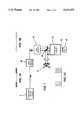
- FIG. 1is a drawing showing the principal features of a preferred embodiment of the present invention for producing high brightness pulse laser beams useful for X-ray lithography.
- FIGS. 1A, 1B and 1Care qualitative representations of the pulse shape at various stages of the embodiment shown in FIG. 1.
- FIG. 2is a drawing showing in greater detain a first portion of the embodiment of FIG. 1.
- FIG. 3is a drawing showing in greater detail a second portion of the embodiment shown in FIG. 1.
- FIG. 4is a drawing showing the amplifier pumping configuration using laser diodes for the embodiment shown in FIG. 1.
- FIG. 5is a drawing showing a cluster of tightly focused spots.
- FIGS. 1, 2 and 3A preferred embodiment of the present invention can be described by reference to FIGS. 1, 2 and 3.
- this embodimentconsists of a mode locked Nd:YAG laser oscillator 2, a pulse spacing selector 20, a beam expander 22, a polarizing beam splitter 26, a double pass amplifier section 24 and a beam steering PZT 48 on which the amplifier folding mirror 38 is mounted.
- the output of amplifier 24is focused to a tiny spot on moving copper tape target 27.
- FIG. 2describes the seed laser laser section of the embodiment which is for producing very short duration pulses at a very high repetition rate and FIG.
- FIG. 3describes the amplifying section for amplifying the pulses to produce a pulsed laser beam with an average power level of about 1 kW with pulses at brightness levels in the range of 10 14 W/cm 2 on spot sizes of about 20 ⁇ m diameter.
- FIG. 5shows the result of a beam steering mechanism to generate a cluster of few 20 ⁇ m spots 52 over a 500 ⁇ m diameter circular area on a metal target.
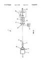
- FIG. 2is a diagram of a Nd:YAG mode locked oscillator type laser device 2.
- a Nd:YAG polished rod 4(3 mm diameter and 2.5 cm long) is longitudinally pumped by a 5 bar impingement cooled laser diode array 6 (part number SDL3245-J5).
- the diode pump arrayis a quasi-CW at 20 percent duty factor (about 200 ⁇ s ON and 800 ⁇ s OFF) and 50 Watt average.
- the diode array wavelengthis at 808 nm which corresponds to strong absorption in the Nd:YAG.
- the output of the pump diodesare collimated in the longitudinal axis by an array of cylindrical micro-lenses 8.
- a fast focusing lens 10concentrates the pump light at the back end of Nd:YAG crystal 4.
- the back surface of Nd:YAG crystal 4has 5 m radius of curvature (convex) and is polished and coated for maximum reflection (about 99.8 percent) at 1064 nm (the lasing wavelength of the Nd:YAG laser) and for at least 85 percent transmission for 808 nm (the pump wavelength).
- the pump lightis trapped in the laser rod via total internal reflection (similar to a fiber optics) for high pumping efficiency.
- the front surface 12 of the Nd:YAG rodis cut at 2 degrees to avoid parasitic oscillations and AR coated for minimal insertion loses at 1064 nm.
- a Brewster cut acousto-optic mode locker 14(Brimrose Corporation of America Model FSML-38-10-BR-1064) is placed next to a partially transmitting mirror 16 (output coupler) to actively force all the longitudinal modes to be in phase each time they pass the mode locker.
- the RF carrier frequency (f) of the mode locker and the optical length of the laser resonator (L)must relate as follows:
- cis the speed of light.
- a train of mode locked pulses at 76 MHz (due to the standing waves that form in the acousto-optic cell) during the ON timewill be obtained.
- the pulse durationwill be about 100 ps with an energy per pulse of about 0.6 ⁇ J.
- the time interval between pulses during the 200 ⁇ s diode ON periodsis about 13 ns. During each ON period we get about 15,200 of these very short pulses. Then we have a dead time of about 800 ⁇ s before the next series of 15,200 short pulses.
- FIG. 1AA qualitative depiction of this pulse train is shown in FIG. 1A.
- the rapid series of pulsesrepresent 15,200 pulses each with an energy of about 0.6 ⁇ J per pulse spread over 200 ⁇ s and the space represents an 800 ⁇ s dead time.
- Pulse spacing selector 20consists in this embodiment of an electro-optic modulator such as Model 305 supplied by ConOptics. This unit will function as a fast shutter to pass light from the beam during short intervals (each interval having a duration of about 10 ns) at a frequency of 60,000 Hz.
- the pulse selector(synchronized with the beam) will pass a single pulse through each 10 ns window and block all other pulses. At our frequency of 60,000 Hz, we will therefore have about 12 pulses pass each 200 ⁇ s ON period. Since we have 1,000 of these ON periods each second, we will get about 12,000 pulses per second.
- the output of pulse spacing selector 20is a pulse train consisting of clumps of about 12 pulses (each pulse having a duration of about 100 ⁇ s) spaced over 200 ⁇ s duration and these clumps of short pulses being spaced at intervals of 1,000 per second. This is an average of 12,000 pulses per second. To summarize, the output of pulse spacing selector is as follows:
- FIG. 1BA qualitative depiction of this pulse train is shown graphically in FIG. 1B. It is essentially the same as the train shown in FIG. 1A except the frequency of the pulses during the ON period has been reduced by a factor of about 1,260.
- the output of the pulse spacing selectoris expanded from a cross section of about 0.07 cm 2 to a cross section of about 0.6 cm 2 with a 3:1 beam expander 22 as shown in FIG. 2.
- Beam expander 22consist of an appropriate combination of lenses or any of several commercially available beam expanders chosen for the 1064 nm Nd:YAG beam.
- the output of beam expander 22is directed to amplifier 24 as shown in FIG. 1.
- Amplifier 24 for this preferred embodimentis shown if FIG. 1 and in greater detail in FIGS. 3 and 4.
- FIG. 3shows the principal features of amplifier other than the amplifier pumping equipment.
- the linearly polarized beam 21 from beam expanderpasses through a thin film polarizing beam splitter 26 and into a first Nd:YAG amplifier rod 28 then through a one half wavelength rotator 30 (to cancel thermally induced bi-refringence) then through a second Nd:YAG amplifier rod 32 then through quarter wave plate 34 (for shifting the polarization of the outgoing beam by 90 degrees) and corrector lens 36 (for correcting the thermal lensing in the Nd rods) and is reflected off high reflectivity (HR) mirror 38.
- HRhigh reflectivity
- the beampasses back through the elements of amplifier 24 for two pass amplification and reflected off polarizing beam splitter 26 from which the beam is focused and directed to a metal target 27 as shown in FIG. 1.
- the amplifier pumping equipmentis shown in FIG. 4.
- This equipmentincludes 64 modules of 50 Watt per module (nominal) laser diode arrays 40 for a total of about 3 KW average power operating at 808 nm wavelength, 20 percent duty factor (200 ⁇ s ON and 800 ⁇ s OFF).
- 16 setsare arranged as shown in FIG. 4.
- the output of the diode lasersare directed into the Nd:YAG rods 28 and 32 with cylindrical lenses 42 and the rods are water cooled by water jacket 44 as shown in FIG. 4.
- Amplifier 24provides a 1.3 ⁇ 10 5 amplification of the input beam with good preservation of the input beam (near diffraction limited beam, less than or equal to 2 ⁇ DL). We focus the beam to a 20 ⁇ m spot on the target.
- the output of Amplifier 24is a pulsed laser beam with the following characteristics:
- FIG. 1CA qualitative description of the output of the amplifier is shown in FIG. 1C. It is substantially the same as the pulse train shown in FIG. 1B except the pulses are amplified in energy by a factor of about 133,000.
- Preferred sizes of the X-ray point source for proximity lithographyis in the range of a few 100 ⁇ m (e.g., 500 ⁇ m) in diameter to about 1 mm in diameter.
- a 500 ⁇ m spot simulated from 20 ⁇ m diameter pulsesis shown in FIG. 5.
- we have to hit the target at different spotse.g., multiple 20 ⁇ m spots 52 spread over a 500 ⁇ m area 50. This can be accomplished by a mirror mounted on a fast 2 axis PZT 48 that would steer the beam slightly over the required area as shown in FIG. 1.
- the above systemprovides very good X-ray conversion. However, a somewhat better X-ray conversion can be accomplished with higher frequency beams. In a study by Lawrence Livermore laboratories, a 15 percent conversion efficiency was observed when the laser wavelength was 532 nm (doubled 1064 nm) versus 10 percent conversion efficiency for 1064 nm. A doubling crystal can be placed at the output beam from the amplifier in order to utilize the higher X-ray conversion efficiency at 532 nm.
- the cost of laser diodes for pumping solid state lasersis primarily dominated by the peak power requirements and this determines the number of diode bars.
- a 1 KW systemmay require 3 KW average power from the pump diodes
- a 20 percent duty factor diode array systemwould require 15 KW peak power.
- 50 Watt peak bars at $700 per barthe system would cost $210,000.
- a 1 percent duty factor systemwould require 300 KW peak power.
- the costwould be $4,000,000.
- Increasing the duty factor above 20 percent, all the way to CWis feasible, but, balancing all factors we prefer a duty factor of about 20 percent.
- a flash lamp pumping systemcould replace the diode pumping system.
- the seed beam pulse train frequencycould be in the range of 10 MHz to 200 MHz or greater. With some compromise in the average power the number of pulses per second could be reduces down to about 1,000 Hz.
- High repetition rate mode locked Q-switched systemscan be used to generate pulses that are composed of multiple pulses for prepulse applications.
- the amplifiercan be of slab or rod design.
- the solid state materialcan be of a host material other than Nd:YAG. For example, Nd:YLF, Cr:LiSAF, Ti:S, etc. could be used.
- the steering mirrorcan be any reflecting element that would be appropriate to generate the cluster of spot sizes desired, such as the 20 ⁇ m spots.
- pulse spacing devicescould be substituted for the electro-optic modulator for pulse spacing, such as cavity dumping or even an optical rotary interrupter.
- the pulse spacing deviceswould in most applications remove a very large percentage of the pulses in the seed beam such as more than 99 percent as in the preferred embodiment described; however, We could imagine applications where as the percentage remove might be as low as 80 percent.
- the number of passes through the amplifiercan be as high as eight. Systems with eight passes are clearly feasible.
Landscapes
- Physics & Mathematics (AREA)
- Electromagnetism (AREA)
- Engineering & Computer Science (AREA)
- Optics & Photonics (AREA)
- Plasma & Fusion (AREA)
- Lasers (AREA)
Abstract
Description
f=c/4L
______________________________________ Pulse duration about 100 ps Energy per pulse 0.6 μJ Peak power perpulse 6 kW Average frequency 12,000 pulses per second Average power 7.2 mW Beam cross section 0.07 cm.sup.2 ______________________________________
______________________________________ Pulse duration about 100 ps Energy per pulse 80 mJ/pulse Peak power per pulse 800 MW Average frequency 12,000 pulses per second Average power 1 kW Beam diameter 9 mm Brightness (power/ 2.5 × 10.sup.14 Watts/cm.sup.2 (20 μm dia. spot) pulse) ______________________________________
Claims (22)
Priority Applications (6)
| Application Number | Priority Date | Filing Date | Title |
|---|---|---|---|
| US08/295,283US5434875A (en) | 1994-08-24 | 1994-08-24 | Low cost, high average power, high brightness solid state laser |
| US08/339,755US5491707A (en) | 1994-08-24 | 1994-11-15 | Low cost, high average power, high brightness solid state laser |
| US08/434,860US5539764A (en) | 1994-08-24 | 1995-05-04 | Laser generated X-ray source |
| US08/725,750US5742634A (en) | 1994-08-24 | 1996-10-04 | Picosecond laser |
| US08/845,185US5790574A (en) | 1994-08-24 | 1997-04-21 | Low cost, high average power, high brightness solid state laser |
| US09/058,274US6016324A (en) | 1994-08-24 | 1998-04-09 | Short pulse laser system |
Applications Claiming Priority (1)
| Application Number | Priority Date | Filing Date | Title |
|---|---|---|---|
| US08/295,283US5434875A (en) | 1994-08-24 | 1994-08-24 | Low cost, high average power, high brightness solid state laser |
Related Child Applications (3)
| Application Number | Title | Priority Date | Filing Date |
|---|---|---|---|
| US08/339,755Continuation-In-PartUS5491707A (en) | 1994-08-24 | 1994-11-15 | Low cost, high average power, high brightness solid state laser |
| US08/434,860Continuation-In-PartUS5539764A (en) | 1994-08-24 | 1995-05-04 | Laser generated X-ray source |
| US50337395AContinuation-In-Part | 1994-08-24 | 1995-07-17 |
Publications (1)
| Publication Number | Publication Date |
|---|---|
| US5434875Atrue US5434875A (en) | 1995-07-18 |
Family
ID=23137043
Family Applications (1)
| Application Number | Title | Priority Date | Filing Date |
|---|---|---|---|
| US08/295,283Expired - Fee RelatedUS5434875A (en) | 1994-08-24 | 1994-08-24 | Low cost, high average power, high brightness solid state laser |
Country Status (1)
| Country | Link |
|---|---|
| US (1) | US5434875A (en) |
Cited By (63)
| Publication number | Priority date | Publication date | Assignee | Title |
|---|---|---|---|---|
| US5790574A (en)* | 1994-08-24 | 1998-08-04 | Imar Technology Company | Low cost, high average power, high brightness solid state laser |
| WO1998026328A3 (en)* | 1996-11-29 | 1998-10-29 | Laser Optics Res Corp | Monochromatic r,g,b laser light source display system and method |
| US5963575A (en)* | 1993-03-27 | 1999-10-05 | Clyxon Laser Fur Mediziner GmbH | Q-switched laser system, in particular for laser lithotripsy |
| EP0792530A4 (en)* | 1994-11-15 | 2000-01-19 | Jmar Technology Co | HIGH BRIGHTNESS, HIGH MEDIUM POWER AND LOW COST SOLID LASER |
| US6272156B1 (en)* | 1998-01-28 | 2001-08-07 | Coherent, Inc. | Apparatus for ultrashort pulse transportation and delivery |
| EP1107403A3 (en)* | 1999-12-03 | 2001-09-26 | Mitsubishi Denki Kabushiki Kaisha | Solid-state laser oscillator |
| US6310715B1 (en)* | 2000-04-26 | 2001-10-30 | The United States Of America As Represented By The United States Air Force | Crystal stack for coherent optical beam combination |
| US6335942B1 (en)* | 1999-10-08 | 2002-01-01 | National Science Council Of Republic Of China | Frequency stabilized passively Q-switched laser |
| US6389101B1 (en) | 1999-05-24 | 2002-05-14 | Jmar Research, Inc. | Parallel x-ray nanotomography |
| US20040052278A1 (en)* | 2001-08-10 | 2004-03-18 | Lightwave Electronics Corporation | Fiber amplifier system for producing visible light |
| US6717719B1 (en)* | 2001-10-01 | 2004-04-06 | The United States Of America As Represented By The Secretary Of The Air Force | Coherent optical beam combination using double-coated glass mirrors/mirror pairs |
| US6744803B2 (en) | 2002-01-17 | 2004-06-01 | Northrop Grumman Corporation | High brightness laser oscillator with spherical aberration |
| US20050180043A1 (en)* | 2003-12-17 | 2005-08-18 | Jmar Research Inc. | Systems and methods for tape advancement in laser produced plasma equipment |
| US20060067476A1 (en)* | 2004-07-27 | 2006-03-30 | Jmar Research, Inc. | Rotating shutter for laser-produced plasma debris mitigation |
| US20060159138A1 (en)* | 2004-12-21 | 2006-07-20 | Institut National D'optique | Pulsed laser light source |
| US7116687B2 (en) | 2003-09-12 | 2006-10-03 | Jds Uniphase Corporation | High repetition rate passively Q-switched laser for blue laser based on interactions in fiber |
| US20060262815A1 (en)* | 2005-05-23 | 2006-11-23 | Time-Bandwidth Products Ag | Light pulse generating apparatus and method |
| US20070195322A1 (en)* | 2005-10-11 | 2007-08-23 | Jmar Research, Inc. | Multipulse agile laser source for real time spark spectrochemical hazard analysis |
| US20070258493A1 (en)* | 2006-05-02 | 2007-11-08 | Northrop Grumman Corporation | Laser power reduction without mode change |
| US20080069157A1 (en)* | 2006-08-29 | 2008-03-20 | Tatsuya Ariga | Driver laser for extreme ultra violet light source device |
| US20080240347A1 (en)* | 2005-07-22 | 2008-10-02 | Jmar Research, Inc. | Method, apparatus, and system for extending depth of field (dof) in a short-wavelength microscope using wavefront encoding |
| US7489437B1 (en) | 2007-12-05 | 2009-02-10 | Corning Incorporated | Fiber laser red-green-blue (RGB) light source |
| US7586958B2 (en) | 2006-09-29 | 2009-09-08 | Northrop Grumman Corporation | Electro-opto switching of unpolarized lasers |
| US20100078580A1 (en)* | 2008-09-26 | 2010-04-01 | Gigaphoton Inc. | Extreme ultraviolet light source device, laser light source device for extreme ultraviolet light source device and method for controlling saturable absorber used in extreme ultraviolet light source device |
| CN102122118A (en)* | 2011-02-23 | 2011-07-13 | 中国科学院上海光学精密机械研究所 | Laser direct writing device |
| FR2999023A1 (en)* | 2012-12-04 | 2014-06-06 | Amplitude Systemes | SYSTEM AND METHOD FOR GENERATING HIGH-POWER ULTRACOURSE LASER PULSE SALVATION |
| US9676167B2 (en) | 2013-12-17 | 2017-06-13 | Corning Incorporated | Laser processing of sapphire substrate and related applications |
| US20170189991A1 (en)* | 2014-07-14 | 2017-07-06 | Corning Incorporated | Systems and methods for processing transparent materials using adjustable laser beam focal lines |
| US9701563B2 (en) | 2013-12-17 | 2017-07-11 | Corning Incorporated | Laser cut composite glass article and method of cutting |
| US9815144B2 (en) | 2014-07-08 | 2017-11-14 | Corning Incorporated | Methods and apparatuses for laser processing materials |
| US9815730B2 (en) | 2013-12-17 | 2017-11-14 | Corning Incorporated | Processing 3D shaped transparent brittle substrate |
| US9850159B2 (en) | 2012-11-20 | 2017-12-26 | Corning Incorporated | High speed laser processing of transparent materials |
| US9850160B2 (en) | 2013-12-17 | 2017-12-26 | Corning Incorporated | Laser cutting of display glass compositions |
| US10047001B2 (en) | 2014-12-04 | 2018-08-14 | Corning Incorporated | Glass cutting systems and methods using non-diffracting laser beams |
| US10144093B2 (en) | 2013-12-17 | 2018-12-04 | Corning Incorporated | Method for rapid laser drilling of holes in glass and products made therefrom |
| US10173916B2 (en) | 2013-12-17 | 2019-01-08 | Corning Incorporated | Edge chamfering by mechanically processing laser cut glass |
| US10233112B2 (en) | 2013-12-17 | 2019-03-19 | Corning Incorporated | Laser processing of slots and holes |
| US10252931B2 (en) | 2015-01-12 | 2019-04-09 | Corning Incorporated | Laser cutting of thermally tempered substrates |
| US10280108B2 (en) | 2013-03-21 | 2019-05-07 | Corning Laser Technologies GmbH | Device and method for cutting out contours from planar substrates by means of laser |
| US10335902B2 (en) | 2014-07-14 | 2019-07-02 | Corning Incorporated | Method and system for arresting crack propagation |
| US10377658B2 (en) | 2016-07-29 | 2019-08-13 | Corning Incorporated | Apparatuses and methods for laser processing |
| US10421683B2 (en) | 2013-01-15 | 2019-09-24 | Corning Laser Technologies GmbH | Method and device for the laser-based machining of sheet-like substrates |
| US10522963B2 (en) | 2016-08-30 | 2019-12-31 | Corning Incorporated | Laser cutting of materials with intensity mapping optical system |
| US10526234B2 (en) | 2014-07-14 | 2020-01-07 | Corning Incorporated | Interface block; system for and method of cutting a substrate being transparent within a range of wavelengths using such interface block |
| US10525657B2 (en) | 2015-03-27 | 2020-01-07 | Corning Incorporated | Gas permeable window and method of fabricating the same |
| US10611667B2 (en) | 2014-07-14 | 2020-04-07 | Corning Incorporated | Method and system for forming perforations |
| US10626040B2 (en) | 2017-06-15 | 2020-04-21 | Corning Incorporated | Articles capable of individual singulation |
| US10688599B2 (en) | 2017-02-09 | 2020-06-23 | Corning Incorporated | Apparatus and methods for laser processing transparent workpieces using phase shifted focal lines |
| US10730783B2 (en) | 2016-09-30 | 2020-08-04 | Corning Incorporated | Apparatuses and methods for laser processing transparent workpieces using non-axisymmetric beam spots |
| US10752534B2 (en) | 2016-11-01 | 2020-08-25 | Corning Incorporated | Apparatuses and methods for laser processing laminate workpiece stacks |
| US11062986B2 (en) | 2017-05-25 | 2021-07-13 | Corning Incorporated | Articles having vias with geometry attributes and methods for fabricating the same |
| US11078112B2 (en) | 2017-05-25 | 2021-08-03 | Corning Incorporated | Silica-containing substrates with vias having an axially variable sidewall taper and methods for forming the same |
| US11111170B2 (en) | 2016-05-06 | 2021-09-07 | Corning Incorporated | Laser cutting and removal of contoured shapes from transparent substrates |
| US11114309B2 (en) | 2016-06-01 | 2021-09-07 | Corning Incorporated | Articles and methods of forming vias in substrates |
| US11121521B2 (en)* | 2019-02-25 | 2021-09-14 | Kla Corporation | System and method for pumping laser sustained plasma with interlaced pulsed illumination sources |
| US11186060B2 (en) | 2015-07-10 | 2021-11-30 | Corning Incorporated | Methods of continuous fabrication of holes in flexible substrate sheets and products relating to the same |
| US20220339741A1 (en)* | 2019-09-06 | 2022-10-27 | Ire-Polus | Method of laser beam machining of a transparent brittle material and device embodying such method |
| US11542190B2 (en) | 2016-10-24 | 2023-01-03 | Corning Incorporated | Substrate processing station for laser-based machining of sheet-like glass substrates |
| US11556039B2 (en) | 2013-12-17 | 2023-01-17 | Corning Incorporated | Electrochromic coated glass articles and methods for laser processing the same |
| US11554984B2 (en) | 2018-02-22 | 2023-01-17 | Corning Incorporated | Alkali-free borosilicate glasses with low post-HF etch roughness |
| US11773004B2 (en) | 2015-03-24 | 2023-10-03 | Corning Incorporated | Laser cutting and processing of display glass compositions |
| US11774233B2 (en) | 2016-06-29 | 2023-10-03 | Corning Incorporated | Method and system for measuring geometric parameters of through holes |
| US12180108B2 (en) | 2017-12-19 | 2024-12-31 | Corning Incorporated | Methods for etching vias in glass-based articles employing positive charge organic molecules |
Citations (2)
| Publication number | Priority date | Publication date | Assignee | Title |
|---|---|---|---|---|
| US5003543A (en)* | 1990-01-19 | 1991-03-26 | California Jamar, Incorporated | Laser plasma X-ray source |
| US5235606A (en)* | 1991-10-29 | 1993-08-10 | University Of Michigan | Amplification of ultrashort pulses with nd:glass amplifiers pumped by alexandrite free running laser |
- 1994
- 1994-08-24USUS08/295,283patent/US5434875A/ennot_activeExpired - Fee Related
Patent Citations (2)
| Publication number | Priority date | Publication date | Assignee | Title |
|---|---|---|---|---|
| US5003543A (en)* | 1990-01-19 | 1991-03-26 | California Jamar, Incorporated | Laser plasma X-ray source |
| US5235606A (en)* | 1991-10-29 | 1993-08-10 | University Of Michigan | Amplification of ultrashort pulses with nd:glass amplifiers pumped by alexandrite free running laser |
Non-Patent Citations (2)
| Title |
|---|
| Xenakis et al., Laser plasma x ray generator using an injection mode locked XeCl excimer Laser, 1 Jan. 1992.* |
| Xenakis et al., Laser-plasma x-ray generator using an injection-mode-locked-XeCl excimer Laser, 1 Jan. 1992. |
Cited By (94)
| Publication number | Priority date | Publication date | Assignee | Title |
|---|---|---|---|---|
| US5963575A (en)* | 1993-03-27 | 1999-10-05 | Clyxon Laser Fur Mediziner GmbH | Q-switched laser system, in particular for laser lithotripsy |
| US5790574A (en)* | 1994-08-24 | 1998-08-04 | Imar Technology Company | Low cost, high average power, high brightness solid state laser |
| EP0792530A4 (en)* | 1994-11-15 | 2000-01-19 | Jmar Technology Co | HIGH BRIGHTNESS, HIGH MEDIUM POWER AND LOW COST SOLID LASER |
| US6774881B2 (en) | 1996-11-29 | 2004-08-10 | Corporation For Laser Optics Research | Monochromatic R,G,B laser display system and method |
| WO1998026328A3 (en)* | 1996-11-29 | 1998-10-29 | Laser Optics Res Corp | Monochromatic r,g,b laser light source display system and method |
| AU723680B2 (en)* | 1996-11-29 | 2000-08-31 | Christie Digital Systems Usa, Inc. | Monochromatic R,G,B laser light source display system and method |
| US6304237B1 (en) | 1996-11-29 | 2001-10-16 | Corporation For Laser Optics Research | Monochromatic R,G,B laser light source display system and method |
| US6272156B1 (en)* | 1998-01-28 | 2001-08-07 | Coherent, Inc. | Apparatus for ultrashort pulse transportation and delivery |
| US6389101B1 (en) | 1999-05-24 | 2002-05-14 | Jmar Research, Inc. | Parallel x-ray nanotomography |
| US6335942B1 (en)* | 1999-10-08 | 2002-01-01 | National Science Council Of Republic Of China | Frequency stabilized passively Q-switched laser |
| EP1107403A3 (en)* | 1999-12-03 | 2001-09-26 | Mitsubishi Denki Kabushiki Kaisha | Solid-state laser oscillator |
| US6310715B1 (en)* | 2000-04-26 | 2001-10-30 | The United States Of America As Represented By The United States Air Force | Crystal stack for coherent optical beam combination |
| US20040052278A1 (en)* | 2001-08-10 | 2004-03-18 | Lightwave Electronics Corporation | Fiber amplifier system for producing visible light |
| US7039076B2 (en) | 2001-08-10 | 2006-05-02 | Jds Uniphase Corporation | Fiber amplifier system for producing visible light |
| US6717719B1 (en)* | 2001-10-01 | 2004-04-06 | The United States Of America As Represented By The Secretary Of The Air Force | Coherent optical beam combination using double-coated glass mirrors/mirror pairs |
| US6744803B2 (en) | 2002-01-17 | 2004-06-01 | Northrop Grumman Corporation | High brightness laser oscillator with spherical aberration |
| US7116687B2 (en) | 2003-09-12 | 2006-10-03 | Jds Uniphase Corporation | High repetition rate passively Q-switched laser for blue laser based on interactions in fiber |
| US20050180043A1 (en)* | 2003-12-17 | 2005-08-18 | Jmar Research Inc. | Systems and methods for tape advancement in laser produced plasma equipment |
| US7424096B2 (en) | 2003-12-17 | 2008-09-09 | Jmar Research, Inc. | Systems and methods for tape advancement in laser produced plasma equipment |
| US20060067476A1 (en)* | 2004-07-27 | 2006-03-30 | Jmar Research, Inc. | Rotating shutter for laser-produced plasma debris mitigation |
| US7302043B2 (en) | 2004-07-27 | 2007-11-27 | Gatan, Inc. | Rotating shutter for laser-produced plasma debris mitigation |
| US20060159138A1 (en)* | 2004-12-21 | 2006-07-20 | Institut National D'optique | Pulsed laser light source |
| US20060262815A1 (en)* | 2005-05-23 | 2006-11-23 | Time-Bandwidth Products Ag | Light pulse generating apparatus and method |
| US7386019B2 (en)* | 2005-05-23 | 2008-06-10 | Time-Bandwidth Products Ag | Light pulse generating apparatus and method |
| US20080240347A1 (en)* | 2005-07-22 | 2008-10-02 | Jmar Research, Inc. | Method, apparatus, and system for extending depth of field (dof) in a short-wavelength microscope using wavefront encoding |
| US20070195322A1 (en)* | 2005-10-11 | 2007-08-23 | Jmar Research, Inc. | Multipulse agile laser source for real time spark spectrochemical hazard analysis |
| US7688443B2 (en) | 2005-10-11 | 2010-03-30 | Jmar Llc | Multipulse agile laser source for real time spark spectrochemical hazard analysis |
| US20070258493A1 (en)* | 2006-05-02 | 2007-11-08 | Northrop Grumman Corporation | Laser power reduction without mode change |
| US7460566B2 (en) | 2006-05-02 | 2008-12-02 | Northrop Grumman Corporation | Laser power reduction without mode change |
| US20110211601A1 (en)* | 2006-08-29 | 2011-09-01 | Tatsuya Ariga | Driver laser for extreme ultra violet light source device |
| US20080069157A1 (en)* | 2006-08-29 | 2008-03-20 | Tatsuya Ariga | Driver laser for extreme ultra violet light source device |
| US7586958B2 (en) | 2006-09-29 | 2009-09-08 | Northrop Grumman Corporation | Electro-opto switching of unpolarized lasers |
| US7489437B1 (en) | 2007-12-05 | 2009-02-10 | Corning Incorporated | Fiber laser red-green-blue (RGB) light source |
| US8476609B2 (en) | 2008-09-26 | 2013-07-02 | Gigaphoton Inc. | Extreme ultraviolet light source device, laser light source device for extreme ultraviolet light source device, and method for controlling saturable absorber used in extreme ultraviolet light source device |
| US8093571B2 (en) | 2008-09-26 | 2012-01-10 | Gigaphoton Inc. | Extreme ultraviolet light source device, laser light source device for extreme ultraviolet light source device and method for controlling saturable absorber used in extreme ultraviolet light source device |
| US20100078580A1 (en)* | 2008-09-26 | 2010-04-01 | Gigaphoton Inc. | Extreme ultraviolet light source device, laser light source device for extreme ultraviolet light source device and method for controlling saturable absorber used in extreme ultraviolet light source device |
| CN102122118A (en)* | 2011-02-23 | 2011-07-13 | 中国科学院上海光学精密机械研究所 | Laser direct writing device |
| US9850159B2 (en) | 2012-11-20 | 2017-12-26 | Corning Incorporated | High speed laser processing of transparent materials |
| FR2999023A1 (en)* | 2012-12-04 | 2014-06-06 | Amplitude Systemes | SYSTEM AND METHOD FOR GENERATING HIGH-POWER ULTRACOURSE LASER PULSE SALVATION |
| WO2014087104A3 (en)* | 2012-12-04 | 2014-08-14 | Amplitude Systemes | System and method for generating a burst of ultra-short, high-power laser pulses |
| US9525264B2 (en) | 2012-12-04 | 2016-12-20 | Amplitude Systemes | System and method for generating a burst of ultra-short, high-power laser pulses |
| US11345625B2 (en) | 2013-01-15 | 2022-05-31 | Corning Laser Technologies GmbH | Method and device for the laser-based machining of sheet-like substrates |
| US11028003B2 (en) | 2013-01-15 | 2021-06-08 | Corning Laser Technologies GmbH | Method and device for laser-based machining of flat substrates |
| US10421683B2 (en) | 2013-01-15 | 2019-09-24 | Corning Laser Technologies GmbH | Method and device for the laser-based machining of sheet-like substrates |
| US11713271B2 (en) | 2013-03-21 | 2023-08-01 | Corning Laser Technologies GmbH | Device and method for cutting out contours from planar substrates by means of laser |
| US10280108B2 (en) | 2013-03-21 | 2019-05-07 | Corning Laser Technologies GmbH | Device and method for cutting out contours from planar substrates by means of laser |
| US9850160B2 (en) | 2013-12-17 | 2017-12-26 | Corning Incorporated | Laser cutting of display glass compositions |
| US11148225B2 (en) | 2013-12-17 | 2021-10-19 | Corning Incorporated | Method for rapid laser drilling of holes in glass and products made therefrom |
| US10144093B2 (en) | 2013-12-17 | 2018-12-04 | Corning Incorporated | Method for rapid laser drilling of holes in glass and products made therefrom |
| US10173916B2 (en) | 2013-12-17 | 2019-01-08 | Corning Incorporated | Edge chamfering by mechanically processing laser cut glass |
| US10179748B2 (en) | 2013-12-17 | 2019-01-15 | Corning Incorporated | Laser processing of sapphire substrate and related applications |
| US10183885B2 (en) | 2013-12-17 | 2019-01-22 | Corning Incorporated | Laser cut composite glass article and method of cutting |
| US10233112B2 (en) | 2013-12-17 | 2019-03-19 | Corning Incorporated | Laser processing of slots and holes |
| US9676167B2 (en) | 2013-12-17 | 2017-06-13 | Corning Incorporated | Laser processing of sapphire substrate and related applications |
| US9815730B2 (en) | 2013-12-17 | 2017-11-14 | Corning Incorporated | Processing 3D shaped transparent brittle substrate |
| US10293436B2 (en) | 2013-12-17 | 2019-05-21 | Corning Incorporated | Method for rapid laser drilling of holes in glass and products made therefrom |
| US11556039B2 (en) | 2013-12-17 | 2023-01-17 | Corning Incorporated | Electrochromic coated glass articles and methods for laser processing the same |
| US9701563B2 (en) | 2013-12-17 | 2017-07-11 | Corning Incorporated | Laser cut composite glass article and method of cutting |
| US10392290B2 (en) | 2013-12-17 | 2019-08-27 | Corning Incorporated | Processing 3D shaped transparent brittle substrate |
| US10611668B2 (en) | 2013-12-17 | 2020-04-07 | Corning Incorporated | Laser cut composite glass article and method of cutting |
| US10442719B2 (en) | 2013-12-17 | 2019-10-15 | Corning Incorporated | Edge chamfering methods |
| US10597321B2 (en) | 2013-12-17 | 2020-03-24 | Corning Incorporated | Edge chamfering methods |
| US11697178B2 (en) | 2014-07-08 | 2023-07-11 | Corning Incorporated | Methods and apparatuses for laser processing materials |
| US9815144B2 (en) | 2014-07-08 | 2017-11-14 | Corning Incorporated | Methods and apparatuses for laser processing materials |
| US10526234B2 (en) | 2014-07-14 | 2020-01-07 | Corning Incorporated | Interface block; system for and method of cutting a substrate being transparent within a range of wavelengths using such interface block |
| US20170189991A1 (en)* | 2014-07-14 | 2017-07-06 | Corning Incorporated | Systems and methods for processing transparent materials using adjustable laser beam focal lines |
| US10611667B2 (en) | 2014-07-14 | 2020-04-07 | Corning Incorporated | Method and system for forming perforations |
| US10335902B2 (en) | 2014-07-14 | 2019-07-02 | Corning Incorporated | Method and system for arresting crack propagation |
| US11648623B2 (en)* | 2014-07-14 | 2023-05-16 | Corning Incorporated | Systems and methods for processing transparent materials using adjustable laser beam focal lines |
| US11014845B2 (en) | 2014-12-04 | 2021-05-25 | Corning Incorporated | Method of laser cutting glass using non-diffracting laser beams |
| US10047001B2 (en) | 2014-12-04 | 2018-08-14 | Corning Incorporated | Glass cutting systems and methods using non-diffracting laser beams |
| US10252931B2 (en) | 2015-01-12 | 2019-04-09 | Corning Incorporated | Laser cutting of thermally tempered substrates |
| US11773004B2 (en) | 2015-03-24 | 2023-10-03 | Corning Incorporated | Laser cutting and processing of display glass compositions |
| US10525657B2 (en) | 2015-03-27 | 2020-01-07 | Corning Incorporated | Gas permeable window and method of fabricating the same |
| US11186060B2 (en) | 2015-07-10 | 2021-11-30 | Corning Incorporated | Methods of continuous fabrication of holes in flexible substrate sheets and products relating to the same |
| US11111170B2 (en) | 2016-05-06 | 2021-09-07 | Corning Incorporated | Laser cutting and removal of contoured shapes from transparent substrates |
| US11114309B2 (en) | 2016-06-01 | 2021-09-07 | Corning Incorporated | Articles and methods of forming vias in substrates |
| US11774233B2 (en) | 2016-06-29 | 2023-10-03 | Corning Incorporated | Method and system for measuring geometric parameters of through holes |
| US10377658B2 (en) | 2016-07-29 | 2019-08-13 | Corning Incorporated | Apparatuses and methods for laser processing |
| US10522963B2 (en) | 2016-08-30 | 2019-12-31 | Corning Incorporated | Laser cutting of materials with intensity mapping optical system |
| US11130701B2 (en) | 2016-09-30 | 2021-09-28 | Corning Incorporated | Apparatuses and methods for laser processing transparent workpieces using non-axisymmetric beam spots |
| US10730783B2 (en) | 2016-09-30 | 2020-08-04 | Corning Incorporated | Apparatuses and methods for laser processing transparent workpieces using non-axisymmetric beam spots |
| US11542190B2 (en) | 2016-10-24 | 2023-01-03 | Corning Incorporated | Substrate processing station for laser-based machining of sheet-like glass substrates |
| US10752534B2 (en) | 2016-11-01 | 2020-08-25 | Corning Incorporated | Apparatuses and methods for laser processing laminate workpiece stacks |
| US10688599B2 (en) | 2017-02-09 | 2020-06-23 | Corning Incorporated | Apparatus and methods for laser processing transparent workpieces using phase shifted focal lines |
| US11078112B2 (en) | 2017-05-25 | 2021-08-03 | Corning Incorporated | Silica-containing substrates with vias having an axially variable sidewall taper and methods for forming the same |
| US11062986B2 (en) | 2017-05-25 | 2021-07-13 | Corning Incorporated | Articles having vias with geometry attributes and methods for fabricating the same |
| US11972993B2 (en) | 2017-05-25 | 2024-04-30 | Corning Incorporated | Silica-containing substrates with vias having an axially variable sidewall taper and methods for forming the same |
| US10626040B2 (en) | 2017-06-15 | 2020-04-21 | Corning Incorporated | Articles capable of individual singulation |
| US12180108B2 (en) | 2017-12-19 | 2024-12-31 | Corning Incorporated | Methods for etching vias in glass-based articles employing positive charge organic molecules |
| US11554984B2 (en) | 2018-02-22 | 2023-01-17 | Corning Incorporated | Alkali-free borosilicate glasses with low post-HF etch roughness |
| KR20210121283A (en)* | 2019-02-25 | 2021-10-07 | 케이엘에이 코포레이션 | System and method for pumping laser sustained plasma with interlaced pulsed illumination sources |
| US11121521B2 (en)* | 2019-02-25 | 2021-09-14 | Kla Corporation | System and method for pumping laser sustained plasma with interlaced pulsed illumination sources |
| US20220339741A1 (en)* | 2019-09-06 | 2022-10-27 | Ire-Polus | Method of laser beam machining of a transparent brittle material and device embodying such method |
Similar Documents
| Publication | Publication Date | Title |
|---|---|---|
| US5434875A (en) | Low cost, high average power, high brightness solid state laser | |
| US5491707A (en) | Low cost, high average power, high brightness solid state laser | |
| US5790574A (en) | Low cost, high average power, high brightness solid state laser | |
| US5689363A (en) | Long-pulse-width narrow-bandwidth solid state laser | |
| KR100339057B1 (en) | Short pulse laser system | |
| US6016324A (en) | Short pulse laser system | |
| US5539764A (en) | Laser generated X-ray source | |
| US5644424A (en) | Laser amplifier and method | |
| US6385228B1 (en) | Coherent beam combiner for a high power laser | |
| US6198069B1 (en) | Laser beam temporal and spatial tailoring for laser shock processing | |
| US20050205811A1 (en) | LPP EUV light source | |
| EP0792530B1 (en) | Low cost, high average power, high brightness solid state laser | |
| JP2003524872A (en) | Repetitive-pulse solid-state laser with a cavity with many different gain media | |
| US5612967A (en) | Two dimensional scan amplifier laser | |
| GB2357369A (en) | A solid state laser | |
| CN1323468C (en) | Laser device, excitation method thereof, and laser processing machine | |
| US8446925B2 (en) | Reduction of timing jitter in a passive Q-switched solid state laser | |
| EP3993181A1 (en) | Providing ultrafast high-energy laser pulses | |
| CN107069414A (en) | Minimize hundred picosecond laser beauty instruments | |
| Apollonov | High power disk lasers: advantages and prospects | |
| Varnavsky et al. | Passively mode-locked Nd: YAG and ruby lasers with high brightness per unit active volume | |
| Isyanova et al. | Compact tunable all-solid-state LWIR source for standoff chemical detection | |
| Yamamoto et al. | Long-time operation of a 100-W green average-power two-rod double-pass Nd: YAG MOPA system | |
| Nicklaus et al. | Industry-Laser Based Short Pulse Diode Pumped Solid State Power Amplifier with kW Average Power | |
| Hackel et al. | Phase conjugated lasers applied to x-ray generation |
Legal Events
| Date | Code | Title | Description |
|---|---|---|---|
| AS | Assignment | Owner name:JAMAR TECHNOLOGIES CO., CALIFORNIA Free format text:ASSIGNMENT OF ASSIGNORS INTEREST;ASSIGNORS:REIGER, HARRY;SHIELDS, HARRY;FOSTER, RICHARD M.;REEL/FRAME:007177/0655 Effective date:19940819 | |
| FPAY | Fee payment | Year of fee payment:4 | |
| FPAY | Fee payment | Year of fee payment:8 | |
| REMI | Maintenance fee reminder mailed | ||
| AS | Assignment | Owner name:LAURUS MASTER FUND, LTD., NEW YORK Free format text:GRANT OF SECURITY INTEREST IN PATENTS AND TRADEMARKS;ASSIGNOR:JMAR RESEARCH, INC. (F/K/A JAMAR TECHNOLOGY CO. AND F/K/A JMAR TECHNOLOGY CO., A DELAWARE CORPORATION);REEL/FRAME:019224/0176 Effective date:20070411 | |
| LAPS | Lapse for failure to pay maintenance fees | ||
| STCH | Information on status: patent discontinuation | Free format text:PATENT EXPIRED DUE TO NONPAYMENT OF MAINTENANCE FEES UNDER 37 CFR 1.362 | |
| FP | Lapsed due to failure to pay maintenance fee | Effective date:20070718 | |
| AS | Assignment | Owner name:JMAR, LLC, A DELAWARE LIMITED LIABILITY COMPANY, C Free format text:ASSIGNMENT OF ASSIGNORS INTEREST;ASSIGNORS:JMAR TECHNOLOGIES, INC., A DELAWARE CORPORATION;JMAR RESEARCH, INC., A CALIFORNIA CORPORATION;JMAR/SAL NANOLITHOGRAPHY, INC., A CALIFORNIA CORPORATION;AND OTHERS;REEL/FRAME:022645/0804 Effective date:20090506 Owner name:JMAR, LLC, A DELAWARE LIMITED LIABILITY COMPANY,CA Free format text:ASSIGNMENT OF ASSIGNORS INTEREST;ASSIGNORS:JMAR TECHNOLOGIES, INC., A DELAWARE CORPORATION;JMAR RESEARCH, INC., A CALIFORNIA CORPORATION;JMAR/SAL NANOLITHOGRAPHY, INC., A CALIFORNIA CORPORATION;AND OTHERS;REEL/FRAME:022645/0804 Effective date:20090506 | |
| AS | Assignment | Owner name:LV ADMINISTRATIVE SERVICES, INC., NEW YORK Free format text:INTELLECTUAL PROPERTY SECURITY AGREEMENT;ASSIGNOR:JMAR, LLC;REEL/FRAME:022659/0864 Effective date:20090507 Owner name:LV ADMINISTRATIVE SERVICES, INC.,NEW YORK Free format text:INTELLECTUAL PROPERTY SECURITY AGREEMENT;ASSIGNOR:JMAR, LLC;REEL/FRAME:022659/0864 Effective date:20090507 |