US5434751A - Reworkable high density interconnect structure incorporating a release layer - Google Patents
Reworkable high density interconnect structure incorporating a release layerDownload PDFInfo
- Publication number
- US5434751A US5434751AUS08/225,876US22587694AUS5434751AUS 5434751 AUS5434751 AUS 5434751AUS 22587694 AUS22587694 AUS 22587694AUS 5434751 AUS5434751 AUS 5434751A
- Authority
- US
- United States
- Prior art keywords
- release layer
- solvent
- modules
- another
- layer
- Prior art date
- Legal status (The legal status is an assumption and is not a legal conclusion. Google has not performed a legal analysis and makes no representation as to the accuracy of the status listed.)
- Expired - Lifetime
Links
Images


Classifications
- H—ELECTRICITY
- H01—ELECTRIC ELEMENTS
- H01L—SEMICONDUCTOR DEVICES NOT COVERED BY CLASS H10
- H01L24/00—Arrangements for connecting or disconnecting semiconductor or solid-state bodies; Methods or apparatus related thereto
- H01L24/80—Methods for connecting semiconductor or other solid state bodies using means for bonding being attached to, or being formed on, the surface to be connected
- H01L24/82—Methods for connecting semiconductor or other solid state bodies using means for bonding being attached to, or being formed on, the surface to be connected by forming build-up interconnects at chip-level, e.g. for high density interconnects [HDI]
- H—ELECTRICITY
- H01—ELECTRIC ELEMENTS
- H01L—SEMICONDUCTOR DEVICES NOT COVERED BY CLASS H10
- H01L21/00—Processes or apparatus adapted for the manufacture or treatment of semiconductor or solid state devices or of parts thereof
- H01L21/02—Manufacture or treatment of semiconductor devices or of parts thereof
- H01L21/04—Manufacture or treatment of semiconductor devices or of parts thereof the devices having potential barriers, e.g. a PN junction, depletion layer or carrier concentration layer
- H01L21/48—Manufacture or treatment of parts, e.g. containers, prior to assembly of the devices, using processes not provided for in a single one of the groups H01L21/18 - H01L21/326 or H10D48/04 - H10D48/07
- H01L21/4814—Conductive parts
- H01L21/4846—Leads on or in insulating or insulated substrates, e.g. metallisation
- H01L21/485—Adaptation of interconnections, e.g. engineering charges, repair techniques
- H—ELECTRICITY
- H01—ELECTRIC ELEMENTS
- H01L—SEMICONDUCTOR DEVICES NOT COVERED BY CLASS H10
- H01L23/00—Details of semiconductor or other solid state devices
- H01L23/52—Arrangements for conducting electric current within the device in operation from one component to another, i.e. interconnections, e.g. wires, lead frames
- H01L23/538—Arrangements for conducting electric current within the device in operation from one component to another, i.e. interconnections, e.g. wires, lead frames the interconnection structure between a plurality of semiconductor chips being formed on, or in, insulating substrates
- H01L23/5389—Arrangements for conducting electric current within the device in operation from one component to another, i.e. interconnections, e.g. wires, lead frames the interconnection structure between a plurality of semiconductor chips being formed on, or in, insulating substrates the chips being integrally enclosed by the interconnect and support structures
- H—ELECTRICITY
- H01—ELECTRIC ELEMENTS
- H01L—SEMICONDUCTOR DEVICES NOT COVERED BY CLASS H10
- H01L24/00—Arrangements for connecting or disconnecting semiconductor or solid-state bodies; Methods or apparatus related thereto
- H01L24/01—Means for bonding being attached to, or being formed on, the surface to be connected, e.g. chip-to-package, die-attach, "first-level" interconnects; Manufacturing methods related thereto
- H01L24/18—High density interconnect [HDI] connectors; Manufacturing methods related thereto
- H01L24/19—Manufacturing methods of high density interconnect preforms
- H—ELECTRICITY
- H01—ELECTRIC ELEMENTS
- H01L—SEMICONDUCTOR DEVICES NOT COVERED BY CLASS H10
- H01L24/00—Arrangements for connecting or disconnecting semiconductor or solid-state bodies; Methods or apparatus related thereto
- H01L24/01—Means for bonding being attached to, or being formed on, the surface to be connected, e.g. chip-to-package, die-attach, "first-level" interconnects; Manufacturing methods related thereto
- H01L24/18—High density interconnect [HDI] connectors; Manufacturing methods related thereto
- H01L24/23—Structure, shape, material or disposition of the high density interconnect connectors after the connecting process
- H01L24/24—Structure, shape, material or disposition of the high density interconnect connectors after the connecting process of an individual high density interconnect connector
- H—ELECTRICITY
- H01—ELECTRIC ELEMENTS
- H01L—SEMICONDUCTOR DEVICES NOT COVERED BY CLASS H10
- H01L2224/00—Indexing scheme for arrangements for connecting or disconnecting semiconductor or solid-state bodies and methods related thereto as covered by H01L24/00
- H01L2224/01—Means for bonding being attached to, or being formed on, the surface to be connected, e.g. chip-to-package, die-attach, "first-level" interconnects; Manufacturing methods related thereto
- H01L2224/02—Bonding areas; Manufacturing methods related thereto
- H01L2224/04—Structure, shape, material or disposition of the bonding areas prior to the connecting process
- H01L2224/04105—Bonding areas formed on an encapsulation of the semiconductor or solid-state body, e.g. bonding areas on chip-scale packages
- H—ELECTRICITY
- H01—ELECTRIC ELEMENTS
- H01L—SEMICONDUCTOR DEVICES NOT COVERED BY CLASS H10
- H01L2224/00—Indexing scheme for arrangements for connecting or disconnecting semiconductor or solid-state bodies and methods related thereto as covered by H01L24/00
- H01L2224/01—Means for bonding being attached to, or being formed on, the surface to be connected, e.g. chip-to-package, die-attach, "first-level" interconnects; Manufacturing methods related thereto
- H01L2224/18—High density interconnect [HDI] connectors; Manufacturing methods related thereto
- H01L2224/23—Structure, shape, material or disposition of the high density interconnect connectors after the connecting process
- H01L2224/24—Structure, shape, material or disposition of the high density interconnect connectors after the connecting process of an individual high density interconnect connector
- H01L2224/2401—Structure
- H01L2224/2402—Laminated, e.g. MCM-L type
- H—ELECTRICITY
- H01—ELECTRIC ELEMENTS
- H01L—SEMICONDUCTOR DEVICES NOT COVERED BY CLASS H10
- H01L2224/00—Indexing scheme for arrangements for connecting or disconnecting semiconductor or solid-state bodies and methods related thereto as covered by H01L24/00
- H01L2224/01—Means for bonding being attached to, or being formed on, the surface to be connected, e.g. chip-to-package, die-attach, "first-level" interconnects; Manufacturing methods related thereto
- H01L2224/18—High density interconnect [HDI] connectors; Manufacturing methods related thereto
- H01L2224/23—Structure, shape, material or disposition of the high density interconnect connectors after the connecting process
- H01L2224/24—Structure, shape, material or disposition of the high density interconnect connectors after the connecting process of an individual high density interconnect connector
- H01L2224/241—Disposition
- H01L2224/24151—Connecting between a semiconductor or solid-state body and an item not being a semiconductor or solid-state body, e.g. chip-to-substrate, chip-to-passive
- H01L2224/24221—Connecting between a semiconductor or solid-state body and an item not being a semiconductor or solid-state body, e.g. chip-to-substrate, chip-to-passive the body and the item being stacked
- H01L2224/24225—Connecting between a semiconductor or solid-state body and an item not being a semiconductor or solid-state body, e.g. chip-to-substrate, chip-to-passive the body and the item being stacked the item being non-metallic, e.g. insulating substrate with or without metallisation
- H01L2224/24227—Connecting between a semiconductor or solid-state body and an item not being a semiconductor or solid-state body, e.g. chip-to-substrate, chip-to-passive the body and the item being stacked the item being non-metallic, e.g. insulating substrate with or without metallisation the HDI interconnect not connecting to the same level of the item at which the semiconductor or solid-state body is mounted, e.g. the semiconductor or solid-state body being mounted in a cavity or on a protrusion of the item
- H—ELECTRICITY
- H01—ELECTRIC ELEMENTS
- H01L—SEMICONDUCTOR DEVICES NOT COVERED BY CLASS H10
- H01L2224/00—Indexing scheme for arrangements for connecting or disconnecting semiconductor or solid-state bodies and methods related thereto as covered by H01L24/00
- H01L2224/01—Means for bonding being attached to, or being formed on, the surface to be connected, e.g. chip-to-package, die-attach, "first-level" interconnects; Manufacturing methods related thereto
- H01L2224/26—Layer connectors, e.g. plate connectors, solder or adhesive layers; Manufacturing methods related thereto
- H01L2224/31—Structure, shape, material or disposition of the layer connectors after the connecting process
- H01L2224/32—Structure, shape, material or disposition of the layer connectors after the connecting process of an individual layer connector
- H01L2224/321—Disposition
- H01L2224/32151—Disposition the layer connector connecting between a semiconductor or solid-state body and an item not being a semiconductor or solid-state body, e.g. chip-to-substrate, chip-to-passive
- H01L2224/32221—Disposition the layer connector connecting between a semiconductor or solid-state body and an item not being a semiconductor or solid-state body, e.g. chip-to-substrate, chip-to-passive the body and the item being stacked
- H01L2224/32225—Disposition the layer connector connecting between a semiconductor or solid-state body and an item not being a semiconductor or solid-state body, e.g. chip-to-substrate, chip-to-passive the body and the item being stacked the item being non-metallic, e.g. insulating substrate with or without metallisation
- H—ELECTRICITY
- H01—ELECTRIC ELEMENTS
- H01L—SEMICONDUCTOR DEVICES NOT COVERED BY CLASS H10
- H01L2224/00—Indexing scheme for arrangements for connecting or disconnecting semiconductor or solid-state bodies and methods related thereto as covered by H01L24/00
- H01L2224/73—Means for bonding being of different types provided for in two or more of groups H01L2224/10, H01L2224/18, H01L2224/26, H01L2224/34, H01L2224/42, H01L2224/50, H01L2224/63, H01L2224/71
- H01L2224/732—Location after the connecting process
- H01L2224/73251—Location after the connecting process on different surfaces
- H01L2224/73267—Layer and HDI connectors
- H—ELECTRICITY
- H01—ELECTRIC ELEMENTS
- H01L—SEMICONDUCTOR DEVICES NOT COVERED BY CLASS H10
- H01L24/00—Arrangements for connecting or disconnecting semiconductor or solid-state bodies; Methods or apparatus related thereto
- H01L24/73—Means for bonding being of different types provided for in two or more of groups H01L24/10, H01L24/18, H01L24/26, H01L24/34, H01L24/42, H01L24/50, H01L24/63, H01L24/71
- H—ELECTRICITY
- H01—ELECTRIC ELEMENTS
- H01L—SEMICONDUCTOR DEVICES NOT COVERED BY CLASS H10
- H01L2924/00—Indexing scheme for arrangements or methods for connecting or disconnecting semiconductor or solid-state bodies as covered by H01L24/00
- H01L2924/01—Chemical elements
- H01L2924/01005—Boron [B]
- H—ELECTRICITY
- H01—ELECTRIC ELEMENTS
- H01L—SEMICONDUCTOR DEVICES NOT COVERED BY CLASS H10
- H01L2924/00—Indexing scheme for arrangements or methods for connecting or disconnecting semiconductor or solid-state bodies as covered by H01L24/00
- H01L2924/01—Chemical elements
- H01L2924/01006—Carbon [C]
- H—ELECTRICITY
- H01—ELECTRIC ELEMENTS
- H01L—SEMICONDUCTOR DEVICES NOT COVERED BY CLASS H10
- H01L2924/00—Indexing scheme for arrangements or methods for connecting or disconnecting semiconductor or solid-state bodies as covered by H01L24/00
- H01L2924/01—Chemical elements
- H01L2924/01013—Aluminum [Al]
- H—ELECTRICITY
- H01—ELECTRIC ELEMENTS
- H01L—SEMICONDUCTOR DEVICES NOT COVERED BY CLASS H10
- H01L2924/00—Indexing scheme for arrangements or methods for connecting or disconnecting semiconductor or solid-state bodies as covered by H01L24/00
- H01L2924/01—Chemical elements
- H01L2924/01018—Argon [Ar]
- H—ELECTRICITY
- H01—ELECTRIC ELEMENTS
- H01L—SEMICONDUCTOR DEVICES NOT COVERED BY CLASS H10
- H01L2924/00—Indexing scheme for arrangements or methods for connecting or disconnecting semiconductor or solid-state bodies as covered by H01L24/00
- H01L2924/01—Chemical elements
- H01L2924/01027—Cobalt [Co]
- H—ELECTRICITY
- H01—ELECTRIC ELEMENTS
- H01L—SEMICONDUCTOR DEVICES NOT COVERED BY CLASS H10
- H01L2924/00—Indexing scheme for arrangements or methods for connecting or disconnecting semiconductor or solid-state bodies as covered by H01L24/00
- H01L2924/01—Chemical elements
- H01L2924/01029—Copper [Cu]
- H—ELECTRICITY
- H01—ELECTRIC ELEMENTS
- H01L—SEMICONDUCTOR DEVICES NOT COVERED BY CLASS H10
- H01L2924/00—Indexing scheme for arrangements or methods for connecting or disconnecting semiconductor or solid-state bodies as covered by H01L24/00
- H01L2924/01—Chemical elements
- H01L2924/01039—Yttrium [Y]
- H—ELECTRICITY
- H01—ELECTRIC ELEMENTS
- H01L—SEMICONDUCTOR DEVICES NOT COVERED BY CLASS H10
- H01L2924/00—Indexing scheme for arrangements or methods for connecting or disconnecting semiconductor or solid-state bodies as covered by H01L24/00
- H01L2924/01—Chemical elements
- H01L2924/01074—Tungsten [W]
- H—ELECTRICITY
- H01—ELECTRIC ELEMENTS
- H01L—SEMICONDUCTOR DEVICES NOT COVERED BY CLASS H10
- H01L2924/00—Indexing scheme for arrangements or methods for connecting or disconnecting semiconductor or solid-state bodies as covered by H01L24/00
- H01L2924/01—Chemical elements
- H01L2924/01075—Rhenium [Re]
- H—ELECTRICITY
- H01—ELECTRIC ELEMENTS
- H01L—SEMICONDUCTOR DEVICES NOT COVERED BY CLASS H10
- H01L2924/00—Indexing scheme for arrangements or methods for connecting or disconnecting semiconductor or solid-state bodies as covered by H01L24/00
- H01L2924/01—Chemical elements
- H01L2924/01082—Lead [Pb]
- H—ELECTRICITY
- H01—ELECTRIC ELEMENTS
- H01L—SEMICONDUCTOR DEVICES NOT COVERED BY CLASS H10
- H01L2924/00—Indexing scheme for arrangements or methods for connecting or disconnecting semiconductor or solid-state bodies as covered by H01L24/00
- H01L2924/10—Details of semiconductor or other solid state devices to be connected
- H01L2924/102—Material of the semiconductor or solid state bodies
- H01L2924/1025—Semiconducting materials
- H01L2924/10251—Elemental semiconductors, i.e. Group IV
- H01L2924/10253—Silicon [Si]
- H—ELECTRICITY
- H01—ELECTRIC ELEMENTS
- H01L—SEMICONDUCTOR DEVICES NOT COVERED BY CLASS H10
- H01L2924/00—Indexing scheme for arrangements or methods for connecting or disconnecting semiconductor or solid-state bodies as covered by H01L24/00
- H01L2924/10—Details of semiconductor or other solid state devices to be connected
- H01L2924/102—Material of the semiconductor or solid state bodies
- H01L2924/1025—Semiconducting materials
- H01L2924/1026—Compound semiconductors
- H01L2924/1032—III-V
- H01L2924/10329—Gallium arsenide [GaAs]
- H—ELECTRICITY
- H01—ELECTRIC ELEMENTS
- H01L—SEMICONDUCTOR DEVICES NOT COVERED BY CLASS H10
- H01L2924/00—Indexing scheme for arrangements or methods for connecting or disconnecting semiconductor or solid-state bodies as covered by H01L24/00
- H01L2924/10—Details of semiconductor or other solid state devices to be connected
- H01L2924/11—Device type
- H01L2924/12—Passive devices, e.g. 2 terminal devices
- H01L2924/1204—Optical Diode
- H01L2924/12042—LASER
- H—ELECTRICITY
- H01—ELECTRIC ELEMENTS
- H01L—SEMICONDUCTOR DEVICES NOT COVERED BY CLASS H10
- H01L2924/00—Indexing scheme for arrangements or methods for connecting or disconnecting semiconductor or solid-state bodies as covered by H01L24/00
- H01L2924/10—Details of semiconductor or other solid state devices to be connected
- H01L2924/11—Device type
- H01L2924/14—Integrated circuits
- H—ELECTRICITY
- H01—ELECTRIC ELEMENTS
- H01L—SEMICONDUCTOR DEVICES NOT COVERED BY CLASS H10
- H01L2924/00—Indexing scheme for arrangements or methods for connecting or disconnecting semiconductor or solid-state bodies as covered by H01L24/00
- H01L2924/15—Details of package parts other than the semiconductor or other solid state devices to be connected
- H01L2924/151—Die mounting substrate
- H01L2924/1515—Shape
- H01L2924/15153—Shape the die mounting substrate comprising a recess for hosting the device
- H—ELECTRICITY
- H01—ELECTRIC ELEMENTS
- H01L—SEMICONDUCTOR DEVICES NOT COVERED BY CLASS H10
- H01L2924/00—Indexing scheme for arrangements or methods for connecting or disconnecting semiconductor or solid-state bodies as covered by H01L24/00
- H01L2924/15—Details of package parts other than the semiconductor or other solid state devices to be connected
- H01L2924/151—Die mounting substrate
- H01L2924/15165—Monolayer substrate
- H—ELECTRICITY
- H01—ELECTRIC ELEMENTS
- H01L—SEMICONDUCTOR DEVICES NOT COVERED BY CLASS H10
- H01L2924/00—Indexing scheme for arrangements or methods for connecting or disconnecting semiconductor or solid-state bodies as covered by H01L24/00
- H01L2924/15—Details of package parts other than the semiconductor or other solid state devices to be connected
- H01L2924/151—Die mounting substrate
- H01L2924/156—Material
- H01L2924/15786—Material with a principal constituent of the material being a non metallic, non metalloid inorganic material
- H01L2924/15787—Ceramics, e.g. crystalline carbides, nitrides or oxides
- H—ELECTRICITY
- H05—ELECTRIC TECHNIQUES NOT OTHERWISE PROVIDED FOR
- H05K—PRINTED CIRCUITS; CASINGS OR CONSTRUCTIONAL DETAILS OF ELECTRIC APPARATUS; MANUFACTURE OF ASSEMBLAGES OF ELECTRICAL COMPONENTS
- H05K1/00—Printed circuits
- H05K1/02—Details
- H05K1/0286—Programmable, customizable or modifiable circuits
- H—ELECTRICITY
- H05—ELECTRIC TECHNIQUES NOT OTHERWISE PROVIDED FOR
- H05K—PRINTED CIRCUITS; CASINGS OR CONSTRUCTIONAL DETAILS OF ELECTRIC APPARATUS; MANUFACTURE OF ASSEMBLAGES OF ELECTRICAL COMPONENTS
- H05K3/00—Apparatus or processes for manufacturing printed circuits
- H05K3/46—Manufacturing multilayer circuits
- H05K3/4644—Manufacturing multilayer circuits by building the multilayer layer by layer, i.e. build-up multilayer circuits
- H05K3/4673—Application methods or materials of intermediate insulating layers not specially adapted to any one of the previous methods of adding a circuit layer
- H05K3/4676—Single layer compositions
- Y—GENERAL TAGGING OF NEW TECHNOLOGICAL DEVELOPMENTS; GENERAL TAGGING OF CROSS-SECTIONAL TECHNOLOGIES SPANNING OVER SEVERAL SECTIONS OF THE IPC; TECHNICAL SUBJECTS COVERED BY FORMER USPC CROSS-REFERENCE ART COLLECTIONS [XRACs] AND DIGESTS
- Y10—TECHNICAL SUBJECTS COVERED BY FORMER USPC
- Y10T—TECHNICAL SUBJECTS COVERED BY FORMER US CLASSIFICATION
- Y10T29/00—Metal working
- Y10T29/49—Method of mechanical manufacture
- Y10T29/49002—Electrical device making
- Y10T29/49117—Conductor or circuit manufacturing
- Y10T29/49124—On flat or curved insulated base, e.g., printed circuit, etc.
- Y10T29/49155—Manufacturing circuit on or in base
Definitions
- a high density interconnect (HDI) structureoffers many advantages in the compact assembly of electronic systems.
- a multi-chip electronic systemsuch as a micro computer incorporating 30-50 chips
- a suitable HDI structureon a single substrate, to form a unitary package which is 2 inches long by 2 inches wide by 0.050 inches thick.
- the interconnect structurecan be disassembled from the substrate for repair or replacement of a faulty component and then reassembled without significant risk to the good components incorporated within the system. This is particularly important where many (e.g., 50) chips, each having a cost on the order of $2,000, may be incorporated in a single system on one substrate.
- This repairability featureis a substantial advance over prior connection systems in which reworking the system to replace damaged components was either impossible or involved substantial risk to the good components.
- a ceramic substratesuch as alumina which may be 50 to 100 mils thick and of appropriate size and strength for the overall system, is provided. This size is typically less than 2 inches square, but may be made larger or smaller.
- individual cavities or one large cavity having appropriate depth at the intended locations of differing chipsis prepared. This may be done by starting with a bare substrate having a uniform thickness and the desired size. Conventional, ultrasonic or laser milling may be used to form the cavities in which the various chips and other components will be positioned. For many systems where it is desired to place chips nearly edge-to-edge, a single large cavity is satisfactory. That large cavity may typically have a uniform depth where the semiconductor chips have a substantially uniform thickness.
- the cavity bottommay be made respectively deeper or shallower at a location where a particularly thick or thin component will be placed, so that the upper surface of the corresponding component is in substantially the same plane as the upper surface of the rest of the components and the portion of the substrate which surrounds the cavity.
- the bottom of the cavityis then provided with a thermoplastic adhesive layer, which may preferably be a polyetherimide resin (such as ULTEM® 6000 resin, available from the General Electric Company, Fairfield, Conn.).
- a polyimide filmwhich may be KAPTON® polyimide, available from E.I.
- RIEreactive ion etching
- the substrate and chipsare then coated with ULTEM® 1000 polyetherimide resin or another thermoplastic adhesive and the KAPTON® resin film is laminated across the top of the chips, any other components and the substrate.
- the ULTEM® resinserves as a thermoplastic adhesive to hold the KAPTON® resin film in place.
- via holesare provided (preferably by laser dithering, such as described in U.S. Pat. No.
- a metallization layeris deposited over the KAPTON® resin layer and extends into the via holes to make electrical contact to the contact pads disposed thereunder.
- This metallization layermay be patterned to form individual conductors during the deposition process or may be deposited as a continuous layer and then patterned using photoresist and etching. The photoresist is preferably exposed using a laser to provide an accurately aligned conductor pattern at the end of the process. Alternatively, exposure through a mask may be used.
- This high density interconnect structureprovides many advantages. Included among these are the lightest weight and smallest volume packaging of such an electronic system presently available. A further, and possibly more significant, advantage of this high density interconnect structure, is the short time required to design and fabricate a system using this high density interconnect structure.
- Prior art processesrequire the prepackaging of each semiconductor chip, the design of a multilayer circuit board to interconnect the various packaged chips, and so forth. Multilayer circuit boards are expensive and require substantial lead time for their fabrication. In contrast, the only thing which must be specially pre-fabricated for the HDI system is the substrate on which the individual semiconductor chips will be mounted.
- This substrateis a standard stock item, other than the requirement that the substrate have appropriate cavities therein for the placement of the semiconductor chips so that the interconnect surface of the various chips and the substrate will be in a single plane.
- the required cavitiesmay be formed in an already fired ceramic substrate by conventional or laser milling. This process is straight-forward and fairly rapid with the result that once a desired configuration of the substrate has been established, a corresponding physical substrate can be made ready for the mounting of the semiconductor chips in as little as 1 day and typically 4 hours for small quantities as are suitable for research or prototype systems to confirm the design prior to quantity production.
- Any additional dielectric layers for isolation between the first metallization layer and any subsequent metallization layersare added by spinning on or spraying on a solvent solution of a desired dielectric adhesive material onto a thermosetting KAPTON® resin layer.
- a solvent solution of a desired dielectric adhesive material onto a thermosetting KAPTON® resin layerUnfortunately, there are a limited number of dielectric materials which are suitable for use as these adhesive layers because of all the material properties the additional layers must exhibit.
- Any candidate layermust provide good adhesion to the underlying dielectric and metallization and to overlying KAPTON® resin layer, and should also be inherently laser ablatable or should be rendered laser ablatable in accordance with U.S. Pat. No. 5,169,678 entitled, "Laser Ablatable Polymer dielectrics and Methods.”
- polymeric materialsare used both in adhesive and in dielectric layers.
- Epoxiesare generally good adhesives but due to their thermosetting properties they are brittle and inflexible when fully cured and cannot be easily redissolved.
- Polyimideshave attractive dielectric characteristics but they often require high processing temperatures and application from strong polar solvents.
- Types utilized in the present inventioninclude: thermoplastic materials, thermosetting materials, and a combination of the two, which although referred to hereinafter as thermosetting, does have flexibility due to the thermoplastic additive.
- thermoplastic polymer materialwe mean a polymer material which after multiple cycles of heating and cooling substantially retains its initial melting point, or glass transition temperature (T g ). That is, upon cooling from above the T g , there is no change in the chemical or physical properties of the polymers.
- the glass transition temperature of a polymeris the temperature above which the viscosity of the polymer decreases greatly, thereby allowing the polymer to flow and also to bond to other materials. When cooled below this glass transition temperature, the thermoplastic polymer "resolidifies" and remains adherent to objects with which it is in intimate contact.
- the solvent vehicletends to redissolve the surface portion of an already formed, unreacted, thermoplastic dielectric layer on which it is disposed. While this tends to improve adhesion, it can also result in excessive interfacial stress and cracking or crazing of the dielectric layers which renders the structure unusable. Thus, this process of coating multiple dielectric layers of thermoplastic materials is not preferred.
- thermoset polymerwe mean a polymer material in which cross-linking takes place the first time it is heated or during its preparation process, such that the material either no longer melts or melts at a much higher temperature than it did prior to its initial heating or its formation and is rendered insoluble. While use of a thermoset structure is beneficial in the printed circuit board art, the use of such thermoset systems has historically been unacceptable in a high density interconnect structure of the type to which this invention is directed, because expensive chips are put in place before the interconnection is built, so that any fault in a thermoset high density interconnect structure would require scrapping not only of the interconnection structure itself, but all of the chips as well.
- thermosetting and thermoplastic materialsthere are a class of materials which combine the properties of thermosetting and thermoplastic materials.
- One exampleis a siloxane-polyimide material (SPI, available from MicroSi, Phoenix, Ariz.). This thermoplastic polyimide is fully imidized and characterized by low T g (135° C.) as well as by excellent adhesion to KAPTON® film, metal, and to itself. Combining crosslinkable epoxies with thermoplastic materials such as SPI results in an insoluble adhesive blend with structural rigidity.
- SPIsiloxane-polyimide material
- each dielectric layerincludes a KAPTON® resin upper sublayer and a thermoplastic lower sublayer, as discussed in U.S. Pat. No. 4,783,695, has not been implemented because of the tendency for the early laminated layers to shift, deform, or otherwise change during the lamination of subsequent layers in a way which breaks via connections between layers.
- U.S. Pat. No. 5,161,093, entitled “Multiple Lamination High Density Interconnect Process and Structure Employing a Variable Crosslinking Adhesive”teaches a high density interconnect structure incorporating a plurality of laminated dielectric layers using a SPI/epoxy crosslinking copolymer blend (hereinafter referred to as SPIE) adhesive in order to facilitate stability of the structure during lamination of additional layers.
- SPIESPI/epoxy crosslinking copolymer blend
- thermoplastic release layerdisclosed whereby one can heat up the module to the T g of the thermoplastic material and the levels above can be peeled away. It should be noted that the thermoplastic material must be first laminated at temperatures above 300° C., hence this process is rendered unusable for sensitive electronic components which cannot be heated above 200° C.
- a primary object of the present inventionis to provide an easily repairable high density interconnect structure.
- a multichip moduleis fabricated by using a solvent-soluble release layer to bond two portions together; one portion contains the substrate and semiconductor chips and the other portion contains strata of the high density interconnect structure.
- Providing the solvent-soluble release layer between the substrate and the high density interconnect structureallows for the entire module to be processed at a temperature generally not exceeding 200° C., which is beneficial when working with temperature-sensitive semiconductor chips (GaAs or InSb).
- a multichip moduleis fabricated by using a solvent-soluble release layer to bond together a first portion containing the substrate, semiconductor chips and a part of the high density interconnect structure, and a second portion containing a remaining part of the high density interconnect structure. This allows the multichip module to be processed and tested up to the lower (ground and power) levels of the high density interconnect structure; if a fault is found in the final assembly, the upper (signal) layers can be easily removed and re-processed for faster turn around time.
- a stack of multichip moduleseach module incorporating a substrate with an edge metal pad and a high density interconnect structure, is fabricated by using a release layer, soluble in a particular solvent, to bond together each of a plurality of modules; a different release layer, soluble in a different solvent, is used to attach a dielectric layer supporting a patterned metallization layer making interconnections between the edge metal pads on the substrates.
- a multichip moduleis bonded to a base using a release layer, soluble in a particular solvent, in conjunction with an epoxy adhesive.
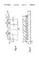
- FIG. 1is a cross-sectional view of a multichip module incorporating a high density interconnect structure having a solvent-soluble release layer between the second and third strata;
- FIG. 2is a cross-sectional view of a multichip module incorporating a high density interconnect structure having a solvent-soluble release layer between the substrate and the first stratum;
- FIG. 3is a cross-sectional view of a stack of multichip modules having a first solvent-soluble release layer used to bond together the individual modules into a stack, as well as a second solvent-soluble release layer used to bond to the stack a side stratum of high density interconnect material; and
- FIG. 4is a cross-sectional view of the edge of a stack of multichip modules having a second solvent-soluble release layer used to bond a side stratum of high density interconnect material to the stack of multichip modules.
- FIG. 5is a cross-sectional view of the edge of a multichip module, incorporating a high density interconnect structure, bonded to a base with a solvent soluble release layer.
- a multichip module 10has a substrate 11 with a plurality of chip cavities 11a formed therein, through a top surface 11b thereof.
- An integrated circuit chip 12 or another electronic componentis disposed in each chipwell 11a.
- Electronic components 12may be bonded to the substrate 11 with a layer of a thermoplastic adhesive 14; these electronic components 12 have contact pads 12a on an upper contact surface thereof 12b.
- a high density interconnect structure 16is fabricated above the chips 12 on the substrate upper surface 11b.
- a first stratum 18 of the overlying high density interconnect structure 16comprises a dielectric layer 20 supporting a patterned metallization layer 22.
- the dielectric layer 20has separate lower and upper sublayers 24 and 26, respectively, and supports the patterned metallization layer 22 which extends into contact with contact pads 12a on the substrate 11 within via holes 27 in the dielectric layer.
- the lower dielectric sublayer 24is a thermoplastic adhesive having a first glass transition temperature T g1 .
- the upper dielectric sublayer 26may be a thermoplastic material having a higher T g , but is preferably a thermoset material.
- the chip adhesivehave a glass transition temperature (T g ) which is higher than T g1 .
- T gglass transition temperature
- the upper sublayer 26 of the first dielectric layer 20should be stable over a range of temperatures above T g1 , for stability during lamination to the chips in the fabrication process. It is preferred that the upper sublayer 26 be stable to at least 100° C. above T g1 . By stable, we mean the upper sublayer 26 must have sufficient viscosity that it does not shift, stretch or otherwise change in an undesirable manner during the lamination step.
- This upper sublayer 26is preferably a thermoset film (for example, a KAPTON® film). Other materials, including thermoplastics which exhibit sufficient stability, may also be used.
- a second stratum 28 of the high density interconnect structurecomprises a second dielectric layer 30 supporting a second patterned metallization layer 32.
- the dielectric layer 30has separate lower and upper sublayers 34 and 36, respectively.
- the second lower sublayer 34is a high T g thermosetting adhesive and the upper sublayer 36 is preferably a KAPTON® resin overlay.
- Via holes 37are drilled and another patterned metallization sublayer 32 extends into via holes 37 in the dielectric layer 30 to make contact with the first metallization layer 22. If desired, selected via holes may extend through the first dielectric layer 20 as well to provide direct contact to selected contact pads 12a.
- the high T g thermosetting adhesive 34is a combination of a thermoplastic material and a thermosetting material into a freestanding, B-staged, hot melt or lamination adhesive with improved processing properties over thermosetting or thermoplastic materials alone.
- ULTEM® resinhaving a flexible polyetherimide structure
- cross-linkable epoxycreates a high T g material which is thermosetting and can be applied by hot melt application.
- Suitable curing agents for these epoxiesinclude Lewis acids, various metal cation salt curing agents, Octacat (a trademark of the General Electric Co., Waterford, Silicon Products Department), organic titanates, copper naphthenate, and many other curing agents and their equivalents known in the art. This lamination can be carried out at 200° C., still within the required processing temperature range. However, once this material, a combination of thermoplastic and thermosetting materials, is laminated (cured) the T g increases, and creates a temperature and solvent resistant second stratum.
- a third stratum of the high density interconnect structurecomprises a solvent-soluble release layer 38.
- the solvent-soluble release layer 38is a polymer which is soluble in a solvent which has no adverse effects on the portions of the multichip module 10, processed to the second stratum 28. This layer provides the ability to quickly, cleanly and easily remove any additional layers which are laminated above the solvent-soluble release layer 38.
- the polymer material of this layermust be soluble in solvents which will not attack the processed module 10, and should have a sufficiently high T g to prevent softening during processing of strata more removed from the substrate.
- the solvent-soluble release layer 38 of the present inventionmust meet several requirements. Firstly, the release layer 38 must adhere well to materials such as alumina, gallium arsenide, silicon nitride, several metals, and polyimides such as KAPTON® resin films. Secondly, the layer 38 must be compatible with the process steps inherent in the manufacturing of the high density interconnect structure. This process compatibility includes the ability to not substantially deform at temperatures of 120° C., as well as at a processing temperature of approximately 190° C. The solvent-soluble release layer 38 must also be laser ablatable or should be rendered laser ablatable in accordance with U.S.
- release layer materialis the aforementioned XU-218 polyimide, which is soluble in cyclohexanone and has a T g of 320° C.
- This material, and these release polymers in general,can be applied from solution by conventional spin and spray techniques.
- Other polymerssuch as polysulfones, polyesters, certain acrylics and other polymer blends can be used as solvent-soluble release layers.
- the fourth stratum 40 of the high density interconnect structurecomprises a fourth dielectric layer 42 supporting a fourth patterned metallization layer 44.
- the dielectric layer 42has separate lower and upper sublayers 46 and 48, respectively.
- the fourth lower dielectric sublayeris preferably a SPIE thermosetting adhesive, having a lower T g than both the T g s of the materials used for either of the first two strata 18 and 28, as well as the T g used for the solvent-soluble release layer 38.
- the fourth stratumalso comprises a third patterned metallization layer 44.
- the fourth upper dielectric sublayer 48may again be a thermoset material or a thermoplastic material and is preferably a thermoset material, or KAPTON® film. Lamination of this fourth stratum 40 is followed by via drilling which extends vias 49 through the stratum 40 and solvent-soluble release layer 38 such that the patterned metallization layer 44 will connect to the metal layer 32 of the second dielectric layer 28.
- Additional (fifth, sixth, etc.) strata of the high density interconnect structureare not shown in FIG. 1, but, if used, will be (HDI) essentially identical to the lower strata 18 and 28, except with respect to layer T g s.
- Each additional upper stratumwould comprise a dielectric layer having a thermosetting adhesive (preferably a SPIE blend) and having via holes therein, and a patterned metallization layer making contact with the patterned metallization of the next lower patterned metallization layer through the via holes.
- Other stratacan be added in accordance with the above description.
- various metallization layers 22, 32, 44will carry power, ground, and at least one set of signal conductors.
- the benefit of this structureis that, after fabrication through the first two layers (e.g. including ground and power conductor layers) the module can be pre-tested to ensure that all chips are working properly. Then, after the upper strata are laminated, the module can be finally tested and any detected problem is ensured to be in the top strata and, as such, the module incorporating the solvent-soluble release layer 38 can be reworked.
- the relatively high T g s of the first two stratawill prevent any shifting of material if any reworking is necessary. There are two modes of reworking the module.
- the first modeinvolves heating the module to 225° C., and peeling off the KAPTON® film of the stratum directly above the release layer.
- the SPIE adhesive layeris soft at this temperature and allows for separation of the KAPTON® film overlay.
- the substrateis partially covered with residual SPIE adhesive layer (insoluble) on top of the release layer 38.
- the modulecan be immersed in an appropriate solvent to dissolve the release layer and hence float off the insoluble polyimide/epoxy. Upon rinsing, a clean module comprising the first two strata 18 and 28 are revealed. Two new strata 38 and 40 can be added to the module for very quick repair.
- the second and alternative removal approachis to just soak the laminated part in an appropriate solvent to dissolve the release layer and float off the KAPTON® resin film and crosslinked polyimide/epoxy. This reworkability provides for pretesting of the power and ground layers prior to additional strata being added and quick design change of the additional signal layers.
- the SPIE crosslinking copolymer blend adhesive materials used as the lower dielectric sublayer in the fourth and higher strataare selected so that these adhesive materials become set at a low enough temperature that curing the adhesive materials has no adverse effect on the high density interconnect structure or the electronic components being connected thereby. Correct selection of the curing properties of the adhesive materials allows the structure to be fabricated and, if need be, disassembled and reassembled without an adverse effect on the electronic components being interconnected.
- a solvent-soluble release layeris disposed between the first stratum of the high density interconnect structure and the chips mounted in the substrate.
- the adhesive used for the first dielectric layer, and all other dielectric layerscan be a thermoset adhesive. This allows all layers to be laminated at temperatures 200° C. or below.
- This low temperature (HDI) structure 10comprises a substrate 11 having cavities 11a in the upper surface thereof 11b in which integrated chips 12 or other electronic components are disposed. For many high density structures, these electronic components are bonded to the substrate with a thermoplastic adhesive 14. These electronic components have contact pads 12a on an upper contact surface thereof 12b.
- a first stratum 38 of the overlying high density interconnect structure 16comprises a solvent-soluble release layer. This layer is a polymer material which must be soluble in solvents which will not attack the processed module at this point, and should have a sufficiently high T g to prevent softening during additional upper layer processing.
- polyimide XU-218is soluble in cyclohexanone and has a T g value of 320° C.
- the solvent-soluble release polymeris sprayed or spin coated as layer 38, and baked to remove solvent.
- a second stratum of the high density interconnect structure 16comprises a first dielectric layer 20 supporting a first patterned metallization layer 22.
- the dielectric layerhas separate lower and upper sublayers 24 and 26, respectively.
- the lower sublayer 24is again a thermoset material and is preferably a SPIE copolymer blend. Since the material of this lower sublayer 24 is a thermosetting polymer, and therefore changes solubility properties, as well as its T g value, upon curing, laminating multiple layers does not affect lower layers.
- the upper sublayer 26may again be a thermoset material or a thermoplastic material and is preferably a thermoset material (e.g., KAPTON® resin film).
- the patterned metallization 22extends into via holes 27 in the dielectric layer 20 to make electrical contact with the contact pads 12a.
- a third stratum of the high density interconnect structure 16comprises a dielectric layer 30 supporting a patterned metallization layer 32.
- the dielectric layer 30has separate lower and upper sublayers 34 and 36.
- the third lower sublayer 34is preferably an SPIE crosslinking copolymer blend.
- the third upper dielectric sublayer 36may again be a thermoset material or a thermoplastic material and is preferably a thermoset KAPTON® film.
- FIG. 3shows another aspect of the present invention, specifically, an assembly 100 of stacked and joined multichip modules 110, each module 110 incorporating a high density interconnect structure 116.
- the assembly 100is a 3D-HDI structure.
- Each of the modules 110has a substrate 114 which has a plurality of metal edge connection pads 112; at each pad the metallization is wrapped from the top substrate surface 114a around to the substrate edge 114b.
- the stacked modules 110are joined to one another by use of another solvent-soluble release layer 118 located between facing surfaces of each adjacent pair of modules.
- Edge connection pad metallization 112is electrically connected to the high density interconnect structure 116 of each module 110.
- the high density interconnect structure 116comprises metal distribution lines that extend to the integrated circuits and other electronic component chips mounted in the substrate 114, in manner as described above.
- the metal edge connection pads 112can be fabricated by a variety of different techniques using a variety of different metals explicitly described in U.S. Pat. No. 5,107,586, entitled "Method for Interconnecting a Stack of Integrated Circuits at a Very High Density" herein incorporated in its entirety by reference.
- the adhesive used to bond the separate modules 110 together into assembly 100is a solvent-soluble release layer 118 soluble in an appropriate solvent.
- the HDI substratesare stacked in an alignment jig, with their edges substantially parallel to one another with aligned common edges, and laminated together. The exact method for assembling the 3D-HDI structures is taught in U.S. Pat. No. 5,107,586, cited above.
- a solvent-soluble release layer 120is disposed over the edge of the module assembly 100.
- the solvent-soluble release layer 120may be applied by spray techniques after the individual modules have been stacked.
- a side stratum 126, disposed over the solvent-soluble release layer 120has a dielectric layer 123, which is comprised of upper sublayer 122 and lower sublayer 121, respectively.
- the upper dielectric sublayer 122is preferably a KAPTON® film and is bonded to the solvent-soluble release layer 120 by an adhesive 121.
- the release layerprevents the epoxy from crosslinking to the substrate material.
- the release layer 120allows the adhesive 121 to be removed along with the dissolution of the release layer 120.
- the adhesive 121can be either a thermosetting material or a thermoplastic material, but is preferably thermosetting material such as a SPIE blend.
- the dielectric layer 123has via holes 128 disposed both through the dielectric layer 122 and the release layer 120, in alignment with at least some of the metal edge connection pads 112.
- a patterned metallization layer 124fills these via holes 128 and makes electrical contact with associated ones of the metal edge connection pads 112.
- An important advantage of this inventionis the repairability of any interconnected module 110 of the stacked HDI module assembly 100.
- heatis applied to the side of the assembly 100 having release layer 120, so as to raise the temperature of the side stratum 126 above the T g of the adhesive 121 on the edges of the KAPTON® resin layer 123 and allow peeling off of the KAPTON® resin layer 123.
- the 3D-HDI stack 100can be soaked in an appropriate solvent thereby making the stacked substrates separate and accessible.
- the solvent-soluble release layer 120may be the same as the solvent-soluble release layer 118 or it may be different, but is preferably different.
- the solvent used to remove the release layer 120will have no effect on the solvent-soluble release layer 118 within each module, nor will it affect any other portion of the module.
- the stackneed not be heated and may simply be immersed in a selected solvent to dissolve the solvent-soluble release layer 120 directly and thereby allowing the stacked substrates to be separated and made individually accessible.
- the assembly 100is soaked in another solvent which will dissolve the release layer 118 which holds the assembly together. Upon dissolution of the release layer 118, any substrate may be removed easily and a replacement HDI substrate is then inserted into the stack 100 and the stack 100 is adhesively bonded as described above.
- the interconnection of a repaired stack 100'proceeds exactly the same as when creating an interconnected stacked module 100.
- the ability to simply remove the dielectric material 123 and patterned metallization layer 124 from the side of a module assembly 100provides the additional feature of being able to redesign the interconnection scheme.
- FIG. 5shows another aspect of the present invention.
- a solvent soluble release layercan be used to bond together a multichip module 110 and a base 150.
- the release layer 120is used with an epoxy 160 to ensure an adequate bond between the multichip module and the release layer.
- the module 110 and the base 150can be separated simply by immersing the solvent soluble release layer 120 in an appropriate solvent.
- the base 150typically will be a SEM-E board base.
- a multilayer interconnect structurecan be fabricated using the release layer between the first overlay layer and the chips on the substrate.
- the following process flowcan be conducted.
- a polysulfone layeris coated on the chips and substrate, baked to remove the solvent, and a first layer lamination is applied using the SPIE adhesive with 1 mil thick KAPTON® film.
- An argon ion laseris used to drill via holes in the dielectric overlay to bond pads on the chip.
- thin Ti and Cu layersare sputtered (1000 A for each layer) and a 4 um thick Cu film is electroplated and then another sputtered Ti layer (1000 A) is applied to provide metal over the entire surface.
- a photoresistis coated over the metal, exposed with the same argon ion laser and developed to open up regions of the metal surface which are then wet etched to give a metal interconnect pattern on the dielectric surface connected to the bond pads.
- the remaining resistis removed, and another layer of KAPTON® film is laminated with the same SPIE adhesive. Vias are again drilled, metal deposited as described above, and patterned to give another layer of interconnect. Additional layers of dielectric and metal can be applied if required to complete the interconnect structure. The entire processing sequence is done at temperatures below 200° C.
- the completed moduleis soaked for 16 hrs in acetophenone to dissolve the polysulfone release layer and allow the interconnect structure to be separated from the chips mounted on the substrate.
- the metallization layer bonded to the chipsis broken as the interconnect structure is removed, leaving a small amount of Ti/Cu/Ti which must be removed. This can be accomplished by dipping in dilute nitric acid for a few minutes, followed by a high pressure deionized water scrub.
- An alternate method of removalinvolves heating the completed module fabricated with the above sequence to 200° C. to soften the SPIE adhesive and peal the entire interconnect off the chips and substrate leaving the release layer exposed on the surface. The part is then soaked in acetophenone for 2 hrs at 50° C., to remove the release polymer and any residual SPIE still remaining. The release polymer is cleaned off in shorter time in this approach because the entire surfaces of the release layer is in contact with the solvent.
- a release layerwas formed of a 10% by weight solution of XU-218 polyimide (available from Ciba Geigy Corp.) in cyclohexanone; this solution was coated as a film over a silicon chip mounted in a chip well on an alumina substrate. The release layer film was baked at 250° C. to remove the solvent (resulting in a thin polymer coating thickness of about 5 um). A KAPTON® resin film was then laminated using the SPIE blend as an adhesive. The lamination was carried out at 190° C.
- a void-free lamination, of the KAPTON® film, over the release layer, over the chip and substratewas obtained and adhesion measurements showed a pull strength of greater than 7 lbs/in, indicative of excellent adhesion.
- the structurewas then soaked in cyclohexanone for 16 hrs which resulted in dissolution of the release layer and removal of the overlay film from substrate and the chip mounted thereon.
- a film with the following compositionwas spin coated on KAPTON® film and baked at 100oC to remove the solvent:
- the KAPTON® film with the dried adhesivewas then laminated in vacuum onto alumina by heating to 200° C. and holding under pressure at that temperature for 1/2 hr.
- the adhesion of the KAPTON® film to the alumina substratewas measured to be 5 lbs.
- Free standing films of XU-218/epoxy blends and ULTEM®/epoxy blendswere prepared by coating on teflon and baking for 10 min at 100° C., 20 min at 150° C. and 30 min at 200° C.
- the filmscould readily be peeled off the teflon and their melt flow characteristics were characterized by measuring the cut-thru temperatures. This was achieved by placing the film between two copper wires and then heating at a controlled rate. The point at which the polymer flowed causing the two wires to make contact was defined as the cut-thru temperature.
- the same testwas also run on the currently used siloxane-polyimide/epoxy material giving cut thru values as shown below:
- the films of ULTEM®/epoxy blend or XU-218/epoxy blendwere found to have improved thermal stability over the SPIE blends.
Landscapes
- Engineering & Computer Science (AREA)
- Computer Hardware Design (AREA)
- Microelectronics & Electronic Packaging (AREA)
- Power Engineering (AREA)
- Physics & Mathematics (AREA)
- Condensed Matter Physics & Semiconductors (AREA)
- General Physics & Mathematics (AREA)
- Manufacturing & Machinery (AREA)
- Ceramic Engineering (AREA)
- Production Of Multi-Layered Print Wiring Board (AREA)
Abstract
Description
______________________________________ 15 g XU-218 polyimide (Ciba-Geigy) 60 g Cyclohexanone 22.5 g CY179 epoxy resin (Ciba-Geigy) 6 g Xylene 0.225 g Octacat-TM (1 wt % of epoxy) 0.5625 g Copper Naphthenate (solution equivalent to 1 wt % of epoxy) ______________________________________
______________________________________ Sample Cut thru Temperatures ______________________________________ SPI/epoxy blend 150° C. ULTEM ®/epoxy blend 190° C. XU-218 epoxy blend 250° C. ______________________________________
Claims (17)
Priority Applications (1)
| Application Number | Priority Date | Filing Date | Title |
|---|---|---|---|
| US08/225,876US5434751A (en) | 1994-04-11 | 1994-04-11 | Reworkable high density interconnect structure incorporating a release layer |
Applications Claiming Priority (1)
| Application Number | Priority Date | Filing Date | Title |
|---|---|---|---|
| US08/225,876US5434751A (en) | 1994-04-11 | 1994-04-11 | Reworkable high density interconnect structure incorporating a release layer |
Publications (1)
| Publication Number | Publication Date |
|---|---|
| US5434751Atrue US5434751A (en) | 1995-07-18 |
Family
ID=22846621
Family Applications (1)
| Application Number | Title | Priority Date | Filing Date |
|---|---|---|---|
| US08/225,876Expired - LifetimeUS5434751A (en) | 1994-04-11 | 1994-04-11 | Reworkable high density interconnect structure incorporating a release layer |
Country Status (1)
| Country | Link |
|---|---|
| US (1) | US5434751A (en) |
Cited By (89)
| Publication number | Priority date | Publication date | Assignee | Title |
|---|---|---|---|---|
| DE19642488A1 (en)* | 1996-10-15 | 1998-04-16 | Bernd Klose | Thin-layer circuit board for e.g. chip card |
| US5897337A (en)* | 1994-09-30 | 1999-04-27 | Nec Corporation | Process for adhesively bonding a semiconductor chip to a carrier film |
| EP0923130A1 (en)* | 1997-12-12 | 1999-06-16 | ELA MEDICAL (Société anonyme) | Electronic circuit, in particular for implantable active medical device, like a heart stimulator or defibrillator, and its manufacturing method |
| US5998876A (en)* | 1997-12-30 | 1999-12-07 | International Business Machines Corporation | Reworkable thermoplastic hyper-branched encapsulant |
| US6015607A (en)* | 1995-06-28 | 2000-01-18 | Fraivillig Materials Company | Flexible laminates and method of making the laminates |
| US6085413A (en)* | 1998-02-02 | 2000-07-11 | Ford Motor Company | Multilayer electrical interconnection device and method of making same |
| US6111323A (en)* | 1997-12-30 | 2000-08-29 | International Business Machines Corporation | Reworkable thermoplastic encapsulant |
| US6127633A (en)* | 1995-04-28 | 2000-10-03 | Victor Company Of Japan, Ltd. | Multilayer print circuit board having a blind hole in an insulation layer with a roughened surface formed by application of an oxidizing agent and method of production |
| EP1041620A2 (en)* | 1999-04-02 | 2000-10-04 | Interuniversitair Microelektronica Centrum Vzw | Method of transferring ultrathin substrates and application of the method to the manufacture of a multi-layer thin film device |
| US6148512A (en)* | 1996-04-22 | 2000-11-21 | Motorola, Inc. | Method for attaching an electronic device |
| US6188129B1 (en)* | 1997-03-24 | 2001-02-13 | Hyundai Electronics Industries Co., Ltd. | Stacked semiconductor chip package having external terminal pads and stackable chips having a protection layer |
| US6239482B1 (en) | 1999-06-21 | 2001-05-29 | General Electric Company | Integrated circuit package including window frame |
| US6294743B1 (en)* | 1995-04-28 | 2001-09-25 | Victor Company Of Japan, Ltd. | Multilayer print circuit board and the production method of the multilayer print circuit board |
| US6306688B1 (en)* | 1999-04-28 | 2001-10-23 | Teravicta Technologies, Inc. | Method of reworkably removing a fluorinated polymer encapsulant |
| US6332988B1 (en) | 1999-06-02 | 2001-12-25 | International Business Machines Corporation | Rework process |
| US20020109232A1 (en)* | 1998-12-21 | 2002-08-15 | Mou-Shiung Lin | Chip structure and process for forming the same |
| US6468638B2 (en)* | 1999-03-16 | 2002-10-22 | Alien Technology Corporation | Web process interconnect in electronic assemblies |
| US6500750B1 (en)* | 1999-04-05 | 2002-12-31 | Motorola, Inc. | Semiconductor device and method of formation |
| US6548767B1 (en)* | 1999-12-16 | 2003-04-15 | Lg Electronics, Inc. | Multi-layer printed circuit board having via holes formed from both sides thereof |
| US20030122229A1 (en)* | 2001-10-31 | 2003-07-03 | Bakir Muhannad S. | Devices having compliant wafer-level packages with pillars and methods of fabrication |
| US20030122244A1 (en)* | 2001-12-31 | 2003-07-03 | Mou-Shiung Lin | Integrated chip package structure using metal substrate and method of manufacturing the same |
| US20030231474A1 (en)* | 2002-06-14 | 2003-12-18 | Boggs David W. | PCB method and apparatus for producing landless interconnects |
| US20040014317A1 (en)* | 2000-09-25 | 2004-01-22 | Hajime Sakamoto | Semiconductor element, method of manufacturing semiconductor element, multi-layer printed circuit board, and method of manufacturing multi-layer printed circuit board |
| US20040043533A1 (en)* | 2002-08-27 | 2004-03-04 | Chua Swee Kwang | Multi-chip wafer level system packages and methods of forming same |
| US6717063B2 (en)* | 1997-09-17 | 2004-04-06 | Telefonaktiebolaget Lm Ericsson (Publ) | Multi-layer circuit board with supporting layers of different materials |
| US6746898B2 (en)* | 2001-12-31 | 2004-06-08 | Megic Corporation | Integrated chip package structure using silicon substrate and method of manufacturing the same |
| US20040155325A1 (en)* | 2000-10-04 | 2004-08-12 | Intel Corporation | Die-in heat spreader microelectronic package |
| US20040157361A1 (en)* | 2003-02-12 | 2004-08-12 | Micron Technology, Inc. | Semiconductor substrate for build-up packages |
| US20040168825A1 (en)* | 2000-02-25 | 2004-09-02 | Hajime Sakamoto | Multilayer printed circuit board and multilayer printed circuit board manufacturing method |
| US20040183182A1 (en)* | 2002-01-23 | 2004-09-23 | Susan Swindlehurst | Apparatus incorporating small-feature-size and large-feature-size components and method for making same |
| US20040188531A1 (en)* | 2003-03-24 | 2004-09-30 | Gengel Glenn W. | RFID tags and processes for producing RFID tags |
| US20050017271A1 (en)* | 1999-03-11 | 2005-01-27 | Shinko Electric Industries Co.,Inc. | Multilayered substrate for semiconductor device and method of manufacturing same |
| US6881611B1 (en) | 1996-07-12 | 2005-04-19 | Fujitsu Limited | Method and mold for manufacturing semiconductor device, semiconductor device and method for mounting the device |
| US20050087859A1 (en)* | 2003-08-28 | 2005-04-28 | Advanced Semiconductor Engineering, Inc. | Semiconductor chip package and method for manufacturing the same |
| US20050205291A1 (en)* | 2004-03-19 | 2005-09-22 | Yoshihisa Yamashita | Flexible substrate having interlaminar junctions, and process for producing the same |
| US20050270757A1 (en)* | 2001-05-31 | 2005-12-08 | Credelle Thomas L | Electronic devices with small functional elements supported on a carrier |
| US20060109123A1 (en)* | 2004-11-22 | 2006-05-25 | Curt Carrender | Radio frequency identification (RFID) tag for an item having a conductive layer included or attached |
| US20070158861A1 (en)* | 2003-05-14 | 2007-07-12 | Siliconware Precision Industries Co., Ltd. | Method for fabricating semiconductor package with build-up layers formed on chip |
| US20070273033A1 (en)* | 1998-12-21 | 2007-11-29 | Mou-Shiung Lin | Top layers of metal for high performance IC's |
| US20080048328A1 (en)* | 2001-12-13 | 2008-02-28 | Megica Corporation | Chip structure and process for forming the same |
| US20080108171A1 (en)* | 2006-09-20 | 2008-05-08 | Rogers John A | Release strategies for making transferable semiconductor structures, devices and device components |
| US20080130254A1 (en)* | 2006-12-04 | 2008-06-05 | Samsung Electronics Co., Ltd. | Electronic device with reworkable electronic component, method of fabricating the electronic device and method of reworking the electronic component |
| US20080136034A1 (en)* | 1998-12-21 | 2008-06-12 | Megica Corporation | Chip structure and process for forming the same |
| US20080318055A1 (en)* | 2007-06-21 | 2008-12-25 | General Electric Company | Recoverable electronic component |
| US20080314867A1 (en)* | 2007-06-21 | 2008-12-25 | General Electric Company | Method of making demountable interconnect structure |
| US20080318054A1 (en)* | 2007-06-21 | 2008-12-25 | General Electric Company | Low-temperature recoverable electronic component |
| US20080318027A1 (en)* | 2007-06-21 | 2008-12-25 | General Electric Company | Demountable interconnect structure |
| US20080313894A1 (en)* | 2007-06-21 | 2008-12-25 | General Electric Company | Method for making an interconnect structure and low-temperature interconnect component recovery process |
| US20080318413A1 (en)* | 2007-06-21 | 2008-12-25 | General Electric Company | Method for making an interconnect structure and interconnect component recovery process |
| US20090011542A1 (en)* | 2001-03-30 | 2009-01-08 | Megica Corporation | Structure and manufactruing method of chip scale package |
| US20090146287A1 (en)* | 1996-12-03 | 2009-06-11 | Oki Electric Industry Co., Ltd. | Semiconductor device having a chip-size package |
| EP2184774A1 (en)* | 2008-11-05 | 2010-05-12 | General Electric Company | Low-temperature recoverable electronic component |
| EP2184773A1 (en)* | 2008-11-05 | 2010-05-12 | General Electric Company | Recoverable electronic component |
| US20100283069A1 (en)* | 2007-01-17 | 2010-11-11 | John Rogers | Optical systems fabricated by printing-based assembly |
| US7838892B2 (en) | 2004-04-29 | 2010-11-23 | Osram Opto Semiconductors Gmbh | Optoelectronic semiconductor chip and method for forming a contact structure for making electrical contact with an optoelectronic semiconductor chip |
| US20100317132A1 (en)* | 2009-05-12 | 2010-12-16 | Rogers John A | Printed Assemblies of Ultrathin, Microscale Inorganic Light Emitting Diodes for Deformable and Semitransparent Displays |
| US7982296B2 (en) | 2004-06-04 | 2011-07-19 | The Board Of Trustees Of The University Of Illinois | Methods and devices for fabricating and assembling printable semiconductor elements |
| US8039847B2 (en) | 2004-06-04 | 2011-10-18 | The Board Of Trustees Of The University Of Illinois | Printable semiconductor structures and related methods of making and assembling |
| US20120042513A1 (en)* | 2008-06-25 | 2012-02-23 | Samsung Electro-Mechanics Co., Ltd. | Manufacturing method of printed circuit board embedded chip |
| US20120304458A1 (en)* | 2011-03-17 | 2012-12-06 | Ibiden Co., Ltd. | Method for manufacturing multilayer printed wiring board |
| US8372726B2 (en) | 2008-10-07 | 2013-02-12 | Mc10, Inc. | Methods and applications of non-planar imaging arrays |
| US8389862B2 (en) | 2008-10-07 | 2013-03-05 | Mc10, Inc. | Extremely stretchable electronics |
| US8471361B2 (en) | 2001-12-31 | 2013-06-25 | Megica Corporation | Integrated chip package structure using organic substrate and method of manufacturing the same |
| US8492870B2 (en) | 2002-01-19 | 2013-07-23 | Megica Corporation | Semiconductor package with interconnect layers |
| US8536667B2 (en) | 2008-10-07 | 2013-09-17 | Mc10, Inc. | Systems, methods, and devices having stretchable integrated circuitry for sensing and delivering therapy |
| US8535976B2 (en) | 2001-12-31 | 2013-09-17 | Megica Corporation | Method for fabricating chip package with die and substrate |
| US8666471B2 (en) | 2010-03-17 | 2014-03-04 | The Board Of Trustees Of The University Of Illinois | Implantable biomedical devices on bioresorbable substrates |
| US8886334B2 (en) | 2008-10-07 | 2014-11-11 | Mc10, Inc. | Systems, methods, and devices using stretchable or flexible electronics for medical applications |
| US8934965B2 (en) | 2011-06-03 | 2015-01-13 | The Board Of Trustees Of The University Of Illinois | Conformable actively multiplexed high-density surface electrode array for brain interfacing |
| US9159635B2 (en) | 2011-05-27 | 2015-10-13 | Mc10, Inc. | Flexible electronic structure |
| WO2015160624A1 (en)* | 2014-04-17 | 2015-10-22 | Massachusetts Institute Of Technology | Printed circuit board assembly with air dielectric |
| US9171794B2 (en) | 2012-10-09 | 2015-10-27 | Mc10, Inc. | Embedding thin chips in polymer |
| US20150380369A1 (en)* | 2013-09-30 | 2015-12-31 | Nantong Fujitsu Microelectronics Co., Ltd | Wafer packaging structure and packaging method |
| US20160044798A1 (en)* | 2013-06-18 | 2016-02-11 | Murata Manufacturing Co., Ltd. | Method of manufacturing resin multilayer substrate |
| US9289132B2 (en) | 2008-10-07 | 2016-03-22 | Mc10, Inc. | Catheter balloon having stretchable integrated circuitry and sensor array |
| US9442285B2 (en) | 2011-01-14 | 2016-09-13 | The Board Of Trustees Of The University Of Illinois | Optical component array having adjustable curvature |
| US9554484B2 (en) | 2012-03-30 | 2017-01-24 | The Board Of Trustees Of The University Of Illinois | Appendage mountable electronic devices conformable to surfaces |
| US9691873B2 (en) | 2011-12-01 | 2017-06-27 | The Board Of Trustees Of The University Of Illinois | Transient devices designed to undergo programmable transformations |
| US9723122B2 (en) | 2009-10-01 | 2017-08-01 | Mc10, Inc. | Protective cases with integrated electronics |
| US9765934B2 (en) | 2011-05-16 | 2017-09-19 | The Board Of Trustees Of The University Of Illinois | Thermally managed LED arrays assembled by printing |
| US9936574B2 (en) | 2009-12-16 | 2018-04-03 | The Board Of Trustees Of The University Of Illinois | Waterproof stretchable optoelectronics |
| US10375834B1 (en)* | 2013-08-27 | 2019-08-06 | Flextronics Ap, Llc. | 3D printing with components embedded |
| US10441185B2 (en) | 2009-12-16 | 2019-10-15 | The Board Of Trustees Of The University Of Illinois | Flexible and stretchable electronic systems for epidermal electronics |
| US10449729B1 (en) | 2015-12-03 | 2019-10-22 | Multek Technologies Ltd. | 3D printed fiber optics |
| US10918298B2 (en) | 2009-12-16 | 2021-02-16 | The Board Of Trustees Of The University Of Illinois | High-speed, high-resolution electrophysiology in-vivo using conformal electronics |
| US10925543B2 (en) | 2015-11-11 | 2021-02-23 | The Board Of Trustees Of The University Of Illinois | Bioresorbable silicon electronics for transient implants |
| US11029198B2 (en) | 2015-06-01 | 2021-06-08 | The Board Of Trustees Of The University Of Illinois | Alternative approach for UV sensing |
| US11118965B2 (en) | 2015-06-01 | 2021-09-14 | The Board Of Trustees Of The University Of Illinois | Miniaturized electronic systems with wireless power and near-field communication capabilities |
| US11824013B2 (en) | 2019-08-15 | 2023-11-21 | Intel Corporation | Package substrate with reduced interconnect stress |
Citations (6)
| Publication number | Priority date | Publication date | Assignee | Title |
|---|---|---|---|---|
| US4783695A (en)* | 1986-09-26 | 1988-11-08 | General Electric Company | Multichip integrated circuit packaging configuration and method |
| US4859512A (en)* | 1986-08-01 | 1989-08-22 | The Excello Specialty Company | Transfer adhesive sandwich for applying adhesive to substrates |
| US4933042A (en)* | 1986-09-26 | 1990-06-12 | General Electric Company | Method for packaging integrated circuit chips employing a polymer film overlay layer |
| US5073814A (en)* | 1990-07-02 | 1991-12-17 | General Electric Company | Multi-sublayer dielectric layers |
| US5157589A (en)* | 1990-07-02 | 1992-10-20 | General Electric Company | Mutliple lamination high density interconnect process and structure employing thermoplastic adhesives having sequentially decreasing TG 's |
| US5161093A (en)* | 1990-07-02 | 1992-11-03 | General Electric Company | Multiple lamination high density interconnect process and structure employing a variable crosslinking adhesive |
- 1994
- 1994-04-11USUS08/225,876patent/US5434751A/ennot_activeExpired - Lifetime
Patent Citations (6)
| Publication number | Priority date | Publication date | Assignee | Title |
|---|---|---|---|---|
| US4859512A (en)* | 1986-08-01 | 1989-08-22 | The Excello Specialty Company | Transfer adhesive sandwich for applying adhesive to substrates |
| US4783695A (en)* | 1986-09-26 | 1988-11-08 | General Electric Company | Multichip integrated circuit packaging configuration and method |
| US4933042A (en)* | 1986-09-26 | 1990-06-12 | General Electric Company | Method for packaging integrated circuit chips employing a polymer film overlay layer |
| US5073814A (en)* | 1990-07-02 | 1991-12-17 | General Electric Company | Multi-sublayer dielectric layers |
| US5157589A (en)* | 1990-07-02 | 1992-10-20 | General Electric Company | Mutliple lamination high density interconnect process and structure employing thermoplastic adhesives having sequentially decreasing TG 's |
| US5161093A (en)* | 1990-07-02 | 1992-11-03 | General Electric Company | Multiple lamination high density interconnect process and structure employing a variable crosslinking adhesive |
Non-Patent Citations (1)
| Title |
|---|
| IBM Technical Disclosure Bulletin Interconnection Alignment Multichip Module by Balderes et al. vol. 15 No. 10 Mar. 1973 (p. 3024).* |
Cited By (247)
| Publication number | Priority date | Publication date | Assignee | Title |
|---|---|---|---|---|
| US5897337A (en)* | 1994-09-30 | 1999-04-27 | Nec Corporation | Process for adhesively bonding a semiconductor chip to a carrier film |
| US6127633A (en)* | 1995-04-28 | 2000-10-03 | Victor Company Of Japan, Ltd. | Multilayer print circuit board having a blind hole in an insulation layer with a roughened surface formed by application of an oxidizing agent and method of production |
| US6294744B1 (en)* | 1995-04-28 | 2001-09-25 | Victor Company Of Japan, Ltd. | Multilayer print circuit board and the production method of the multilayer print circuit board |
| US6294743B1 (en)* | 1995-04-28 | 2001-09-25 | Victor Company Of Japan, Ltd. | Multilayer print circuit board and the production method of the multilayer print circuit board |
| US6015607A (en)* | 1995-06-28 | 2000-01-18 | Fraivillig Materials Company | Flexible laminates and method of making the laminates |
| US6148512A (en)* | 1996-04-22 | 2000-11-21 | Motorola, Inc. | Method for attaching an electronic device |
| US6881611B1 (en) | 1996-07-12 | 2005-04-19 | Fujitsu Limited | Method and mold for manufacturing semiconductor device, semiconductor device and method for mounting the device |
| DE19642488A1 (en)* | 1996-10-15 | 1998-04-16 | Bernd Klose | Thin-layer circuit board for e.g. chip card |
| US20090146287A1 (en)* | 1996-12-03 | 2009-06-11 | Oki Electric Industry Co., Ltd. | Semiconductor device having a chip-size package |
| US8154124B2 (en)* | 1996-12-03 | 2012-04-10 | Oki Electric Industry Co., Ltd. | Semiconductor device having a chip-size package |
| US6188129B1 (en)* | 1997-03-24 | 2001-02-13 | Hyundai Electronics Industries Co., Ltd. | Stacked semiconductor chip package having external terminal pads and stackable chips having a protection layer |
| US6717063B2 (en)* | 1997-09-17 | 2004-04-06 | Telefonaktiebolaget Lm Ericsson (Publ) | Multi-layer circuit board with supporting layers of different materials |
| US6256206B1 (en) | 1997-12-12 | 2001-07-03 | Ela Medical S.A. | Electronic circuit for an active implantable medical device and method of manufacture |
| FR2772516A1 (en)* | 1997-12-12 | 1999-06-18 | Ela Medical Sa | ELECTRONIC CIRCUIT, IN PARTICULAR FOR AN ACTIVE IMPLANTABLE MEDICAL DEVICE SUCH AS A CARDIAC STIMULATOR OR DEFIBRILLATOR, AND ITS MANUFACTURING METHOD |
| EP0923130A1 (en)* | 1997-12-12 | 1999-06-16 | ELA MEDICAL (Société anonyme) | Electronic circuit, in particular for implantable active medical device, like a heart stimulator or defibrillator, and its manufacturing method |
| US6111323A (en)* | 1997-12-30 | 2000-08-29 | International Business Machines Corporation | Reworkable thermoplastic encapsulant |
| US5998876A (en)* | 1997-12-30 | 1999-12-07 | International Business Machines Corporation | Reworkable thermoplastic hyper-branched encapsulant |
| US6326237B1 (en)* | 1997-12-30 | 2001-12-04 | International Business Machines Corporation | Reworkable thermoplastic hyper-branched encapsulant |
| US6085413A (en)* | 1998-02-02 | 2000-07-11 | Ford Motor Company | Multilayer electrical interconnection device and method of making same |
| US8471384B2 (en) | 1998-12-21 | 2013-06-25 | Megica Corporation | Top layers of metal for high performance IC's |
| US7906422B2 (en) | 1998-12-21 | 2011-03-15 | Megica Corporation | Chip structure and process for forming the same |
| US7863654B2 (en) | 1998-12-21 | 2011-01-04 | Megica Corporation | Top layers of metal for high performance IC's |
| US20070284752A1 (en)* | 1998-12-21 | 2007-12-13 | Mou-Shiung Lin | Top layers of metal for high performance IC's |
| US8531038B2 (en) | 1998-12-21 | 2013-09-10 | Megica Corporation | Top layers of metal for high performance IC's |
| US7884479B2 (en) | 1998-12-21 | 2011-02-08 | Megica Corporation | Top layers of metal for high performance IC's |
| US20070281458A1 (en)* | 1998-12-21 | 2007-12-06 | Mou-Shiung Lin | Top layers of metal for high performance IC's |
| US20070278691A1 (en)* | 1998-12-21 | 2007-12-06 | Mou-Shiung Lin | Top layers of metal for high performance IC's |
| US8415800B2 (en) | 1998-12-21 | 2013-04-09 | Megica Corporation | Top layers of metal for high performance IC's |
| US20020109232A1 (en)* | 1998-12-21 | 2002-08-15 | Mou-Shiung Lin | Chip structure and process for forming the same |
| US20070278686A1 (en)* | 1998-12-21 | 2007-12-06 | Mou-Shiung Lin | Top layers of metal for high performance IC's |
| US6756295B2 (en)* | 1998-12-21 | 2004-06-29 | Megic Corporation | Chip structure and process for forming the same |
| US20070284751A1 (en)* | 1998-12-21 | 2007-12-13 | Mou-Shiung Lin | Top layers of metal for high performance IC's |
| US20070273033A1 (en)* | 1998-12-21 | 2007-11-29 | Mou-Shiung Lin | Top layers of metal for high performance IC's |
| US7906849B2 (en) | 1998-12-21 | 2011-03-15 | Megica Corporation | Chip structure and process for forming the same |
| US20070284753A1 (en)* | 1998-12-21 | 2007-12-13 | Mou-Shiung Lin | Top layers of metal for high performance IC's |
| US7470988B2 (en) | 1998-12-21 | 2008-12-30 | Megica Corporation | Chip structure and process for forming the same |
| US8022545B2 (en) | 1998-12-21 | 2011-09-20 | Megica Corporation | Top layers of metal for high performance IC's |
| US7915157B2 (en) | 1998-12-21 | 2011-03-29 | Megica Corporation | Chip structure and process for forming the same |
| US7999384B2 (en) | 1998-12-21 | 2011-08-16 | Megica Corporation | Top layers of metal for high performance IC's |
| US20080136034A1 (en)* | 1998-12-21 | 2008-06-12 | Megica Corporation | Chip structure and process for forming the same |
| US20050017271A1 (en)* | 1999-03-11 | 2005-01-27 | Shinko Electric Industries Co.,Inc. | Multilayered substrate for semiconductor device and method of manufacturing same |
| US7763809B2 (en)* | 1999-03-11 | 2010-07-27 | Shink Electric Industries Co., Inc. | Multilayered substrate for semiconductor device and method of manufacturing same |
| US6468638B2 (en)* | 1999-03-16 | 2002-10-22 | Alien Technology Corporation | Web process interconnect in electronic assemblies |
| US7425467B2 (en) | 1999-03-16 | 2008-09-16 | Alien Technology Corporation | Web process interconnect in electronic assemblies |
| US7288432B2 (en) | 1999-03-16 | 2007-10-30 | Alien Technology Corporation | Electronic devices with small functional elements supported on a carrier |
| US7070851B2 (en)* | 1999-03-16 | 2006-07-04 | Alien Technology Corporation | Web process interconnect in electronic assemblies |
| EP1041620A2 (en)* | 1999-04-02 | 2000-10-04 | Interuniversitair Microelektronica Centrum Vzw | Method of transferring ultrathin substrates and application of the method to the manufacture of a multi-layer thin film device |
| US6500750B1 (en)* | 1999-04-05 | 2002-12-31 | Motorola, Inc. | Semiconductor device and method of formation |
| US6306688B1 (en)* | 1999-04-28 | 2001-10-23 | Teravicta Technologies, Inc. | Method of reworkably removing a fluorinated polymer encapsulant |
| US6332988B1 (en) | 1999-06-02 | 2001-12-25 | International Business Machines Corporation | Rework process |
| US6239482B1 (en) | 1999-06-21 | 2001-05-29 | General Electric Company | Integrated circuit package including window frame |
| US6548767B1 (en)* | 1999-12-16 | 2003-04-15 | Lg Electronics, Inc. | Multi-layer printed circuit board having via holes formed from both sides thereof |
| US20080201944A1 (en)* | 2000-02-25 | 2008-08-28 | Ibiden Co., Ltd. | Multilayer printed circuit board and multilayer printed circuit board manufacturing method |
| US20080151519A1 (en)* | 2000-02-25 | 2008-06-26 | Ibiden Co., Ltd. | Multilayer printed circuit board and multilayer printed circuit board manufacturing method |
| US6909054B2 (en)* | 2000-02-25 | 2005-06-21 | Ibiden Co., Ltd. | Multilayer printed wiring board and method for producing multilayer printed wiring board |
| US20090070996A1 (en)* | 2000-02-25 | 2009-03-19 | Ibiden Co., Ltd. | Printed circuit board manufacturing method |
| US8046914B2 (en) | 2000-02-25 | 2011-11-01 | Ibiden Co., Ltd. | Method for manufacturing multilayer printed circuit board |
| US7435910B2 (en) | 2000-02-25 | 2008-10-14 | Ibiden Co., Ltd. | Multilayer printed circuit board |
| US20040168825A1 (en)* | 2000-02-25 | 2004-09-02 | Hajime Sakamoto | Multilayer printed circuit board and multilayer printed circuit board manufacturing method |
| US7884286B2 (en) | 2000-02-25 | 2011-02-08 | Ibiden Co., Ltd. | Multilayer printed circuit board |
| US20080151520A1 (en)* | 2000-02-25 | 2008-06-26 | Ibiden Co., Ltd. | Multilayer printed circuit board and multilayer printed circuit board manufacturing method |
| US20100018049A1 (en)* | 2000-02-25 | 2010-01-28 | Ibiden Co., Ltd. | Multilayer printed circuit board and multilayer printed circuit board manufacturing method |
| US20070227765A1 (en)* | 2000-02-25 | 2007-10-04 | Ibiden Co., Ltd. | Multilayer printed circuit board and multilayer printed circuit board manufacturing method |
| US8079142B2 (en) | 2000-02-25 | 2011-12-20 | Ibiden Co., Ltd. | Printed circuit board manufacturing method |
| US20120000068A1 (en)* | 2000-02-25 | 2012-01-05 | Ibiden Co., Ltd. | Printed circuit board manufacturing method |
| US8186045B2 (en)* | 2000-02-25 | 2012-05-29 | Ibiden Co., Ltd. | Multilayer printed circuit board and multilayer printed circuit board manufacturing method |
| US8438727B2 (en)* | 2000-02-25 | 2013-05-14 | Ibiden Co., Ltd. | Multilayer printed circuit board and multilayer printed circuit board manufacturing method |
| US8453323B2 (en)* | 2000-02-25 | 2013-06-04 | Ibiden Co., Ltd. | Printed circuit board manufacturing method |
| US7888605B2 (en) | 2000-02-25 | 2011-02-15 | Ibiden Co., Ltd. | Multilayer printed circuit board |
| US7842887B2 (en) | 2000-02-25 | 2010-11-30 | Ibiden Co., Ltd. | Multilayer printed circuit board |
| US7888606B2 (en) | 2000-02-25 | 2011-02-15 | Ibiden Co., Ltd. | Multilayer printed circuit board |
| US7855342B2 (en) | 2000-09-25 | 2010-12-21 | Ibiden Co., Ltd. | Semiconductor element, method of manufacturing semiconductor element, multi-layer printed circuit board, and method of manufacturing multi-layer printed circuit board |
| US20040014317A1 (en)* | 2000-09-25 | 2004-01-22 | Hajime Sakamoto | Semiconductor element, method of manufacturing semiconductor element, multi-layer printed circuit board, and method of manufacturing multi-layer printed circuit board |
| US20090263939A1 (en)* | 2000-09-25 | 2009-10-22 | Ibiden Co., Ltd. | Semiconductor element, method of manufacturing semiconductor element, multi-layer printed circuit board, and method of manufacturing multi-layer printed circuit board |
| US8959756B2 (en) | 2000-09-25 | 2015-02-24 | Ibiden Co., Ltd. | Method of manufacturing a printed circuit board having an embedded electronic component |
| US20100140803A1 (en)* | 2000-09-25 | 2010-06-10 | Ibiden Co., Ltd. | Semiconductor element, method of manufacturing semiconductor element, multi-layer printed circuit board, and method of manufacturing multi-layer printed circuit board |
| US20070209831A1 (en)* | 2000-09-25 | 2007-09-13 | Ibiden Co., Ltd. | Semiconductor element, method of manufacturing semiconductor element, multi-layer printed circuit board, and method of manufacturing multi-layer printed circuit board |
| US20080151522A1 (en)* | 2000-09-25 | 2008-06-26 | Ibiden Co., Ltd. | Semiconductor element, method of manufacturing semiconductor element, multi-layer printed circuit board, and method of manufacturing multi-layer printed circuit board |
| US20080148563A1 (en)* | 2000-09-25 | 2008-06-26 | Ibiden Co., Ltd. | Semiconductor element, method of manufacturing semiconductor element, multi-layer printed circuit board, and method of manufacturing multi-layer printed circuit board |
| US7852634B2 (en) | 2000-09-25 | 2010-12-14 | Ibiden Co., Ltd. | Semiconductor element, method of manufacturing semiconductor element, multi-layer printed circuit board, and method of manufacturing multi-layer printed circuit board |
| US20080169123A1 (en)* | 2000-09-25 | 2008-07-17 | Ibiden Co., Ltd. | Semiconductor element, method of manufacturing semiconductor element, multi-layer printed circuit board, and method of manufacturing multi-layer printed circuit board |
| US8822323B2 (en) | 2000-09-25 | 2014-09-02 | Ibiden Co., Ltd. | Semiconductor element, method of manufacturing semiconductor element, multi-layer printed circuit board, and method of manufacturing multi-layer printed circuit board |
| US20080206926A1 (en)* | 2000-09-25 | 2008-08-28 | Ibiden Co., Ltd. | Semiconductor element, method of manufacturing semiconductor element, multi-layer printed circuit board, and method of manufacturing multi-layer printed circuit board |
| US20090077796A1 (en)* | 2000-09-25 | 2009-03-26 | Ibiden Co., Ltd. | Semiconductor element, method of manufacturing semiconductor element, multi-layer printed circuit board, and method of manufacturing multi-layer printed circuit board |
| US20080230914A1 (en)* | 2000-09-25 | 2008-09-25 | Ibiden Co., Ltd. | Semiconductor element, method of manufacturing semiconductor element, multi-layer printed circuit board, and method of manufacturing multi-layer printed circuit board |
| US7893360B2 (en) | 2000-09-25 | 2011-02-22 | Ibiden Co., Ltd. | Semiconductor element, method of manufacturing semiconductor element, multi-layer printed circuit board, and method of manufacturing multi-layer printed circuit board |
| US8524535B2 (en) | 2000-09-25 | 2013-09-03 | Ibiden Co., Ltd. | Semiconductor element, method of manufacturing semiconductor element, multi-layer printed circuit board, and method of manufacturing multi-layer printed circuit board |
| US7908745B2 (en) | 2000-09-25 | 2011-03-22 | Ibiden Co., Ltd. | Method of manufacturing multi-layer printed circuit board |
| US9245838B2 (en) | 2000-09-25 | 2016-01-26 | Ibiden Co., Ltd. | Semiconductor element |
| US7999387B2 (en) | 2000-09-25 | 2011-08-16 | Ibiden Co., Ltd. | Semiconductor element connected to printed circuit board |
| US8293579B2 (en) | 2000-09-25 | 2012-10-23 | Ibiden Co., Ltd. | Semiconductor element, method of manufacturing semiconductor element, multi-layer printed circuit board, and method of manufacturing multi-layer printed circuit board |
| US8067699B2 (en) | 2000-09-25 | 2011-11-29 | Ibiden Co., Ltd. | Semiconductor element, method of manufacturing semiconductor element, multi-layer printed circuit board, and method of manufacturing multi-layer printed circuit board |
| US20040155325A1 (en)* | 2000-10-04 | 2004-08-12 | Intel Corporation | Die-in heat spreader microelectronic package |
| US8748227B2 (en) | 2001-03-30 | 2014-06-10 | Megit Acquisition Corp. | Method of fabricating chip package |
| US8426982B2 (en) | 2001-03-30 | 2013-04-23 | Megica Corporation | Structure and manufacturing method of chip scale package |
| US20090289346A1 (en)* | 2001-03-30 | 2009-11-26 | Megica Corporation | Structure and manufacturing method of chip scale package |
| US20090011542A1 (en)* | 2001-03-30 | 2009-01-08 | Megica Corporation | Structure and manufactruing method of chip scale package |
| US8912666B2 (en) | 2001-03-30 | 2014-12-16 | Qualcomm Incorporated | Structure and manufacturing method of chip scale package |
| US9018774B2 (en) | 2001-03-30 | 2015-04-28 | Qualcomm Incorporated | Chip package |
| US8516683B2 (en) | 2001-05-31 | 2013-08-27 | Alien Technology Corporation | Methods of making a radio frequency identification (RFID) tags |
| US20050270757A1 (en)* | 2001-05-31 | 2005-12-08 | Credelle Thomas L | Electronic devices with small functional elements supported on a carrier |
| US7260882B2 (en) | 2001-05-31 | 2007-08-28 | Alien Technology Corporation | Methods for making electronic devices with small functional elements supported on a carriers |
| US7559131B2 (en) | 2001-05-31 | 2009-07-14 | Alien Technology Corporation | Method of making a radio frequency identification (RFID) tag |
| US20030122229A1 (en)* | 2001-10-31 | 2003-07-03 | Bakir Muhannad S. | Devices having compliant wafer-level packages with pillars and methods of fabrication |
| US7132736B2 (en)* | 2001-10-31 | 2006-11-07 | Georgia Tech Research Corporation | Devices having compliant wafer-level packages with pillars and methods of fabrication |
| US7932603B2 (en) | 2001-12-13 | 2011-04-26 | Megica Corporation | Chip structure and process for forming the same |
| US20080146019A1 (en)* | 2001-12-13 | 2008-06-19 | Megica Corporation | Chip structure and process for forming the same |
| US7915734B2 (en) | 2001-12-13 | 2011-03-29 | Megica Corporation | Chip structure and process for forming the same |
| US8546947B2 (en)* | 2001-12-13 | 2013-10-01 | Megica Corporation | Chip structure and process for forming the same |
| US20110278727A1 (en)* | 2001-12-13 | 2011-11-17 | Megica Corporation | Chip structure and process for forming the same |
| US7919867B2 (en) | 2001-12-13 | 2011-04-05 | Megica Corporation | Chip structure and process for forming the same |
| US7482259B2 (en) | 2001-12-13 | 2009-01-27 | Megica Corporation | Chip structure and process for forming the same |
| US20080048328A1 (en)* | 2001-12-13 | 2008-02-28 | Megica Corporation | Chip structure and process for forming the same |
| US8008776B2 (en) | 2001-12-13 | 2011-08-30 | Megica Corporation | Chip structure and process for forming the same |
| US9030029B2 (en)* | 2001-12-31 | 2015-05-12 | Qualcomm Incorporated | Chip package with die and substrate |
| US20030122244A1 (en)* | 2001-12-31 | 2003-07-03 | Mou-Shiung Lin | Integrated chip package structure using metal substrate and method of manufacturing the same |
| US8471361B2 (en) | 2001-12-31 | 2013-06-25 | Megica Corporation | Integrated chip package structure using organic substrate and method of manufacturing the same |
| US8535976B2 (en) | 2001-12-31 | 2013-09-17 | Megica Corporation | Method for fabricating chip package with die and substrate |
| US8835221B2 (en) | 2001-12-31 | 2014-09-16 | Qualcomm Incorporated | Integrated chip package structure using ceramic substrate and method of manufacturing the same |
| US8119446B2 (en)* | 2001-12-31 | 2012-02-21 | Megica Corporation | Integrated chip package structure using metal substrate and method of manufacturing the same |
| US20040140556A1 (en)* | 2001-12-31 | 2004-07-22 | Mou-Shiung Lin | Integrated chip package structure using silicon substrate and method of manufacturing the same |
| US6746898B2 (en)* | 2001-12-31 | 2004-06-08 | Megic Corporation | Integrated chip package structure using silicon substrate and method of manufacturing the same |
| US9136246B2 (en)* | 2001-12-31 | 2015-09-15 | Qualcomm Incorporated | Integrated chip package structure using silicon substrate and method of manufacturing the same |
| US8492870B2 (en) | 2002-01-19 | 2013-07-23 | Megica Corporation | Semiconductor package with interconnect layers |
| US7214569B2 (en) | 2002-01-23 | 2007-05-08 | Alien Technology Corporation | Apparatus incorporating small-feature-size and large-feature-size components and method for making same |
| US20040183182A1 (en)* | 2002-01-23 | 2004-09-23 | Susan Swindlehurst | Apparatus incorporating small-feature-size and large-feature-size components and method for making same |
| US7084354B2 (en)* | 2002-06-14 | 2006-08-01 | Intel Corporation | PCB method and apparatus for producing landless interconnects |
| US20030231474A1 (en)* | 2002-06-14 | 2003-12-18 | Boggs David W. | PCB method and apparatus for producing landless interconnects |
| US20040043533A1 (en)* | 2002-08-27 | 2004-03-04 | Chua Swee Kwang | Multi-chip wafer level system packages and methods of forming same |
| US7485562B2 (en) | 2002-08-27 | 2009-02-03 | Micron Technology, Inc. | Method of making multichip wafer level packages and computing systems incorporating same |
| US7087992B2 (en)* | 2002-08-27 | 2006-08-08 | Micron Technology, Inc. | Multichip wafer level packages and computing systems incorporating same |
| US20050073029A1 (en)* | 2002-08-27 | 2005-04-07 | Chua Swee Kwang | Multichip wafer level packages and computing systems incorporating same |
| US6964881B2 (en) | 2002-08-27 | 2005-11-15 | Micron Technology, Inc. | Multi-chip wafer level system packages and methods of forming same |
| US7109063B2 (en) | 2003-02-12 | 2006-09-19 | Micron Technology, Inc. | Semiconductor substrate for build-up packages |
| US7635611B2 (en) | 2003-02-12 | 2009-12-22 | Micron Technology, Inc. | Semiconductor substrate for build-up packages |
| US20040157361A1 (en)* | 2003-02-12 | 2004-08-12 | Micron Technology, Inc. | Semiconductor substrate for build-up packages |
| US7135780B2 (en) | 2003-02-12 | 2006-11-14 | Micron Technology, Inc. | Semiconductor substrate for build-up packages |
| US20070082429A1 (en)* | 2003-02-12 | 2007-04-12 | Micron Technology, Inc. | Semiconductor substrate for build-up packages |
| US20050085014A1 (en)* | 2003-02-12 | 2005-04-21 | Micron Technology, Inc. | Semiconductor substrate for build-up packages |
| US8022536B2 (en) | 2003-02-12 | 2011-09-20 | Micron Technology, Inc. | Semiconductor substrate for build-up packages |
| US7253735B2 (en) | 2003-03-24 | 2007-08-07 | Alien Technology Corporation | RFID tags and processes for producing RFID tags |
| US8350703B2 (en) | 2003-03-24 | 2013-01-08 | Alien Technology Corporation | RFID tags and processes for producing RFID tags |
| US8912907B2 (en) | 2003-03-24 | 2014-12-16 | Alien Technology, Llc | RFID tags and processes for producing RFID tags |
| US20040188531A1 (en)* | 2003-03-24 | 2004-09-30 | Gengel Glenn W. | RFID tags and processes for producing RFID tags |
| US7868766B2 (en) | 2003-03-24 | 2011-01-11 | Alien Technology Corporation | RFID tags and processes for producing RFID tags |
| US20090167534A1 (en)* | 2003-03-24 | 2009-07-02 | Gengel Glenn W | Rfid tags and processes for producing rfid tags |
| US9418328B2 (en) | 2003-03-24 | 2016-08-16 | Ruizhang Technology Limited Company | RFID tags and processes for producing RFID tags |
| US7489248B2 (en) | 2003-03-24 | 2009-02-10 | Alien Technology Corporation | RFID tags and processes for producing RFID tags |
| US20070158861A1 (en)* | 2003-05-14 | 2007-07-12 | Siliconware Precision Industries Co., Ltd. | Method for fabricating semiconductor package with build-up layers formed on chip |
| US7629199B2 (en)* | 2003-05-14 | 2009-12-08 | Siliconware Precision Industries Co., Ltd. | Method for fabricating semiconductor package with build-up layers formed on chip |
| US7041534B2 (en)* | 2003-08-28 | 2006-05-09 | Advanced Semiconductor Engineering, Inc. | Semiconductor chip package and method for making the same |
| US20050087859A1 (en)* | 2003-08-28 | 2005-04-28 | Advanced Semiconductor Engineering, Inc. | Semiconductor chip package and method for manufacturing the same |
| US20050205291A1 (en)* | 2004-03-19 | 2005-09-22 | Yoshihisa Yamashita | Flexible substrate having interlaminar junctions, and process for producing the same |
| US20070151756A1 (en)* | 2004-03-19 | 2007-07-05 | Yoshihisa Yamashita | Flexible substrate having interlaminar junctions, and process for producing the same |
| US7531754B2 (en)* | 2004-03-19 | 2009-05-12 | Panasonic Corporation | Flexible substrate having interlaminar junctions, and process for producing the same |
| US7205483B2 (en)* | 2004-03-19 | 2007-04-17 | Matsushita Electric Industrial Co., Ltd. | Flexible substrate having interlaminar junctions, and process for producing the same |
| CN1671274B (en)* | 2004-03-19 | 2010-12-08 | 松下电器产业株式会社 | Flexible substrate with interlayer junction and manufacturing method thereof |
| US7838892B2 (en) | 2004-04-29 | 2010-11-23 | Osram Opto Semiconductors Gmbh | Optoelectronic semiconductor chip and method for forming a contact structure for making electrical contact with an optoelectronic semiconductor chip |
| US7982296B2 (en) | 2004-06-04 | 2011-07-19 | The Board Of Trustees Of The University Of Illinois | Methods and devices for fabricating and assembling printable semiconductor elements |
| US9768086B2 (en) | 2004-06-04 | 2017-09-19 | The Board Of Trustees Of The University Of Illinois | Methods and devices for fabricating and assembling printable semiconductor elements |
| US12074213B2 (en) | 2004-06-04 | 2024-08-27 | The Board Of Trustees Of The University Of Illinois | Methods and devices for fabricating and assembling printable semiconductor elements |
| US8394706B2 (en) | 2004-06-04 | 2013-03-12 | The Board Of Trustees Of The University Of Illinois | Printable semiconductor structures and related methods of making and assembling |
| US9761444B2 (en) | 2004-06-04 | 2017-09-12 | The Board Of Trustees Of The University Of Illinois | Methods and devices for fabricating and assembling printable semiconductor elements |
| US11088268B2 (en) | 2004-06-04 | 2021-08-10 | The Board Of Trustees Of The University Of Illinois | Methods and devices for fabricating and assembling printable semiconductor elements |
| US8440546B2 (en) | 2004-06-04 | 2013-05-14 | The Board Of Trustees Of The University Of Illinois | Methods and devices for fabricating and assembling printable semiconductor elements |
| US9450043B2 (en) | 2004-06-04 | 2016-09-20 | The Board Of Trustees Of The University Of Illinois | Methods and devices for fabricating and assembling printable semiconductor elements |
| US8039847B2 (en) | 2004-06-04 | 2011-10-18 | The Board Of Trustees Of The University Of Illinois | Printable semiconductor structures and related methods of making and assembling |
| US10374072B2 (en) | 2004-06-04 | 2019-08-06 | The Board Of Trustees Of The University Of Illinois | Methods and devices for fabricating and assembling printable semiconductor elements |
| US8664699B2 (en) | 2004-06-04 | 2014-03-04 | The Board Of Trustees Of The University Of Illinois | Methods and devices for fabricating and assembling printable semiconductor elements |
| US8471709B2 (en) | 2004-11-22 | 2013-06-25 | Alien Technology Corporation | Radio frequency identification (RFID) tag for an item having a conductive layer included or attached |
| US7688206B2 (en) | 2004-11-22 | 2010-03-30 | Alien Technology Corporation | Radio frequency identification (RFID) tag for an item having a conductive layer included or attached |
| US20060109123A1 (en)* | 2004-11-22 | 2006-05-25 | Curt Carrender | Radio frequency identification (RFID) tag for an item having a conductive layer included or attached |
| US9070063B2 (en) | 2004-11-22 | 2015-06-30 | Ruizhang Technology Limited Company | Radio frequency identification (RFID) tag for an item having a conductive layer included or attached |
| KR20140141662A (en)* | 2006-09-20 | 2014-12-10 | 더 보오드 오브 트러스티스 오브 더 유니버시티 오브 일리노이즈 | Release strategies for making transferable semiconductor structures, devices and device components |
| US8895406B2 (en) | 2006-09-20 | 2014-11-25 | The Board Of Trustees Of The University Of Illinois | Release strategies for making transferable semiconductor structures, devices and device components |
| US9349900B2 (en) | 2006-09-20 | 2016-05-24 | The Board Of Trustees Of The University Of Illinois | Release strategies for making transferable semiconductor structures, devices and device components |
| JP2010504649A (en)* | 2006-09-20 | 2010-02-12 | ザ ボード オブ トラスティーズ オブ ザ ユニヴァーシティー オブ イリノイ | Transferable semiconductor structures, devices, and stripping methods for making device components |
| US20080108171A1 (en)* | 2006-09-20 | 2008-05-08 | Rogers John A | Release strategies for making transferable semiconductor structures, devices and device components |
| US7932123B2 (en) | 2006-09-20 | 2011-04-26 | The Board Of Trustees Of The University Of Illinois | Release strategies for making transferable semiconductor structures, devices and device components |
| CN101517700B (en)* | 2006-09-20 | 2014-04-16 | 伊利诺伊大学评议会 | Release strategies for fabricating transferable semiconductor structures, devices, and device components |
| US20110171813A1 (en)* | 2006-09-20 | 2011-07-14 | The Board Of Trustees Of The University Of Illinois | Release Strategies for Making Transferable Semiconductor Structures, Devices and Device Components |
| WO2008036837A3 (en)* | 2006-09-20 | 2009-05-14 | Univ Illinois | Release strategies for making transferable semiconductor structures, devices and device components |
| US7900349B2 (en)* | 2006-12-04 | 2011-03-08 | Samsung Electronics Co., Ltd. | Method of fabricating an electronic device |
| US20080130254A1 (en)* | 2006-12-04 | 2008-06-05 | Samsung Electronics Co., Ltd. | Electronic device with reworkable electronic component, method of fabricating the electronic device and method of reworking the electronic component |
| US12136620B2 (en) | 2007-01-17 | 2024-11-05 | The Board Of Trustees Of The University Of Illinois | Optical systems fabricated by printing-based assembly |
| US8722458B2 (en) | 2007-01-17 | 2014-05-13 | The Board Of Trustees Of The University Of Illinois | Optical systems fabricated by printing-based assembly |
| US9601671B2 (en) | 2007-01-17 | 2017-03-21 | The Board Of Trustees Of The University Of Illinois | Optical systems fabricated by printing-based assembly |
| US7972875B2 (en) | 2007-01-17 | 2011-07-05 | The Board Of Trustees Of The University Of Illinois | Optical systems fabricated by printing-based assembly |
| US9117940B2 (en) | 2007-01-17 | 2015-08-25 | The Board Of Trustees Of The University Of Illinois | Optical systems fabricated by printing-based assembly |
| US10361180B2 (en) | 2007-01-17 | 2019-07-23 | The Board Of Trustees Of The University Of Illinois | Optical systems fabricated by printing-based assembly |
| US20100283069A1 (en)* | 2007-01-17 | 2010-11-11 | John Rogers | Optical systems fabricated by printing-based assembly |
| US11309305B2 (en) | 2007-01-17 | 2022-04-19 | The Board Of Trustees Of The University Of Illinois | Optical systems fabricated by printing-based assembly |
| US10504882B2 (en) | 2007-01-17 | 2019-12-10 | The Board Of Trustees Of The University Of Illinois | Optical systems fabricated by printing-based assembly |
| US10424572B2 (en) | 2007-01-17 | 2019-09-24 | The Board Of Trustees Of The University Of Illinois | Optical systems fabricated by printing-based assembly |
| US20080318027A1 (en)* | 2007-06-21 | 2008-12-25 | General Electric Company | Demountable interconnect structure |
| US9610758B2 (en) | 2007-06-21 | 2017-04-04 | General Electric Company | Method of making demountable interconnect structure |
| US9953910B2 (en) | 2007-06-21 | 2018-04-24 | General Electric Company | Demountable interconnect structure |
| US20080313894A1 (en)* | 2007-06-21 | 2008-12-25 | General Electric Company | Method for making an interconnect structure and low-temperature interconnect component recovery process |
| US20080318054A1 (en)* | 2007-06-21 | 2008-12-25 | General Electric Company | Low-temperature recoverable electronic component |
| US20080318413A1 (en)* | 2007-06-21 | 2008-12-25 | General Electric Company | Method for making an interconnect structure and interconnect component recovery process |
| US20080314867A1 (en)* | 2007-06-21 | 2008-12-25 | General Electric Company | Method of making demountable interconnect structure |
| US20080318055A1 (en)* | 2007-06-21 | 2008-12-25 | General Electric Company | Recoverable electronic component |
| US20120042513A1 (en)* | 2008-06-25 | 2012-02-23 | Samsung Electro-Mechanics Co., Ltd. | Manufacturing method of printed circuit board embedded chip |
| US8372726B2 (en) | 2008-10-07 | 2013-02-12 | Mc10, Inc. | Methods and applications of non-planar imaging arrays |
| US9516758B2 (en) | 2008-10-07 | 2016-12-06 | Mc10, Inc. | Extremely stretchable electronics |
| US9289132B2 (en) | 2008-10-07 | 2016-03-22 | Mc10, Inc. | Catheter balloon having stretchable integrated circuitry and sensor array |
| US8886334B2 (en) | 2008-10-07 | 2014-11-11 | Mc10, Inc. | Systems, methods, and devices using stretchable or flexible electronics for medical applications |
| US8389862B2 (en) | 2008-10-07 | 2013-03-05 | Mc10, Inc. | Extremely stretchable electronics |
| US8536667B2 (en) | 2008-10-07 | 2013-09-17 | Mc10, Inc. | Systems, methods, and devices having stretchable integrated circuitry for sensing and delivering therapy |
| US9012784B2 (en) | 2008-10-07 | 2015-04-21 | Mc10, Inc. | Extremely stretchable electronics |
| EP2184773A1 (en)* | 2008-11-05 | 2010-05-12 | General Electric Company | Recoverable electronic component |
| EP2184774A1 (en)* | 2008-11-05 | 2010-05-12 | General Electric Company | Low-temperature recoverable electronic component |
| US10546841B2 (en) | 2009-05-12 | 2020-01-28 | The Board Of Trustees Of The University Of Illinois | Printed assemblies of ultrathin, microscale inorganic light emitting diodes for deformable and semitransparent displays |
| US20100317132A1 (en)* | 2009-05-12 | 2010-12-16 | Rogers John A | Printed Assemblies of Ultrathin, Microscale Inorganic Light Emitting Diodes for Deformable and Semitransparent Displays |
| US9647171B2 (en) | 2009-05-12 | 2017-05-09 | The Board Of Trustees Of The University Of Illinois | Printed assemblies of ultrathin, microscale inorganic light emitting diodes for deformable and semitransparent displays |
| US8865489B2 (en) | 2009-05-12 | 2014-10-21 | The Board Of Trustees Of The University Of Illinois | Printed assemblies of ultrathin, microscale inorganic light emitting diodes for deformable and semitransparent displays |
| US9723122B2 (en) | 2009-10-01 | 2017-08-01 | Mc10, Inc. | Protective cases with integrated electronics |
| US10441185B2 (en) | 2009-12-16 | 2019-10-15 | The Board Of Trustees Of The University Of Illinois | Flexible and stretchable electronic systems for epidermal electronics |
| US9936574B2 (en) | 2009-12-16 | 2018-04-03 | The Board Of Trustees Of The University Of Illinois | Waterproof stretchable optoelectronics |
| US10918298B2 (en) | 2009-12-16 | 2021-02-16 | The Board Of Trustees Of The University Of Illinois | High-speed, high-resolution electrophysiology in-vivo using conformal electronics |
| US11057991B2 (en) | 2009-12-16 | 2021-07-06 | The Board Of Trustees Of The University Of Illinois | Waterproof stretchable optoelectronics |
| US9986924B2 (en) | 2010-03-17 | 2018-06-05 | The Board Of Trustees Of The University Of Illinois | Implantable biomedical devices on bioresorbable substrates |
| US8666471B2 (en) | 2010-03-17 | 2014-03-04 | The Board Of Trustees Of The University Of Illinois | Implantable biomedical devices on bioresorbable substrates |
| US9442285B2 (en) | 2011-01-14 | 2016-09-13 | The Board Of Trustees Of The University Of Illinois | Optical component array having adjustable curvature |
| US20120304458A1 (en)* | 2011-03-17 | 2012-12-06 | Ibiden Co., Ltd. | Method for manufacturing multilayer printed wiring board |
| US8595927B2 (en)* | 2011-03-17 | 2013-12-03 | Ibiden Co., Ltd. | Method for manufacturing multilayer printed wiring board |
| US9765934B2 (en) | 2011-05-16 | 2017-09-19 | The Board Of Trustees Of The University Of Illinois | Thermally managed LED arrays assembled by printing |
| US9159635B2 (en) | 2011-05-27 | 2015-10-13 | Mc10, Inc. | Flexible electronic structure |
| US10349860B2 (en) | 2011-06-03 | 2019-07-16 | The Board Of Trustees Of The University Of Illinois | Conformable actively multiplexed high-density surface electrode array for brain interfacing |
| US8934965B2 (en) | 2011-06-03 | 2015-01-13 | The Board Of Trustees Of The University Of Illinois | Conformable actively multiplexed high-density surface electrode array for brain interfacing |
| US10396173B2 (en) | 2011-12-01 | 2019-08-27 | The Board Of Trustees Of The University Of Illinois | Transient devices designed to undergo programmable transformations |
| US9691873B2 (en) | 2011-12-01 | 2017-06-27 | The Board Of Trustees Of The University Of Illinois | Transient devices designed to undergo programmable transformations |
| US10357201B2 (en) | 2012-03-30 | 2019-07-23 | The Board Of Trustees Of The University Of Illinois | Appendage mountable electronic devices conformable to surfaces |
| US10052066B2 (en) | 2012-03-30 | 2018-08-21 | The Board Of Trustees Of The University Of Illinois | Appendage mountable electronic devices conformable to surfaces |
| US9554484B2 (en) | 2012-03-30 | 2017-01-24 | The Board Of Trustees Of The University Of Illinois | Appendage mountable electronic devices conformable to surfaces |
| US9171794B2 (en) | 2012-10-09 | 2015-10-27 | Mc10, Inc. | Embedding thin chips in polymer |
| US10098238B2 (en)* | 2013-06-18 | 2018-10-09 | Murata Manufacturing Co., Ltd. | Method of manufacturing resin multilayer substrate |
| US20160044798A1 (en)* | 2013-06-18 | 2016-02-11 | Murata Manufacturing Co., Ltd. | Method of manufacturing resin multilayer substrate |
| US10375834B1 (en)* | 2013-08-27 | 2019-08-06 | Flextronics Ap, Llc. | 3D printing with components embedded |
| US20150380369A1 (en)* | 2013-09-30 | 2015-12-31 | Nantong Fujitsu Microelectronics Co., Ltd | Wafer packaging structure and packaging method |
| US10321557B2 (en) | 2014-04-17 | 2019-06-11 | Massachusetts Institute Of Technology | Printed circuit board assembly with air dielectric |
| WO2015160624A1 (en)* | 2014-04-17 | 2015-10-22 | Massachusetts Institute Of Technology | Printed circuit board assembly with air dielectric |
| US11029198B2 (en) | 2015-06-01 | 2021-06-08 | The Board Of Trustees Of The University Of Illinois | Alternative approach for UV sensing |
| US11118965B2 (en) | 2015-06-01 | 2021-09-14 | The Board Of Trustees Of The University Of Illinois | Miniaturized electronic systems with wireless power and near-field communication capabilities |
| US10925543B2 (en) | 2015-11-11 | 2021-02-23 | The Board Of Trustees Of The University Of Illinois | Bioresorbable silicon electronics for transient implants |
| US10449729B1 (en) | 2015-12-03 | 2019-10-22 | Multek Technologies Ltd. | 3D printed fiber optics |
| US11824013B2 (en) | 2019-08-15 | 2023-11-21 | Intel Corporation | Package substrate with reduced interconnect stress |
Similar Documents
| Publication | Publication Date | Title |
|---|---|---|
| US5434751A (en) | Reworkable high density interconnect structure incorporating a release layer | |
| EP0465199B1 (en) | Multiple lamination high density interconnect process and structure | |
| US5157589A (en) | Mutliple lamination high density interconnect process and structure employing thermoplastic adhesives having sequentially decreasing TG 's | |
| US5745984A (en) | Method for making an electronic module | |
| US5232548A (en) | Discrete fabrication of multi-layer thin film, wiring structures | |
| US5108825A (en) | Epoxy/polyimide copolymer blend dielectric and layered circuits incorporating it | |
| US5548099A (en) | Method for making an electronics module having air bridge protection without large area ablation | |
| US4709468A (en) | Method for producing an integrated circuit product having a polyimide film interconnection structure | |
| US5073814A (en) | Multi-sublayer dielectric layers | |
| US5527741A (en) | Fabrication and structures of circuit modules with flexible interconnect layers | |
| US5224265A (en) | Fabrication of discrete thin film wiring structures | |
| US6025995A (en) | Integrated circuit module and method | |
| US5373627A (en) | Method of forming multi-chip module with high density interconnections | |
| US5404044A (en) | Parallel process interposer (PPI) | |
| US5601678A (en) | Method for providing electrical interconnections between adjacent circuit board layers of a multi-layer circuit board | |
| EP0609774B1 (en) | Printed circuit board or card for direct chip attachment and fabrication thereof | |
| KR100265616B1 (en) | Flip Chip Using Conductive Polymer and Dielectric | |
| US5316787A (en) | Method for manufacturing electrically isolated polyimide coated vias in a flexible substrate | |
| US5561085A (en) | Structure for protecting air bridges on semiconductor chips from damage | |
| US5866952A (en) | High density interconnected circuit module with a compliant layer as part of a stress-reducing molded substrate | |
| US4890157A (en) | Integrated circuit product having a polyimide film interconnection structure | |
| US5250843A (en) | Multichip integrated circuit modules | |
| JP3802936B2 (en) | Integrated circuit module | |
| EP0130417B1 (en) | A method of fabricating an electrical interconnection structure for an integrated circuit module | |
| US4812191A (en) | Method of forming a multilevel interconnection device |
Legal Events
| Date | Code | Title | Description |
|---|---|---|---|
| AS | Assignment | Owner name:MARTIN MARIETTA CORPORATION, PENNSYLVANIA Free format text:ASSIGNMENT OF ASSIGNORS INTEREST;ASSIGNORS:COLE, HERBERT S., JR.;SITNIK-NIETERS, THERESA ANN;WOJNAROWSKI, ROBERT J.;AND OTHERS;REEL/FRAME:006956/0553;SIGNING DATES FROM 19940401 TO 19940405 | |
| FEPP | Fee payment procedure | Free format text:PAYOR NUMBER ASSIGNED (ORIGINAL EVENT CODE: ASPN); ENTITY STATUS OF PATENT OWNER: LARGE ENTITY | |
| STCF | Information on status: patent grant | Free format text:PATENTED CASE | |
| FPAY | Fee payment | Year of fee payment:4 | |
| FPAY | Fee payment | Year of fee payment:8 | |
| FEPP | Fee payment procedure | Free format text:PAYOR NUMBER ASSIGNED (ORIGINAL EVENT CODE: ASPN); ENTITY STATUS OF PATENT OWNER: LARGE ENTITY Free format text:PAYER NUMBER DE-ASSIGNED (ORIGINAL EVENT CODE: RMPN); ENTITY STATUS OF PATENT OWNER: LARGE ENTITY | |
| AS | Assignment | Owner name:LOCKHEED MARTIN CORPORATION, MARYLAND Free format text:MERGER;ASSIGNOR:MARTIN MARIETTA CORPORATION;REEL/FRAME:015386/0400 Effective date:19960128 | |
| FPAY | Fee payment | Year of fee payment:12 |