US5434357A - Reduced semiconductor size package - Google Patents
Reduced semiconductor size packageDownload PDFInfo
- Publication number
- US5434357A US5434357AUS07/831,252US83125291AUS5434357AUS 5434357 AUS5434357 AUS 5434357AUS 83125291 AUS83125291 AUS 83125291AUS 5434357 AUS5434357 AUS 5434357A
- Authority
- US
- United States
- Prior art keywords
- die
- cover
- semiconductor
- semiconductor material
- electrical component
- Prior art date
- Legal status (The legal status is an assumption and is not a legal conclusion. Google has not performed a legal analysis and makes no representation as to the accuracy of the status listed.)
- Expired - Lifetime
Links
Images


Classifications
- H—ELECTRICITY
- H01—ELECTRIC ELEMENTS
- H01L—SEMICONDUCTOR DEVICES NOT COVERED BY CLASS H10
- H01L23/00—Details of semiconductor or other solid state devices
- H01L23/48—Arrangements for conducting electric current to or from the solid state body in operation, e.g. leads, terminal arrangements ; Selection of materials therefor
- H01L23/488—Arrangements for conducting electric current to or from the solid state body in operation, e.g. leads, terminal arrangements ; Selection of materials therefor consisting of soldered or bonded constructions
- H01L23/495—Lead-frames or other flat leads
- H01L23/49575—Assemblies of semiconductor devices on lead frames
- H—ELECTRICITY
- H01—ELECTRIC ELEMENTS
- H01L—SEMICONDUCTOR DEVICES NOT COVERED BY CLASS H10
- H01L21/00—Processes or apparatus adapted for the manufacture or treatment of semiconductor or solid state devices or of parts thereof
- H01L21/02—Manufacture or treatment of semiconductor devices or of parts thereof
- H01L21/04—Manufacture or treatment of semiconductor devices or of parts thereof the devices having potential barriers, e.g. a PN junction, depletion layer or carrier concentration layer
- H01L21/50—Assembly of semiconductor devices using processes or apparatus not provided for in a single one of the groups H01L21/18 - H01L21/326 or H10D48/04 - H10D48/07 e.g. sealing of a cap to a base of a container
- H—ELECTRICITY
- H01—ELECTRIC ELEMENTS
- H01L—SEMICONDUCTOR DEVICES NOT COVERED BY CLASS H10
- H01L23/00—Details of semiconductor or other solid state devices
- H01L23/02—Containers; Seals
- H01L23/04—Containers; Seals characterised by the shape of the container or parts, e.g. caps, walls
- H—ELECTRICITY
- H01—ELECTRIC ELEMENTS
- H01L—SEMICONDUCTOR DEVICES NOT COVERED BY CLASS H10
- H01L23/00—Details of semiconductor or other solid state devices
- H01L23/28—Encapsulations, e.g. encapsulating layers, coatings, e.g. for protection
- H01L23/31—Encapsulations, e.g. encapsulating layers, coatings, e.g. for protection characterised by the arrangement or shape
- H01L23/3107—Encapsulations, e.g. encapsulating layers, coatings, e.g. for protection characterised by the arrangement or shape the device being completely enclosed
- H—ELECTRICITY
- H01—ELECTRIC ELEMENTS
- H01L—SEMICONDUCTOR DEVICES NOT COVERED BY CLASS H10
- H01L2924/00—Indexing scheme for arrangements or methods for connecting or disconnecting semiconductor or solid-state bodies as covered by H01L24/00
- H01L2924/0001—Technical content checked by a classifier
- H01L2924/0002—Not covered by any one of groups H01L24/00, H01L24/00 and H01L2224/00
- H—ELECTRICITY
- H01—ELECTRIC ELEMENTS
- H01L—SEMICONDUCTOR DEVICES NOT COVERED BY CLASS H10
- H01L2924/00—Indexing scheme for arrangements or methods for connecting or disconnecting semiconductor or solid-state bodies as covered by H01L24/00
- H01L2924/01—Chemical elements
- H01L2924/01079—Gold [Au]
Definitions
- TABtape automated binding
- packages for housing integrated circuit dieeven with the use of TAB die connects, are still very large relative to the size of the substrate needed to support the operative parts of the semiconductor electrical component.
- packagingadded to the die, increases the material surrounding the die. This increase in material increases heat transfer resistance and decreases the rate of heat dissipation.
- a completed and sealed electrical componentmay have its finished surface area substantially limited to the component's surface area. More particularly, in semiconductor die supporting an integrated circuit, the surface area necessary to support the elements of the electrical component on the semiconductor may present the sole limit of the surface area defining the sealed component when the semiconductor die is sealed against the damage from the environment. In accordance with the principles of this invention the defined area of the sealed component may be limited to that area on the semiconductor coextensive with the said component or be in excess of that area.
- the principles of the inventionmay be applied to sealing an electronic component such as an integrated circuit arranged on a defined surface of a semiconductor or any other suitable material and bounded in any geometrical shape and with the finished or sealed component having a size substantially limited to at least the dimensions of the said defined surface.
- the componentis a circuit formed on a surface of a semiconductor material and forming a die.
- the sealed componentWhen completed, the sealed component will show a surface area size substantially that of the die surface area, as it existed prior to sealing.
- an electrical component constructed on a semiconductor materialhas an operative area which may be the whole of the available surface area or a portion of that surface area. It is in this defined area that the electrically active or passive components are placed. For practical use, this surface needs to be covered and sealed so the electrical parts are insulated from environmental damage. At the same time, contacts are required to connect the component electrically with other components located in that same environment and exterior to the electrically operative surfaces within the sealed unit.
- the electrical connectionsare metal leads bonded to the die at its defined surface and along the edge of that defined surface.
- the bonding technique used in the preferred embodimentis well known in the art and is not discussed in detail.
- a bond pad, integral with the die integrated circuitis plated with layers of conductive material such as gold, to form a bump.
- the bumpprotrudes above the surface of the die so a contact can be made from the circuit through the bump, to a mating contact, to another connection in another die for example or directly to a second mating die placed in a layered relationship over that first die.
- a cover of a suitable materialis cut to fit over the die to cover the defined area on the die.
- a suitable sealant materialsuch as an adhesive, is used between the covers to seal the component circuit from the environment. The surface area and dimensions of the cover are substantially that of the defined area on the die.
- a sealantsuch as an adhesive bead may then be placed on the die or the cover on the surface facing opposite to the defined surface of the die.
- the sealantmay be any electrically purified epoxy adhesive.
- a suitable epoxyis RJR-4B made by RJR POLYMERS.
- the adhesivemay be applied to the die in a continuous bead over the die's metal contacts.
- the adhesivemay be applied through prepared strips having non-conducting adhesive interspersed with conductive adhesive portions, the conductive adhesive used where the electrical connections are required such as where die contacts are placed.
- the stripsare aligned with the contacts in the die and, for example, with contacts for a die in second circuit formed in the cover.
- the conductive sealant together with the non-conductive sealantthen sealing the interior portion between the die and the cover for the second die as the case may be from the environment.
- a sufficient amount of sealantis applied to cover the contacts and the open spaces or depressions between the contacts. Accordingly, when the cover is positioned with its dimensions aligned with the die's corresponding dimensions and then pressed in contact, the sealant bead forms a seal between the die and the cover.
- the sealantmay be an adhesive to bond the die and its layered cover or a non-adhesive with other suitable fasteners being used for bonding.
- the same semiconductor material as the diemay be chosen or a different material having compatible characteristics.
- the cover materialmay be chosen to have the same thermal coefficient of expansion.
- the crystalline structure of the cover and diemay be arranged in alignment. The die and cover, in a layered relationship opposite each other and with the space between them sealed by a plastic sealant material, forms a completed electrical package. As contacts are bonded in place to the circuit or circuits, there is no need for additional leads or contacts or lead wires or associated packaging. In this way the size of the finished die and cover is minimized.
- a methodis shown of sealing an electrical component contained within a defined area on the surface of a semiconductor material, comprising the steps of applying a cover to said semiconductor material substantially with its dimensions in alignment with respective dimensions of the said semiconductor defined area, and forcing a sealant into contact with the opposed surfaces of said cover and said defined area to form a seal.
- a sealed electrical component contained within a defined area on the surface of a semiconductor materialcomprising a cover substantially having the said dimensions of said defined area, a sealant on the said area to be sealed or on said cover, said cover being juxtaposed with said semiconductor material substantially with its dimensions in alignment with matching dimensions of the said semiconductor area, said cover applied to said semiconductor material in a layered relationship and defining opposed surfaces on said semiconductor material and on said cover, and said sealant in contact with the opposed surfaces and forming a seal of said defined area.
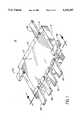
- FIG. 1shows a top view of a semiconductor die containing an electrical component on it surface.
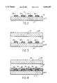
- FIG. 2shows a cross-sectional view of the die of FIG. 1 taken along section line 2--2.
- FIG. 3shows the die of FIG. 2 with a sealing cover in positioned in place in a layered relationship with the die.
- FIG. 4shows the die of FIG. 2 with the sealant applied to the die surface and the cover positioned in place in a layered relationship for sealing.
- FIG. 5shows an exploded view the die surface with the sealant applied to the cover.
- FIG. 6shows the die in a edge view with its layered cover pressed into place and forming a sealed package with the die and the sealant.
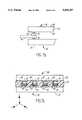
- FIG. 7ashows the die and a second die serving as a cover, with each containing a circuit, and with sealing material, in an exploded view.
- FIG. 7bshows an edge view of the dice of FIG. 7a assembled but without the sealing material, to show the positioning of the contacts of the dice.
- FIG. 7cshows an edge view of the dice and cover of FIG. 7a, assembled and environmentally sealed.
- FIG. 1shows in perspective, a semiconductor die 10 which may support or contain an electrical component such as an integrated circuit or a discrete semiconductor device, or any other kind of electrical component, whether active or passive, disposed on upper surface 15 of the semiconductor material 13.
- the surface 15may have a nitride or silica glass overcoat.
- the connection to the circuit on the semiconductor surfacewould be by a bonding pad 18 integral with the circuit and a conductive conduit (not shown), formed by plating for example, through the overcoat to a bump formed on the surface of the overcoat.
- the electrical componentmay be constructed using any technique including, without limitation, etching, deposition or printing.
- the electrical componentis contained within surface area 17 bounded by area boundary 16. It may be connected externally of the die 10 by means of leads 19a to 19g, it being understood that the number of leads is shown for illustrative purposes. The invention not being limited to the precise location of the leads or their number.
- a cross sectional view along edge 21 taken along line 2--2is shown in FIG. 2. The surface 15 is top most and with contacts 19a through 19d being shown arranged on surface 15. Also indicated by numeral 17 but not shown is the electrical operational area on surface 17.
- the area used for tile electrical componentis shown within the border 16, in FIG. 1.
- the operational areais a rectangle.
- the principles of the inventionmay be applied to any shape area on any surface of the component requiring an environmentally sealed cover.
- FIG. 3shows a cover 23 having an exterior (upper) surface 24 and an interior (lower) surface 22 positioned over a defined surface 15 of the semiconductor 13 and forming die 10.
- the cover 23is shown in alignment with the die 10.
- the cover 23is of the same area dimensions as the die 10 so when aligned with the die 10, the total surface area of the covered die in substantially that of the uncovered die 10.
- the cover materialmay be of the same material or material having selected compatible characteristics.
- the material selected for the covercould have the same coefficient of thermal expansion so distortions due to different rates of expansion under heating for the die 10 and the cover 23 are avoided. This expansion compatibility be augmented by alignment of crystalline structure in the die 10 and the matching cover 23.
- the lower surface of cover 23may have an electrical component formed on it with matching electrical contacts as would be known in the art. In this case, cover 23 would be a second die 20 and dice 10 and 20, when assembled would form an electrical system.
- a bead 27 of a sealant such as a purified epoxy adhesiveis placed around the boundary 16 and between the contacts 19.
- the adhesivefills the voids shown as 25 between adjacent contacts 19 where they extend along the periphery of the electrically operational area 17.
- the adhesive beadis placed outside the electrically operational area and on the contacts 19.
- the inventionis not limited to this placement but may include placing the adhesive inside the border 16 of the electrically operative area 17 or placement in any manner compatible with the structure and its circuitry.
- the die 10 of FIG. 1is shown with a bead of adhesive 27 applied about the periphery of the electrically operative area 17.
- the bead 27overlies the contacts 19.
- the cover of suitable material 23is shown placed opposite tile electrically operative surface area 17 and in a position to be applied to the die 10 as juxtaposed layer.
- the surface area cover 23is substantially coextensive with the defined area 17 to be covered and sealed on the die 10.
- the area enclosed by the epoxy adhesive 27includes surface area 15, enclosing the electrical operative surface 17.
- the defined areacan be expanded or reduced further to the limits of any area which requires environmental sealant.
- the sealant 27overlying the contacts 19 and filling the voids or spaces 25 between the contacts 19, forms a seal where it contacts the undersurface 22 of cover 23.
- the sealant 27initially may be placed on the matching interior surface 22 of the cover 23 as shown in the exploded view of FIG. 5.
- the sealmay be more advantageously viewed in the edge view of FIG. 6.
- the adhesive bead 27 in cooperation with cover 23 and the surface 15 of substrate 13seals and blocks any communication between the electrically operative surface 17 and the environment exterior to that surface 17.
- the view from any other side of substrate 13would be substantially similar.
- the principles of the inventionmay be applied to reducing the size of an electrical component to substantially to that of its electrical area.
- the covershould be the same material as the die 10 or a suitably compatible material, such as one having for example a matching coefficient of thermal expansion.
- FIG. 7ashows an exploded view of the die 10 with a cover 23 juxtaposed in a layered relationship over die 10.
- the cover 23, in this embodimentforms a second die 20, having constructed on its under surface 22 an electrical component.
- the connections from the electrical component in die 10may be more clearly seen in FIG. 7a as through the conductive bumps 31.
- the manner of constructing these bumps and the connection to the electrical component within defined surface area 17is well known in the art.
- the contacts 19are attached to the bumps 31 and the electrical component of die 10 may then be connected to other electrical components.
- the contacts 33 for the electrical component of die 20are constructed. This construction may be better viewed in FIG. 7b. In the view of FIG.
- the bumps 31 on dice 10 and 20are shown connected to their respective contacts 19 and 33.
- the contacts 33are shown for the preferred embodiment, it being understood the shape of the contacts can be varied to meet the physical needs of the specific application.
- contact between the die 10 and 20may be made directly by the direct connection of contacts or by any other suitable method, including reflow of solder or aluminum.
- the sealant 27may be placed between the contacts 33 or 19.
- sealant 27is shown between contacts 19a and 19b, or between contacts 33a and 33b.
- the electrical components of die 10 and 20are designed to cooperate with each other to form an electrical system.
- designated contacts of die 10will be arranged to be placed to contact respective matching contacts of die 20 to permit the cooperative use of the circuits on the two dice.
- the matching contactsmay be respective I/O ports for passing the signals required for interoperation of the dice 10 and 20 circuits.
- the contacts 19are shaped to provide electrical contacts as required to the environment exterior to the sealed space formed by die 10 and die 20, the contacts 19 and 33 and the sealant.
- FIG. 7bshows the die 20 placed over die for sealing and electrical connection. In this edge view, the placement of the sealant is omitted for clarity.
- the completed layered composite or sandwichis shown in edge view in FIG. 7c.
- the interior of the sandwich formed by die 10 and die 20is sealed from the environment by the sealant 27 in cooperation with the contacts 19 and 33.
- the sealantmay be applied on a strip shown as strip 35 in FIG. 7a.
- the stripmay contain conductive adhesive 37 for bonding with the contacts 19 and 33 and sealing in the proximity of these contacts. In between the conductive adhesive 37 may be placed non-conductive sealant which seals the interior of the layered composite or sandwich formed by die 10 and die 20 and insulated the contacts 19 and 33.
- a sealant which conducts only in the Z axis directionmay be used, according to the principles of the invention, to seal the interior of the space between die 10 and die 20. As this material conducts only in the direction between the dice, short circuits are avoided and the required contacts between matching terminals of the dice are made.
- the electrical components on die 10 and die 20 when assembled into a layered compositemay form a system or subsystem of a larger system.
- a system employing electrical components incapable of being assembled on a single integrated circuit or on a single semiconductor materialmay be assembled without exterior packaging and with a size limited to the surface area of each of the dice.
- circuits using different voltage levelssuch a power handler and controller may be so assembled.
- Other examplesare digital and analogue components, high frequency and low frequency components, reference generators and frequency synthesizers, discrete power transistors and associated control circuits.
- a thermally conductive sheet 41may be placed between the dice to promote the transfer of heat, to the bottom die 10 for example and out of the composite and the system. Additionally, multilayers may be added, increasing the complexity of the systems without adding to the surface area.
Landscapes
- Engineering & Computer Science (AREA)
- Physics & Mathematics (AREA)
- Condensed Matter Physics & Semiconductors (AREA)
- General Physics & Mathematics (AREA)
- Computer Hardware Design (AREA)
- Microelectronics & Electronic Packaging (AREA)
- Power Engineering (AREA)
- Manufacturing & Machinery (AREA)
- Structures Or Materials For Encapsulating Or Coating Semiconductor Devices Or Solid State Devices (AREA)
Abstract
Description
Claims (2)
Priority Applications (1)
| Application Number | Priority Date | Filing Date | Title |
|---|---|---|---|
| US07/831,252US5434357A (en) | 1991-12-23 | 1991-12-23 | Reduced semiconductor size package |
Applications Claiming Priority (1)
| Application Number | Priority Date | Filing Date | Title |
|---|---|---|---|
| US07/831,252US5434357A (en) | 1991-12-23 | 1991-12-23 | Reduced semiconductor size package |
Publications (1)
| Publication Number | Publication Date |
|---|---|
| US5434357Atrue US5434357A (en) | 1995-07-18 |
Family
ID=25258664
Family Applications (1)
| Application Number | Title | Priority Date | Filing Date |
|---|---|---|---|
| US07/831,252Expired - LifetimeUS5434357A (en) | 1991-12-23 | 1991-12-23 | Reduced semiconductor size package |
Country Status (1)
| Country | Link |
|---|---|
| US (1) | US5434357A (en) |
Cited By (22)
| Publication number | Priority date | Publication date | Assignee | Title |
|---|---|---|---|---|
| US5773323A (en)* | 1995-04-27 | 1998-06-30 | Lg Semicon Co., Ltd. | Package for solid state image sensing device and method for manufacturing thereof |
| US6040625A (en)* | 1997-09-25 | 2000-03-21 | I/O Sensors, Inc. | Sensor package arrangement |
| US6097087A (en)* | 1997-10-31 | 2000-08-01 | Micron Technology, Inc. | Semiconductor package including flex circuit, interconnects and dense array external contacts |
| USD466873S1 (en) | 2001-10-31 | 2002-12-10 | Siliconix Incorporated | Semiconductor chip package |
| US6499215B1 (en) | 2000-06-29 | 2002-12-31 | International Business Machines Corporation | Processing of circuit boards with protective, adhesive-less covers on area array bonding sites |
| USD472528S1 (en) | 2001-10-31 | 2003-04-01 | Siliconix Incorporated | Semiconductor chip package |
| US6576993B2 (en)* | 1999-06-18 | 2003-06-10 | Micron Technology, Inc. | Packages formed by attaching a semiconductor chip to a leadframe with a footprint of about the same size as the chip |
| USD489338S1 (en) | 2003-07-28 | 2004-05-04 | Semiconductor Components Industries, L.L.C. | Packaged semiconductor device |
| US6740960B1 (en) | 1997-10-31 | 2004-05-25 | Micron Technology, Inc. | Semiconductor package including flex circuit, interconnects and dense array external contacts |
| US20050250251A1 (en)* | 2000-08-23 | 2005-11-10 | Corisis David J | Method and apparatus for decoupling conductive portions of a microelectronic device package |
| USD731491S1 (en)* | 2014-02-07 | 2015-06-09 | NimbeLink L.L.C. | Embedded cellular modem |
| US9497570B2 (en) | 2014-02-06 | 2016-11-15 | Nimbelink Corp. | Embedded wireless modem |
| USD902877S1 (en)* | 2018-06-12 | 2020-11-24 | Rohm Co., Ltd. | Packaged semiconductor module |
| USD969762S1 (en)* | 2020-04-06 | 2022-11-15 | Wolfspeed, Inc. | Power semiconductor package |
| USD978809S1 (en)* | 2018-04-13 | 2023-02-21 | Rohm Co., Ltd. | Semiconductor module |
| USD1009819S1 (en)* | 2021-10-13 | 2024-01-02 | Rohm Co., Ltd. | Semiconductor device |
| USD1009818S1 (en)* | 2021-10-13 | 2024-01-02 | Rohm Co., Ltd. | Semiconductor device |
| USD1037187S1 (en)* | 2022-05-12 | 2024-07-30 | Alpha And Omega Semiconductor International Lp | Power semiconductor module |
| USD1042376S1 (en)* | 2022-02-25 | 2024-09-17 | Rohm Co., Ltd. | Semiconductor module |
| USD1042375S1 (en)* | 2022-05-12 | 2024-09-17 | Alpha And Omega Semiconductor International Lp | Power semiconductor module |
| USD1095474S1 (en)* | 2022-12-02 | 2025-09-30 | Semiconductor Components Industries, Llc | Power module package |
| USD1098055S1 (en)* | 2022-12-02 | 2025-10-14 | Semiconductor Components Industries, Llc | Power module package |
Citations (9)
| Publication number | Priority date | Publication date | Assignee | Title |
|---|---|---|---|---|
| US3310711A (en)* | 1962-03-23 | 1967-03-21 | Solid State Products Inc | Vertically and horizontally integrated microcircuitry |
| US3922705A (en)* | 1973-06-04 | 1975-11-25 | Gen Electric | Dielectrically isolated integral silicon diaphram or other semiconductor product |
| US4322737A (en)* | 1979-11-20 | 1982-03-30 | Intel Corporation | Integrated circuit micropackaging |
| US4970577A (en)* | 1988-04-12 | 1990-11-13 | Hitachi, Ltd. | Semiconductor chip module |
| US5013871A (en)* | 1988-02-10 | 1991-05-07 | Olin Corporation | Kit for the assembly of a metal electronic package |
| US5023398A (en)* | 1988-10-05 | 1991-06-11 | Olin Corporation | Aluminum alloy semiconductor packages |
| US5025114A (en)* | 1989-10-30 | 1991-06-18 | Olin Corporation | Multi-layer lead frames for integrated circuit packages |
| US5086018A (en)* | 1991-05-02 | 1992-02-04 | International Business Machines Corporation | Method of making a planarized thin film covered wire bonded semiconductor package |
| US5107074A (en)* | 1989-01-30 | 1992-04-21 | Ixys Corporation | Multi-lead hermetic power package with high packing density |
- 1991
- 1991-12-23USUS07/831,252patent/US5434357A/ennot_activeExpired - Lifetime
Patent Citations (9)
| Publication number | Priority date | Publication date | Assignee | Title |
|---|---|---|---|---|
| US3310711A (en)* | 1962-03-23 | 1967-03-21 | Solid State Products Inc | Vertically and horizontally integrated microcircuitry |
| US3922705A (en)* | 1973-06-04 | 1975-11-25 | Gen Electric | Dielectrically isolated integral silicon diaphram or other semiconductor product |
| US4322737A (en)* | 1979-11-20 | 1982-03-30 | Intel Corporation | Integrated circuit micropackaging |
| US5013871A (en)* | 1988-02-10 | 1991-05-07 | Olin Corporation | Kit for the assembly of a metal electronic package |
| US4970577A (en)* | 1988-04-12 | 1990-11-13 | Hitachi, Ltd. | Semiconductor chip module |
| US5023398A (en)* | 1988-10-05 | 1991-06-11 | Olin Corporation | Aluminum alloy semiconductor packages |
| US5107074A (en)* | 1989-01-30 | 1992-04-21 | Ixys Corporation | Multi-lead hermetic power package with high packing density |
| US5025114A (en)* | 1989-10-30 | 1991-06-18 | Olin Corporation | Multi-layer lead frames for integrated circuit packages |
| US5086018A (en)* | 1991-05-02 | 1992-02-04 | International Business Machines Corporation | Method of making a planarized thin film covered wire bonded semiconductor package |
Cited By (35)
| Publication number | Priority date | Publication date | Assignee | Title |
|---|---|---|---|---|
| US5773323A (en)* | 1995-04-27 | 1998-06-30 | Lg Semicon Co., Ltd. | Package for solid state image sensing device and method for manufacturing thereof |
| US6040625A (en)* | 1997-09-25 | 2000-03-21 | I/O Sensors, Inc. | Sensor package arrangement |
| US6740960B1 (en) | 1997-10-31 | 2004-05-25 | Micron Technology, Inc. | Semiconductor package including flex circuit, interconnects and dense array external contacts |
| US6097087A (en)* | 1997-10-31 | 2000-08-01 | Micron Technology, Inc. | Semiconductor package including flex circuit, interconnects and dense array external contacts |
| US6368896B2 (en) | 1997-10-31 | 2002-04-09 | Micron Technology, Inc. | Method of wafer level chip scale packaging |
| US6465877B1 (en) | 1997-10-31 | 2002-10-15 | Micron Technology, Inc. | Semiconductor package including flex circuit, interconnects and dense array external contacts |
| US6975037B2 (en) | 1997-10-31 | 2005-12-13 | Micron Technology, Inc. | Semiconductor package having flex circuit with external contacts |
| US20050156297A1 (en)* | 1997-10-31 | 2005-07-21 | Farnworth Warren M. | Semiconductor package including flex circuit, interconnects and dense array external contacts |
| US6911355B2 (en) | 1997-10-31 | 2005-06-28 | Micron Technology, Inc. | Semiconductor package having flex circuit with external contacts |
| US20040227218A1 (en)* | 1997-10-31 | 2004-11-18 | Farnworth Warren M. | Semiconductor package having flex circuit with external contacts |
| US20040140545A1 (en)* | 1997-10-31 | 2004-07-22 | Farnworth Warren M. | Method for fabricating semiconductor package having flex circuit, interconnects, and dense array external contacts |
| US6576993B2 (en)* | 1999-06-18 | 2003-06-10 | Micron Technology, Inc. | Packages formed by attaching a semiconductor chip to a leadframe with a footprint of about the same size as the chip |
| US6693349B2 (en) | 1999-06-18 | 2004-02-17 | Micron Technology, Inc. | Semiconductor chip package having a leadframe with a footprint of about the same size as the chip |
| US6624006B2 (en)* | 1999-06-18 | 2003-09-23 | Micron Technology, Inc. | Methods of attaching a semiconductor chip to a leadframe with a footprint of about the same size as the chip |
| US6499215B1 (en) | 2000-06-29 | 2002-12-31 | International Business Machines Corporation | Processing of circuit boards with protective, adhesive-less covers on area array bonding sites |
| US6700068B2 (en)* | 2000-06-29 | 2004-03-02 | International Business Machines Corporation | Adhesive-less cover on area array bonding site of circuit board |
| US7378723B2 (en) | 2000-08-23 | 2008-05-27 | Micron Technology, Inc. | Method and apparatus for decoupling conductive portions of a microelectronic device package |
| US20050250251A1 (en)* | 2000-08-23 | 2005-11-10 | Corisis David J | Method and apparatus for decoupling conductive portions of a microelectronic device package |
| US7183138B2 (en) | 2000-08-23 | 2007-02-27 | Micron Technology, Inc. | Method and apparatus for decoupling conductive portions of a microelectronic device package |
| US20070052087A1 (en)* | 2000-08-23 | 2007-03-08 | Micron Technology, Inc. | Method and apparatus for decoupling conductive portions of a microelectronic device package |
| USD466873S1 (en) | 2001-10-31 | 2002-12-10 | Siliconix Incorporated | Semiconductor chip package |
| USD472528S1 (en) | 2001-10-31 | 2003-04-01 | Siliconix Incorporated | Semiconductor chip package |
| USD489338S1 (en) | 2003-07-28 | 2004-05-04 | Semiconductor Components Industries, L.L.C. | Packaged semiconductor device |
| US9497570B2 (en) | 2014-02-06 | 2016-11-15 | Nimbelink Corp. | Embedded wireless modem |
| USD731491S1 (en)* | 2014-02-07 | 2015-06-09 | NimbeLink L.L.C. | Embedded cellular modem |
| USD978809S1 (en)* | 2018-04-13 | 2023-02-21 | Rohm Co., Ltd. | Semiconductor module |
| USD902877S1 (en)* | 2018-06-12 | 2020-11-24 | Rohm Co., Ltd. | Packaged semiconductor module |
| USD969762S1 (en)* | 2020-04-06 | 2022-11-15 | Wolfspeed, Inc. | Power semiconductor package |
| USD1009819S1 (en)* | 2021-10-13 | 2024-01-02 | Rohm Co., Ltd. | Semiconductor device |
| USD1009818S1 (en)* | 2021-10-13 | 2024-01-02 | Rohm Co., Ltd. | Semiconductor device |
| USD1042376S1 (en)* | 2022-02-25 | 2024-09-17 | Rohm Co., Ltd. | Semiconductor module |
| USD1037187S1 (en)* | 2022-05-12 | 2024-07-30 | Alpha And Omega Semiconductor International Lp | Power semiconductor module |
| USD1042375S1 (en)* | 2022-05-12 | 2024-09-17 | Alpha And Omega Semiconductor International Lp | Power semiconductor module |
| USD1095474S1 (en)* | 2022-12-02 | 2025-09-30 | Semiconductor Components Industries, Llc | Power module package |
| USD1098055S1 (en)* | 2022-12-02 | 2025-10-14 | Semiconductor Components Industries, Llc | Power module package |
Similar Documents
| Publication | Publication Date | Title |
|---|---|---|
| US5434357A (en) | Reduced semiconductor size package | |
| US5899705A (en) | Stacked leads-over chip multi-chip module | |
| US4974057A (en) | Semiconductor device package with circuit board and resin | |
| US5811879A (en) | Stacked leads-over-chip multi-chip module | |
| US5578525A (en) | Semiconductor device and a fabrication process thereof | |
| US5448106A (en) | Thin semiconductor integrated circuit device assembly | |
| US5600181A (en) | Hermetically sealed high density multi-chip package | |
| KR100281830B1 (en) | Thermally Enhanced Flip Chip Packages and Manufacturing Method | |
| US4423468A (en) | Dual electronic component assembly | |
| US6628526B1 (en) | Electronic device manufacturing method, electronic device and resin filling method | |
| US20100140787A1 (en) | Semiconductor device, semiconductor package for use therein, and manufacturing method thereof | |
| EP1189273A2 (en) | Semiconductor device and production process | |
| US4423435A (en) | Assembly of an electronic device on an insulative substrate | |
| JPS63211663A (en) | circuit board | |
| JPH0319703B2 (en) | ||
| US20060022325A1 (en) | Cap wafer, semiconductor package, and fabricating method thereof | |
| US20040217451A1 (en) | Semiconductor packaging structure | |
| KR100387451B1 (en) | Semiconductor device and method of manufacturing the same | |
| US5679979A (en) | Surface mount package with heat transfer feature | |
| JP2975782B2 (en) | Hybrid integrated circuit device and case material used therefor | |
| JP3045940B2 (en) | Semiconductor device and manufacturing method thereof | |
| JPS63107126A (en) | Semiconductor device | |
| JPS60160146A (en) | Semiconductor device | |
| JPH1012810A (en) | Semiconductor device | |
| JPH0810746B2 (en) | Memory module |
Legal Events
| Date | Code | Title | Description |
|---|---|---|---|
| STCF | Information on status: patent grant | Free format text:PATENTED CASE | |
| AS | Assignment | Owner name:HARRIS CORPORATION, FLORIDA Free format text:ASSIGNMENT OF ASSIGNORS INTEREST;ASSIGNORS:BELCHER, DONALD K.;ADKINS, CALVIN I.;REEL/FRAME:008744/0847 Effective date:19920309 | |
| FEPP | Fee payment procedure | Free format text:PAYOR NUMBER ASSIGNED (ORIGINAL EVENT CODE: ASPN); ENTITY STATUS OF PATENT OWNER: LARGE ENTITY | |
| FPAY | Fee payment | Year of fee payment:4 | |
| AS | Assignment | Owner name:INTERSIL CORPORATION, FLORIDA Free format text:ASSIGNMENT OF ASSIGNORS INTEREST;ASSIGNOR:HARRIS CORPORATION;REEL/FRAME:010247/0043 Effective date:19990813 | |
| AS | Assignment | Owner name:CREDIT SUISSE FIRST BOSTON, AS COLLATERAL AGENT, N Free format text:SECURITY INTEREST;ASSIGNOR:INTERSIL CORPORATION;REEL/FRAME:010351/0410 Effective date:19990813 | |
| FPAY | Fee payment | Year of fee payment:8 | |
| FPAY | Fee payment | Year of fee payment:12 | |
| AS | Assignment | Owner name:MORGAN STANLEY & CO. INCORPORATED,NEW YORK Free format text:SECURITY AGREEMENT;ASSIGNORS:INTERSIL CORPORATION;TECHWELL, INC.;INTERSIL COMMUNICATIONS, INC.;AND OTHERS;REEL/FRAME:024390/0608 Effective date:20100427 | |
| AS | Assignment | Owner name:INTERSIL CORPORATION,FLORIDA Free format text:RELEASE BY SECURED PARTY;ASSIGNOR:CREDIT SUISSE FIRST BOSTON;REEL/FRAME:024445/0049 Effective date:20030306 |