US5432461A - Method of testing active matrix liquid crystal display substrates - Google Patents
Method of testing active matrix liquid crystal display substratesDownload PDFInfo
- Publication number
- US5432461A US5432461AUS07/722,963US72296391AUS5432461AUS 5432461 AUS5432461 AUS 5432461AUS 72296391 AUS72296391 AUS 72296391AUS 5432461 AUS5432461 AUS 5432461A
- Authority
- US
- United States
- Prior art keywords
- liquid crystal
- crystal display
- active matrix
- electro
- matrix liquid
- Prior art date
- Legal status (The legal status is an assumption and is not a legal conclusion. Google has not performed a legal analysis and makes no representation as to the accuracy of the status listed.)
- Expired - Lifetime
Links
Images


Classifications
- G—PHYSICS
- G09—EDUCATION; CRYPTOGRAPHY; DISPLAY; ADVERTISING; SEALS
- G09G—ARRANGEMENTS OR CIRCUITS FOR CONTROL OF INDICATING DEVICES USING STATIC MEANS TO PRESENT VARIABLE INFORMATION
- G09G3/00—Control arrangements or circuits, of interest only in connection with visual indicators other than cathode-ray tubes
- G09G3/006—Electronic inspection or testing of displays and display drivers, e.g. of LED or LCD displays
- G—PHYSICS
- G01—MEASURING; TESTING
- G01R—MEASURING ELECTRIC VARIABLES; MEASURING MAGNETIC VARIABLES
- G01R31/00—Arrangements for testing electric properties; Arrangements for locating electric faults; Arrangements for electrical testing characterised by what is being tested not provided for elsewhere
- G01R31/28—Testing of electronic circuits, e.g. by signal tracer
- G01R31/302—Contactless testing
- G01R31/308—Contactless testing using non-ionising electromagnetic radiation, e.g. optical radiation
- G01R31/311—Contactless testing using non-ionising electromagnetic radiation, e.g. optical radiation of integrated circuits
- G—PHYSICS
- G01—MEASURING; TESTING
- G01N—INVESTIGATING OR ANALYSING MATERIALS BY DETERMINING THEIR CHEMICAL OR PHYSICAL PROPERTIES
- G01N21/00—Investigating or analysing materials by the use of optical means, i.e. using sub-millimetre waves, infrared, visible or ultraviolet light
- G01N21/84—Systems specially adapted for particular applications
- G01N21/88—Investigating the presence of flaws or contamination
- G01N21/95—Investigating the presence of flaws or contamination characterised by the material or shape of the object to be examined
- G01N2021/9513—Liquid crystal panels
- G—PHYSICS
- G02—OPTICS
- G02F—OPTICAL DEVICES OR ARRANGEMENTS FOR THE CONTROL OF LIGHT BY MODIFICATION OF THE OPTICAL PROPERTIES OF THE MEDIA OF THE ELEMENTS INVOLVED THEREIN; NON-LINEAR OPTICS; FREQUENCY-CHANGING OF LIGHT; OPTICAL LOGIC ELEMENTS; OPTICAL ANALOGUE/DIGITAL CONVERTERS
- G02F1/00—Devices or arrangements for the control of the intensity, colour, phase, polarisation or direction of light arriving from an independent light source, e.g. switching, gating or modulating; Non-linear optics
- G02F1/01—Devices or arrangements for the control of the intensity, colour, phase, polarisation or direction of light arriving from an independent light source, e.g. switching, gating or modulating; Non-linear optics for the control of the intensity, phase, polarisation or colour
- G02F1/13—Devices or arrangements for the control of the intensity, colour, phase, polarisation or direction of light arriving from an independent light source, e.g. switching, gating or modulating; Non-linear optics for the control of the intensity, phase, polarisation or colour based on liquid crystals, e.g. single liquid crystal display cells
- G02F1/1306—Details
- G02F1/1309—Repairing; Testing
- Y—GENERAL TAGGING OF NEW TECHNOLOGICAL DEVELOPMENTS; GENERAL TAGGING OF CROSS-SECTIONAL TECHNOLOGIES SPANNING OVER SEVERAL SECTIONS OF THE IPC; TECHNICAL SUBJECTS COVERED BY FORMER USPC CROSS-REFERENCE ART COLLECTIONS [XRACs] AND DIGESTS
- Y10—TECHNICAL SUBJECTS COVERED BY FORMER USPC
- Y10S—TECHNICAL SUBJECTS COVERED BY FORMER USPC CROSS-REFERENCE ART COLLECTIONS [XRACs] AND DIGESTS
- Y10S345/00—Computer graphics processing and selective visual display systems
- Y10S345/904—Display with fail/safe testing feature
Definitions
- This inventionrelates to a testing method for the detection of defects produced in active matrix liquid crystal display substrates used as liquid crystal display panels, or the like.
- Active-matrix type liquid crystal display panelsare formed using active-matrix liquid crystal display substrates which comprise pixel electrodes for each pixel element, arranged in a matrix pattern, gate lines which are common to all pixel electrodes, source lines, and thin film transistors.
- active-matrix liquid crystal display substrateswhich comprise pixel electrodes for each pixel element, arranged in a matrix pattern, gate lines which are common to all pixel electrodes, source lines, and thin film transistors.
- liquid crystal televisionswhich are presently produced using this technique, there are many units which reach a pixel count of 250,000-500,000. Some have reached the market having a pixel count of over 1,000,000.
- Formation of the pixels, and the numerous lines thereto corresponding, on a substrateinvolve various formation processes which are carried out in a clean room.
- the clean roomis controlled so that there is very little dust contained therein.
- the pixels or the line widthis extremely small, the presence of a small amount of microdust in the manufacturing atmosphere is directly linked to open-circuit or short-circuit defects of the pixel electrodes, gate lines or source lines. Presently, up to ten such defects are permitted. It is common to classify products as defective if the number of defects exceeds ten.
- Present testinguses a probe to test active matrix liquid crystal display substrates when manufacturing is completed.
- the number of elements on the active matrix liquid crystal display substrateis very large, an excessive amount of time is required for testing, and this approach becomes impractical.
- the present inventionprovides a testing method for active-matrix liquid crystal display substrates having thin film transistors, a plurality of pixel electrodes, source lines, and gate lines formed on a substrate.
- a high resolution electro-optical elementin which the optical properties change when an electrical field is impressed across it, is placed above the active matrix liquid crystal display substrate and separated therefrom by an extremely small gap.
- a voltageis applied between the pixel electrodes on the active matrix liquid crystal display substrate and a transparent thin film electrode on the surface of the electro-optical element creating an electrical field across the electro-optical element.
- the present inventionuses polymer-dispersed liquid crystals as the electro-optical element and detects defects in the pixels by detecting changes in the light transmission rate of the polymer-dispersed liquid crystals.
- the present inventionmay also use Pockels crystals as the electro-optical element and detects defects in the pixels by detecting changes in the amount of polarization of reflected light.
- the present inventionirradiates the electro-optical element with light and receives the light reflected from the electro-optical element in a light detector, converts the amount of change in the reflected light to a corresponding voltage, and thus discerns the presence of defects in the pixels.
- the electro-optical elementWhen an electric field is impressed on the electro-optical element, its optical properties change.
- this electro-optical elementWhen this electro-optical element is placed above the active matrix liquid crystal display substrate and an electric voltage applied between the pixel electrodes on the active matrix liquid crystal display substrate and transparent thin film electrodes on the electro-optical device, the optical properties of the electro-optical element change based on the magnitude of the electric field generated by each pixel electrode.
- the polymer-dispersed liquid crystalhas an area in which the amount of light scattered is linearly proportional to the change in voltage. It is possible to take advantage of this linearity, and to relate the change in voltage as the change in the amount of light transmitted. It is preferable to apply a bias voltage up to this linear area.
- the qualities of polymer-dispersed liquid crystalsare especially suited to testing active matrix liquid crystal display substrates having extremely small lines or pixel electrodes. It is preferable to affix mylar, or the like, to the surface opposing the substrate of the polymer-dispersed liquid crystal as an insulating material so that the pixels on the active matrix liquid crystal display substrate are not destroyed.
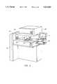
- FIG. 1is a block diagram showing an outline of the main parts of a test apparatus which is used in one embodiment of the present invention
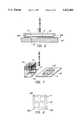
- FIG. 2(a)is a partially expanded view of the active matrix liquid crystal display substrate tested by the present invention
- FIGS. 2(b)-(f)are top views showing examples of shorting bars
- FIG. 2(g)is a block diagram showing a voltage source apparatus
- FIG. 3is a block diagram showing the testing apparatus
- FIG. 4is a block diagram of the interior test head of the testing apparatus
- FIG. 5is a more detailed drawing of the test head
- FIG. 6is a side view showing the positioning of the holder used in the test apparatus and the active matrix liquid crystal display substrate;
- FIG. 7is a diagram showing retrieval of the active matrix liquid crystal display substrate from substrate storage
- FIG. 8is a diagram of the active matrix liquid crystal display substrate
- FIG. 9is a flow chart illustrating test flow
- FIG. 10is a cross sectional diagram of the liquid crystal sheet across which an electric field is not being impressed.
- FIG. 11is a cross sectional diagram showing the liquid crystal sheet across which an electric field is being impressed
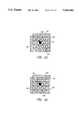
- FIGS. 12-17are expanded views to aid in explaining defective parts in the active matrix liquid crystal display substrate.
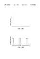
- FIGS. 18a, 18b, 19a, 19b, 20a and 20bare graphs to aid in explaining examples of the voltage which is applied during testing.
- the test apparatusis provided with a light source 1, and an electro-optical element 2 onto which the detection light is radiated by light source 1.
- a light detector 3receives light reflected from the electro-optical element 2.
- a monitor 4is connected to the light detector 3.
- An active matrix liquid crystal display substrate 5is disposed facing, and slightly spaced apart from the opposing surface of electro-optical element 2.
- Reference number 7indicates a voltage source which applies a fixed voltage between transparent thin film electrode 2a on the upper surface of electro-optical element 2 and active matrix liquid crystal display substrate 5.
- the voltage sourceis able to apply pulsed voltages separately to the source lines and gate lines, and can change the pulse voltage, pulse width, and period. Further details will be given hereinafter.
- Light source 1is a halogen lamp in one preferred embodiment. It is possible to use any type of laser light in place of the halogen lamp as light source 1.
- the electro-optical element 2is a polymer dispersed liquid crystal or Pockels crystal, or the like, the optical properties of which change when an electrical field is applied across it.
- the electro-optical element 2 shown in FIG. 1is a sheet form polymer dispersed liquid crystal in which a reflecting body 9, such as non-conductive reflecting film or the like formed on the bottom surface of liquid crystal sheet 8, and transparent thin film electrode 2a are attached to the upper surface of liquid crystal sheet 8.
- Liquid crystal sheet 8is filled with NCAP (Nematic Curvilinear Aligned Phase) material which has a transmission rate which changes according to the magnitude of the electrical field created across liquid crystal sheet 8.
- NCAPNatural Curvilinear Aligned Phase
- the liquid crystal which fills the interior of liquid crystal sheet 8is of a form in which a drop-shaped liquid crystal is dispersed in a high molecular weight substance, such as a polymer.
- the size of the ball-shaped droplets of the polymer which contains the resulting liquid crystalare controlled, and based on the magnitude of the electric field, a transparent state or a nontransparent state is caused to appear based on the agreement or disagreement of the index of refraction of the polymer and the liquid crystal.
- electro-optical element 2used in the present preferred embodiment has optical properties which change when an electric field is impressed across it, such as the transmission rate of light or the amount of polarization of the reflected light, then electro-optical element 2 is not limited to the above, but any such element may be used.
- a CCD camera or the likeis used as light detector 3.
- the active matrix liquid crystal display substrate 5 which is tested by the present methodis commonly known and is used in liquid crystal display panels. As shown in FIG. 2, a number of source lines for the transmission of data signals, and a number of gate lines for the transmission of scanning signals, are formed on a substrate 12. Pixel electrodes 13 are formed between the source lines and gate lines. Each pixel electrode 13 is connected to source lines 10 and gate lines 11 through switching elements (thin film transistors) 14.
- Reference number 15 shown in FIG. 2(a)indicates a shorting bar connecting source lines 10 and reference number 16 indicates a shorting bar connecting gate lines 11.
- Shorting bars 15 and 16are formed in the manufacturing process of active matrix liquid crystal display substrate 5. They are cut and removed manufacturing the liquid crystal display panel.
- Shorting bars 15 and 16prevent static electricity from causing deleterious effects on the thin film transistors, and assist in the present testing method, (if they are in one of the forms shown in FIGS. 2(b)-2(f)). If mounted drivers are used in place of the shorting bars, the testing method of the present invention can still be used. Detection of line defects on the source and gate lines in FIG. 2(b), as well as line defects on the source lines in FIG. 2(c), has been thought to be difficult without optical techniques. However, at the substrate stage, even point defects which have been difficult to detect, can be detected using the present invention.
- Voltage source 7is provided with a switch 7a.
- a voltage source part 7bis connected to the transparent thin film electrode 2a on the upper surface of electro-optical element 2, and to the shorting bars 15 and 16 on active matrix liquid crystal display substrate 5, and is able to apply voltage from the gate lines and the source lines on all pixel electrodes 13 on active matrix liquid crystal display substrate 5.
- the voltage source 7is able to apply pulsed voltages separately on source lines 10 and gate lines 11 and is able to freely change the pulse voltage, pulse width, and period.
- FIG. 2(g)The construction of the connection of the voltage source 7 is shown in FIG. 2(g).
- a shorting baris formed like that shown in FIG. 2(g)
- a voltage pulse within the range of ⁇ 15 V from voltage source 7makes contact with shorting bars 15 and 16 from two separate, independent terminals which are capable of current detection on the gate and source lines.
- Wiringis provided to transparent thin film electrode 2a on the upper surface of the electro-optical element from one terminal which is able to apply a fixed voltage with respect to the two terminals connected to shorting bars 15 and 16.
- reference number 20indicates a test bed.
- Reference number 21indicates a substrate storage part (cassette rack) disposed at the left side of test bed 20.
- Reference number 22indicates a test head, and reference number 23 indicates an operation board.
- a left to right guide rail 25is laid on the upper surface of test bed 20, in the central part thereof.
- Table 26runs along this guide rail 25 in the left and right directions.
- Mechanismsare installed on the bottom part of table 26 which move table 26 at right angles with respect to guide rail 25 so that table 26 is able to move in left, right, forward, and backward directions (that is, in the directions X and Y) above test bed 20 in a horizontal plane.
- a cassette 27(see FIG. 7), stores a plurality of active matrix liquid crystal display substrates 5. Active matrix liquid crystal display substrates 5 are successively retrieved from the open mouth part of cassette 27 from the upper part of this substrate storage part 21 and are set on top of table 26.
- FIG. 4An outline of the composition of the inner part of test head 22 is shown in FIG. 4 and detailed construction of the inner part is shown in FIG. 5.
- each optical device in FIG. 5can be freely changed by changing the setting position of the liquid crystal panel or the direction.
- FIG. 4 and FIG. 5an example is shown in which the panel has been arranged lengthwise.
- Light source 1 and light detector 3are provided in the inner part of testing head 22.
- Light source 1 and light detector 3each face a beam splitter 30.
- a lens 31 and a filter 31aprovide adjustment between the beam splitter 30 and light source 1.
- a lens 32provides for adjustment between beam splitter 30 and light detector 3.
- a holder 33 on which electro-optical element 2 is mountedis located on the left side of beam splitter 30 in FIG. 4. This holder 33 is capable of parallel movement in the left and right directions of FIG. 4 and FIG. 5 along support axles 34.
- a zoom lens 35is mounted at the forward part of light detector 3, making possible the highly efficient entry of flight reflected from electro-optical element 2 into light detector 3.
- Light emitted from light source 1is irradiated onto electro-optical element 2 through beam splitter 30. After being reflected from the light reflection body 9 of electro-optical element 2, the light passes back through beam splitter 30, lens 32 and zoom lens 35 and into light detector 3.
- reference number 40indicates a controller.
- this control part 40is an analog-to-digital (A/D) converter 41 which is electrically connected to light detector 3, an image processor 42, a drive circuit 43, and a CPU 44.
- a display 4is connected to image processor 42.
- Operation board 23is connected to CPU 44.
- Controller 40converts the intensity of the light received by light detector 3 to a corresponding voltage and displays this strength. Controller 40 also displays the number of defects in the active matrix liquid crystal display substrate 5 and their positions and types in monitor 4 in response to the corresponding voltage distribution. When the number of defects is displayed, the dimensions of each pixel are inputted, and masking is conducted based on the corresponding voltage distribution.
- a passage 27 for air or vacuumcommunicates the upper and lower sides of table 26, and is formed in table 26.
- a flexible pipe(not shown) is connected to the lower opening of passage 27 in such a way as not to obstruct the movement of table 26.
- This flexible pipeis connected to a vacuum. In this manner, an active matrix liquid crystal display substrate 5 is held on the upper surface of table 26 by vacuum adhesion through passage 27.
- active matrix liquid crystal display substrates 5are manufactured by the formation of source lines 10, gate lines 11, pixel electrodes 13, switching elements 14, shorting bar 15, and shorting bar 16 on a substrate 12 by mask formation, thin film formation, photo resist, exposing the photo resist, etching, washing, ion impregnation, or similar various processes.
- This production lineis shown as step S1 in FIG. 9.
- a plurality of rectangular areascomprising source lines 10, gate lines 11, pixel electrodes 13, switching elements 14, shorting bar 15, and shorting bar 16, are formed on one substrate 12.
- step 2the active matrix liquid crystal display substrates 5 are conveyed to substrate storage part 21 of the testing apparatus and are stored in a cassette.
- step 3the active matrix liquid crystal display substrates 5 stored in substrate storage part 21 are retrieved from substrate storage part 21 and are placed on table 26.
- step S4the active matrix liquid crystal display substrate 5 is affixed to the upper surface of table 26 by vacuum adhesion.
- step S5table 26 is moved along guide rail 25 (movement in the direction of the X-axis) to the area opposing scanning head 22.
- step 6table 26 is moved in a forward and backward direction for small distances, accurately positioning table 26 beneath scanning head 2.
- step S7holder 33 provided on scanning head 22 moves downward and electro-optical element 2 is positioned adjacent to active matrix liquid crystal display substrate 5. At this time, the positioning pivots 33a on the outer part of holder 33 are attached (by compression) to fixed positions on active matrix liquid crystal display substrate 5.
- Positioningis such that, as shown in FIG. 8, a plurality (in this example 4) of areas are formed on a rectangular substrate 12. Positioning pivots 33a of holder 33 make contact at fixed positions at the four corners of substrate 12, and active matrix liquid crystal display substrate 5 and electro-optical element 2 are aligned in parallel.
- step S8an electrode of voltage source 7 makes contact with shorting bars 15 and 16 of the active matrix liquid crystal display substrate 5.
- step S81the voltage value is slowly raised so as to become positive with respect to the source side and the gate side, and the current between source lines 10 and gate lines 11 is monitored for leakage. If current leakage is detected, a determination is made that a short (called a cross short) has occurred between source lines 10 and gate lines 11. If there is no leaking current, step S9 is proceeded to.
- active matrix liquid crystal display substrate 5 in which a cross short has been detectedin step S81 it is determined whether the active matrix liquid crystal display substrate will be repaired by a repair apparatus or be rejected and disposed of.
- step S9a bias voltage is applied between the electrode on the upper surface of the electro-optical element and the gate side and the source side in step 8.
- This bias voltageis a voltage of maximally +15 V with respect to a standard voltage (for example, a grounding level) and is applied in an appropriate mode, and defect testing is thus conducted. In this manner, an electric field is generated between transparent thin film electrodes 2a on the upper surface of the electro-optical element and the pixel electrodes on active matrix liquid crystal display substrate 5.
- liquid crystal sheet 8When a liquid crystal sheet 8 is used as electro-optical element 2, when an electric field is not being applied, as shown in FIG. 10, the (ball form) liquid crystal molecules face in disordered directions, scatter the light, and do not permit the transmission of light. When an electric field is impressed as shown in FIG. 11, the liquid crystal molecules (in ball form) all face in a single direction and permit the transmission of light. There is an area in which the transparent electrodes change in linear proportion to voltage changes with respect to the polymer-dispersed liquid crystals. Using this linearity, it is possible to determine the change in voltage as a change in the amount of light transmitted. A bias voltage is applied between pixel electrodes 13 and transparent thin film electrodes 2a on electro-optical element 2 correspond to this linear region.
- electro-optical element 2If a liquid crystal sheet 8 is used, by applying a voltage between the pixel electrodes 13 and the transparent thin film electrodes 2a of electro-optical element 2, an electric field is generated, and electro-optical element 2 has an amount of light transmitted which changes in response to changes in the electric field generated by each pixel electrode 13.
- step S9light is irradiated from light source 1 onto electro-optical element 2. This light passes through electro-optical element 2 and is reflected by light reflecting body 9. The strength of the light which again passes through electro-optical element 2 is measured by light detector 3.
- step S10the light received by light detector 3 is calculated in controller 40, and a corresponding voltage is calculated. Provided the value of this corresponding voltage can be specified, the corresponding voltage generated by each pixel is checked based on a threshold value which is determined.
- step S11based on the brightness of the picture or the value of the corresponding voltage, a determination judgement is made as to whether the pixels are defective or not. In order to determine whether an active matrix liquid crystal display substrate 5 is to be accepted or not, standards are used. If a value indicating how many defects are allowed, in a liquid crystal display element with 1,000,000 pixels is decided in advance, a user can determine whether an active matrix liquid crystal display substrate 5 is acceptable based on data of the processing screen.
- step S12If the number of defects in an active matrix liquid crystal display substrate 5 is within an acceptable range, the active matrix liquid crystal display substrate 5 is conveyed to the next process in step S12.
- repairable unitsare sent to a repair station in step S13, or in step S14 are sent to a cutting apparatus, or a deposit apparatus and repaired. After repair, it is possible to return the units to the manufacturing line in step S12.
- step S11Units which have been determined to be difficult to repair in step S11 are rejected and disposed of in step S15.
- the voltage applied with respect to the gate and source linesis 0 v. in the initial condition.
- the brightness of the pixel electrodes 13 of the active matrix liquid crystal display substrate 5were shown for ease of understanding. In reality, the parts of the electro-optical element 2 corresponding to pixel electrodes 13 are observed as a brightness distribution. By referring this brightness to a one-pixel dimensional pitch in controller 40, a technique for discriminating the brightness of the pixel elements is obtained.
- the voltage applied on the gate and source linesis 0 v., as the initial condition.
- one pixel electrode 13becomes dark at a location shown by the blackened part in FIG. 13, while the other, normal pixel electrodes 13 do not change as shown by the slanted lines.
- the present inventionrecreates a test which is close to the conventional final test before forming active matrix liquid crystal display substrates 5 into liquid crystal panels.
- the present inventionis capable of detecting defects prior to completing the manufacture of liquid crystal panels relatively easily, and is useful in increasing the rate of acceptable products in line.
- the testing method of the present inventionWhen the testing method of the present invention is employed, it is possible to test for short-circuited electrodes, as shown in FIGS. 12-17. It is possible to move the substrates in a fashion in which protection from static electricity is maintained, especially for processes in which static electricity is more likely to be generated, such as assembly of liquid crystal panels, or the like.
- Various configurationsincluding units which have an IC driver mounted in place of a short circuit electrode, or units which have a drive circuit mounted, or substrates having a drive circuit, or substrates having no short circuit electrode, can also be tested.
- the present inventionmay be used on any substrate configuration.
- the electro-optical elementcan be used without any restriction based on the dimensions of the pixel electrodes on the active matrix liquid crystal display substrate (which is the object of testing) such that it has a broad range of applications, is highly reliable, and the costs thereof are relatively low.
- Light reflected from the electro-optical element 2is converted to a corresponding voltage and defects are determined based on this corresponding voltage, so that it is possible to quickly conduct tests in a short time.
- the inventorsconducted tests on a 10-inch active matrix liquid crystal display substrate using a liquid crystal sheet as the electro-optical element and a test apparatus which was actually constructed such that the resolution of the liquid crystal sheet was 50 ⁇ m. It was possible to conduct testing, including handling (including the machine controlled speed) of active matrix liquid crystal display substrates 5 at a rate of more than 12 per hour.
- an electro-optical elementis disposed over an active matrix liquid crystal display substrate which is to be tested.
- An electric voltageis then applied between the pixel electrodes on the active matrix liquid crystal display substrate and the transparent thin film electrodes on the upper surface of the electro-optical element.
- the optical properties of the electro-optical elementcause a change in the light which is transmitted through the electro-optical element. These changes are detected by a light detector.
- the detection of defects in an active matrix liquid crystal display substrateis thus carried out, so that by monitoring the output of the light detector, defects in the active matrix liquid crystal display substrate can be detected as a group electrically, and reliable and rapid testing can be accomplished.
Landscapes
- Engineering & Computer Science (AREA)
- Physics & Mathematics (AREA)
- General Physics & Mathematics (AREA)
- Computer Hardware Design (AREA)
- Liquid Crystal (AREA)
- Microelectronics & Electronic Packaging (AREA)
- Health & Medical Sciences (AREA)
- Computer Vision & Pattern Recognition (AREA)
- Electromagnetism (AREA)
- Toxicology (AREA)
- General Engineering & Computer Science (AREA)
- Theoretical Computer Science (AREA)
- Testing Of Short-Circuits, Discontinuities, Leakage, Or Incorrect Line Connections (AREA)
- Testing Electric Properties And Detecting Electric Faults (AREA)
- Tests Of Electronic Circuits (AREA)
Abstract
Description
Claims (7)
Priority Applications (2)
| Application Number | Priority Date | Filing Date | Title |
|---|---|---|---|
| US07/722,963US5432461A (en) | 1991-06-28 | 1991-06-28 | Method of testing active matrix liquid crystal display substrates |
| JP19278592AJP3275103B2 (en) | 1991-06-28 | 1992-06-29 | Inspection method for active matrix liquid crystal display substrate |
Applications Claiming Priority (1)
| Application Number | Priority Date | Filing Date | Title |
|---|---|---|---|
| US07/722,963US5432461A (en) | 1991-06-28 | 1991-06-28 | Method of testing active matrix liquid crystal display substrates |
Publications (1)
| Publication Number | Publication Date |
|---|---|
| US5432461Atrue US5432461A (en) | 1995-07-11 |
Family
ID=24904207
Family Applications (1)
| Application Number | Title | Priority Date | Filing Date |
|---|---|---|---|
| US07/722,963Expired - LifetimeUS5432461A (en) | 1991-06-28 | 1991-06-28 | Method of testing active matrix liquid crystal display substrates |
Country Status (2)
| Country | Link |
|---|---|
| US (1) | US5432461A (en) |
| JP (1) | JP3275103B2 (en) |
Cited By (58)
| Publication number | Priority date | Publication date | Assignee | Title |
|---|---|---|---|---|
| US5539326A (en)* | 1994-06-07 | 1996-07-23 | Tohken Industries Co., Ltd. | Method for testing the wiring or state of a liquid crystal display and thin film transistor |
| US5608558A (en)* | 1994-04-26 | 1997-03-04 | Sharp Kabushiki Kaisha | Defect detection method and apparatus for active matrix substrate or active matrix liquid crystal panel and defect repairing method thereof |
| US5694053A (en)* | 1995-06-07 | 1997-12-02 | Xerox Corporation | Display matrix tester |
| US5726673A (en)* | 1992-11-11 | 1998-03-10 | Kabushiki Kaisha Komatsu Seisakusho | Liquid crystal display for laser marker |
| US5751262A (en)* | 1995-01-24 | 1998-05-12 | Micron Display Technology, Inc. | Method and apparatus for testing emissive cathodes |
| US5754305A (en)* | 1996-12-03 | 1998-05-19 | Eastman Kodak Company | Method and apparatus for correcting light non-uniformity in an LCD photographic printer |
| US5781230A (en)* | 1994-12-19 | 1998-07-14 | Lucent Technologies, Inc. | Method and apparatus for illuminating translucent and semi-transparent material |
| US5793221A (en)* | 1995-05-19 | 1998-08-11 | Advantest Corp. | LCD panel test apparatus having means for correcting data difference among test apparatuses |
| US5801764A (en)* | 1994-07-11 | 1998-09-01 | Tokyo Electron Limited | Monitor device and monitor method |
| US5870205A (en)* | 1996-12-03 | 1999-02-09 | Eastman Kodak Company | Method and apparatus for correcting light non-uniformity in an LCD photographic printer |
| US5982190A (en)* | 1998-02-04 | 1999-11-09 | Toro-Lira; Guillermo L. | Method to determine pixel condition on flat panel displays using an electron beam |
| US6382689B1 (en) | 2000-05-26 | 2002-05-07 | Rodney James Brown | Security device for a sliding door or window assembly |
| US6559818B1 (en) | 1995-01-24 | 2003-05-06 | Micron Technology, Inc. | Method of testing addressable emissive cathodes |
| US20030099437A1 (en)* | 2000-04-26 | 2003-05-29 | Persoons Andre Pierre | Variable optical filter and devices applying such filter |
| DE10227332A1 (en)* | 2002-06-19 | 2004-01-15 | Akt Electron Beam Technology Gmbh | Control device with improved test properties |
| US6714017B2 (en)* | 2000-11-30 | 2004-03-30 | Candescent Technologies Corporation | Method and system for infrared detection of electrical short defects |
| WO2004042413A1 (en)* | 2002-11-06 | 2004-05-21 | Koninklijke Philips Electronics N.V. | Inspecting method and apparatus for a led matrix display |
| EP1424673A1 (en)* | 2002-11-29 | 2004-06-02 | Barco N.V. | Method and device for avoiding image misinterpretation due to defective pixels in a matrix display |
| US6765203B1 (en)* | 2003-01-31 | 2004-07-20 | Shimadzu Corporation | Pallet assembly for substrate inspection device and substrate inspection device |
| US20040153271A1 (en)* | 2003-01-31 | 2004-08-05 | Chung Kyo Young | System and method of monitoring, predicting and optimizing production yields in a liquid crystal display (LCD) manufacturing process |
| US6801046B1 (en)* | 2000-09-26 | 2004-10-05 | National Semiconductor Corporation | Method of testing the electrostatic discharge performance of an IC device |
| US20040223140A1 (en)* | 2003-05-09 | 2004-11-11 | Shimadzu Corporation | TFT array inspection apparatus |
| US20050068057A1 (en)* | 2001-03-05 | 2005-03-31 | Ishikawajima-Harima Heavy Industries Co., Ltd. | Inspection apparatus for liquid crystal drive substrates |
| US20050179452A1 (en)* | 2004-02-12 | 2005-08-18 | Applied Materials, Inc. | Configurable prober for TFT LCD array test |
| US20050179453A1 (en)* | 2004-02-12 | 2005-08-18 | Shinichi Kurita | Integrated substrate transfer module |
| US20050179426A1 (en)* | 2004-02-17 | 2005-08-18 | Shimadzu Corporation | Liquid crystal substrate inspection apparatus |
| US20050179451A1 (en)* | 2004-02-12 | 2005-08-18 | Applied Materials, Inc. | Configurable prober for TFT LCD array testing |
| US20050218926A1 (en)* | 2001-05-15 | 2005-10-06 | Masaaki Hiroki | Measuring method, inspection method, inspection device, semiconductor device, method of manufacturing a semiconductor device, and method of manufacturing an element substrate |
| US20060038554A1 (en)* | 2004-02-12 | 2006-02-23 | Applied Materials, Inc. | Electron beam test system stage |
| US20060181266A1 (en)* | 2005-02-14 | 2006-08-17 | Panelvision Technology, A California Corporation | Flat panel display inspection system |
| US20060186335A1 (en)* | 2005-01-31 | 2006-08-24 | Ho-Seok Choi | Inspection apparatus for thin film transistor substrate |
| US7109071B2 (en) | 2000-09-14 | 2006-09-19 | Semiconductor Energy Laboratory Co., Ltd. | Semiconductor device and manufacturing method thereof |
| US20060244467A1 (en)* | 2005-04-29 | 2006-11-02 | Applied Materials, Inc. | In-line electron beam test system |
| KR100747165B1 (en) | 2003-02-14 | 2007-08-07 | 인텔 코오퍼레이션 | Non main cpu/os based operational environment |
| US20070216428A1 (en)* | 2006-03-14 | 2007-09-20 | Ralf Schmid | Method to reduce cross talk in a multi column e-beam test system |
| US20070296437A1 (en)* | 2006-05-31 | 2007-12-27 | Johnston Benjamin M | Mini-prober for tft-lcd testing |
| US20070296426A1 (en)* | 2006-05-31 | 2007-12-27 | Applied Materials, Inc. | Prober for electronic device testing on large area substrates |
| US20080117231A1 (en)* | 2006-11-19 | 2008-05-22 | Tom Kimpe | Display assemblies and computer programs and methods for defect compensation |
| US20080232939A1 (en)* | 2006-04-18 | 2008-09-25 | Parker N William | Flat Panel Display Substrate Testing System |
| US20100289488A1 (en)* | 2009-05-14 | 2010-11-18 | Joseph Martin Patterson | Optical-Magnetic Kerr Effect Waveform Testing |
| US20110185322A1 (en)* | 2010-01-25 | 2011-07-28 | Palo Alto Research Center Incorporated | Method of in-process intralayer yield detection, interlayer shunt detection and correction |
| CN101107534B (en)* | 2005-05-02 | 2012-04-25 | 株式会社岛津制作所 | TFT array substrate inspecting apparatus |
| CN102568359A (en)* | 2010-12-30 | 2012-07-11 | 塔工程有限公司 | Array test device |
| CN101995672B (en)* | 2009-08-28 | 2012-07-18 | 北京京东方光电科技有限公司 | Photoelectric integrated testing system and photoelectric testing method |
| US20130082943A1 (en)* | 2011-09-30 | 2013-04-04 | Htc Corporation | Portable electronic device |
| EP2722838A1 (en)* | 2012-10-17 | 2014-04-23 | Beijing Boe Optoelectronics Technology Co. Ltd. | Method for detecting the bright point in the liquid crystal display panel |
| US20140200069A1 (en)* | 2011-08-22 | 2014-07-17 | Tovis Co., Ltd. | Backlight unit and liquid crystal display device and gaming machine including same |
| US8801964B2 (en) | 2010-12-22 | 2014-08-12 | Photon Dynamics, Inc. | Encapsulated polymer network liquid crystal material, device and applications |
| US20150377708A1 (en)* | 2014-06-30 | 2015-12-31 | Boe Technology Group Co., Ltd. | Optical system and array substrate detecting device |
| US20160147114A1 (en)* | 2014-11-21 | 2016-05-26 | Samsung Display Co., Ltd. | Array test modulator and device for inspecting thin film transistor substrate including the same |
| US20160217720A1 (en)* | 2015-01-23 | 2016-07-28 | Ignis Innovation Inc. | Identifying and repairing defects for micro-device integrated systems |
| US9702919B2 (en) | 2014-03-14 | 2017-07-11 | Joled Inc. | Method for manufacturing display panel |
| CN109377922A (en)* | 2018-09-26 | 2019-02-22 | 京东方科技集团股份有限公司 | Circuit inspection jig and method for micro light-emitting diode substrate |
| CN110426899A (en)* | 2019-07-29 | 2019-11-08 | 深圳阜时科技有限公司 | A kind of transmitting unit, sensing mould group and electronic equipment |
| CN110770592A (en)* | 2017-06-22 | 2020-02-07 | 烽腾科技有限公司 | Method for detecting defects in ultra-high resolution panels |
| WO2023023900A1 (en)* | 2021-08-23 | 2023-03-02 | 重庆康佳光电技术研究院有限公司 | Backplane detection system and detection method therefor |
| CN115877601A (en)* | 2022-12-17 | 2023-03-31 | 瀚思科技发展(北京)有限公司 | A non-contact measuring device |
| US12259606B2 (en) | 2022-09-14 | 2025-03-25 | Orbotech Ltd. | Method for fabricating a liquid-crystal-based electro-optical light modulator using surface MEMS techniques for flat panel display inspection |
Families Citing this family (9)
| Publication number | Priority date | Publication date | Assignee | Title |
|---|---|---|---|---|
| JPH08304852A (en)* | 1995-04-28 | 1996-11-22 | Nec Corp | Method and device for inspecting liquid crystal display substrate |
| JP4770099B2 (en)* | 2001-09-27 | 2011-09-07 | 凸版印刷株式会社 | Continuity inspection method |
| KR100987890B1 (en) | 2003-11-13 | 2010-10-13 | 엘지디스플레이 주식회사 | Inspection device for liquid crystal display device and inspection method |
| WO2005101113A2 (en)* | 2004-04-08 | 2005-10-27 | Photon Dynamics, Inc. | Polymer dispersed liquid crystal formulations for modulator fabrication |
| JP5408507B2 (en)* | 2011-04-27 | 2014-02-05 | 株式会社島津製作所 | Liquid crystal array inspection apparatus and line coordinate position calculation method |
| KR20150064464A (en)* | 2013-12-03 | 2015-06-11 | 삼성디스플레이 주식회사 | Inspection apparatus having liquid crystal modulator and manufacturing mehod of liquid crystal modulator |
| JP2015017991A (en)* | 2014-09-09 | 2015-01-29 | 株式会社半導体エネルギー研究所 | Inspection method |
| CN105242417B (en)* | 2015-10-23 | 2018-04-17 | 中航华东光电有限公司 | Display module background color conformance test method |
| JP7303543B2 (en)* | 2019-08-30 | 2023-07-05 | ヤマハファインテック株式会社 | High-frequency characteristic inspection device and high-frequency characteristic inspection method |
Citations (37)
| Publication number | Priority date | Publication date | Assignee | Title |
|---|---|---|---|---|
| US3992663A (en)* | 1973-03-09 | 1976-11-16 | Siemens Aktiengesellschaft | Process and apparatus for locating short-circuits in multi-layer circuit boards |
| US4242635A (en)* | 1979-01-26 | 1980-12-30 | The United States Of America As Represented By The Secretary Of The Air Force | Apparatus and method for integrated circuit test analysis |
| JPS56153262A (en)* | 1980-04-30 | 1981-11-27 | Toshiba Corp | Detecting method for short circuited point of wiring pattern |
| JPS56154678A (en)* | 1980-04-30 | 1981-11-30 | Fujitsu Ltd | Inspection method for conductor pattern |
| DE3111393A1 (en)* | 1981-03-23 | 1982-09-30 | WEE Elektronik Entwicklungs-Gesellschaft mbH, 6980 Wertheim | Method and device for locating short circuits in circuit boards, wirings, lines, cables or the like |
| US4355278A (en)* | 1980-08-06 | 1982-10-19 | The United States Of America As Represented By The Secretary Of The Air Force | Method for testing and analyzing surface acoustic wave interdigital transducers |
| US4368523A (en)* | 1979-12-20 | 1983-01-11 | Tokyo Shibaura Denki Kabushiki Kaisha | Liquid crystal display device having redundant pairs of address buses |
| US4444801A (en)* | 1981-01-14 | 1984-04-24 | Hitachi, Ltd. | Method and apparatus for correcting transparent defects on a photomask |
| US4463073A (en)* | 1981-07-03 | 1984-07-31 | Hitachi, Ltd. | Method and apparatus for redressing defective photomask |
| US4465969A (en)* | 1980-01-12 | 1984-08-14 | Sumitomo Electric Industries, Ltd. | Voltage and electric field measuring device using light |
| US4507605A (en)* | 1982-05-17 | 1985-03-26 | Testamatic, Incorporated | Method and apparatus for electrical and optical inspection and testing of unpopulated printed circuit boards and other like items |
| US4510222A (en)* | 1982-05-24 | 1985-04-09 | Hitachi, Ltd. | Photomask with corrected white defects |
| US4523847A (en)* | 1983-07-07 | 1985-06-18 | International Business Machines Corporation | Frequency modulation-polarization spectroscopy method and device for detecting spectral features |
| US4542333A (en)* | 1983-05-05 | 1985-09-17 | Ppg Industries, Inc. | Method and apparatus utilizing magnetic field sensing for detecting discontinuities in a conductor member associated with a glass sheet |
| US4563093A (en)* | 1981-12-24 | 1986-01-07 | Sumitomo Electric Industries, Ltd. | Voltage and electric field measuring device using light |
| US4618819A (en)* | 1984-03-27 | 1986-10-21 | The University Of Rochester | Measurement of electrical signals with subpicosecond resolution |
| US4631576A (en)* | 1984-11-13 | 1986-12-23 | Hazeltine Corporation | Nonuniformity correction system for color CRT display |
| US4633242A (en)* | 1982-12-17 | 1986-12-30 | Citizen Watch Company Limited | Row conductor scanning drive circuit for matrix display panel |
| US4636403A (en)* | 1985-04-29 | 1987-01-13 | At&T Technologies, Inc. | Method of repairing a defective photomask |
| US4688900A (en)* | 1984-03-19 | 1987-08-25 | Kent State University | Light modulating material comprising a liquid crystal dispersion in a plastic matrix |
| US4727234A (en)* | 1984-06-20 | 1988-02-23 | Gould Inc. | Laser-based system for the total repair of photomasks |
| US4758092A (en)* | 1986-03-04 | 1988-07-19 | Stanford University | Method and means for optical detection of charge density modulation in a semiconductor |
| US4776022A (en)* | 1985-04-09 | 1988-10-04 | Aoi Systems, Inc. | System for printed circuit board defect detection |
| US4819038A (en)* | 1986-12-22 | 1989-04-04 | Ibm Corporation | TFT array for liquid crystal displays allowing in-process testing |
| US4825201A (en)* | 1985-10-01 | 1989-04-25 | Mitsubishi Denki Kabushiki Kaisha | Display device with panels compared to form correction signals |
| US4855591A (en)* | 1987-06-10 | 1989-08-08 | Hamamatsu Photonics Kabushiki Kaisha | Electro-optical voltage detector |
| US4862075A (en)* | 1988-09-01 | 1989-08-29 | Photon Dynamics, Inc. | High frequency test head using electro-optics |
| US4868492A (en)* | 1986-10-23 | 1989-09-19 | International Business Machines Corporation | Method for contactless testing of conducting paths in a substrate using photo-assisted tunneling |
| US4875006A (en)* | 1988-09-01 | 1989-10-17 | Photon Dynamics, Inc. | Ultra-high-speed digital test system using electro-optic signal sampling |
| US4899105A (en)* | 1987-09-02 | 1990-02-06 | Tokyo Electron Limited | Method of testing electrical characteristics of LCD with probe device |
| US4906922A (en)* | 1987-07-13 | 1990-03-06 | Hamamatsu Photonics K. K. | Voltage mapping device having fast time resolution |
| US4910458A (en)* | 1987-03-24 | 1990-03-20 | Princeton Applied Research Corp. | Electro-optic sampling system with dedicated electro-optic crystal and removable sample carrier |
| US4944576A (en)* | 1988-03-21 | 1990-07-31 | Hughes Aircraft Company | Film with partial pre-alignment of polymer dispersed liquid crystals for electro-optical devices, and method of forming the same |
| US4983911A (en)* | 1990-02-15 | 1991-01-08 | Photon Dynamics, Inc. | Voltage imaging system using electro-optics |
| US5017755A (en)* | 1988-10-26 | 1991-05-21 | Kabushiki Kaisha Toshiba | Method of repairing liquid crystal display and apparatus using the method |
| US5037683A (en)* | 1988-09-26 | 1991-08-06 | W. R. Grace & Co.-Conn. | High strength laminated film for chub packaging |
| US5043297A (en)* | 1989-09-05 | 1991-08-27 | Hitachi, Ltd. | Wiring method of on-chip modification for an LSI |
- 1991
- 1991-06-28USUS07/722,963patent/US5432461A/ennot_activeExpired - Lifetime
- 1992
- 1992-06-29JPJP19278592Apatent/JP3275103B2/ennot_activeExpired - Fee Related
Patent Citations (38)
| Publication number | Priority date | Publication date | Assignee | Title |
|---|---|---|---|---|
| US3992663A (en)* | 1973-03-09 | 1976-11-16 | Siemens Aktiengesellschaft | Process and apparatus for locating short-circuits in multi-layer circuit boards |
| US4242635A (en)* | 1979-01-26 | 1980-12-30 | The United States Of America As Represented By The Secretary Of The Air Force | Apparatus and method for integrated circuit test analysis |
| US4368523A (en)* | 1979-12-20 | 1983-01-11 | Tokyo Shibaura Denki Kabushiki Kaisha | Liquid crystal display device having redundant pairs of address buses |
| US4465969A (en)* | 1980-01-12 | 1984-08-14 | Sumitomo Electric Industries, Ltd. | Voltage and electric field measuring device using light |
| JPS56153262A (en)* | 1980-04-30 | 1981-11-27 | Toshiba Corp | Detecting method for short circuited point of wiring pattern |
| JPS56154678A (en)* | 1980-04-30 | 1981-11-30 | Fujitsu Ltd | Inspection method for conductor pattern |
| US4355278A (en)* | 1980-08-06 | 1982-10-19 | The United States Of America As Represented By The Secretary Of The Air Force | Method for testing and analyzing surface acoustic wave interdigital transducers |
| US4444801A (en)* | 1981-01-14 | 1984-04-24 | Hitachi, Ltd. | Method and apparatus for correcting transparent defects on a photomask |
| DE3111393A1 (en)* | 1981-03-23 | 1982-09-30 | WEE Elektronik Entwicklungs-Gesellschaft mbH, 6980 Wertheim | Method and device for locating short circuits in circuit boards, wirings, lines, cables or the like |
| US4463073A (en)* | 1981-07-03 | 1984-07-31 | Hitachi, Ltd. | Method and apparatus for redressing defective photomask |
| US4563093A (en)* | 1981-12-24 | 1986-01-07 | Sumitomo Electric Industries, Ltd. | Voltage and electric field measuring device using light |
| US4507605A (en)* | 1982-05-17 | 1985-03-26 | Testamatic, Incorporated | Method and apparatus for electrical and optical inspection and testing of unpopulated printed circuit boards and other like items |
| US4510222A (en)* | 1982-05-24 | 1985-04-09 | Hitachi, Ltd. | Photomask with corrected white defects |
| US4633242A (en)* | 1982-12-17 | 1986-12-30 | Citizen Watch Company Limited | Row conductor scanning drive circuit for matrix display panel |
| US4542333A (en)* | 1983-05-05 | 1985-09-17 | Ppg Industries, Inc. | Method and apparatus utilizing magnetic field sensing for detecting discontinuities in a conductor member associated with a glass sheet |
| US4523847A (en)* | 1983-07-07 | 1985-06-18 | International Business Machines Corporation | Frequency modulation-polarization spectroscopy method and device for detecting spectral features |
| US4688900A (en)* | 1984-03-19 | 1987-08-25 | Kent State University | Light modulating material comprising a liquid crystal dispersion in a plastic matrix |
| US4618819A (en)* | 1984-03-27 | 1986-10-21 | The University Of Rochester | Measurement of electrical signals with subpicosecond resolution |
| US4727234A (en)* | 1984-06-20 | 1988-02-23 | Gould Inc. | Laser-based system for the total repair of photomasks |
| US4631576A (en)* | 1984-11-13 | 1986-12-23 | Hazeltine Corporation | Nonuniformity correction system for color CRT display |
| US4776022A (en)* | 1985-04-09 | 1988-10-04 | Aoi Systems, Inc. | System for printed circuit board defect detection |
| US4636403A (en)* | 1985-04-29 | 1987-01-13 | At&T Technologies, Inc. | Method of repairing a defective photomask |
| US4825201A (en)* | 1985-10-01 | 1989-04-25 | Mitsubishi Denki Kabushiki Kaisha | Display device with panels compared to form correction signals |
| US4758092A (en)* | 1986-03-04 | 1988-07-19 | Stanford University | Method and means for optical detection of charge density modulation in a semiconductor |
| US4999577A (en)* | 1986-10-09 | 1991-03-12 | International Business Machines Corporation | Method for contactless testing of conducting paths in a substrate using photon-assisted tunneling |
| US4868492A (en)* | 1986-10-23 | 1989-09-19 | International Business Machines Corporation | Method for contactless testing of conducting paths in a substrate using photo-assisted tunneling |
| US4819038A (en)* | 1986-12-22 | 1989-04-04 | Ibm Corporation | TFT array for liquid crystal displays allowing in-process testing |
| US4910458A (en)* | 1987-03-24 | 1990-03-20 | Princeton Applied Research Corp. | Electro-optic sampling system with dedicated electro-optic crystal and removable sample carrier |
| US4855591A (en)* | 1987-06-10 | 1989-08-08 | Hamamatsu Photonics Kabushiki Kaisha | Electro-optical voltage detector |
| US4906922A (en)* | 1987-07-13 | 1990-03-06 | Hamamatsu Photonics K. K. | Voltage mapping device having fast time resolution |
| US4899105A (en)* | 1987-09-02 | 1990-02-06 | Tokyo Electron Limited | Method of testing electrical characteristics of LCD with probe device |
| US4944576A (en)* | 1988-03-21 | 1990-07-31 | Hughes Aircraft Company | Film with partial pre-alignment of polymer dispersed liquid crystals for electro-optical devices, and method of forming the same |
| US4875006A (en)* | 1988-09-01 | 1989-10-17 | Photon Dynamics, Inc. | Ultra-high-speed digital test system using electro-optic signal sampling |
| US4862075A (en)* | 1988-09-01 | 1989-08-29 | Photon Dynamics, Inc. | High frequency test head using electro-optics |
| US5037683A (en)* | 1988-09-26 | 1991-08-06 | W. R. Grace & Co.-Conn. | High strength laminated film for chub packaging |
| US5017755A (en)* | 1988-10-26 | 1991-05-21 | Kabushiki Kaisha Toshiba | Method of repairing liquid crystal display and apparatus using the method |
| US5043297A (en)* | 1989-09-05 | 1991-08-27 | Hitachi, Ltd. | Wiring method of on-chip modification for an LSI |
| US4983911A (en)* | 1990-02-15 | 1991-01-08 | Photon Dynamics, Inc. | Voltage imaging system using electro-optics |
Non-Patent Citations (29)
| Title |
|---|
| ** Electro Optic Technology Supports Gigahertz Speeds; Francois J. Henley, Electronics Test, Sep. 1988.* |
| ** Electro-Optic Technology Supports Gigahertz Speeds; Francois J. Henley, Electronics Test, Sep. 1988. |
| ** Using Electro Optic Sampling Technology for Accurate Gigahertz ATE: Overview of the Art, Francois J. Henley, 1990 IEEE VLSI Test Symposium.* |
| ** Using Electro-Optic Sampling Technology for Accurate Gigahertz ATE: Overview of the Art, Francois J. Henley, 1990 IEEE VLSI Test Symposium. |
| Achieving ATE Accuracy At Gigahertz Test Rates: Comparison of Electronic and Electro Optic Sampling Technologies, F. J. Henley, H. J. Choi, Int l Test Conf. Aug., 1989.* |
| Achieving ATE Accuracy At Gigahertz Test Rates: Comparison of Electronic and Electro-Optic Sampling Technologies, F. J. Henley, H. J. Choi, Int'l Test Conf. Aug., 1989. |
| An Ultra High Speed Test System, Francois J. Henley, IEEE Design & Test of Computers, Feb. 1989.* |
| Characterization of High Speed (Above 500 MHz) Devices Using Advanced ATE Techniques, Results and Device Problems, S. Barton, Proceedings of the IEEE 1989, Int l Test Conf., Aug. 1989.* |
| Characterization of High Speed (Above 500 MHz) Devices Using Advanced ATE-Techniques, Results and Device Problems, S. Barton, Proceedings of the IEEE 1989, Int'l Test Conf., Aug. 1989. |
| Electro Optic Device Tester Tops 1 GHz, John Novellino, Electronic Design, Sep. 8, 1988.* |
| Electro-Optic Device Tester Tops 1 GHz, John Novellino, Electronic Design, Sep. 8, 1988. |
| High Speed Pattern Generator and GaAs Pin Electronics For A Gigahertz Production Test System, D. J. Kratzer, S. Barton, F. J. Henley D. A. Plomgrem, Proceedings of IEEE 1988 Int l Test Conf., Sep. 1988.* |
| High Speed Pattern Generator and GaAs Pin Electronics For A Gigahertz Production Test System, D. J. Kratzer, S. Barton, F. J. Henley D. A. Plomgrem, Proceedings of IEEE 1988 Int'l Test Conf., Sep. 1988. |
| Hitachi LCD Advertisement; pp. 2 and 3.* |
| In Process Testing of Thin Film Transistor Arrays; R. Wisnieff et al.; SID 90 Digest pp. 190 193.* |
| In-Process Testing of Thin Film Transistor Arrays; R. Wisnieff et al.; SID 90 Digest pp. 190-193. |
| Measurement of Electro Optic Characteristics of LCDs; M. E. Becker et al.; SID 90 Digest; pp. 163 166.* |
| Measurement of Electro-Optic Characteristics of LCDs; M. E. Becker et al.; SID 90 Digest; pp. 163-166. |
| NCAP Displays: Optical Switching and Dielectric Properties; L. Welsh et al.; SID 90 Digest; pp. 220 223.* |
| NCAP Displays: Optical Switching and Dielectric Properties; L. Welsh et al.; SID 90 Digest; pp. 220-223. |
| System Tests Devices at GHz Rates, Lyle H. McCarty, Design News, Apr. 10, 1989.* |
| Systems Solutions Based on Electro Optic Sampling to High Speed IC Test Problems, F. J. Henley, D. B. MacDonald, SPIE vol. 795 Characterization of Very High Speed Semiconductor Devices & Integrated Circuits (1987) pp. 345 351.* |
| Systems Solutions Based on Electro-Optic Sampling to High Speed IC Test Problems, F. J. Henley, D. B. MacDonald, SPIE vol. 795 Characterization of Very High Speed Semiconductor Devices & Integrated Circuits (1987) pp. 345-351. |
| Test Head Using Electro Optic Receivers and GaAs Pin Eloectronics for a Gigahertz Production Test System, F. J. Henley, H. J. Choi, Proceedings of IEEE 1988 Int l Test Conference, Sep. 1988.* |
| Test Head Using Electro-Optic Receivers and GaAs Pin Eloectronics for a Gigahertz Production Test System, F. J. Henley, H. J. Choi, Proceedings of IEEE 1988 Int'l Test Conference, Sep. 1988. |
| Testing and Qualificastions of a Si TFT LC Color Cells for Military Avionics Applications; F. C. Luo et al.; SID 90 Digest; pp. 194 196.* |
| Testing and Qualificastions of a Si TFT-LC Color Cells for Military Avionics Applications; F. C. Luo et al.; SID 90 Digest; pp. 194-196. |
| Testing and Qualifications of A Si TFT LC Color Cells for Military Avionics Applications; F. C. Luo et al.; SID 90 Digest; pp. 194 196.* |
| Testing and Qualifications of A-Si TFT-LC Color Cells for Military Avionics Applications; F. C. Luo et al.; SID 90 Digest; pp. 194-196. |
Cited By (103)
| Publication number | Priority date | Publication date | Assignee | Title |
|---|---|---|---|---|
| US5726673A (en)* | 1992-11-11 | 1998-03-10 | Kabushiki Kaisha Komatsu Seisakusho | Liquid crystal display for laser marker |
| US5608558A (en)* | 1994-04-26 | 1997-03-04 | Sharp Kabushiki Kaisha | Defect detection method and apparatus for active matrix substrate or active matrix liquid crystal panel and defect repairing method thereof |
| US5539326A (en)* | 1994-06-07 | 1996-07-23 | Tohken Industries Co., Ltd. | Method for testing the wiring or state of a liquid crystal display and thin film transistor |
| US5801764A (en)* | 1994-07-11 | 1998-09-01 | Tokyo Electron Limited | Monitor device and monitor method |
| US5781230A (en)* | 1994-12-19 | 1998-07-14 | Lucent Technologies, Inc. | Method and apparatus for illuminating translucent and semi-transparent material |
| US6429835B1 (en) | 1995-01-24 | 2002-08-06 | Micron Technologies, Inc. | Method and apparatus for testing emissive cathodes |
| US6441634B1 (en)* | 1995-01-24 | 2002-08-27 | Micron Technology, Inc. | Apparatus for testing emissive cathodes in matrix addressable displays |
| US5751262A (en)* | 1995-01-24 | 1998-05-12 | Micron Display Technology, Inc. | Method and apparatus for testing emissive cathodes |
| US6559818B1 (en) | 1995-01-24 | 2003-05-06 | Micron Technology, Inc. | Method of testing addressable emissive cathodes |
| US5793221A (en)* | 1995-05-19 | 1998-08-11 | Advantest Corp. | LCD panel test apparatus having means for correcting data difference among test apparatuses |
| US5694053A (en)* | 1995-06-07 | 1997-12-02 | Xerox Corporation | Display matrix tester |
| US5870205A (en)* | 1996-12-03 | 1999-02-09 | Eastman Kodak Company | Method and apparatus for correcting light non-uniformity in an LCD photographic printer |
| US5754305A (en)* | 1996-12-03 | 1998-05-19 | Eastman Kodak Company | Method and apparatus for correcting light non-uniformity in an LCD photographic printer |
| US5982190A (en)* | 1998-02-04 | 1999-11-09 | Toro-Lira; Guillermo L. | Method to determine pixel condition on flat panel displays using an electron beam |
| US20030099437A1 (en)* | 2000-04-26 | 2003-05-29 | Persoons Andre Pierre | Variable optical filter and devices applying such filter |
| US6382689B1 (en) | 2000-05-26 | 2002-05-07 | Rodney James Brown | Security device for a sliding door or window assembly |
| US20070018164A1 (en)* | 2000-09-14 | 2007-01-25 | Semiconductor Energy Laboratory Co., Ltd. | Semiconductor Device and Manufacturing Method Thereof |
| US20080283838A1 (en)* | 2000-09-14 | 2008-11-20 | Semiconductor Energy Laboratory Co., Ltd. | Semiconductor device and manufacturing method thereof |
| US7109071B2 (en) | 2000-09-14 | 2006-09-19 | Semiconductor Energy Laboratory Co., Ltd. | Semiconductor device and manufacturing method thereof |
| US7642555B2 (en) | 2000-09-14 | 2010-01-05 | Semiconductor Energy Laboratory Co., Ltd. | Semiconductor device |
| US7408193B2 (en) | 2000-09-14 | 2008-08-05 | Semiconductor Energy Laboratory Co., Ltd. | Semiconductor device and manufacturing method thereof |
| US6801046B1 (en)* | 2000-09-26 | 2004-10-05 | National Semiconductor Corporation | Method of testing the electrostatic discharge performance of an IC device |
| US6714017B2 (en)* | 2000-11-30 | 2004-03-30 | Candescent Technologies Corporation | Method and system for infrared detection of electrical short defects |
| US7212024B2 (en)* | 2001-03-05 | 2007-05-01 | Ishikawajima-Harima Heavy Industries Co., Ltd. | Inspection apparatus for liquid crystal drive substrates |
| US20050068057A1 (en)* | 2001-03-05 | 2005-03-31 | Ishikawajima-Harima Heavy Industries Co., Ltd. | Inspection apparatus for liquid crystal drive substrates |
| US20050218926A1 (en)* | 2001-05-15 | 2005-10-06 | Masaaki Hiroki | Measuring method, inspection method, inspection device, semiconductor device, method of manufacturing a semiconductor device, and method of manufacturing an element substrate |
| US8193827B2 (en)* | 2001-05-15 | 2012-06-05 | Semiconductor Energy Laboratory Co., Ltd. | Measuring method, inspection method, inspection device, semiconductor device, method of manufacturing a semiconductor device, and method of manufacturing an element substrate |
| US20090122056A1 (en)* | 2002-06-19 | 2009-05-14 | Akt Electron Beam Technology Gmbh | Drive apparatus with improved testing properties |
| US20050212782A1 (en)* | 2002-06-19 | 2005-09-29 | Matthias Brunner | Control device having improved testing properties |
| US8208114B2 (en) | 2002-06-19 | 2012-06-26 | Akt Electron Beam Technology Gmbh | Drive apparatus with improved testing properties |
| DE10227332A1 (en)* | 2002-06-19 | 2004-01-15 | Akt Electron Beam Technology Gmbh | Control device with improved test properties |
| KR100968252B1 (en) | 2002-11-06 | 2010-07-06 | 치메이 이노럭스 코포레이션 | Method for detecting light emitting elements of active matrix display pixel cells, active matrix display devices and pixel cells in active matrix display devices |
| US20060015272A1 (en)* | 2002-11-06 | 2006-01-19 | Andrea Giraldo | Inspecting method and apparatus for a led matrix display |
| CN1711479B (en)* | 2002-11-06 | 2010-05-26 | 统宝光电股份有限公司 | Method and device for inspecting LED matrix display |
| WO2004042413A1 (en)* | 2002-11-06 | 2004-05-21 | Koninklijke Philips Electronics N.V. | Inspecting method and apparatus for a led matrix display |
| US7423617B2 (en) | 2002-11-06 | 2008-09-09 | Tpo Displays Corp. | Light emissive element having pixel sensing circuit |
| EP1424673A1 (en)* | 2002-11-29 | 2004-06-02 | Barco N.V. | Method and device for avoiding image misinterpretation due to defective pixels in a matrix display |
| US6765203B1 (en)* | 2003-01-31 | 2004-07-20 | Shimadzu Corporation | Pallet assembly for substrate inspection device and substrate inspection device |
| US20040153271A1 (en)* | 2003-01-31 | 2004-08-05 | Chung Kyo Young | System and method of monitoring, predicting and optimizing production yields in a liquid crystal display (LCD) manufacturing process |
| US6996446B2 (en)* | 2003-01-31 | 2006-02-07 | Yieldboost Tech Inc. | System and method of monitoring, predicting and optimizing production yields in a liquid crystal display (LCD) manufacturing process |
| KR100747165B1 (en) | 2003-02-14 | 2007-08-07 | 인텔 코오퍼레이션 | Non main cpu/os based operational environment |
| US20040223140A1 (en)* | 2003-05-09 | 2004-11-11 | Shimadzu Corporation | TFT array inspection apparatus |
| US7157921B2 (en)* | 2003-05-09 | 2007-01-02 | Shimadzu Corporation | TFT array inspection apparatus |
| US20050179452A1 (en)* | 2004-02-12 | 2005-08-18 | Applied Materials, Inc. | Configurable prober for TFT LCD array test |
| US20050179451A1 (en)* | 2004-02-12 | 2005-08-18 | Applied Materials, Inc. | Configurable prober for TFT LCD array testing |
| US7919972B2 (en) | 2004-02-12 | 2011-04-05 | Applied Materials, Inc. | Integrated substrate transfer module |
| US7319335B2 (en) | 2004-02-12 | 2008-01-15 | Applied Materials, Inc. | Configurable prober for TFT LCD array testing |
| US7330021B2 (en) | 2004-02-12 | 2008-02-12 | Applied Materials, Inc. | Integrated substrate transfer module |
| US20080061807A1 (en)* | 2004-02-12 | 2008-03-13 | Matthias Brunner | Configurable Prober for TFT LCD Array Test |
| US7355418B2 (en) | 2004-02-12 | 2008-04-08 | Applied Materials, Inc. | Configurable prober for TFT LCD array test |
| US7847566B2 (en) | 2004-02-12 | 2010-12-07 | Applied Materials, Inc. | Configurable prober for TFT LCD array test |
| US20080111577A1 (en)* | 2004-02-12 | 2008-05-15 | Shinichi Kurita | Integrated Substrate Transfer Module |
| US20050179453A1 (en)* | 2004-02-12 | 2005-08-18 | Shinichi Kurita | Integrated substrate transfer module |
| US20060038554A1 (en)* | 2004-02-12 | 2006-02-23 | Applied Materials, Inc. | Electron beam test system stage |
| US20050179426A1 (en)* | 2004-02-17 | 2005-08-18 | Shimadzu Corporation | Liquid crystal substrate inspection apparatus |
| US7245142B2 (en)* | 2004-02-17 | 2007-07-17 | Shimadzu Corporation | Liquid crystal substrate inspection apparatus |
| US20060186335A1 (en)* | 2005-01-31 | 2006-08-24 | Ho-Seok Choi | Inspection apparatus for thin film transistor substrate |
| US7362123B2 (en)* | 2005-01-31 | 2008-04-22 | Samsung Electronics Co., Ltd. | Inspection apparatus for thin film transistor substrate |
| US20060181266A1 (en)* | 2005-02-14 | 2006-08-17 | Panelvision Technology, A California Corporation | Flat panel display inspection system |
| US7746088B2 (en) | 2005-04-29 | 2010-06-29 | Applied Materials, Inc. | In-line electron beam test system |
| US20060244467A1 (en)* | 2005-04-29 | 2006-11-02 | Applied Materials, Inc. | In-line electron beam test system |
| US7535238B2 (en) | 2005-04-29 | 2009-05-19 | Applied Materials, Inc. | In-line electron beam test system |
| US20090195262A1 (en)* | 2005-04-29 | 2009-08-06 | Abboud Fayez E | In-line electron beam test system |
| CN101107534B (en)* | 2005-05-02 | 2012-04-25 | 株式会社岛津制作所 | TFT array substrate inspecting apparatus |
| US7569818B2 (en) | 2006-03-14 | 2009-08-04 | Applied Materials, Inc. | Method to reduce cross talk in a multi column e-beam test system |
| US20070216428A1 (en)* | 2006-03-14 | 2007-09-20 | Ralf Schmid | Method to reduce cross talk in a multi column e-beam test system |
| US7941237B2 (en)* | 2006-04-18 | 2011-05-10 | Multibeam Corporation | Flat panel display substrate testing system |
| US20080232939A1 (en)* | 2006-04-18 | 2008-09-25 | Parker N William | Flat Panel Display Substrate Testing System |
| US7786742B2 (en) | 2006-05-31 | 2010-08-31 | Applied Materials, Inc. | Prober for electronic device testing on large area substrates |
| US7602199B2 (en) | 2006-05-31 | 2009-10-13 | Applied Materials, Inc. | Mini-prober for TFT-LCD testing |
| US20070296426A1 (en)* | 2006-05-31 | 2007-12-27 | Applied Materials, Inc. | Prober for electronic device testing on large area substrates |
| US20070296437A1 (en)* | 2006-05-31 | 2007-12-27 | Johnston Benjamin M | Mini-prober for tft-lcd testing |
| US20080117231A1 (en)* | 2006-11-19 | 2008-05-22 | Tom Kimpe | Display assemblies and computer programs and methods for defect compensation |
| US8164598B2 (en) | 2006-11-19 | 2012-04-24 | Barco N.V. | Display assemblies and computer programs and methods for defect compensation |
| US8106653B2 (en)* | 2009-05-14 | 2012-01-31 | Applied Micro Circuits Corporation | Optical-magnetic Kerr effect waveform testing |
| US20100289488A1 (en)* | 2009-05-14 | 2010-11-18 | Joseph Martin Patterson | Optical-Magnetic Kerr Effect Waveform Testing |
| CN101995672B (en)* | 2009-08-28 | 2012-07-18 | 北京京东方光电科技有限公司 | Photoelectric integrated testing system and photoelectric testing method |
| US20110185322A1 (en)* | 2010-01-25 | 2011-07-28 | Palo Alto Research Center Incorporated | Method of in-process intralayer yield detection, interlayer shunt detection and correction |
| US9035673B2 (en) | 2010-01-25 | 2015-05-19 | Palo Alto Research Center Incorporated | Method of in-process intralayer yield detection, interlayer shunt detection and correction |
| US8801964B2 (en) | 2010-12-22 | 2014-08-12 | Photon Dynamics, Inc. | Encapsulated polymer network liquid crystal material, device and applications |
| CN102568359A (en)* | 2010-12-30 | 2012-07-11 | 塔工程有限公司 | Array test device |
| US20140200069A1 (en)* | 2011-08-22 | 2014-07-17 | Tovis Co., Ltd. | Backlight unit and liquid crystal display device and gaming machine including same |
| US20130082943A1 (en)* | 2011-09-30 | 2013-04-04 | Htc Corporation | Portable electronic device |
| US8791915B2 (en)* | 2011-09-30 | 2014-07-29 | Htc Corporation | Portable electronic device |
| US9507187B2 (en) | 2012-10-17 | 2016-11-29 | Beijing Boe Optoelectronics Technology Co., Ltd. | Method for detecting the bright point in the liquid crystal display panel |
| EP2722838A1 (en)* | 2012-10-17 | 2014-04-23 | Beijing Boe Optoelectronics Technology Co. Ltd. | Method for detecting the bright point in the liquid crystal display panel |
| CN103777379A (en)* | 2012-10-17 | 2014-05-07 | 北京京东方光电科技有限公司 | Liquid crystal display bright spot detection method |
| US9702919B2 (en) | 2014-03-14 | 2017-07-11 | Joled Inc. | Method for manufacturing display panel |
| US20150377708A1 (en)* | 2014-06-30 | 2015-12-31 | Boe Technology Group Co., Ltd. | Optical system and array substrate detecting device |
| US20160147114A1 (en)* | 2014-11-21 | 2016-05-26 | Samsung Display Co., Ltd. | Array test modulator and device for inspecting thin film transistor substrate including the same |
| US11302225B2 (en) | 2015-01-23 | 2022-04-12 | Vuereal Inc. | Pixel structure for repairing defects for micro device integrated systems |
| US20160217720A1 (en)* | 2015-01-23 | 2016-07-28 | Ignis Innovation Inc. | Identifying and repairing defects for micro-device integrated systems |
| US12315406B2 (en) | 2015-01-23 | 2025-05-27 | Vuereal Inc. | Pixel structure for repairing defects for micro device integrated systems |
| US10304364B2 (en)* | 2015-01-23 | 2019-05-28 | Vuereal Inc. | Identifying and repairing defects for micro-device integrated systems |
| US12014660B2 (en) | 2015-01-23 | 2024-06-18 | Vuereal Inc. | Method of testing a microdevice in integrated systems |
| US11335222B2 (en) | 2017-06-22 | 2022-05-17 | Photon Dynamics, Inc. | Method for detecting defects in ultra-high resolution panels |
| CN110770592A (en)* | 2017-06-22 | 2020-02-07 | 烽腾科技有限公司 | Method for detecting defects in ultra-high resolution panels |
| US10884051B2 (en)* | 2018-09-26 | 2021-01-05 | Beijing Boe Optoelectronics Technology Co., Ltd. | Line detecting tool and line detecting method for light emitting diode substrate |
| CN109377922A (en)* | 2018-09-26 | 2019-02-22 | 京东方科技集团股份有限公司 | Circuit inspection jig and method for micro light-emitting diode substrate |
| CN110426899A (en)* | 2019-07-29 | 2019-11-08 | 深圳阜时科技有限公司 | A kind of transmitting unit, sensing mould group and electronic equipment |
| WO2023023900A1 (en)* | 2021-08-23 | 2023-03-02 | 重庆康佳光电技术研究院有限公司 | Backplane detection system and detection method therefor |
| US12259606B2 (en) | 2022-09-14 | 2025-03-25 | Orbotech Ltd. | Method for fabricating a liquid-crystal-based electro-optical light modulator using surface MEMS techniques for flat panel display inspection |
| CN115877601A (en)* | 2022-12-17 | 2023-03-31 | 瀚思科技发展(北京)有限公司 | A non-contact measuring device |
Also Published As
| Publication number | Publication date |
|---|---|
| JP3275103B2 (en) | 2002-04-15 |
| JPH05273590A (en) | 1993-10-22 |
Similar Documents
| Publication | Publication Date | Title |
|---|---|---|
| US5432461A (en) | Method of testing active matrix liquid crystal display substrates | |
| JP3273972B2 (en) | Inspection method of liquid crystal display substrate | |
| JP3220762B2 (en) | Active matrix LCD panel automatic inspection and repair device and method | |
| JP3199481B2 (en) | Inspection equipment for liquid crystal display substrates | |
| US5377030A (en) | Method for testing active matrix liquid crystal by measuring voltage due to charge in a supplemental capacitor | |
| US5459409A (en) | Testing device for liquid crystal display base plate | |
| KR100528697B1 (en) | Method and Apparatus for Testing Liquid Crystal Display | |
| JP3273973B2 (en) | Inspection apparatus for active matrix liquid crystal display substrate, inspection method thereof, and electro-optical element for inspection apparatus | |
| JP3273971B2 (en) | LCD display board inspection equipment | |
| KR20140067574A (en) | Method for inspecting the exterior scratch of flat display panel | |
| JP3479171B2 (en) | LCD drive board inspection method | |
| JPH08248372A (en) | Inspection method of flat panel display | |
| JP3220633B2 (en) | Crosstalk inspection method and crosstalk inspection apparatus for liquid crystal display device | |
| JP3479170B2 (en) | LCD drive board inspection method | |
| JP3439038B2 (en) | Inspection method and apparatus for liquid crystal display substrate | |
| JPH021890A (en) | Test method for active matrix substrates for display panels | |
| KR101343500B1 (en) | Auto probe apparatus of detecting defect of liquid crystal display panel and method for detecting defect using the apparatus | |
| Kido | In‐process functional inspection technique for TFT‐LCD arrays | |
| JPH05303068A (en) | Device and method for inspecting display substrate | |
| JP2004045763A (en) | Method for inspecting liquid crystal display panel and inspection device therefor | |
| KR20070001434A (en) | Inspection equipment and inspection method of liquid crystal display | |
| JPH0264594A (en) | Inspection device for matrix type image display device and its short circuit inspection method, short circuit defect correction method, point defect inspection method | |
| JP2584073B2 (en) | Inspection method for color liquid crystal image display device | |
| JP3163397B2 (en) | Method and apparatus for inspecting electrical characteristics of matrix electrode | |
| JP2579893B2 (en) | Defect inspection apparatus and defect inspection method for active substrate having switching element |
Legal Events
| Date | Code | Title | Description |
|---|---|---|---|
| AS | Assignment | Owner name:PHOTON DYNAMICS, INC. A CORP. OF CALIFORNIA, CAL Free format text:ASSIGNMENT OF ASSIGNORS INTEREST.;ASSIGNOR:HENLEY, FRANCOIS J.;REEL/FRAME:005762/0510 Effective date:19910614 | |
| STCF | Information on status: patent grant | Free format text:PATENTED CASE | |
| FEPP | Fee payment procedure | Free format text:PAT HOLDER CLAIMS SMALL ENTITY STATUS - SMALL BUSINESS (ORIGINAL EVENT CODE: SM02); ENTITY STATUS OF PATENT OWNER: SMALL ENTITY Free format text:PAYOR NUMBER ASSIGNED (ORIGINAL EVENT CODE: ASPN); ENTITY STATUS OF PATENT OWNER: SMALL ENTITY | |
| FPAY | Fee payment | Year of fee payment:4 | |
| AS | Assignment | Owner name:SILICON VALLEY BANK, CALIFORNIA Free format text:SECURITY AGREEMENT;ASSIGNOR:PHOTON DYNAMICS, INC.;REEL/FRAME:009935/0268 Effective date:19990325 | |
| FEPP | Fee payment procedure | Free format text:PAT HOLDER NO LONGER CLAIMS SMALL ENTITY STATUS, ENTITY STATUS SET TO UNDISCOUNTED (ORIGINAL EVENT CODE: STOL); ENTITY STATUS OF PATENT OWNER: SMALL ENTITY | |
| FPAY | Fee payment | Year of fee payment:8 | |
| FEPP | Fee payment procedure | Free format text:PAT HOLDER CLAIMS SMALL ENTITY STATUS, ENTITY STATUS SET TO SMALL (ORIGINAL EVENT CODE: LTOS); ENTITY STATUS OF PATENT OWNER: SMALL ENTITY | |
| FPAY | Fee payment | Year of fee payment:12 | |
| AS | Assignment | Owner name:PHOTON DYNAMICS INC., CALIFORNIA Free format text:RELEASE BY SECURED PARTY;ASSIGNOR:SILICON VALLEY BANK;REEL/FRAME:021118/0130 Effective date:20080618 |