US5431332A - Method and apparatus for solder sphere placement using an air knife - Google Patents
Method and apparatus for solder sphere placement using an air knifeDownload PDFInfo
- Publication number
- US5431332A US5431332AUS08/192,880US19288094AUS5431332AUS 5431332 AUS5431332 AUS 5431332AUS 19288094 AUS19288094 AUS 19288094AUS 5431332 AUS5431332 AUS 5431332A
- Authority
- US
- United States
- Prior art keywords
- stencil
- solder
- array
- solder balls
- substrate
- Prior art date
- Legal status (The legal status is an assumption and is not a legal conclusion. Google has not performed a legal analysis and makes no representation as to the accuracy of the status listed.)
- Expired - Fee Related
Links
- 229910000679solderInorganic materials0.000titleclaimsabstractdescription139
- 238000000034methodMethods0.000titleclaimsdescription27
- 239000000758substrateSubstances0.000claimsabstractdescription34
- 238000004519manufacturing processMethods0.000claimsabstractdescription10
- 230000004907fluxEffects0.000claimsdescription10
- PXHVJJICTQNCMI-UHFFFAOYSA-NNickelChemical compound[Ni]PXHVJJICTQNCMI-UHFFFAOYSA-N0.000claimsdescription4
- 230000001680brushing effectEffects0.000claimsdescription3
- 229910052759nickelInorganic materials0.000claimsdescription2
- 230000005484gravityEffects0.000claims2
- 230000000717retained effectEffects0.000claims2
- 238000007664blowingMethods0.000claims1
- 239000000969carrierSubstances0.000description3
- 238000007689inspectionMethods0.000description3
- 241000500881LepismaSpecies0.000description1
- 238000003491arrayMethods0.000description1
- 230000007547defectEffects0.000description1
- 238000012986modificationMethods0.000description1
- 230000004048modificationEffects0.000description1
- 238000007747platingMethods0.000description1
- 238000010408sweepingMethods0.000description1
Images


Classifications
- B—PERFORMING OPERATIONS; TRANSPORTING
- B23—MACHINE TOOLS; METAL-WORKING NOT OTHERWISE PROVIDED FOR
- B23K—SOLDERING OR UNSOLDERING; WELDING; CLADDING OR PLATING BY SOLDERING OR WELDING; CUTTING BY APPLYING HEAT LOCALLY, e.g. FLAME CUTTING; WORKING BY LASER BEAM
- B23K1/00—Soldering, e.g. brazing, or unsoldering
- B23K1/20—Preliminary treatment of work or areas to be soldered, e.g. in respect of a galvanic coating
- H—ELECTRICITY
- H01—ELECTRIC ELEMENTS
- H01L—SEMICONDUCTOR DEVICES NOT COVERED BY CLASS H10
- H01L21/00—Processes or apparatus adapted for the manufacture or treatment of semiconductor or solid state devices or of parts thereof
- H01L21/02—Manufacture or treatment of semiconductor devices or of parts thereof
- H01L21/04—Manufacture or treatment of semiconductor devices or of parts thereof the devices having potential barriers, e.g. a PN junction, depletion layer or carrier concentration layer
- H01L21/48—Manufacture or treatment of parts, e.g. containers, prior to assembly of the devices, using processes not provided for in a single one of the groups H01L21/18 - H01L21/326 or H10D48/04 - H10D48/07
- H01L21/4814—Conductive parts
- H01L21/4846—Leads on or in insulating or insulated substrates, e.g. metallisation
- H01L21/4853—Connection or disconnection of other leads to or from a metallisation, e.g. pins, wires, bumps
- H—ELECTRICITY
- H05—ELECTRIC TECHNIQUES NOT OTHERWISE PROVIDED FOR
- H05K—PRINTED CIRCUITS; CASINGS OR CONSTRUCTIONAL DETAILS OF ELECTRIC APPARATUS; MANUFACTURE OF ASSEMBLAGES OF ELECTRICAL COMPONENTS
- H05K3/00—Apparatus or processes for manufacturing printed circuits
- H05K3/30—Assembling printed circuits with electric components, e.g. with resistor
- H05K3/32—Assembling printed circuits with electric components, e.g. with resistor electrically connecting electric components or wires to printed circuits
- H05K3/34—Assembling printed circuits with electric components, e.g. with resistor electrically connecting electric components or wires to printed circuits by soldering
- H05K3/3457—Solder materials or compositions; Methods of application thereof
- H05K3/3478—Applying solder preforms; Transferring prefabricated solder patterns
- H—ELECTRICITY
- H01—ELECTRIC ELEMENTS
- H01L—SEMICONDUCTOR DEVICES NOT COVERED BY CLASS H10
- H01L2224/00—Indexing scheme for arrangements for connecting or disconnecting semiconductor or solid-state bodies and methods related thereto as covered by H01L24/00
- H01L2224/01—Means for bonding being attached to, or being formed on, the surface to be connected, e.g. chip-to-package, die-attach, "first-level" interconnects; Manufacturing methods related thereto
- H01L2224/10—Bump connectors; Manufacturing methods related thereto
- H01L2224/11—Manufacturing methods
- H01L2224/11001—Involving a temporary auxiliary member not forming part of the manufacturing apparatus, e.g. removable or sacrificial coating, film or substrate
- H01L2224/11005—Involving a temporary auxiliary member not forming part of the manufacturing apparatus, e.g. removable or sacrificial coating, film or substrate for aligning the bump connector, e.g. marks, spacers
- H—ELECTRICITY
- H01—ELECTRIC ELEMENTS
- H01L—SEMICONDUCTOR DEVICES NOT COVERED BY CLASS H10
- H01L2224/00—Indexing scheme for arrangements for connecting or disconnecting semiconductor or solid-state bodies and methods related thereto as covered by H01L24/00
- H01L2224/01—Means for bonding being attached to, or being formed on, the surface to be connected, e.g. chip-to-package, die-attach, "first-level" interconnects; Manufacturing methods related thereto
- H01L2224/10—Bump connectors; Manufacturing methods related thereto
- H01L2224/11—Manufacturing methods
- H01L2224/113—Manufacturing methods by local deposition of the material of the bump connector
- H01L2224/1133—Manufacturing methods by local deposition of the material of the bump connector in solid form
- H01L2224/11334—Manufacturing methods by local deposition of the material of the bump connector in solid form using preformed bumps
- H—ELECTRICITY
- H01—ELECTRIC ELEMENTS
- H01L—SEMICONDUCTOR DEVICES NOT COVERED BY CLASS H10
- H01L2224/00—Indexing scheme for arrangements for connecting or disconnecting semiconductor or solid-state bodies and methods related thereto as covered by H01L24/00
- H01L2224/74—Apparatus for manufacturing arrangements for connecting or disconnecting semiconductor or solid-state bodies and for methods related thereto
- H01L2224/741—Apparatus for manufacturing means for bonding, e.g. connectors
- H01L2224/742—Apparatus for manufacturing bump connectors
- H—ELECTRICITY
- H05—ELECTRIC TECHNIQUES NOT OTHERWISE PROVIDED FOR
- H05K—PRINTED CIRCUITS; CASINGS OR CONSTRUCTIONAL DETAILS OF ELECTRIC APPARATUS; MANUFACTURE OF ASSEMBLAGES OF ELECTRICAL COMPONENTS
- H05K2201/00—Indexing scheme relating to printed circuits covered by H05K1/00
- H05K2201/10—Details of components or other objects attached to or integrated in a printed circuit board
- H05K2201/10613—Details of electrical connections of non-printed components, e.g. special leads
- H05K2201/10621—Components characterised by their electrical contacts
- H05K2201/10734—Ball grid array [BGA]; Bump grid array
- H—ELECTRICITY
- H05—ELECTRIC TECHNIQUES NOT OTHERWISE PROVIDED FOR
- H05K—PRINTED CIRCUITS; CASINGS OR CONSTRUCTIONAL DETAILS OF ELECTRIC APPARATUS; MANUFACTURE OF ASSEMBLAGES OF ELECTRICAL COMPONENTS
- H05K2203/00—Indexing scheme relating to apparatus or processes for manufacturing printed circuits covered by H05K3/00
- H05K2203/04—Soldering or other types of metallurgic bonding
- H05K2203/041—Solder preforms in the shape of solder balls
- H—ELECTRICITY
- H05—ELECTRIC TECHNIQUES NOT OTHERWISE PROVIDED FOR
- H05K—PRINTED CIRCUITS; CASINGS OR CONSTRUCTIONAL DETAILS OF ELECTRIC APPARATUS; MANUFACTURE OF ASSEMBLAGES OF ELECTRICAL COMPONENTS
- H05K2203/00—Indexing scheme relating to apparatus or processes for manufacturing printed circuits covered by H05K3/00
- H05K2203/05—Patterning and lithography; Masks; Details of resist
- H05K2203/0548—Masks
- H05K2203/0557—Non-printed masks
- H—ELECTRICITY
- H05—ELECTRIC TECHNIQUES NOT OTHERWISE PROVIDED FOR
- H05K—PRINTED CIRCUITS; CASINGS OR CONSTRUCTIONAL DETAILS OF ELECTRIC APPARATUS; MANUFACTURE OF ASSEMBLAGES OF ELECTRICAL COMPONENTS
- H05K2203/00—Indexing scheme relating to apparatus or processes for manufacturing printed circuits covered by H05K3/00
- H05K2203/08—Treatments involving gases
- H05K2203/081—Blowing of gas, e.g. for cooling or for providing heat during solder reflowing
Definitions
- This inventionrelates generally to solder spheres, and in particular, to a method and apparatus of attaching and removing solder spheres from a substrate assembly.
- a pallet or bare boardenters a station and is located. Fiducials are identified and a robotic arm having a vacuum head picks all spheres at once from a bulk bin holding thousands of solder spheres. After absence/presence inspection, the robot arm proceeds to a fluxing plate and touches the spheres to the flux surface, inspects for lost balls, then places the entire grid of solder balls on an array of solder pads on a substrate. A post inspection of the vacuum head guards against stuck solder spheres.
- the advantage of this stationis that it is an all in one operation. Also the vision inspection can avoid or trap obvious defects. Again, the major drawback is the cost for a typical station. Thus, as the requirement for higher density I/O chip carriers increases, so does the cost of the existing process using a higher accuracy robotic arm.
- a method of solder bumping an array of solder pads on a substratecomprises the steps of applying an adhesion layer to the solder pads in the array of solder pads, placing a stencil over the substrate, the stencil having an array of apertures corresponding to the array of solder pads, each aperture exposing a substantial portion of each of the solder pads in the array. Then solder balls are applied in bulk onto the stencil, wherein the stencil allows only one solder ball per aperture. Finally, the excess solder balls are removed from the stencil.
- a station for the placement of solder balls on a ball grid array package and for the removal of excess solder ballscomprises a substrate having an array of solder pads, an adhesion layer on the solder pads, a stencil placed on top of the substrate, the stencil having an array of apertures corresponding to the array of solder pads and substantially exposing each of the solder pads of the array, a pallet for holding and transporting the substrate to the stencil and further along a manufacturing line.
- the stationfurther comprises a dispenser for pouring solder balls in bulk over the stencil, a vibration device coupled to the station for urging the solder balls into the apertures of the stencil and onto the adhesion layer above the solder pads and a moving directed column of air across the surface of the stencil to remove excess solder balls from the stencil.
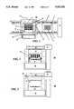
- FIG. 1is top view of a manufacturing line having a station in accordance with the present invention.
- FIG. 2is a top view of the station of FIG. 1 illustrating the bulk pouring of solder spheres onto a stencil in accordance with the present invention.
- FIG. 3is a top view of the station of FIG. 1 illustrating solder spheres covering the stencil in accordance with the present invention.
- FIG. 4is a top view of the station of FIG. 1 illustrating the start of the removal of the excess solder spheres off the stencil in accordance with the present invention.
- FIG. 5is a side cut-view of the station of FIG. 1 along line 5--5 of FIG. 4 showing a directed column of air used for plowing the excess solder balls off the stencil in accordance with the present invention.
- FIG. 6is a top view of the station of FIG. 1 illustrating another step in the removal of the solder spheres of the stencil in accordance with the present invention.
- FIG. 7is a side cut-view of the station of FIG. 1 along line 7--7 of FIG. 6 showing the removal of excess solder spheres and the placement of solder spheres within the apertures of the stencil in accordance with the present invention.
- FIG. 8is an enlarged side-cut view similar to FIG. 7 in accordance with the present invention.
- a station 10 in a manufacturing line 12for the accurate placement of solder balls or spheres on a ball grid array (BGA) carrier or package and for the removal of excess solder balls from the top surface of a stencil 16 once the solder spheres are set in place.
- the station 10preferably comprises a frame 14 having the stencil 16.
- the stencilpreferably has an array of apertures 18 that have diameters for allowing entry of one solder sphere per aperture. For example, stencil apertures having a diameter of 0.023" would be ideally suited for 0.020" diameter solder balls.
- the station 10further comprises a bulk dispenser/bin 26 of solder spheres which also serves as a reservoir for the excess solder spheres when they are removed from the stencil as will be shown.
- a pneumatic or alternatively a hydraulic lift 23can be used to lift the bin to dispense the solder spheres from the dispenser 26 and subsequently return the dispenser to its original position as a bin.
- the stationfurther comprises a means for urging the solder spheres into the apertures of the stencil such as a vibrating device 20.
- the vibrating deviceis preferably a low amplitude, low frequency vibrator.
- a pneumatic slide 22allows a directed column of air 24 (such as an Air Knife by EXAIR Corporation) to move across the surface of the stencil to remove excess solder balls as will be shown.
- the station 10preferably uses a pallet 2 to hold and transport (on rollers 11 ) a substrate 4 having solder pads that are previously fluxed to the frame 14.
- the fluxed substrate and palletare located and aligned with the matching BGA pattern of the stencil above. Once the solder spheres are placed on the substrate and the excess solder spheres removed from the stencil, the pallet transpods the BGA solder bumped substrate 6 on rollers 11 towards a next station such as a reflow oven 28.
- FIGS. 2-8the process of placing solder spheres onto a BGA substrate or carrier and the removal of excess balls from a stencil will be described in further detail.
- the bin/dispenser 26 in FIG. 2bulk pours solder spheres 30 onto the stencil 16 having the array of apertures 18.
- the vibrator 20is turned for several seconds to urge the solder spheres into the array of apertures 18.
- the pneumatic slide 22 and directed air column 24remain retracted at this point.
- FIG. 3illustrates how the solder spheres cover all the apertures or openings of the stencil after the vibration is provided.
- FIG. 5shows a side cut-view of the station of FIG. 1 along line 5--5 of FIG.
- the directed column of aircan be a series of through holes 27 or alternatively a single sleeved-shaped gap as used in the commercially available Air Knife by EXAIR Corporation.
- FIG. 7a side cut-view of the station of FIG. 1 along line 7--7 of FIG. 6 shows the removal of excess solder spheres and the placement of solder spheres within the apertures of the stencil in accordance with the present invention.
- the directed column of air originating from the series of holes 27(or alternatively from the sleeved shaped gap of an Air Knife) is mounted slightly above the stencil and directed down in an angular fashion as shown.
- the directed column of air 24serves as a plow in removing the remaining layers of solder balls and leaving the located spheres within their respective stencil apertures.
- the stencil 16is removed and the BGA solder bumped substrate 6 (See FIG. 1) is forwarded to the next station, preferably a reflow oven 28.
- FIG. 8a enlarged side-cut view is shown similar to FIG. 7.
- the top side of the stencil 16has a beveled periphery 15 around the apertures to provide a rounded contact area between the excess balls and the top of the stencil aperture. This reduces the likelihood of extra balls sticking to the surface when the directed column of air or an Air Knife passes over.
- This beveled periphery 15also makes it easier for the primary balls to locate themselves in the openings during vibration and onto the flux 8 above the solder pads 7.
- the bottom side of the stencilis "domed" (17) to provide extra clearance from the fluxed solder pad (7 and 8), since the solder spheres 30 have very little mass and will readily cling to any extra flux in the area.
- Nickel plating of the stencilcan also provide a slicker surface which is desirable when trying to blow off the excess solder spheres.
Landscapes
- Engineering & Computer Science (AREA)
- Manufacturing & Machinery (AREA)
- Microelectronics & Electronic Packaging (AREA)
- Mechanical Engineering (AREA)
- Ceramic Engineering (AREA)
- Physics & Mathematics (AREA)
- Condensed Matter Physics & Semiconductors (AREA)
- General Physics & Mathematics (AREA)
- Computer Hardware Design (AREA)
- Power Engineering (AREA)
- Electric Connection Of Electric Components To Printed Circuits (AREA)
Abstract
Description
Claims (23)
Priority Applications (1)
| Application Number | Priority Date | Filing Date | Title |
|---|---|---|---|
| US08/192,880US5431332A (en) | 1994-02-07 | 1994-02-07 | Method and apparatus for solder sphere placement using an air knife |
Applications Claiming Priority (1)
| Application Number | Priority Date | Filing Date | Title |
|---|---|---|---|
| US08/192,880US5431332A (en) | 1994-02-07 | 1994-02-07 | Method and apparatus for solder sphere placement using an air knife |
Publications (1)
| Publication Number | Publication Date |
|---|---|
| US5431332Atrue US5431332A (en) | 1995-07-11 |
Family
ID=22711400
Family Applications (1)
| Application Number | Title | Priority Date | Filing Date |
|---|---|---|---|
| US08/192,880Expired - Fee RelatedUS5431332A (en) | 1994-02-07 | 1994-02-07 | Method and apparatus for solder sphere placement using an air knife |
Country Status (1)
| Country | Link |
|---|---|
| US (1) | US5431332A (en) |
Cited By (120)
| Publication number | Priority date | Publication date | Assignee | Title |
|---|---|---|---|---|
| WO1997023903A1 (en)* | 1995-12-22 | 1997-07-03 | Tti Testron, Inc. | Method of placing contacts onto a substrate |
| US5655704A (en)* | 1994-08-30 | 1997-08-12 | Matsushita Electric Industrial Co., Ltd. | Method and apparatus for mounting soldering balls onto electrodes of a substrate or a comparable electronic component |
| US5685477A (en)* | 1995-06-28 | 1997-11-11 | Intel Corporation | Method for attaching and handling conductive spheres to a substrate |
| US5704536A (en)* | 1996-03-12 | 1998-01-06 | Industrial Technology Research Institute | Automatic ball placing device |
| EP0796200A4 (en)* | 1994-09-14 | 1998-05-27 | Vanguard Automation Inc | Method and apparatus for filling a ball grid array |
| US5768775A (en)* | 1995-08-24 | 1998-06-23 | Matsushita Electric Industrial Co., Ltd. | Mounting apparatus of conductive balls and mounting method thereof |
| WO1998033210A1 (en)* | 1997-01-24 | 1998-07-30 | Unisys Corporation | Vibrating template method of placing solder balls on the i/o pads of an integrated circuit package |
| WO1998036451A1 (en)* | 1997-02-18 | 1998-08-20 | Edm Supplies, Inc. | Method and apparatus for placing and attaching solder balls to substrates |
| US5816482A (en)* | 1996-04-26 | 1998-10-06 | The Whitaker Corporation | Method and apparatus for attaching balls to a substrate |
| WO1998047330A1 (en)* | 1997-04-11 | 1998-10-22 | Advanced Systems Automation Limited | Solder ball loading mechanism |
| US5831247A (en)* | 1995-06-19 | 1998-11-03 | Matsushita Electric Industrial Co., Ltd. | Apparatus and method for producing an electronic component provided with bumps |
| US5839641A (en)* | 1995-08-30 | 1998-11-24 | Industrial Technology Research Institute | Apparatus for placing and aligning solder balls onto solder pads on a substrate for manufacturing IC devices |
| US5857610A (en)* | 1995-11-14 | 1999-01-12 | Nippon Steel Corporation | Process and apparatus for forming ball bumps |
| US5861323A (en)* | 1994-06-06 | 1999-01-19 | Microfab Technologies, Inc. | Process for manufacturing metal ball electrodes for a semiconductor device |
| EP0902610A1 (en)* | 1997-09-10 | 1999-03-17 | STMicroelectronics S.r.l. | Arrangement of an ordered array of balls of solder alloy on respective pads of a baseplate of a BGA device |
| US5899376A (en)* | 1995-07-11 | 1999-05-04 | Nippon Steel Corporation | Transfer of flux onto electrodes and production of bumps on electrodes |
| US5914859A (en)* | 1996-04-29 | 1999-06-22 | Ibiden Co., Ltd. | Electronic component mounting base board and method of producing the same |
| US5918792A (en)* | 1997-04-04 | 1999-07-06 | Rvsi Vanguard, Inc. | Apparatus and method for filling a ball grid array |
| EP0840368A3 (en)* | 1996-10-30 | 1999-07-07 | E.I. Du Pont De Nemours And Company | Product and method for placing particles on contact pads of electronic devices |
| US5921458A (en)* | 1997-06-25 | 1999-07-13 | Fan; Kuang-Shu | Integrated circuit solder ball implant machine |
| US5938106A (en)* | 1996-08-01 | 1999-08-17 | International Business Machines Corporation | Method and apparatus for applying solder and forming solder balls on a substrate |
| US5985694A (en)* | 1997-09-29 | 1999-11-16 | Motorola, Inc. | Semiconductor die bumping method utilizing vacuum stencil |
| US6024584A (en)* | 1996-10-10 | 2000-02-15 | Berg Technology, Inc. | High density connector |
| EP0980198A1 (en)* | 1998-08-13 | 2000-02-16 | Bull S.A. | Detachable tool for making electrically conductive bumps on electronic components |
| US6034426A (en)* | 1997-10-30 | 2000-03-07 | Hewlett-Packard Co. | Testable low inductance integrated circuit package |
| US6042389A (en)* | 1996-10-10 | 2000-03-28 | Berg Technology, Inc. | Low profile connector |
| US6056190A (en)* | 1997-02-06 | 2000-05-02 | Speedline Technologies, Inc. | Solder ball placement apparatus |
| US6093035A (en)* | 1996-06-28 | 2000-07-25 | Berg Technology, Inc. | Contact for use in an electrical connector |
| US6099935A (en)* | 1995-12-15 | 2000-08-08 | International Business Machines Corporation | Apparatus for providing solder interconnections to semiconductor and electronic packaging devices |
| US6119927A (en)* | 1997-02-18 | 2000-09-19 | Edm Supplies, Inc. | Method and apparatus for placing and attaching solder balls to substrates |
| FR2791046A1 (en) | 1999-03-17 | 2000-09-22 | Novatec Sa Soc | Ball filling device of ball bumping apparatus used in forming ball grid array packages, has resilient track forming board to maintain single layer of solder balls in opening region of housing |
| US6138562A (en)* | 1998-01-20 | 2000-10-31 | Hertz; Allen D. | Vibrational energy waves for assist in the print release process for screen printing |
| US6139336A (en)* | 1996-11-14 | 2000-10-31 | Berg Technology, Inc. | High density connector having a ball type of contact surface |
| US6146203A (en)* | 1995-06-12 | 2000-11-14 | Berg Technology, Inc. | Low cross talk and impedance controlled electrical connector |
| US6162661A (en)* | 1997-05-30 | 2000-12-19 | Tessera, Inc. | Spacer plate solder ball placement fixture and methods therefor |
| US6170737B1 (en) | 1997-02-06 | 2001-01-09 | Speedline Technologies, Inc. | Solder ball placement method |
| EP0962969A3 (en)* | 1998-05-29 | 2001-01-10 | Hitachi, Ltd. | Method for forming bumps |
| US6182356B1 (en)* | 1997-11-24 | 2001-02-06 | International Business Machines Corporation | Apparatus for solder ball mold loading |
| US6191022B1 (en)* | 1999-04-18 | 2001-02-20 | Cts Corporation | Fine pitch solder sphere placement |
| US6202918B1 (en) | 1997-01-28 | 2001-03-20 | Eric Hertz | Method and apparatus for placing conductive preforms |
| US6204094B1 (en)* | 1998-02-04 | 2001-03-20 | Texas Instruments Incorporated | Method and apparatus for populating an adhesive sheet with particles |
| US6217989B1 (en) | 1999-12-10 | 2001-04-17 | International Business Machines Corporation | Conductive line features for enhanced reliability of multi-layer ceramic substrates |
| US6227437B1 (en) | 1999-08-24 | 2001-05-08 | Kulicke & Soffa Industries Inc. | Solder ball delivery and reflow apparatus and method of using the same |
| US6230963B1 (en) | 1997-01-28 | 2001-05-15 | Eric L. Hertz | Method and apparatus using colored foils for placing conductive preforms |
| US6234382B1 (en) | 1997-06-20 | 2001-05-22 | Meco Equipment Engineers B.V. | Method and device for bonding solder balls to a substrate |
| US6241535B1 (en) | 1996-10-10 | 2001-06-05 | Berg Technology, Inc. | Low profile connector |
| US6253992B1 (en)* | 1998-03-18 | 2001-07-03 | Tessera, Inc. | Solder ball placement fixtures and methods |
| US6268275B1 (en) | 1998-10-08 | 2001-07-31 | Micron Technology, Inc. | Method of locating conductive spheres utilizing screen and hopper of solder balls |
| US6270002B1 (en)* | 1997-09-10 | 2001-08-07 | Nippon Micrometal Co., Ltd. | Ball arrangement method and ball arrangement apparatus |
| US6276598B1 (en) | 1999-07-13 | 2001-08-21 | Asm Assembly Automation Ltd. | Method and apparatus for ball placement |
| US6325644B1 (en) | 1996-10-10 | 2001-12-04 | Berg Technology, Inc. | High density connector and method of manufacture |
| WO2002028584A1 (en)* | 2000-10-03 | 2002-04-11 | Visteon Global Technologies, Inc. | System and method for mounting electronic components onto flexible substrates |
| WO2002028583A1 (en)* | 2000-10-03 | 2002-04-11 | Visteon Global Technologies, Inc. | System and method for mounting electronic components onto flexible substrates |
| KR100332378B1 (en)* | 1999-09-11 | 2002-04-12 | 이병구 | Fluxless soldering method |
| US6386433B1 (en) | 1999-08-24 | 2002-05-14 | Kulicke & Soffa Investments, Inc. | Solder ball delivery and reflow apparatus and method |
| US6390351B1 (en)* | 1999-10-22 | 2002-05-21 | Matsushita Electric Industrial Co., Ltd. | Apparatus and method of transferring conductive balls and apparatus and method of supplying conductive balls |
| US6402014B1 (en) | 1998-05-29 | 2002-06-11 | Hitachi, Ltd. | Method of forming bumps |
| US6412685B2 (en) | 1997-01-28 | 2002-07-02 | Galahad, Co. | Method and apparatus for release and optional inspection for conductive preforms placement apparatus |
| US6415503B1 (en)* | 2000-12-08 | 2002-07-09 | Silitek Corporation | Assembling system of rubber cones of computer keyboards |
| US6426564B1 (en) | 1999-02-24 | 2002-07-30 | Micron Technology, Inc. | Recessed tape and method for forming a BGA assembly |
| US6460755B1 (en)* | 1996-03-08 | 2002-10-08 | Hitachi, Ltd. | Bump forming method and apparatus therefor |
| US6476486B1 (en) | 1997-10-30 | 2002-11-05 | Agilent Technologies, Inc. | Ball grid array package with supplemental electronic component |
| US6484927B1 (en)* | 1999-11-05 | 2002-11-26 | Delaware Capital Formation Corporation | Method and apparatus for balling and assembling ball grid array and chip scale array packages |
| US6533159B1 (en) | 1998-10-07 | 2003-03-18 | Micron Technology, Inc. | Apparatus for attaching solder balls to BGA package utilizing a tool to pick and dip the solder ball in flux |
| US20030070290A1 (en)* | 1998-09-03 | 2003-04-17 | Farnworth Warren M. | Methods of bonding solder balls to bond pads on a substrate, and bonding frames |
| US6604673B1 (en) | 1999-03-17 | 2003-08-12 | Novatec Sa | Filling device and method for filling balls in the apertures of a ball-receiving element |
| GB2386574A (en)* | 2002-03-20 | 2003-09-24 | Compeq Mfg Co Ltd | Solder paste stencilling apparatus for minimizing residue of solder waste |
| US6641030B1 (en) | 1997-02-06 | 2003-11-04 | Speedline Technologies, Inc. | Method and apparatus for placing solder balls on a substrate |
| US6642485B2 (en) | 2001-12-03 | 2003-11-04 | Visteon Global Technologies, Inc. | System and method for mounting electronic components onto flexible substrates |
| US20040050915A1 (en)* | 2001-10-03 | 2004-03-18 | Goenka Lakhi Nandlal | System and method for mounting electronic components onto flexible substrates |
| US6739498B2 (en)* | 2001-05-17 | 2004-05-25 | Intel Corporation | Solder ball attachment system |
| US20040126923A1 (en)* | 2002-12-31 | 2004-07-01 | Micron Technology, Inc. | Non-chemical, non-optical edge bead removal process |
| US20040149805A1 (en)* | 2003-02-05 | 2004-08-05 | Ito Carl T. | Solder ball dispenser |
| US20040169065A1 (en)* | 2001-09-07 | 2004-09-02 | Hans-Peter Caspar | Process and apparatus for applying brazing material to a metallic structure through the use of vibration |
| US20050001019A1 (en)* | 2003-05-07 | 2005-01-06 | Visteon Global Technologies, Inc. | Vector transient reflow of lead free solder for controlling substrate warpage |
| US6869008B2 (en) | 1998-05-29 | 2005-03-22 | Hitachi, Ltd. | Method of forming bumps |
| US20050085061A1 (en)* | 2002-07-18 | 2005-04-21 | Tsung-Hua Wu | Method of forming bumps |
| NL1024687C2 (en)* | 2003-11-03 | 2005-05-04 | Meco Equip Eng | Solder body positioning method for producing electrical contact device, comprises placing bodies in holder and supplying energy to them so that they become detached from holder |
| US6916731B2 (en)* | 1999-04-23 | 2005-07-12 | Nippon Steel Corporation | Ball transferring method and apparatus |
| US20050176176A1 (en)* | 2001-01-12 | 2005-08-11 | Nippon Steel Corporation | Ball transferring method and apparatus |
| US6939173B1 (en) | 1995-06-12 | 2005-09-06 | Fci Americas Technology, Inc. | Low cross talk and impedance controlled electrical connector with solder masses |
| US20050221675A1 (en)* | 2003-07-16 | 2005-10-06 | Rathburn James J | Fine pitch electrical interconnect assembly |
| US20050274770A1 (en)* | 2004-06-07 | 2005-12-15 | Henderson Marvin A Sr | Method for the precise and reliable placement of solid metallic and non-metallic particles |
| US20060035483A1 (en)* | 2003-07-16 | 2006-02-16 | Gryphics, Inc. | Fine pitch electrical interconnect assembly |
| GB2425502A (en)* | 2005-04-28 | 2006-11-01 | Shibuya Kogyo Co Ltd | Conductive ball mounting apparatus |
| US20070020909A1 (en)* | 2005-07-25 | 2007-01-25 | Stmicroelectronics S.A. | Forming of conductive bumps for an integrated circuit |
| US20070130764A1 (en)* | 2004-06-30 | 2007-06-14 | Athlete Fa Corporation | Method and apparatus for mounting conductive ball |
| US20080023528A1 (en)* | 2004-04-05 | 2008-01-31 | Wistron Corp. | Fabrication method and structure of pcb assembly, and tool for assembly thereof |
| US20080182436A1 (en)* | 2003-07-16 | 2008-07-31 | Gryphics, Inc. | Fine pitch electrical interconnect assembly |
| US20090020591A1 (en)* | 2007-07-19 | 2009-01-22 | Shinko Electric Industries Co., Ltd. | Conductive ball mounting method |
| US20090159646A1 (en)* | 2007-12-19 | 2009-06-25 | Shinko Electric Industries Co., Ltd. | Conductive ball removing method, conductive ball mounting method, conductive ball removing apparatus, and conductive ball mounting apparatus |
| US20090283575A1 (en)* | 2008-05-15 | 2009-11-19 | International Business Machines Corporation | Techniques for arranging solder balls and forming bumps |
| US20100037819A1 (en)* | 2008-08-14 | 2010-02-18 | Snu R&Db Foundation | Device for positioning nano materials |
| US20100127049A1 (en)* | 2007-05-08 | 2010-05-27 | Shinji Ishikawa | Solder ball mounting method and apparatus |
| US20100163605A1 (en)* | 2008-12-25 | 2010-07-01 | United Test Center Inc. | Ball implantation method and system applying the method |
| US20100230469A1 (en)* | 2007-03-07 | 2010-09-16 | Shinko Electric Industries Co., Ltd. | Conductive ball mounting apparatus and conductive ball mounting method |
| US8044502B2 (en) | 2006-03-20 | 2011-10-25 | Gryphics, Inc. | Composite contact for fine pitch electrical interconnect assembly |
| US8561880B2 (en)* | 2012-02-11 | 2013-10-22 | International Business Machines Corporation | Forming metal preforms and metal balls |
| US8833636B2 (en) | 2012-10-18 | 2014-09-16 | International Business Machines Corporation | Forming an array of metal balls or shapes on a substrate |
| US8875978B2 (en) | 2012-02-11 | 2014-11-04 | International Business Machines Corporation | Forming constant diameter spherical metal balls |
| USD718253S1 (en) | 2012-04-13 | 2014-11-25 | Fci Americas Technology Llc | Electrical cable connector |
| US8905651B2 (en) | 2012-01-31 | 2014-12-09 | Fci | Dismountable optical coupling device |
| USD720698S1 (en) | 2013-03-15 | 2015-01-06 | Fci Americas Technology Llc | Electrical cable connector |
| US8944831B2 (en) | 2012-04-13 | 2015-02-03 | Fci Americas Technology Llc | Electrical connector having ribbed ground plate with engagement members |
| USD727268S1 (en) | 2012-04-13 | 2015-04-21 | Fci Americas Technology Llc | Vertical electrical connector |
| USD727852S1 (en) | 2012-04-13 | 2015-04-28 | Fci Americas Technology Llc | Ground shield for a right angle electrical connector |
| US9048583B2 (en) | 2009-03-19 | 2015-06-02 | Fci Americas Technology Llc | Electrical connector having ribbed ground plate |
| USD733662S1 (en) | 2013-01-25 | 2015-07-07 | Fci Americas Technology Llc | Connector housing for electrical connector |
| USD746236S1 (en) | 2012-07-11 | 2015-12-29 | Fci Americas Technology Llc | Electrical connector housing |
| EP2947683A3 (en)* | 2014-05-21 | 2015-12-30 | Broadcom Corporation | Reconstituted interposer semiconductor package |
| US9257778B2 (en) | 2012-04-13 | 2016-02-09 | Fci Americas Technology | High speed electrical connector |
| US9543703B2 (en) | 2012-07-11 | 2017-01-10 | Fci Americas Technology Llc | Electrical connector with reduced stack height |
| US20180005976A1 (en)* | 2013-07-17 | 2018-01-04 | Taiwan Semiconductor Manufacturing Company, Ltd. | Mechanisms For Forming Bonding Structures |
| CZ307441B6 (en)* | 2017-08-25 | 2018-08-22 | Vysoké Učení Technické V Brně | A method of forming solder spherical outlets on a housing of an electronic component by means of a template and a template for implementing this method |
| CN105873378B (en)* | 2016-06-01 | 2018-12-21 | 全讯射频科技(无锡)有限公司 | The height adjustment device of a plant ball steel mesh |
| US10369648B2 (en)* | 2017-01-13 | 2019-08-06 | Horng Terng Automation Co., Ltd. | Guiding board for a ball placement machine |
| US10879102B2 (en)* | 2017-08-07 | 2020-12-29 | Boston Process Technologies, Inc | Flux-free solder ball mount arrangement |
| CN112259478A (en)* | 2020-10-23 | 2021-01-22 | 技感半导体设备(南通)有限公司 | Ball scraping and spreading device and method |
| WO2023129538A1 (en)* | 2021-12-28 | 2023-07-06 | Medtronic, Inc. | Electrical component and method of forming same |
| WO2023129537A3 (en)* | 2021-12-28 | 2023-08-10 | Medtronic, Inc. | Electrical component and method of forming same |
Citations (8)
| Publication number | Priority date | Publication date | Assignee | Title |
|---|---|---|---|---|
| US4462534A (en)* | 1981-12-29 | 1984-07-31 | International Business Machines Corporation | Method of bonding connecting pins to the eyelets of conductors formed on a ceramic substrate |
| US4830264A (en)* | 1986-10-08 | 1989-05-16 | International Business Machines Corporation | Method of forming solder terminals for a pinless ceramic module |
| US4871110A (en)* | 1987-09-14 | 1989-10-03 | Hitachi, Ltd. | Method and apparatus for aligning solder balls |
| US4940181A (en)* | 1989-04-06 | 1990-07-10 | Motorola, Inc. | Pad grid array for receiving a solder bumped chip carrier |
| US5024372A (en)* | 1989-01-03 | 1991-06-18 | Motorola, Inc. | Method of making high density solder bumps and a substrate socket for high density solder bumps |
| US5159171A (en)* | 1991-09-03 | 1992-10-27 | Motorola, Inc. | Method and apparatus for solder laser printing |
| US5205896A (en)* | 1992-02-03 | 1993-04-27 | Hughes Aircraft Company | Component and solder preform placement device and method of placement |
| US5255839A (en)* | 1992-01-02 | 1993-10-26 | Motorola, Inc. | Method for solder application and reflow |
- 1994
- 1994-02-07USUS08/192,880patent/US5431332A/ennot_activeExpired - Fee Related
Patent Citations (8)
| Publication number | Priority date | Publication date | Assignee | Title |
|---|---|---|---|---|
| US4462534A (en)* | 1981-12-29 | 1984-07-31 | International Business Machines Corporation | Method of bonding connecting pins to the eyelets of conductors formed on a ceramic substrate |
| US4830264A (en)* | 1986-10-08 | 1989-05-16 | International Business Machines Corporation | Method of forming solder terminals for a pinless ceramic module |
| US4871110A (en)* | 1987-09-14 | 1989-10-03 | Hitachi, Ltd. | Method and apparatus for aligning solder balls |
| US5024372A (en)* | 1989-01-03 | 1991-06-18 | Motorola, Inc. | Method of making high density solder bumps and a substrate socket for high density solder bumps |
| US4940181A (en)* | 1989-04-06 | 1990-07-10 | Motorola, Inc. | Pad grid array for receiving a solder bumped chip carrier |
| US5159171A (en)* | 1991-09-03 | 1992-10-27 | Motorola, Inc. | Method and apparatus for solder laser printing |
| US5255839A (en)* | 1992-01-02 | 1993-10-26 | Motorola, Inc. | Method for solder application and reflow |
| US5205896A (en)* | 1992-02-03 | 1993-04-27 | Hughes Aircraft Company | Component and solder preform placement device and method of placement |
Cited By (213)
| Publication number | Priority date | Publication date | Assignee | Title |
|---|---|---|---|---|
| US5861323A (en)* | 1994-06-06 | 1999-01-19 | Microfab Technologies, Inc. | Process for manufacturing metal ball electrodes for a semiconductor device |
| US5655704A (en)* | 1994-08-30 | 1997-08-12 | Matsushita Electric Industrial Co., Ltd. | Method and apparatus for mounting soldering balls onto electrodes of a substrate or a comparable electronic component |
| EP0796200A4 (en)* | 1994-09-14 | 1998-05-27 | Vanguard Automation Inc | Method and apparatus for filling a ball grid array |
| US6939173B1 (en) | 1995-06-12 | 2005-09-06 | Fci Americas Technology, Inc. | Low cross talk and impedance controlled electrical connector with solder masses |
| US6146203A (en)* | 1995-06-12 | 2000-11-14 | Berg Technology, Inc. | Low cross talk and impedance controlled electrical connector |
| US5831247A (en)* | 1995-06-19 | 1998-11-03 | Matsushita Electric Industrial Co., Ltd. | Apparatus and method for producing an electronic component provided with bumps |
| US5844316A (en)* | 1995-06-28 | 1998-12-01 | Intel Corporation | Fixture for handling and attaching conductive spheres to a substrate |
| US5685477A (en)* | 1995-06-28 | 1997-11-11 | Intel Corporation | Method for attaching and handling conductive spheres to a substrate |
| US5899376A (en)* | 1995-07-11 | 1999-05-04 | Nippon Steel Corporation | Transfer of flux onto electrodes and production of bumps on electrodes |
| US5768775A (en)* | 1995-08-24 | 1998-06-23 | Matsushita Electric Industrial Co., Ltd. | Mounting apparatus of conductive balls and mounting method thereof |
| US5839641A (en)* | 1995-08-30 | 1998-11-24 | Industrial Technology Research Institute | Apparatus for placing and aligning solder balls onto solder pads on a substrate for manufacturing IC devices |
| US5857610A (en)* | 1995-11-14 | 1999-01-12 | Nippon Steel Corporation | Process and apparatus for forming ball bumps |
| US6099935A (en)* | 1995-12-15 | 2000-08-08 | International Business Machines Corporation | Apparatus for providing solder interconnections to semiconductor and electronic packaging devices |
| WO1997023903A1 (en)* | 1995-12-22 | 1997-07-03 | Tti Testron, Inc. | Method of placing contacts onto a substrate |
| US6460755B1 (en)* | 1996-03-08 | 2002-10-08 | Hitachi, Ltd. | Bump forming method and apparatus therefor |
| US5704536A (en)* | 1996-03-12 | 1998-01-06 | Industrial Technology Research Institute | Automatic ball placing device |
| US5816482A (en)* | 1996-04-26 | 1998-10-06 | The Whitaker Corporation | Method and apparatus for attaching balls to a substrate |
| US5914859A (en)* | 1996-04-29 | 1999-06-22 | Ibiden Co., Ltd. | Electronic component mounting base board and method of producing the same |
| US6093035A (en)* | 1996-06-28 | 2000-07-25 | Berg Technology, Inc. | Contact for use in an electrical connector |
| US5938106A (en)* | 1996-08-01 | 1999-08-17 | International Business Machines Corporation | Method and apparatus for applying solder and forming solder balls on a substrate |
| US6027006A (en)* | 1996-08-01 | 2000-02-22 | International Business Machines Corporation | Method and apparatus for applying solder and forming solder balls on a substrate |
| US6241535B1 (en) | 1996-10-10 | 2001-06-05 | Berg Technology, Inc. | Low profile connector |
| US6325644B1 (en) | 1996-10-10 | 2001-12-04 | Berg Technology, Inc. | High density connector and method of manufacture |
| US6024584A (en)* | 1996-10-10 | 2000-02-15 | Berg Technology, Inc. | High density connector |
| US8167630B2 (en) | 1996-10-10 | 2012-05-01 | Fci Americas Technology Llc | High density connector and method of manufacture |
| US6358068B1 (en) | 1996-10-10 | 2002-03-19 | Fci Americas Technology, Inc. | Stress resistant connector and method for reducing stress in housing thereof |
| US7186123B2 (en) | 1996-10-10 | 2007-03-06 | Fci Americas Technology, Inc. | High density connector and method of manufacture |
| US6042389A (en)* | 1996-10-10 | 2000-03-28 | Berg Technology, Inc. | Low profile connector |
| US7476110B2 (en) | 1996-10-10 | 2009-01-13 | Fci Americas Technology, Inc. | High density connector and method of manufacture |
| US6079991A (en)* | 1996-10-10 | 2000-06-27 | Berg Technology, Inc. | Method for placing contact on electrical connector |
| US6164983A (en)* | 1996-10-10 | 2000-12-26 | Berg Technology, Inc. | High density connector |
| EP0840368A3 (en)* | 1996-10-30 | 1999-07-07 | E.I. Du Pont De Nemours And Company | Product and method for placing particles on contact pads of electronic devices |
| US6247635B1 (en) | 1996-11-14 | 2001-06-19 | Berg Technology, Inc. | High density connector having a ball type of contact surface |
| US6139336A (en)* | 1996-11-14 | 2000-10-31 | Berg Technology, Inc. | High density connector having a ball type of contact surface |
| WO1998033210A1 (en)* | 1997-01-24 | 1998-07-30 | Unisys Corporation | Vibrating template method of placing solder balls on the i/o pads of an integrated circuit package |
| US6412685B2 (en) | 1997-01-28 | 2002-07-02 | Galahad, Co. | Method and apparatus for release and optional inspection for conductive preforms placement apparatus |
| US6202918B1 (en) | 1997-01-28 | 2001-03-20 | Eric Hertz | Method and apparatus for placing conductive preforms |
| US6230963B1 (en) | 1997-01-28 | 2001-05-15 | Eric L. Hertz | Method and apparatus using colored foils for placing conductive preforms |
| US6427903B1 (en) | 1997-02-06 | 2002-08-06 | Speedline Technologies, Inc. | Solder ball placement apparatus |
| US6170737B1 (en) | 1997-02-06 | 2001-01-09 | Speedline Technologies, Inc. | Solder ball placement method |
| US6641030B1 (en) | 1997-02-06 | 2003-11-04 | Speedline Technologies, Inc. | Method and apparatus for placing solder balls on a substrate |
| US6056190A (en)* | 1997-02-06 | 2000-05-02 | Speedline Technologies, Inc. | Solder ball placement apparatus |
| WO1998036451A1 (en)* | 1997-02-18 | 1998-08-20 | Edm Supplies, Inc. | Method and apparatus for placing and attaching solder balls to substrates |
| US6119927A (en)* | 1997-02-18 | 2000-09-19 | Edm Supplies, Inc. | Method and apparatus for placing and attaching solder balls to substrates |
| US5918792A (en)* | 1997-04-04 | 1999-07-06 | Rvsi Vanguard, Inc. | Apparatus and method for filling a ball grid array |
| WO1998047330A1 (en)* | 1997-04-11 | 1998-10-22 | Advanced Systems Automation Limited | Solder ball loading mechanism |
| US6162661A (en)* | 1997-05-30 | 2000-12-19 | Tessera, Inc. | Spacer plate solder ball placement fixture and methods therefor |
| US6234382B1 (en) | 1997-06-20 | 2001-05-22 | Meco Equipment Engineers B.V. | Method and device for bonding solder balls to a substrate |
| US5921458A (en)* | 1997-06-25 | 1999-07-13 | Fan; Kuang-Shu | Integrated circuit solder ball implant machine |
| US6270002B1 (en)* | 1997-09-10 | 2001-08-07 | Nippon Micrometal Co., Ltd. | Ball arrangement method and ball arrangement apparatus |
| EP0902610A1 (en)* | 1997-09-10 | 1999-03-17 | STMicroelectronics S.r.l. | Arrangement of an ordered array of balls of solder alloy on respective pads of a baseplate of a BGA device |
| US5985694A (en)* | 1997-09-29 | 1999-11-16 | Motorola, Inc. | Semiconductor die bumping method utilizing vacuum stencil |
| US6476486B1 (en) | 1997-10-30 | 2002-11-05 | Agilent Technologies, Inc. | Ball grid array package with supplemental electronic component |
| US6034426A (en)* | 1997-10-30 | 2000-03-07 | Hewlett-Packard Co. | Testable low inductance integrated circuit package |
| US6182356B1 (en)* | 1997-11-24 | 2001-02-06 | International Business Machines Corporation | Apparatus for solder ball mold loading |
| US6745450B1 (en) | 1997-11-24 | 2004-06-08 | International Business Machines Corporation | Method for loading solder balls into a mold |
| US6138562A (en)* | 1998-01-20 | 2000-10-31 | Hertz; Allen D. | Vibrational energy waves for assist in the print release process for screen printing |
| US6204094B1 (en)* | 1998-02-04 | 2001-03-20 | Texas Instruments Incorporated | Method and apparatus for populating an adhesive sheet with particles |
| US6253992B1 (en)* | 1998-03-18 | 2001-07-03 | Tessera, Inc. | Solder ball placement fixtures and methods |
| US6213386B1 (en)* | 1998-05-29 | 2001-04-10 | Hitachi, Ltd. | Method of forming bumps |
| US6869008B2 (en) | 1998-05-29 | 2005-03-22 | Hitachi, Ltd. | Method of forming bumps |
| EP0962969A3 (en)* | 1998-05-29 | 2001-01-10 | Hitachi, Ltd. | Method for forming bumps |
| KR100495024B1 (en)* | 1998-05-29 | 2005-06-14 | 가부시키가이샤 히타치세이사쿠쇼 | A method for forming the bump |
| US6402014B1 (en) | 1998-05-29 | 2002-06-11 | Hitachi, Ltd. | Method of forming bumps |
| EP0980198A1 (en)* | 1998-08-13 | 2000-02-16 | Bull S.A. | Detachable tool for making electrically conductive bumps on electronic components |
| FR2782439A1 (en)* | 1998-08-13 | 2000-02-18 | Bull Sa | REMOVABLE TOOLS FOR MAKING BOSSES, ELECTRICAL CONDUCTORS, ON ELECTRONIC COMPONENTS |
| US6857183B2 (en) | 1998-09-03 | 2005-02-22 | Micron Technology, Inc. | Methods of bonding solder balls to bond pads on a substrate, and bonding frames |
| US20030070290A1 (en)* | 1998-09-03 | 2003-04-17 | Farnworth Warren M. | Methods of bonding solder balls to bond pads on a substrate, and bonding frames |
| US7591069B2 (en) | 1998-09-03 | 2009-09-22 | Micron Technology, Inc. | Methods of bonding solder balls to bond pads on a substrate, and bonding frames |
| US6705513B1 (en)* | 1998-09-03 | 2004-03-16 | Micron Technology, Inc. | Methods of bonding solder balls to bond pads on a substrate, and bonding frames |
| US6839961B2 (en) | 1998-09-03 | 2005-01-11 | Micron Technology, Inc. | Methods of bonding solder balls to bond pads on a substrate, and bonding frames |
| US7003874B1 (en) | 1998-09-03 | 2006-02-28 | Micron Technology, Inc. | Methods of bonding solder balls to bond pads on a substrate |
| US20050023259A1 (en)* | 1998-09-03 | 2005-02-03 | Farnworh Warren M. | Methods of bonding solder balls to bond pads on a substrate, and bonding frames |
| US20030111508A1 (en)* | 1998-10-07 | 2003-06-19 | Cobbley Chad A. | Apparatus for attaching solder balls to BGA package utilizing a tool to pick and dip the solder ball in flux |
| US20060027624A1 (en)* | 1998-10-07 | 2006-02-09 | Cobbley Chad A | Apparatus for attaching solder balls to BGA package utilizing a tool to pick and dip the solder ball in flux |
| US6844216B2 (en) | 1998-10-07 | 2005-01-18 | Micron Technology, Inc. | Method of attaching solder balls to BGA package utilizing a tool to pick and dip the solder ball in flux |
| US6533159B1 (en) | 1998-10-07 | 2003-03-18 | Micron Technology, Inc. | Apparatus for attaching solder balls to BGA package utilizing a tool to pick and dip the solder ball in flux |
| US6957760B2 (en) | 1998-10-07 | 2005-10-25 | Micron Technology, Inc. | Apparatus for attaching solder balls to BGA package utilizing a tool to pick and dip the solder ball in flux |
| US6595408B1 (en) | 1998-10-07 | 2003-07-22 | Micron Technology, Inc. | Method of attaching solder balls to BGA package utilizing a tool to pick and dip the solder ball in flux prior to placement |
| US7644853B2 (en) | 1998-10-07 | 2010-01-12 | Micron Technology, Inc. | Apparatus for attaching solder balls to BGA package utilizing a tool to pick and dip the solder ball in flux |
| US20030121957A1 (en)* | 1998-10-07 | 2003-07-03 | Cobbley Chad A. | Method of attaching solder balls to BGA package utilizing a tool to pick and dip the solder ball in flux |
| US20030110626A1 (en)* | 1998-10-08 | 2003-06-19 | Cobbley Chad A. | Method of locating conductive spheres utilizing screen and hopper of solder balls |
| US6551917B2 (en) | 1998-10-08 | 2003-04-22 | Micron Technology, Inc. | Method of locating conductive spheres utilizing screen and hopper of solder balls |
| US20050056682A1 (en)* | 1998-10-08 | 2005-03-17 | Cobbley Chad A. | Method of locating conductive spheres utilizing screen and hopper of solder balls |
| US20050056681A1 (en)* | 1998-10-08 | 2005-03-17 | Cobbley Chad A. | Method of locating conductive spheres utilizing screen and hopper of solder balls |
| US6268275B1 (en) | 1998-10-08 | 2001-07-31 | Micron Technology, Inc. | Method of locating conductive spheres utilizing screen and hopper of solder balls |
| US7275676B2 (en) | 1998-10-08 | 2007-10-02 | Micron Technology, Inc. | Apparatus for locating conductive spheres utilizing screen and hopper of solder balls |
| US7105432B2 (en) | 1998-10-08 | 2006-09-12 | Micron Technology, Inc. | Method of locating conductive spheres utilizing screen and hopper of solder balls |
| US7635079B1 (en) | 1998-10-08 | 2009-12-22 | Micron Technology, Inc. | System for locating conductive sphere utilizing screen and hopper of solder balls |
| US6855623B2 (en)* | 1999-02-24 | 2005-02-15 | Micron Technology Inc. | Recessed tape and method for forming a BGA assembly |
| US20020192936A1 (en)* | 1999-02-24 | 2002-12-19 | Micron Technology, Inc. | Recessed tape and method for forming a BGA assembly |
| US6426564B1 (en) | 1999-02-24 | 2002-07-30 | Micron Technology, Inc. | Recessed tape and method for forming a BGA assembly |
| US7455209B2 (en) | 1999-03-17 | 2008-11-25 | Novatec Sa | Filling device and method for filling balls in the apertures of a ball-receiving element |
| US20040035908A1 (en)* | 1999-03-17 | 2004-02-26 | Novatec Sa | Filling device and method for filling balls in the apertures of a ball-receiving element |
| FR2791046A1 (en) | 1999-03-17 | 2000-09-22 | Novatec Sa Soc | Ball filling device of ball bumping apparatus used in forming ball grid array packages, has resilient track forming board to maintain single layer of solder balls in opening region of housing |
| US6604673B1 (en) | 1999-03-17 | 2003-08-12 | Novatec Sa | Filling device and method for filling balls in the apertures of a ball-receiving element |
| US6191022B1 (en)* | 1999-04-18 | 2001-02-20 | Cts Corporation | Fine pitch solder sphere placement |
| US6916731B2 (en)* | 1999-04-23 | 2005-07-12 | Nippon Steel Corporation | Ball transferring method and apparatus |
| US6276598B1 (en) | 1999-07-13 | 2001-08-21 | Asm Assembly Automation Ltd. | Method and apparatus for ball placement |
| US6227437B1 (en) | 1999-08-24 | 2001-05-08 | Kulicke & Soffa Industries Inc. | Solder ball delivery and reflow apparatus and method of using the same |
| US6634545B2 (en) | 1999-08-24 | 2003-10-21 | Kulicke & Soffa Investments, Inc. | Solder ball delivery and reflow method |
| US6386433B1 (en) | 1999-08-24 | 2002-05-14 | Kulicke & Soffa Investments, Inc. | Solder ball delivery and reflow apparatus and method |
| KR100332378B1 (en)* | 1999-09-11 | 2002-04-12 | 이병구 | Fluxless soldering method |
| US6390351B1 (en)* | 1999-10-22 | 2002-05-21 | Matsushita Electric Industrial Co., Ltd. | Apparatus and method of transferring conductive balls and apparatus and method of supplying conductive balls |
| US6484927B1 (en)* | 1999-11-05 | 2002-11-26 | Delaware Capital Formation Corporation | Method and apparatus for balling and assembling ball grid array and chip scale array packages |
| US6348233B2 (en) | 1999-12-10 | 2002-02-19 | International Business Machines Corporation | Method of forming conductive line features for enhanced reliability of multi-layer ceramic substrates |
| US6217989B1 (en) | 1999-12-10 | 2001-04-17 | International Business Machines Corporation | Conductive line features for enhanced reliability of multi-layer ceramic substrates |
| WO2002028583A1 (en)* | 2000-10-03 | 2002-04-11 | Visteon Global Technologies, Inc. | System and method for mounting electronic components onto flexible substrates |
| GB2372006B (en)* | 2000-10-03 | 2004-04-21 | Visteon Global Tech Inc | System and method for mounting electronic components onto flexible substrates |
| GB2372006A (en)* | 2000-10-03 | 2002-08-14 | Visteon Global Tech Inc | System and method for mounting electronic components onto flexible substrates |
| US20040094607A1 (en)* | 2000-10-03 | 2004-05-20 | Goenka Lakhi N. | System and method for mounting electronic components onto flexible substrates |
| GB2372228B (en)* | 2000-10-03 | 2004-07-21 | Visteon Global Tech Inc | System and method for mounting electronic components onto flexible substrates |
| US7156279B2 (en) | 2000-10-03 | 2007-01-02 | Visteon Global Technologie, Inc. | System and method for mounting electronic components onto flexible substrates |
| GB2372228A (en)* | 2000-10-03 | 2002-08-21 | Visteon Global Tech Inc | System and method for mounting electronic components onto flexible substrates |
| WO2002028584A1 (en)* | 2000-10-03 | 2002-04-11 | Visteon Global Technologies, Inc. | System and method for mounting electronic components onto flexible substrates |
| US6415503B1 (en)* | 2000-12-08 | 2002-07-09 | Silitek Corporation | Assembling system of rubber cones of computer keyboards |
| US20050176176A1 (en)* | 2001-01-12 | 2005-08-11 | Nippon Steel Corporation | Ball transferring method and apparatus |
| US20080032495A1 (en)* | 2001-01-12 | 2008-02-07 | Nippon Steel Materials Co., Ltd. | Ball transferring method and apparatus |
| US7285486B2 (en) | 2001-01-12 | 2007-10-23 | Nippon Steel Materials Co., Ltd. | Ball transferring method and apparatus |
| US6739498B2 (en)* | 2001-05-17 | 2004-05-25 | Intel Corporation | Solder ball attachment system |
| US6905059B2 (en) | 2001-05-17 | 2005-06-14 | Intel Corporation | Solder ball attachment system |
| US20040182910A1 (en)* | 2001-05-17 | 2004-09-23 | Intel Corporation | Solder ball attachment system |
| US20040169065A1 (en)* | 2001-09-07 | 2004-09-02 | Hans-Peter Caspar | Process and apparatus for applying brazing material to a metallic structure through the use of vibration |
| US7073700B2 (en)* | 2001-09-07 | 2006-07-11 | Emitec Gesellschaft Fuer Emissionstechnologie Mbh | Process and apparatus for applying brazing material to a metallic structure through the use of vibration |
| US20040050915A1 (en)* | 2001-10-03 | 2004-03-18 | Goenka Lakhi Nandlal | System and method for mounting electronic components onto flexible substrates |
| US6642485B2 (en) | 2001-12-03 | 2003-11-04 | Visteon Global Technologies, Inc. | System and method for mounting electronic components onto flexible substrates |
| GB2386574B (en)* | 2002-03-20 | 2004-09-08 | Compeq Mfg Co Ltd | Solder paste stenciling apparatus |
| GB2386574A (en)* | 2002-03-20 | 2003-09-24 | Compeq Mfg Co Ltd | Solder paste stencilling apparatus for minimizing residue of solder waste |
| US7375020B2 (en)* | 2002-07-18 | 2008-05-20 | Advanced Semiconductor Engineering, Inc. | Method of forming bumps |
| US20050085061A1 (en)* | 2002-07-18 | 2005-04-21 | Tsung-Hua Wu | Method of forming bumps |
| US20040126923A1 (en)* | 2002-12-31 | 2004-07-01 | Micron Technology, Inc. | Non-chemical, non-optical edge bead removal process |
| US8192555B2 (en) | 2002-12-31 | 2012-06-05 | Micron Technology, Inc. | Non-chemical, non-optical edge bead removal process |
| US8641831B2 (en) | 2002-12-31 | 2014-02-04 | Micron Technology, Inc. | Non-chemical, non-optical edge bead removal process |
| US6830175B2 (en) | 2003-02-05 | 2004-12-14 | Carl T. Ito | Solder ball dispenser |
| US20040149805A1 (en)* | 2003-02-05 | 2004-08-05 | Ito Carl T. | Solder ball dispenser |
| US20050001019A1 (en)* | 2003-05-07 | 2005-01-06 | Visteon Global Technologies, Inc. | Vector transient reflow of lead free solder for controlling substrate warpage |
| US7026582B2 (en) | 2003-05-07 | 2006-04-11 | Visteon Global Technologies, Inc. | Vector transient reflow of lead free solder for controlling substrate warpage |
| US7326064B2 (en) | 2003-07-16 | 2008-02-05 | Gryphics, Inc. | Fine pitch electrical interconnect assembly |
| US20050221675A1 (en)* | 2003-07-16 | 2005-10-06 | Rathburn James J | Fine pitch electrical interconnect assembly |
| US20080182436A1 (en)* | 2003-07-16 | 2008-07-31 | Gryphics, Inc. | Fine pitch electrical interconnect assembly |
| US7422439B2 (en) | 2003-07-16 | 2008-09-09 | Gryphics, Inc. | Fine pitch electrical interconnect assembly |
| US20060035483A1 (en)* | 2003-07-16 | 2006-02-16 | Gryphics, Inc. | Fine pitch electrical interconnect assembly |
| US7537461B2 (en) | 2003-07-16 | 2009-05-26 | Gryphics, Inc. | Fine pitch electrical interconnect assembly |
| US7297003B2 (en) | 2003-07-16 | 2007-11-20 | Gryphics, Inc. | Fine pitch electrical interconnect assembly |
| NL1024687C2 (en)* | 2003-11-03 | 2005-05-04 | Meco Equip Eng | Solder body positioning method for producing electrical contact device, comprises placing bodies in holder and supplying energy to them so that they become detached from holder |
| US20080023528A1 (en)* | 2004-04-05 | 2008-01-31 | Wistron Corp. | Fabrication method and structure of pcb assembly, and tool for assembly thereof |
| US7665648B2 (en)* | 2004-04-05 | 2010-02-23 | Wistron Corp. | Fabrication method and structure of PCB assembly, and tool for assembly thereof |
| US20050274770A1 (en)* | 2004-06-07 | 2005-12-15 | Henderson Marvin A Sr | Method for the precise and reliable placement of solid metallic and non-metallic particles |
| US20070130764A1 (en)* | 2004-06-30 | 2007-06-14 | Athlete Fa Corporation | Method and apparatus for mounting conductive ball |
| US20090307899A1 (en)* | 2004-06-30 | 2009-12-17 | Athlete Fa Corporation | Method and apparatus for mounting conductive balls |
| US8387236B2 (en) | 2004-06-30 | 2013-03-05 | Athlete Fa Corporation | Apparatus for mounting conductive balls |
| US8074867B2 (en) | 2005-04-28 | 2011-12-13 | Shibuya Kogyo Co., Ltd. | Conductive ball mounting apparatus |
| US20060244155A1 (en)* | 2005-04-28 | 2006-11-02 | Shibuya Kogyo Co., Ltd | Conductive ball mounting apparatus |
| GB2425502A (en)* | 2005-04-28 | 2006-11-01 | Shibuya Kogyo Co Ltd | Conductive ball mounting apparatus |
| US20100127048A1 (en)* | 2005-04-28 | 2010-05-27 | Shibuya Kogyo Co., Ltd. | Conductive ball mounting apparatus |
| GB2425502B (en)* | 2005-04-28 | 2010-06-16 | Shibuya Kogyo Co Ltd | Conductive ball mounting apparatus |
| US20070020909A1 (en)* | 2005-07-25 | 2007-01-25 | Stmicroelectronics S.A. | Forming of conductive bumps for an integrated circuit |
| US8232632B2 (en) | 2006-03-20 | 2012-07-31 | R&D Sockets, Inc. | Composite contact for fine pitch electrical interconnect assembly |
| US8044502B2 (en) | 2006-03-20 | 2011-10-25 | Gryphics, Inc. | Composite contact for fine pitch electrical interconnect assembly |
| US7900807B2 (en)* | 2007-03-07 | 2011-03-08 | Shinko Electric Industries Co., Ltd. | Conductive ball mounting apparatus and conductive ball mounting method |
| US20100230469A1 (en)* | 2007-03-07 | 2010-09-16 | Shinko Electric Industries Co., Ltd. | Conductive ball mounting apparatus and conductive ball mounting method |
| US20100127049A1 (en)* | 2007-05-08 | 2010-05-27 | Shinji Ishikawa | Solder ball mounting method and apparatus |
| US8104663B2 (en)* | 2007-05-08 | 2012-01-31 | Nippon Steel Materials Co., Ltd. | Solder ball mounting method and apparatus |
| US7820479B2 (en)* | 2007-07-19 | 2010-10-26 | Shinko Electric Industries Co., Ltd. | Conductive ball mounting method |
| US20090020591A1 (en)* | 2007-07-19 | 2009-01-22 | Shinko Electric Industries Co., Ltd. | Conductive ball mounting method |
| US7866533B2 (en)* | 2007-12-19 | 2011-01-11 | Shinko Electric Industries Co., Ltd. | Conductive ball removing method, conductive ball mounting method, conductive ball removing apparatus, and conductive ball mounting apparatus |
| US20090159646A1 (en)* | 2007-12-19 | 2009-06-25 | Shinko Electric Industries Co., Ltd. | Conductive ball removing method, conductive ball mounting method, conductive ball removing apparatus, and conductive ball mounting apparatus |
| US20090283575A1 (en)* | 2008-05-15 | 2009-11-19 | International Business Machines Corporation | Techniques for arranging solder balls and forming bumps |
| US7891538B2 (en) | 2008-05-15 | 2011-02-22 | International Business Machines Corporation | Techniques for arranging solder balls and forming bumps |
| US8087566B2 (en)* | 2008-05-15 | 2012-01-03 | International Business Machines Corporation | Techniques for arranging solder balls and forming bumps |
| US7780063B2 (en)* | 2008-05-15 | 2010-08-24 | International Business Machines Corporation | Techniques for arranging solder balls and forming bumps |
| US20100037819A1 (en)* | 2008-08-14 | 2010-02-18 | Snu R&Db Foundation | Device for positioning nano materials |
| US20100163605A1 (en)* | 2008-12-25 | 2010-07-01 | United Test Center Inc. | Ball implantation method and system applying the method |
| US10720721B2 (en) | 2009-03-19 | 2020-07-21 | Fci Usa Llc | Electrical connector having ribbed ground plate |
| US9048583B2 (en) | 2009-03-19 | 2015-06-02 | Fci Americas Technology Llc | Electrical connector having ribbed ground plate |
| US10096921B2 (en) | 2009-03-19 | 2018-10-09 | Fci Usa Llc | Electrical connector having ribbed ground plate |
| US9461410B2 (en) | 2009-03-19 | 2016-10-04 | Fci Americas Technology Llc | Electrical connector having ribbed ground plate |
| US8905651B2 (en) | 2012-01-31 | 2014-12-09 | Fci | Dismountable optical coupling device |
| US8875978B2 (en) | 2012-02-11 | 2014-11-04 | International Business Machines Corporation | Forming constant diameter spherical metal balls |
| US8561880B2 (en)* | 2012-02-11 | 2013-10-22 | International Business Machines Corporation | Forming metal preforms and metal balls |
| US8944306B2 (en) | 2012-02-11 | 2015-02-03 | International Business Machines Corporation | Forming metal preforms and metal balls |
| US9831605B2 (en) | 2012-04-13 | 2017-11-28 | Fci Americas Technology Llc | High speed electrical connector |
| USD718253S1 (en) | 2012-04-13 | 2014-11-25 | Fci Americas Technology Llc | Electrical cable connector |
| USD727268S1 (en) | 2012-04-13 | 2015-04-21 | Fci Americas Technology Llc | Vertical electrical connector |
| USD727852S1 (en) | 2012-04-13 | 2015-04-28 | Fci Americas Technology Llc | Ground shield for a right angle electrical connector |
| USD816044S1 (en) | 2012-04-13 | 2018-04-24 | Fci Americas Technology Llc | Electrical cable connector |
| USD790471S1 (en) | 2012-04-13 | 2017-06-27 | Fci Americas Technology Llc | Vertical electrical connector |
| US8944831B2 (en) | 2012-04-13 | 2015-02-03 | Fci Americas Technology Llc | Electrical connector having ribbed ground plate with engagement members |
| USD748063S1 (en) | 2012-04-13 | 2016-01-26 | Fci Americas Technology Llc | Electrical ground shield |
| US9257778B2 (en) | 2012-04-13 | 2016-02-09 | Fci Americas Technology | High speed electrical connector |
| USD750025S1 (en) | 2012-04-13 | 2016-02-23 | Fci Americas Technology Llc | Vertical electrical connector |
| USD750030S1 (en) | 2012-04-13 | 2016-02-23 | Fci Americas Technology Llc | Electrical cable connector |
| US9543703B2 (en) | 2012-07-11 | 2017-01-10 | Fci Americas Technology Llc | Electrical connector with reduced stack height |
| USD751507S1 (en) | 2012-07-11 | 2016-03-15 | Fci Americas Technology Llc | Electrical connector |
| US9871323B2 (en) | 2012-07-11 | 2018-01-16 | Fci Americas Technology Llc | Electrical connector with reduced stack height |
| USD746236S1 (en) | 2012-07-11 | 2015-12-29 | Fci Americas Technology Llc | Electrical connector housing |
| US8833636B2 (en) | 2012-10-18 | 2014-09-16 | International Business Machines Corporation | Forming an array of metal balls or shapes on a substrate |
| USD766832S1 (en) | 2013-01-25 | 2016-09-20 | Fci Americas Technology Llc | Electrical connector |
| USD745852S1 (en) | 2013-01-25 | 2015-12-22 | Fci Americas Technology Llc | Electrical connector |
| USD733662S1 (en) | 2013-01-25 | 2015-07-07 | Fci Americas Technology Llc | Connector housing for electrical connector |
| USD772168S1 (en) | 2013-01-25 | 2016-11-22 | Fci Americas Technology Llc | Connector housing for electrical connector |
| USD720698S1 (en) | 2013-03-15 | 2015-01-06 | Fci Americas Technology Llc | Electrical cable connector |
| US20180005976A1 (en)* | 2013-07-17 | 2018-01-04 | Taiwan Semiconductor Manufacturing Company, Ltd. | Mechanisms For Forming Bonding Structures |
| US11233032B2 (en) | 2013-07-17 | 2022-01-25 | Taiwan Semiconductor Manufacturing Co., Ltd. | Mechanisms for forming bonding structures |
| US10504870B2 (en)* | 2013-07-17 | 2019-12-10 | Taiwan Semiconductor Manufacturing Co., Ltd. | Mechanisms for forming bonding structures |
| EP2947683A3 (en)* | 2014-05-21 | 2015-12-30 | Broadcom Corporation | Reconstituted interposer semiconductor package |
| CN105873378B (en)* | 2016-06-01 | 2018-12-21 | 全讯射频科技(无锡)有限公司 | The height adjustment device of a plant ball steel mesh |
| US10369648B2 (en)* | 2017-01-13 | 2019-08-06 | Horng Terng Automation Co., Ltd. | Guiding board for a ball placement machine |
| US10879102B2 (en)* | 2017-08-07 | 2020-12-29 | Boston Process Technologies, Inc | Flux-free solder ball mount arrangement |
| CZ307441B6 (en)* | 2017-08-25 | 2018-08-22 | Vysoké Učení Technické V Brně | A method of forming solder spherical outlets on a housing of an electronic component by means of a template and a template for implementing this method |
| CN112259478A (en)* | 2020-10-23 | 2021-01-22 | 技感半导体设备(南通)有限公司 | Ball scraping and spreading device and method |
| WO2023129538A1 (en)* | 2021-12-28 | 2023-07-06 | Medtronic, Inc. | Electrical component and method of forming same |
| WO2023129537A3 (en)* | 2021-12-28 | 2023-08-10 | Medtronic, Inc. | Electrical component and method of forming same |
Similar Documents
| Publication | Publication Date | Title |
|---|---|---|
| US5431332A (en) | Method and apparatus for solder sphere placement using an air knife | |
| US4462534A (en) | Method of bonding connecting pins to the eyelets of conductors formed on a ceramic substrate | |
| US6595408B1 (en) | Method of attaching solder balls to BGA package utilizing a tool to pick and dip the solder ball in flux prior to placement | |
| JP7084981B2 (en) | Flux-free solder ball mounting mechanism | |
| JPH08206825A (en) | Solder ball mounting device and mounting method | |
| US6003753A (en) | Air-blow solder ball loading system for micro ball grid arrays | |
| KR20080055715A (en) | Screen printing device and bump forming method | |
| US20110107580A1 (en) | Micro-ball removal method and removal device, and micro-ball collective mounting method and collective mounting apparatus | |
| US5758409A (en) | Conductive ball-placing apparatus | |
| US20080032495A1 (en) | Ball transferring method and apparatus | |
| JP2006173195A (en) | Arrangement method and device of minute particles | |
| JP3376875B2 (en) | Apparatus and method for transferring conductive balls | |
| JP3981498B2 (en) | Ball transfer method and apparatus | |
| US8299628B2 (en) | Conductive ball mounting apparatus having a movable conductive ball container | |
| JP3132351B2 (en) | Apparatus and method for mounting conductive ball | |
| JP3196584B2 (en) | Apparatus and method for mounting conductive ball | |
| US6916731B2 (en) | Ball transferring method and apparatus | |
| JP2003266629A (en) | Printing method, printing apparatus, and semiconductor device | |
| JP3552574B2 (en) | Apparatus and method for mounting conductive ball | |
| JPH11111767A (en) | Apparatus and method for transferring conductive balls | |
| JP4357580B2 (en) | Conductive ball mounting method and apparatus | |
| JP3397094B2 (en) | Transfer method of conductive ball | |
| JP3301425B2 (en) | Apparatus and method for mounting conductive ball | |
| JP2001358451A (en) | Conductive ball mounting device | |
| JP3525856B2 (en) | Apparatus and method for mounting conductive ball |
Legal Events
| Date | Code | Title | Description |
|---|---|---|---|
| FPAY | Fee payment | Year of fee payment:4 | |
| FPAY | Fee payment | Year of fee payment:8 | |
| AS | Assignment | Owner name:FREESCALE SEMICONDUCTOR, INC., TEXAS Free format text:ASSIGNMENT OF ASSIGNORS INTEREST;ASSIGNOR:MOTOROLA, INC.;REEL/FRAME:015698/0657 Effective date:20040404 Owner name:FREESCALE SEMICONDUCTOR, INC.,TEXAS Free format text:ASSIGNMENT OF ASSIGNORS INTEREST;ASSIGNOR:MOTOROLA, INC.;REEL/FRAME:015698/0657 Effective date:20040404 | |
| REMI | Maintenance fee reminder mailed | ||
| AS | Assignment | Owner name:CITIBANK, N.A. AS COLLATERAL AGENT, NEW YORK Free format text:SECURITY AGREEMENT;ASSIGNORS:FREESCALE SEMICONDUCTOR, INC.;FREESCALE ACQUISITION CORPORATION;FREESCALE ACQUISITION HOLDINGS CORP.;AND OTHERS;REEL/FRAME:018855/0129 Effective date:20061201 Owner name:CITIBANK, N.A. AS COLLATERAL AGENT,NEW YORK Free format text:SECURITY AGREEMENT;ASSIGNORS:FREESCALE SEMICONDUCTOR, INC.;FREESCALE ACQUISITION CORPORATION;FREESCALE ACQUISITION HOLDINGS CORP.;AND OTHERS;REEL/FRAME:018855/0129 Effective date:20061201 | |
| LAPS | Lapse for failure to pay maintenance fees | ||
| STCH | Information on status: patent discontinuation | Free format text:PATENT EXPIRED DUE TO NONPAYMENT OF MAINTENANCE FEES UNDER 37 CFR 1.362 | |
| FP | Lapsed due to failure to pay maintenance fee | Effective date:20070711 | |
| AS | Assignment | Owner name:FREESCALE SEMICONDUCTOR, INC., TEXAS Free format text:PATENT RELEASE;ASSIGNOR:CITIBANK, N.A., AS COLLATERAL AGENT;REEL/FRAME:037354/0225 Effective date:20151207 |