US5430460A - Method and apparatus for driving liquid crystal display unit - Google Patents
Method and apparatus for driving liquid crystal display unitDownload PDFInfo
- Publication number
- US5430460A US5430460AUS08/328,547US32854794AUS5430460AUS 5430460 AUS5430460 AUS 5430460AUS 32854794 AUS32854794 AUS 32854794AUS 5430460 AUS5430460 AUS 5430460A
- Authority
- US
- United States
- Prior art keywords
- liquid crystal
- field
- polarity
- frame
- thin film
- Prior art date
- Legal status (The legal status is an assumption and is not a legal conclusion. Google has not performed a legal analysis and makes no representation as to the accuracy of the status listed.)
- Expired - Lifetime
Links
Images


Classifications
- G—PHYSICS
- G09—EDUCATION; CRYPTOGRAPHY; DISPLAY; ADVERTISING; SEALS
- G09G—ARRANGEMENTS OR CIRCUITS FOR CONTROL OF INDICATING DEVICES USING STATIC MEANS TO PRESENT VARIABLE INFORMATION
- G09G3/00—Control arrangements or circuits, of interest only in connection with visual indicators other than cathode-ray tubes
- G09G3/20—Control arrangements or circuits, of interest only in connection with visual indicators other than cathode-ray tubes for presentation of an assembly of a number of characters, e.g. a page, by composing the assembly by combination of individual elements arranged in a matrix no fixed position being assigned to or needed to be assigned to the individual characters or partial characters
- G09G3/34—Control arrangements or circuits, of interest only in connection with visual indicators other than cathode-ray tubes for presentation of an assembly of a number of characters, e.g. a page, by composing the assembly by combination of individual elements arranged in a matrix no fixed position being assigned to or needed to be assigned to the individual characters or partial characters by control of light from an independent source
- G09G3/36—Control arrangements or circuits, of interest only in connection with visual indicators other than cathode-ray tubes for presentation of an assembly of a number of characters, e.g. a page, by composing the assembly by combination of individual elements arranged in a matrix no fixed position being assigned to or needed to be assigned to the individual characters or partial characters by control of light from an independent source using liquid crystals
- G09G3/3611—Control of matrices with row and column drivers
- G09G3/3648—Control of matrices with row and column drivers using an active matrix
- G09G3/3655—Details of drivers for counter electrodes, e.g. common electrodes for pixel capacitors or supplementary storage capacitors
- G—PHYSICS
- G09—EDUCATION; CRYPTOGRAPHY; DISPLAY; ADVERTISING; SEALS
- G09G—ARRANGEMENTS OR CIRCUITS FOR CONTROL OF INDICATING DEVICES USING STATIC MEANS TO PRESENT VARIABLE INFORMATION
- G09G3/00—Control arrangements or circuits, of interest only in connection with visual indicators other than cathode-ray tubes
- G09G3/20—Control arrangements or circuits, of interest only in connection with visual indicators other than cathode-ray tubes for presentation of an assembly of a number of characters, e.g. a page, by composing the assembly by combination of individual elements arranged in a matrix no fixed position being assigned to or needed to be assigned to the individual characters or partial characters
- G09G3/34—Control arrangements or circuits, of interest only in connection with visual indicators other than cathode-ray tubes for presentation of an assembly of a number of characters, e.g. a page, by composing the assembly by combination of individual elements arranged in a matrix no fixed position being assigned to or needed to be assigned to the individual characters or partial characters by control of light from an independent source
- G09G3/36—Control arrangements or circuits, of interest only in connection with visual indicators other than cathode-ray tubes for presentation of an assembly of a number of characters, e.g. a page, by composing the assembly by combination of individual elements arranged in a matrix no fixed position being assigned to or needed to be assigned to the individual characters or partial characters by control of light from an independent source using liquid crystals
- G09G3/3611—Control of matrices with row and column drivers
- G09G3/3648—Control of matrices with row and column drivers using an active matrix
- G09G3/3659—Control of matrices with row and column drivers using an active matrix the addressing of the pixel involving the control of two or more scan electrodes or two or more data electrodes, e.g. pixel voltage dependant on signal of two data electrodes
- G—PHYSICS
- G09—EDUCATION; CRYPTOGRAPHY; DISPLAY; ADVERTISING; SEALS
- G09G—ARRANGEMENTS OR CIRCUITS FOR CONTROL OF INDICATING DEVICES USING STATIC MEANS TO PRESENT VARIABLE INFORMATION
- G09G2310/00—Command of the display device
- G09G2310/02—Addressing, scanning or driving the display screen or processing steps related thereto
- G09G2310/0224—Details of interlacing
- G09G2310/0227—Details of interlacing related to multiple interlacing, i.e. involving more fields than just one odd field and one even field
- G—PHYSICS
- G09—EDUCATION; CRYPTOGRAPHY; DISPLAY; ADVERTISING; SEALS
- G09G—ARRANGEMENTS OR CIRCUITS FOR CONTROL OF INDICATING DEVICES USING STATIC MEANS TO PRESENT VARIABLE INFORMATION
- G09G2320/00—Control of display operating conditions
- G09G2320/02—Improving the quality of display appearance
- G09G2320/0247—Flicker reduction other than flicker reduction circuits used for single beam cathode-ray tubes
- G—PHYSICS
- G09—EDUCATION; CRYPTOGRAPHY; DISPLAY; ADVERTISING; SEALS
- G09G—ARRANGEMENTS OR CIRCUITS FOR CONTROL OF INDICATING DEVICES USING STATIC MEANS TO PRESENT VARIABLE INFORMATION
- G09G3/00—Control arrangements or circuits, of interest only in connection with visual indicators other than cathode-ray tubes
- G09G3/20—Control arrangements or circuits, of interest only in connection with visual indicators other than cathode-ray tubes for presentation of an assembly of a number of characters, e.g. a page, by composing the assembly by combination of individual elements arranged in a matrix no fixed position being assigned to or needed to be assigned to the individual characters or partial characters
- G09G3/34—Control arrangements or circuits, of interest only in connection with visual indicators other than cathode-ray tubes for presentation of an assembly of a number of characters, e.g. a page, by composing the assembly by combination of individual elements arranged in a matrix no fixed position being assigned to or needed to be assigned to the individual characters or partial characters by control of light from an independent source
- G09G3/36—Control arrangements or circuits, of interest only in connection with visual indicators other than cathode-ray tubes for presentation of an assembly of a number of characters, e.g. a page, by composing the assembly by combination of individual elements arranged in a matrix no fixed position being assigned to or needed to be assigned to the individual characters or partial characters by control of light from an independent source using liquid crystals
- G09G3/3611—Control of matrices with row and column drivers
- G09G3/3614—Control of polarity reversal in general
Definitions
- the present inventionrelates to a liquid crystal display unit, and more particularly to a method for driving such a display which contributes significantly to improving the reliability of an active matrix liquid crystal display.
- JP-A-No. 62-54230The conventional methods for driving an active matrix liquid crystal display have been disclosed in U.S. Pat. Nos. 4,906,984 (Takeda), 4,186,395 (Fujita), 4,870398 (Bos), 5,010,327 (Wakita), 5,010,328 (Morris), and JP-A-No. 62-54230.
- the prior art disclosed in JP-A-No. 62-54230is designed to invert a polarity of a scan voltage to be applied into each scan line for the purpose of reducing flicker and an amplitude of a signal voltage.
- frameis the time period of applying a signal of one complete picture, and consists of two fields in interlaced scanning for display.
- the prior artis designed to have each scan line composed of a liquid crystal pixel capacitance C LC and a connection circuit made of a thin film transistor and a signal line so that a scan voltage V G is applied to the scan line, a signal voltage V D is applied to the signal line, and a common voltage V com is applied to an electrode located as opposed to the liquid crystal capacitance C LC .
- the scan voltage V Gis arranged to alternately change the polarity, positive or negative at each scan line (1H).
- the above-mentioned driving methodis required to invert the signal voltage and the common voltage at each scan line like alternate current. This requirement makes it difficult to design voltage-alternating circuits for both of the signal voltage and the common voltage.
- an active matrix liquid crystal displayhaving a diagonal of 14 inches and pixels of 1120 ⁇ 1024. It needs a time of about 16 ⁇ s for scanning one line and a load capacitance of about 0.3 ⁇ F as viewed from an opposite electrode.
- This means that the voltage-alternating circuit for the common voltageneeds to have quite a low output impedance. It is, therefore, quite difficult to design the voltage-alternating circuit for the common voltage.
- a method for driving a liquid crystal displayarranged to have thin film transistors provided for driving corresponding pixels located on one substrate in a matrix manner, a plurality of scan electrodes being commonly connected to gates of the thin film transistors in each row, a plurality of signal electrodes being commonly connected to drains of the thin film transistors of each column, one liquid crystal terminal electrode connected to sources of the thin film transistors, and the other electrodes provided on the other substrate opposed to the one substrate for driving the liquid crystal.
- this methodtakes the steps of applying positive-polarity signals into the signal electrodes during a predetermined interval of one field and applying negative-polarity signals into the signal electrodes during the remaining interval of one field.
- this driving methodduring a time interval of one field, positive-polarity signals are applied to a group of pixels connected to a group of odd scan lines and then negative-polarity signals are applied to a group of pixels connected to a group of even scan lines. During the next field, negative-polarity signals are applied to a group of pixels connected to odd scan lines and then positive-polarity signals are applied to a group of pixels connected to even scan lines. This process is repeated. That is, this driving method just needs to invert the signal voltage and the common voltage like alternate current at each field. Further, this method makes it easier to design both of the voltage-alternating circuits for the signal voltage and the common voltages, thereby improving the reliability of an active matrix liquid crystal display.
- the driving methodis arranged to invert the signals at a frequency which is double that used in the conventional field inverting method for the CRT. This results in making the frequency of the present method higher than the normal flicker frequency, thereby suppressing the flicker on the overall display screen.
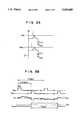
- FIGS. 1A and 1Bare diagrams showing a driving method according to a first embodiment of the present invention
- FIGS. 2A and 2Bare diagrams showing a driving method according to a second embodiment of the present invention.
- FIGS. 3A and 3Bare diagrams showing a driving method according to a third embodiment of the present invention.
- FIGS. 4A and 4Bare diagrams showing a driving method according to a fourth embodiment of the present invention.
- FIGS. 5A and 5Bare diagrams showing a driving method according to a fifth embodiment of the present invention.
- FIGS. 6A and 6Bare diagrams showing a driving method according to a sixth embodiment of the present invention.
- FIG. 7is a diagram showing a liquid crystal display to which the driving method of this invention may apply.
- FIG. 8is a timing chart showing a state where a flicker of 60 Hz is alleviated
- FIG. 9is a timing chart showing a state where a flicker of 30 Hz is alleviated.
- FIGS. 10A and 10Bare diagrams showing a conventional display driving method.
- FIGS. 1A and 1Bshow a driving method according to a first embodiment of the invention.
- a numeral 1denotes a scan electrode which is connected to a gate of a thin film transistor (referred to as TFT) 11 to 22.
- a numeral 2denotes a signal electrode which is connected to a drain of the TFT.
- the source of the TFTis connected to one liquid crystal terminal and each opposite electrode is connected to the other liquid crystal terminal.
- V GK , V GK+1 and V GK+2denote any gate voltage.
- V Ddenotes any drain voltage.
- V comdenotes a voltage applied to the opposite electrode.
- C LC11 , C LC12 and C LC21denote a liquid crystal capacitance (pixel).
- V C1denotes a central voltage of an amplitude of V D .
- V C2denotes a central voltage of an amplitude of V com .
- 1Hdenotes a selecting time (scan time) of one scan line.
- positive-polarity signals V Dare applied to the pixels C LC11 and C LC12 connected to a group of odd scan lines V GK and V KG+2 .
- negative-polarity signals V Dare applied to the pixels C LC21 and C LC22 connected to a group of even scan lines V GK+1 .
- This driving methodis, therefore, arranged so as to invert V D and V com like alternate current at each field. This makes it possible to more easily design both of the voltage-alternating circuits for V D and V com , thereby improving the reliability of an active matrix liquid crystal display to which the driving method applies. Moreover, in the driving method, it is more likely that the flicker appearing in the group of pixels connected to the even scan lines may be offset against the flicker appearing in the group of pixels connected to the odd scan lines. This results in suppressing the flicker on the overall display.
- FIGS. 2A and 2Bshow a driving method according to a second embodiment of the present invention.
- the circuit arrangement of the display of the second embodimentis such that the scan electrode 1 is connected to a gate of each TFT, a signal electrode 2 is connected to a drain of each TFT, one liquid crystal terminal is connected to a source of each TFT, and the other liquid crystal terminal is connected to an opposite electrode.
- V GK and V GK1denote any gate voltage.
- V Ddenotes any drain voltage.
- V comdenotes a voltage applied to the opposite electrode.
- C LCdenotes a liquid crystal capacitance.
- V C1denotes a central voltage of an amplitude of V D .
- V C2denotes a central voltage of an amplitude of V com .
- 1Hdenotes a selecting time of one scan line.
- the driving method of the present embodimentis arranged so that the positive-polarity signal and the negative-polarity signal are applied to the drain electrodes in a manner to shift these signals by 1/2 field within a one-field time interval.
- the use of the driving methodmakes it possible to invert V D and V com like alternate current at each field.
- the driving method of this embodimentcan reduce the driving current to a small value.
- the use of this driving methodmakes it possible to offset the flicker appearing by applying a d.c. voltage into a group of a liquid crystal pixels connected to the even scan lines against the flicker appearing by applying a d.c. voltage into a group of pixels connected to the odd scan lines. This results in reducing the flicker on the overall screen.
- FIGS. 8 and 9show how the flicker is reduced on the overall screen if the driving method of this embodiment is used.
- FIG. 8shows how the flicker of 60 Hz is alleviated
- FIG. 9shows how the flicker of 30 Hz is alleviated.
- the driving method of the second embodimentas shown in FIG. 8
- the flicker appearing to the pixels connected to the K-th scan lineis added to the flicker appearing to the pixels connected to the (K+1)th scan line
- the resulting flickerhas a tabular waveform. This means that the flicker on the overall screen is made smaller.
- the driving method of the second embodimentas shown in FIG.
- the actual flickeris an addition of the flicker appearing in the pixels connected to the k-th scan line to the flicker appearing in the pixels connected to (K+1)th scan line.
- This additive flickerhas only the flicker of 60 Hz with no flicker of 30 Hz. A human cannot visually feel the flicker of 60 Hz. This means that the flicker on the overall screen is reduced.
- FIGS. 3A and 3Bshow a driving method according to a third embodiment of the present invention.
- a gate of a TFTis connected to a scan electrode 1 and a drain of the TFT is connected to a signal electrode 2.
- One liquid crystal terminal and a storage capacitance electrodeare connected to a source of the TFT.
- the other liquid crystal terminal and storage capacitance electrodeare connected to an opposite electrode.
- V GK and V KG+1denote any gate voltage.
- V Ddenotes any drain voltage.
- V comdenotes a voltage applied to the opposite electrode.
- C LCdenotes a liquid crystal capacitance.
- C STGdenotes a storage capacitance.
- V C1denotes a central voltage of an amplitude of V D .
- V C2denotes a central voltage of an amplitude of V com .
- 1Hdenotes a selecting time of one scan line.
- positive-polarity signalsare applied to a group of pixels connected to odd scan lines.
- negative-polarity signalsare applied to the group of pixels connected to even scan lines.
- the negative-polarity signalsare applied to the group of pixels connected to the odd scan lines.
- the positive-polarity signalsare applied to the group of pixels connected to the even scan lines. Later, this process is repeated.
- the driving method of the third embodimentis arranged so that the positive-polarity signals and the negative-polarity signals served as a display signal within one field are applied to a group of drain electrodes in a manner to shift both of the signals by 1/2 field.
- the use of the driving methodmakes it possible to invert V D and V com like alternate current at each field.
- this driving methodmakes it easier to design both of the voltage-alternating circuits for V D and V com and thereby improve the reliability of an active matrix liquid crystal display.
- the use of this driving methodmakes it possible to offset the flicker appearing in a group of a liquid crystal pixels connected to the even scan lines against the flicker appearing in a group of pixels connected to the odd scan lines. This results in reducing the flicker on the overall screen.
- FIGS. 4A and 4Bshow a driving method according to a fourth embodiment of the present invention.
- a scan electrode 1is connected to a gate of a TFT and a signal electrode 2 is connected to a drain of the TFT.
- One liquid crystal terminalis connected to a source of the TFT and the other liquid crystal terminal is connected to an opposite electrode.
- One storage capacitance electrodeis connected to a source of the TFT and the other storage capacitance electrode is connected to a scan electrode at the previous stage.
- V GK-1 V GK and V KG+1denote any gate voltage.
- V Ddenotes any drain voltage.
- V comdenotes a voltage applied to the opposite electrode.
- C LCdenotes a liquid crystal capacitance.
- C STGdenotes a storage capacitance.
- V C1denotes a central voltage of an amplitude of V D .
- V C2denotes a central voltage of an amplitude of V com .
- 1Hdenotes a selecting time of one scan line.
- the other storage capacitance electrodeis connected to the scan electrode at the previous stage.
- the gate voltageneeds to have three stages.
- positive-polarity signalsare applied to the group of pixels connected to odd scan lines.
- negative-polarity signalsare applied to the group of pixels connected to even scan lines.
- positive-polarity signalsare applied to the group of pixels connected to the even scan lines. Then, this process is repeated. That is, the positive-polarity signals and the negative-polarity signals are applied to a group of drain electrodes in such a manner that these signals are shifted by 1/n (n>1) field within one field.
- This driving methodis, therefore, arranged so as to invert V D and V com like alternate current at each one field. This makes it possible to more easily design both of the voltage-alternating circuits for V D and V com , thereby improving the reliability of an active matrix liquid crystal display to which the driving method applies. Moreover, in the driving method, it is more likely that the flicker appearing in the group of pixels connected to the even scan lines may be offset against the flicker appearing in the group of pixels connected to the odd scan lines. This results in reducing the flicker on the overall display.
- amorphous silicon TFTsince the amorphous silicon TFT has a low current feeding capability, in actuality, it is quite difficult to actuate a high-definition display consisting of 1024 scan lines to keep the display at high quality.
- a positive-polarity drain signalmay not be sufficiently applied to the liquid crystal display terminal through the amorphous silicon TFT (a-Si TFT). This is because the voltage V GS between the gate and the source when the TFT is active is made lower according to the rise of an electric potential at the liquid crystal terminal and the on-resistance of each TFT is made higher accordingly.
- V GSis kept constant without having any relation with lowering of an electric potential at the liquid crystal terminal.
- the on-resistance of each TFTis quite low. This means that when the drain signal is at negative polarity, the drain signal is allowed to be applied to the liquid crystal terminal at a relatively fast speed.
- FIGS. 5A and 5Bshow a driving method according to a fifth embodiment of the present invention.
- a scan electrode 1is connected to a gate of a TFT and a signal electrode 2 is connected to a drain of the TFT.
- One liquid crystal terminal and storage capacitance electrodeare connected to a source of the TFT and the other liquid crystal terminal and storage capacitance electrode are connected to an opposite electrode.
- V GK and V GK+1denote any gate voltage.
- V Ddenotes any drain voltage.
- V comdenotes a voltage applied to the opposite electrode.
- C LCdenotes a liquid crystal capacitance.
- C STGdenotes a storage capacitance.
- V C1denotes a central voltage of an amplitude of V D .
- V C2denotes a central voltage of an amplitude of V com .
- 1H(+)denotes a gate pulse width provided when a positive-polarity signal is applied.
- 1H(-)denotes a gate pulse width provided when a negative-polarity signal is applied.
- the use of the driving method shown in FIGS. 5A and 5Bmake the gate pulse width at the positive-polarity drain signal longer than the gate pulse width at the negative-polarity drain signal.
- the a-Si TFThas a low driving capability when a positive-polarity signal is applied, since the gate pulse width is longer, a sufficient drain signal is allowed to be applied to the liquid crystal terminal.
- the driving method of the fifth embodimentallows a high-definition display consisting of about 1024 scan lines to have an excellent display quality.
- FIGS. 6A and 6Bshow a driving method according to a sixth embodiment of the present invention.
- One of the pixels included in a display unitis arranged so that a scan electrode 1 is connected to a gate of a TFT and a signal electrode is connected to a drain of the TFT.
- One liquid crystal terminalis connected to a source of the TFT and the other liquid crystal terminal is connected to an opposite electrode.
- One storage capacitance electrodeis connected to the source of the TFT and the other storage capacitance electrode is connected to a scan electrode at the previous stage.
- V GK-1 , V GK and V GK+1denote any gate signal.
- V Ddenotes any drain voltage.
- V comdenotes a voltage applied to the opposite electrode.
- C LCdenotes a liquid crystal capacitance.
- C STGdenotes a storage capacitance.
- V C1denotes a central voltage of an amplitude of V D .
- V C2denotes a central voltage of an amplitude of Vcom.
- 1H(+)denotes a gate pulse width provided when a positive-polarity signal is applied.
- 1H(-)denotes a gate pulse width provided when a negative-polarity signal is applied.
- the driving method of this embodimentmakes the gate pulse width given when the drain signal is at positive polarity longer than that given when the drain signal is at negative polarity.
- the a-Si TFThas a low driving capability when it is at positive polarity. Since, however, the gate pulse width is longer, the drain signal is sufficiently applied to the liquid crystal terminal.
- the driving method of this embodimentallows a high-definition display consisting of about 1024 lines to have an excellent display quality.
- FIG. 7shows a thin film transistor liquid crystal display (referred to as a TFT-LCD).
- TFT-LCDthin film transistor liquid crystal display
Landscapes
- Engineering & Computer Science (AREA)
- Chemical & Material Sciences (AREA)
- Crystallography & Structural Chemistry (AREA)
- Physics & Mathematics (AREA)
- Computer Hardware Design (AREA)
- General Physics & Mathematics (AREA)
- Theoretical Computer Science (AREA)
- Power Engineering (AREA)
- Liquid Crystal Display Device Control (AREA)
- Liquid Crystal (AREA)
Abstract
Description
Claims (18)
Priority Applications (1)
| Application Number | Priority Date | Filing Date | Title |
|---|---|---|---|
| US08/328,547US5430460A (en) | 1991-09-17 | 1994-10-25 | Method and apparatus for driving liquid crystal display unit |
Applications Claiming Priority (4)
| Application Number | Priority Date | Filing Date | Title |
|---|---|---|---|
| JP3-235928 | 1991-09-17 | ||
| JP3235928AJPH0572999A (en) | 1991-09-17 | 1991-09-17 | Liquid crystal display device and its driving method |
| US94593592A | 1992-09-17 | 1992-09-17 | |
| US08/328,547US5430460A (en) | 1991-09-17 | 1994-10-25 | Method and apparatus for driving liquid crystal display unit |
Related Parent Applications (1)
| Application Number | Title | Priority Date | Filing Date |
|---|---|---|---|
| US94593592AContinuation | 1991-09-17 | 1992-09-17 |
Publications (1)
| Publication Number | Publication Date |
|---|---|
| US5430460Atrue US5430460A (en) | 1995-07-04 |
Family
ID=16993317
Family Applications (1)
| Application Number | Title | Priority Date | Filing Date |
|---|---|---|---|
| US08/328,547Expired - LifetimeUS5430460A (en) | 1991-09-17 | 1994-10-25 | Method and apparatus for driving liquid crystal display unit |
Country Status (3)
| Country | Link |
|---|---|
| US (1) | US5430460A (en) |
| JP (1) | JPH0572999A (en) |
| KR (1) | KR100241035B1 (en) |
Cited By (21)
| Publication number | Priority date | Publication date | Assignee | Title |
|---|---|---|---|---|
| EP0764932A3 (en)* | 1995-09-07 | 1997-05-02 | Samsung Electronics Co Ltd | |
| US5818402A (en)* | 1996-01-19 | 1998-10-06 | Lg Electronics Inc. | Display driver for reducing crosstalk by detecting current at the common electrode and applying a compensation voltage to the common electrode |
| US5945970A (en)* | 1996-09-06 | 1999-08-31 | Samsung Electronics Co., Ltd. | Liquid crystal display devices having improved screen clearing capability and methods of operating same |
| US5977940A (en)* | 1996-03-07 | 1999-11-02 | Kabushiki Kaisha Toshiba | Liquid crystal display device |
| US6046716A (en) | 1996-12-19 | 2000-04-04 | Colorado Microdisplay, Inc. | Display system having electrode modulation to alter a state of an electro-optic layer |
| US6057820A (en)* | 1996-10-21 | 2000-05-02 | Spatialight, Inc. | Apparatus and method for controlling contrast in a dot-matrix liquid crystal display |
| US6166714A (en)* | 1996-06-06 | 2000-12-26 | Kabushiki Kaisha Toshiba | Displaying device |
| US6243064B1 (en)* | 1995-11-07 | 2001-06-05 | Semiconductor Energy Laboratory Co., Ltd. | Active matrix type liquid-crystal display unit and method of driving the same |
| US6621102B2 (en) | 1995-11-04 | 2003-09-16 | Semiconductor Energy Laboratory Co., Ltd. | Electro-optical device |
| EP1349141A1 (en)* | 2002-03-28 | 2003-10-01 | Seiko Epson Corporation | Capacitor discharging method for preventing afterimages in an active matrix liquid crystal display |
| US20040066362A1 (en)* | 2001-05-04 | 2004-04-08 | Feng-Ting Pai | Active matrix display and driving method thereof |
| US20040095308A1 (en)* | 2002-02-10 | 2004-05-20 | Samsung Electronics Co., Ltd. | Liquid crystal display |
| US20040108987A1 (en)* | 2002-12-04 | 2004-06-10 | Lg.Philips Lcd Co., Ltd. | System and method for reducing off-current in thin film transistor of liquid crystal display device |
| US20050041006A1 (en)* | 2003-08-21 | 2005-02-24 | Lee Jae Kyun | Liquid crystal display apparatus and driving method thereof |
| US20050083319A1 (en)* | 2003-10-15 | 2005-04-21 | International Business Machines Corporation | Image display device, pixel drive method, and scan line drive circuit |
| US6906692B2 (en)* | 2000-03-28 | 2005-06-14 | Seiko Epson Corporation | Liquid crystal device, liquid crystal driving device and method of driving the same and electronic equipment |
| US20050225545A1 (en)* | 1998-02-24 | 2005-10-13 | Nec Corporation | Liquid crystal display apparatus and method of driving the same |
| US7196683B2 (en)* | 2000-04-10 | 2007-03-27 | Sharp Kabushiki Kaisha | Driving method of image display device, driving device of image display device, and image display device |
| US20120038692A1 (en)* | 2010-08-11 | 2012-02-16 | Seiko Epson Corporation | Electro-optic device and electronic apparatus |
| US20140240301A1 (en)* | 2012-01-25 | 2014-08-28 | Sharp Kabushiki Kaisha | Liquid crystal display device and drive method thereof |
| CN104571718A (en)* | 2015-01-09 | 2015-04-29 | 友达光电股份有限公司 | Touch panel and detection method thereof |
Families Citing this family (4)
| Publication number | Priority date | Publication date | Assignee | Title |
|---|---|---|---|---|
| JP4801848B2 (en)* | 2001-06-22 | 2011-10-26 | 東芝モバイルディスプレイ株式会社 | Liquid crystal display |
| US20070013631A1 (en)* | 2005-07-13 | 2007-01-18 | Au Optronics Corporation | Liquid crystal display driving methodology with improved power consumption |
| CN105390102B (en)* | 2015-11-02 | 2017-10-17 | 武汉华星光电技术有限公司 | The display device of gate driving circuit and the application circuit |
| CN108694922B (en)* | 2018-04-03 | 2020-11-03 | 昆山龙腾光电股份有限公司 | Common voltage driving method and device and display device |
Citations (4)
| Publication number | Priority date | Publication date | Assignee | Title |
|---|---|---|---|---|
| US4591848A (en)* | 1982-04-01 | 1986-05-27 | Seiko Epson Corporation | Matrix panel with an active driving system |
| US4734692A (en)* | 1985-04-26 | 1988-03-29 | Matsushita Electric Industrial Co., Ltd. | Driver circuit for liquid crystal display |
| US4870399A (en)* | 1987-08-24 | 1989-09-26 | North American Philips Corporation | Apparatus for addressing active displays |
| US4922240A (en)* | 1987-12-29 | 1990-05-01 | North American Philips Corp. | Thin film active matrix and addressing circuitry therefor |
- 1991
- 1991-09-17JPJP3235928Apatent/JPH0572999A/enactivePending
- 1992
- 1992-09-17KRKR1019920016915Apatent/KR100241035B1/ennot_activeExpired - Fee Related
- 1994
- 1994-10-25USUS08/328,547patent/US5430460A/ennot_activeExpired - Lifetime
Patent Citations (4)
| Publication number | Priority date | Publication date | Assignee | Title |
|---|---|---|---|---|
| US4591848A (en)* | 1982-04-01 | 1986-05-27 | Seiko Epson Corporation | Matrix panel with an active driving system |
| US4734692A (en)* | 1985-04-26 | 1988-03-29 | Matsushita Electric Industrial Co., Ltd. | Driver circuit for liquid crystal display |
| US4870399A (en)* | 1987-08-24 | 1989-09-26 | North American Philips Corporation | Apparatus for addressing active displays |
| US4922240A (en)* | 1987-12-29 | 1990-05-01 | North American Philips Corp. | Thin film active matrix and addressing circuitry therefor |
Cited By (39)
| Publication number | Priority date | Publication date | Assignee | Title |
|---|---|---|---|---|
| US5793346A (en)* | 1995-09-07 | 1998-08-11 | Samsung Electronics Co., Ltd. | Liquid crystal display devices having active screen clearing circuits therein |
| EP0764932A3 (en)* | 1995-09-07 | 1997-05-02 | Samsung Electronics Co Ltd | |
| US6621102B2 (en) | 1995-11-04 | 2003-09-16 | Semiconductor Energy Laboratory Co., Ltd. | Electro-optical device |
| US6456269B2 (en)* | 1995-11-07 | 2002-09-24 | Semiconductor Energy Laboratory Co., Ltd. | Active matrix type liquid-crystal display unit and method of driving the same |
| US6243064B1 (en)* | 1995-11-07 | 2001-06-05 | Semiconductor Energy Laboratory Co., Ltd. | Active matrix type liquid-crystal display unit and method of driving the same |
| US5818402A (en)* | 1996-01-19 | 1998-10-06 | Lg Electronics Inc. | Display driver for reducing crosstalk by detecting current at the common electrode and applying a compensation voltage to the common electrode |
| US5977940A (en)* | 1996-03-07 | 1999-11-02 | Kabushiki Kaisha Toshiba | Liquid crystal display device |
| US6166714A (en)* | 1996-06-06 | 2000-12-26 | Kabushiki Kaisha Toshiba | Displaying device |
| US5945970A (en)* | 1996-09-06 | 1999-08-31 | Samsung Electronics Co., Ltd. | Liquid crystal display devices having improved screen clearing capability and methods of operating same |
| US6057820A (en)* | 1996-10-21 | 2000-05-02 | Spatialight, Inc. | Apparatus and method for controlling contrast in a dot-matrix liquid crystal display |
| US6329971B2 (en)* | 1996-12-19 | 2001-12-11 | Zight Corporation | Display system having electrode modulation to alter a state of an electro-optic layer |
| US6046716A (en) | 1996-12-19 | 2000-04-04 | Colorado Microdisplay, Inc. | Display system having electrode modulation to alter a state of an electro-optic layer |
| US7652648B2 (en) | 1998-02-24 | 2010-01-26 | Nec Corporation | Liquid crystal display apparatus and method of driving the same |
| US7161573B1 (en)* | 1998-02-24 | 2007-01-09 | Nec Corporation | Liquid crystal display unit and method for driving the same |
| US20050225545A1 (en)* | 1998-02-24 | 2005-10-13 | Nec Corporation | Liquid crystal display apparatus and method of driving the same |
| US7268761B2 (en) | 2000-03-28 | 2007-09-11 | Seiko Epson Corporation | Liquid crystal device, liquid crystal driving device and method of driving the same, and electronic equipment |
| US20070279406A1 (en)* | 2000-03-28 | 2007-12-06 | Seiko Epson Corporation | Liquid Crystal Device, Liquid Crystal Driving Device and Method of Driving the Same and Electronic Equipment |
| US6906692B2 (en)* | 2000-03-28 | 2005-06-14 | Seiko Epson Corporation | Liquid crystal device, liquid crystal driving device and method of driving the same and electronic equipment |
| US20050212745A1 (en)* | 2000-03-28 | 2005-09-29 | Seiko Epson Corporation | Liquid crystal device, liquid crystal driving device and method of driving the same, and electronic equipment |
| US7196683B2 (en)* | 2000-04-10 | 2007-03-27 | Sharp Kabushiki Kaisha | Driving method of image display device, driving device of image display device, and image display device |
| US20040066362A1 (en)* | 2001-05-04 | 2004-04-08 | Feng-Ting Pai | Active matrix display and driving method thereof |
| US6999054B2 (en)* | 2001-05-04 | 2006-02-14 | Hannstar Display Corp. | Active matrix display and driving method thereof |
| US20040095308A1 (en)* | 2002-02-10 | 2004-05-20 | Samsung Electronics Co., Ltd. | Liquid crystal display |
| US20030218593A1 (en)* | 2002-03-28 | 2003-11-27 | Seiko Epson Corporation | Electrooptic device, driving method therefor, electronic device, and projection display device |
| US7098880B2 (en) | 2002-03-28 | 2006-08-29 | Seiko Epson Corporation | Electrooptic device, driving method therefor, electronic device, and projection display device |
| EP1349141A1 (en)* | 2002-03-28 | 2003-10-01 | Seiko Epson Corporation | Capacitor discharging method for preventing afterimages in an active matrix liquid crystal display |
| US7193599B2 (en)* | 2002-10-02 | 2007-03-20 | Samsung Electronics Co, Ltd. | Liquid crystal display |
| US7123230B2 (en)* | 2002-12-04 | 2006-10-17 | Lg.Philips Lcd Co., Ltd. | System and method for reducing off-current in thin film transistor of liquid crystal display device |
| US20040108987A1 (en)* | 2002-12-04 | 2004-06-10 | Lg.Philips Lcd Co., Ltd. | System and method for reducing off-current in thin film transistor of liquid crystal display device |
| US20050041006A1 (en)* | 2003-08-21 | 2005-02-24 | Lee Jae Kyun | Liquid crystal display apparatus and driving method thereof |
| US7425942B2 (en)* | 2003-08-21 | 2008-09-16 | Lg Display Co., Ltd. | Liquid crystal display apparatus and driving method thereof |
| US7173600B2 (en)* | 2003-10-15 | 2007-02-06 | International Business Machines Corporation | Image display device, pixel drive method, and scan line drive circuit |
| US20050083319A1 (en)* | 2003-10-15 | 2005-04-21 | International Business Machines Corporation | Image display device, pixel drive method, and scan line drive circuit |
| US20120038692A1 (en)* | 2010-08-11 | 2012-02-16 | Seiko Epson Corporation | Electro-optic device and electronic apparatus |
| US9111496B2 (en)* | 2010-08-11 | 2015-08-18 | Seiko Epson Corporation | Electro-optic device and electronic apparatus with a control signal including a precharge period |
| US20140240301A1 (en)* | 2012-01-25 | 2014-08-28 | Sharp Kabushiki Kaisha | Liquid crystal display device and drive method thereof |
| US9305507B2 (en)* | 2012-01-25 | 2016-04-05 | Sharp Kabushiki Kaisha | Liquid crystal display device capable of performing 2D display and 3D display, and drive method thereof |
| CN104571718A (en)* | 2015-01-09 | 2015-04-29 | 友达光电股份有限公司 | Touch panel and detection method thereof |
| CN104571718B (en)* | 2015-01-09 | 2017-07-28 | 友达光电股份有限公司 | Touch panel and detection method thereof |
Also Published As
| Publication number | Publication date |
|---|---|
| JPH0572999A (en) | 1993-03-26 |
| KR100241035B1 (en) | 2000-02-01 |
Similar Documents
| Publication | Publication Date | Title |
|---|---|---|
| US5430460A (en) | Method and apparatus for driving liquid crystal display unit | |
| JP2937130B2 (en) | Active matrix type liquid crystal display | |
| US4804951A (en) | Display apparatus and driving method therefor | |
| US5648793A (en) | Driving system for active matrix liquid crystal display | |
| KR100272873B1 (en) | Active-matrix display system with less signal line drive circuits | |
| CA2046357C (en) | Liquid crystal display | |
| US6396468B2 (en) | Liquid crystal display device | |
| KR100561946B1 (en) | LCD and its driving method | |
| EP0436384B1 (en) | A driving circuit for a liquid crystal display apparatus | |
| KR100350726B1 (en) | Method Of Driving Gates of LCD | |
| US5654733A (en) | Liquid crystal electrooptical device | |
| US10896650B2 (en) | Video signal line drive circuit, display device including same, and drive method for video signal line | |
| JPH09171168A (en) | Scan line pair non-overlapping scanning method for liquid crystal display device | |
| JPH07199154A (en) | Liquid crystal display | |
| KR20030033050A (en) | Display devices and driving method therefor | |
| JP4902185B2 (en) | Display device | |
| JPH04309920A (en) | Driving method for liquid crystal display device | |
| JP3376088B2 (en) | Active matrix liquid crystal display device and driving method thereof | |
| KR100853215B1 (en) | Liquid crystal display | |
| JPS6126074B2 (en) | ||
| JPH0244189B2 (en) | ||
| JPH02196218A (en) | Driving method for liquid crystal display device | |
| US5241392A (en) | Liquid crystal display | |
| JP3666920B2 (en) | Active matrix liquid crystal display | |
| JPH09211423A (en) | Driving method of active matrix liquid crystal display |
Legal Events
| Date | Code | Title | Description |
|---|---|---|---|
| STCF | Information on status: patent grant | Free format text:PATENTED CASE | |
| FPAY | Fee payment | Year of fee payment:4 | |
| FEPP | Fee payment procedure | Free format text:PAYOR NUMBER ASSIGNED (ORIGINAL EVENT CODE: ASPN); ENTITY STATUS OF PATENT OWNER: LARGE ENTITY | |
| FPAY | Fee payment | Year of fee payment:8 | |
| FPAY | Fee payment | Year of fee payment:12 | |
| AS | Assignment | Owner name:PANASONIC LIQUID CRYSTAL DISPLAY CO., LTD., JAPAN Free format text:MERGER/CHANGE OF NAME;ASSIGNOR:IPS ALPHA SUPPORT CO., LTD.;REEL/FRAME:027363/0315 Effective date:20101001 Owner name:IPS ALPHA SUPPORT CO., LTD., JAPAN Free format text:COMPANY SPLIT PLAN TRANSFERRING FIFTY (50) PERCENT SHARE OF PATENTS AND PATENT APPLICATIONS;ASSIGNOR:HITACHI DISPLAYS, LTD.;REEL/FRAME:027362/0466 Effective date:20100630 Owner name:HITACHI DISPLAYS, LTD., JAPAN Free format text:COMPANY SPLIT PLAN TRANSFERRING ONE HUNDRED (100) PERCENT SHARE OF PATENT AND PATENT APPLICATIONS;ASSIGNOR:HITACHI, LTD.;REEL/FRAME:027362/0612 Effective date:20021001 |