US5429070A - High density plasma deposition and etching apparatus - Google Patents
High density plasma deposition and etching apparatusDownload PDFInfo
- Publication number
- US5429070A US5429070AUS07/979,574US97957492AUS5429070AUS 5429070 AUS5429070 AUS 5429070AUS 97957492 AUS97957492 AUS 97957492AUS 5429070 AUS5429070 AUS 5429070A
- Authority
- US
- United States
- Prior art keywords
- sub
- plasma
- substrate
- etching
- magnetic field
- Prior art date
- Legal status (The legal status is an assumption and is not a legal conclusion. Google has not performed a legal analysis and makes no representation as to the accuracy of the status listed.)
- Expired - Lifetime
Links
- 238000005530etchingMethods0.000titleabstractdescription84
- 230000008021depositionEffects0.000titleabstractdescription47
- 239000000758substrateSubstances0.000claimsabstractdescription129
- 238000000034methodMethods0.000claimsabstractdescription98
- 230000008569processEffects0.000claimsabstractdescription84
- 239000004020conductorSubstances0.000claimsabstractdescription15
- 238000012545processingMethods0.000claimsabstractdescription12
- 229910052731fluorineInorganic materials0.000claimsabstractdescription11
- 239000011737fluorineSubstances0.000claimsabstractdescription11
- PNEYBMLMFCGWSK-UHFFFAOYSA-Naluminium oxideInorganic materials[O-2].[O-2].[O-2].[Al+3].[Al+3]PNEYBMLMFCGWSK-UHFFFAOYSA-N0.000claimsabstractdescription8
- 229910052594sapphireInorganic materials0.000claimsabstractdescription7
- 239000010980sapphireSubstances0.000claimsabstractdescription7
- PXGOKWXKJXAPGV-UHFFFAOYSA-NFluorineChemical compoundFFPXGOKWXKJXAPGV-UHFFFAOYSA-N0.000claimsabstract3
- 239000007789gasSubstances0.000claimsdescription100
- VYPSYNLAJGMNEJ-UHFFFAOYSA-Nsilicon dioxideInorganic materialsO=[Si]=OVYPSYNLAJGMNEJ-UHFFFAOYSA-N0.000claimsdescription29
- 239000010453quartzSubstances0.000claimsdescription21
- 229910052782aluminiumInorganic materials0.000claimsdescription17
- XAGFODPZIPBFFR-UHFFFAOYSA-NaluminiumChemical compound[Al]XAGFODPZIPBFFR-UHFFFAOYSA-N0.000claimsdescription17
- 229910021420polycrystalline siliconInorganic materials0.000claimsdescription17
- 229920005591polysiliconPolymers0.000claimsdescription13
- 229910052751metalInorganic materials0.000claimsdescription11
- 239000002184metalSubstances0.000claimsdescription11
- 150000002736metal compoundsChemical class0.000claimsdescription2
- 210000002381plasmaAnatomy0.000abstractdescription232
- 239000010432diamondSubstances0.000abstractdescription3
- 229910003460diamondInorganic materials0.000abstractdescription3
- 239000000460chlorineSubstances0.000description62
- 238000000151depositionMethods0.000description48
- 235000012431wafersNutrition0.000description29
- 235000012239silicon dioxideNutrition0.000description23
- 238000013016dampingMethods0.000description20
- 229910052786argonInorganic materials0.000description19
- 229910052734heliumInorganic materials0.000description19
- 239000010408filmSubstances0.000description17
- 239000000463materialSubstances0.000description17
- 241001364096PachycephalidaeSpecies0.000description16
- 150000002500ionsChemical class0.000description15
- KZBUYRJDOAKODT-UHFFFAOYSA-NChlorineChemical compoundClClKZBUYRJDOAKODT-UHFFFAOYSA-N0.000description12
- 239000006185dispersionSubstances0.000description10
- 229920002120photoresistant polymerPolymers0.000description10
- 238000001020plasma etchingMethods0.000description10
- 230000007246mechanismEffects0.000description9
- 239000000203mixtureSubstances0.000description9
- 229910052760oxygenInorganic materials0.000description9
- 238000004544sputter depositionMethods0.000description9
- XKRFYHLGVUSROY-UHFFFAOYSA-NArgonChemical compound[Ar]XKRFYHLGVUSROY-UHFFFAOYSA-N0.000description8
- YCKRFDGAMUMZLT-UHFFFAOYSA-NFluorine atomChemical compound[F]YCKRFDGAMUMZLT-UHFFFAOYSA-N0.000description8
- 239000010949copperSubstances0.000description8
- 230000008878couplingEffects0.000description8
- 238000010168coupling processMethods0.000description8
- 238000005859coupling reactionMethods0.000description8
- 238000010586diagramMethods0.000description8
- 230000005684electric fieldEffects0.000description8
- 230000005284excitationEffects0.000description8
- 229910001220stainless steelInorganic materials0.000description8
- 239000010935stainless steelSubstances0.000description8
- 238000000576coating methodMethods0.000description7
- 230000004907fluxEffects0.000description7
- FAQYAMRNWDIXMY-UHFFFAOYSA-NtrichloroboraneChemical compoundClB(Cl)ClFAQYAMRNWDIXMY-UHFFFAOYSA-N0.000description7
- BSYNRYMUTXBXSQ-UHFFFAOYSA-NAspirinChemical compoundCC(=O)OC1=CC=CC=C1C(O)=OBSYNRYMUTXBXSQ-UHFFFAOYSA-N0.000description6
- ZAMOUSCENKQFHK-UHFFFAOYSA-NChlorine atomChemical compound[Cl]ZAMOUSCENKQFHK-UHFFFAOYSA-N0.000description6
- RYGMFSIKBFXOCR-UHFFFAOYSA-NCopperChemical compound[Cu]RYGMFSIKBFXOCR-UHFFFAOYSA-N0.000description6
- 229910052801chlorineInorganic materials0.000description6
- 238000001816coolingMethods0.000description6
- 229910052802copperInorganic materials0.000description6
- 238000002347injectionMethods0.000description6
- 239000007924injectionSubstances0.000description6
- WFKWXMTUELFFGS-UHFFFAOYSA-NtungstenChemical compound[W]WFKWXMTUELFFGS-UHFFFAOYSA-N0.000description6
- RZVAJINKPMORJF-UHFFFAOYSA-NAcetaminophenChemical compoundCC(=O)NC1=CC=C(O)C=C1RZVAJINKPMORJF-UHFFFAOYSA-N0.000description5
- 125000004429atomChemical group0.000description5
- QVGXLLKOCUKJST-UHFFFAOYSA-Natomic oxygenChemical compound[O]QVGXLLKOCUKJST-UHFFFAOYSA-N0.000description5
- 239000011248coating agentSubstances0.000description5
- 238000004519manufacturing processMethods0.000description5
- 239000001301oxygenSubstances0.000description5
- 239000002245particleSubstances0.000description5
- 239000005297pyrexSubstances0.000description5
- 238000001228spectrumMethods0.000description5
- 230000032258transportEffects0.000description5
- 229910052721tungstenInorganic materials0.000description5
- 239000010937tungstenSubstances0.000description5
- 238000013459approachMethods0.000description4
- 238000005229chemical vapour depositionMethods0.000description4
- 238000010438heat treatmentMethods0.000description4
- 230000003993interactionEffects0.000description4
- 150000002739metalsChemical class0.000description4
- 239000000377silicon dioxideSubstances0.000description4
- 239000003990capacitorSubstances0.000description3
- 239000000498cooling waterSubstances0.000description3
- 230000007423decreaseEffects0.000description3
- 230000003247decreasing effectEffects0.000description3
- 238000013461designMethods0.000description3
- 229910052750molybdenumInorganic materials0.000description3
- 229910052757nitrogenInorganic materials0.000description3
- 239000010936titaniumSubstances0.000description3
- 239000013598vectorSubstances0.000description3
- IJGRMHOSHXDMSA-UHFFFAOYSA-NAtomic nitrogenChemical compoundN#NIJGRMHOSHXDMSA-UHFFFAOYSA-N0.000description2
- 229910015844BCl3Inorganic materials0.000description2
- XPDWGBQVDMORPB-UHFFFAOYSA-NFluoroformChemical compoundFC(F)FXPDWGBQVDMORPB-UHFFFAOYSA-N0.000description2
- 229910015325MoFeInorganic materials0.000description2
- ZOKXTWBITQBERF-UHFFFAOYSA-NMolybdenumChemical compound[Mo]ZOKXTWBITQBERF-UHFFFAOYSA-N0.000description2
- 108010038629MolybdoferredoxinProteins0.000description2
- 239000004642PolyimideSubstances0.000description2
- NRTOMJZYCJJWKI-UHFFFAOYSA-NTitanium nitrideChemical compound[Ti]#NNRTOMJZYCJJWKI-UHFFFAOYSA-N0.000description2
- 230000015572biosynthetic processEffects0.000description2
- 239000000919ceramicSubstances0.000description2
- 238000006243chemical reactionMethods0.000description2
- 230000001419dependent effectEffects0.000description2
- 238000009795derivationMethods0.000description2
- 238000009826distributionMethods0.000description2
- 230000000694effectsEffects0.000description2
- 239000011521glassSubstances0.000description2
- 239000001307heliumSubstances0.000description2
- SWQJXJOGLNCZEY-UHFFFAOYSA-Nhelium atomChemical compound[He]SWQJXJOGLNCZEY-UHFFFAOYSA-N0.000description2
- 229910052739hydrogenInorganic materials0.000description2
- 230000006698inductionEffects0.000description2
- VNWKTOKETHGBQD-UHFFFAOYSA-NmethaneChemical compoundCVNWKTOKETHGBQD-UHFFFAOYSA-N0.000description2
- 239000011733molybdenumSubstances0.000description2
- 150000004767nitridesChemical class0.000description2
- 238000000623plasma-assisted chemical vapour depositionMethods0.000description2
- 229920001721polyimidePolymers0.000description2
- 238000001878scanning electron micrographMethods0.000description2
- 239000004065semiconductorSubstances0.000description2
- 125000006850spacer groupChemical group0.000description2
- VXUYXOFXAQZZMF-UHFFFAOYSA-Ntitanium(IV) isopropoxideChemical compoundCC(C)O[Ti](OC(C)C)(OC(C)C)OC(C)CVXUYXOFXAQZZMF-UHFFFAOYSA-N0.000description2
- 238000012935AveragingMethods0.000description1
- 229910052582BNInorganic materials0.000description1
- PZNSFCLAULLKQX-UHFFFAOYSA-NBoron nitrideChemical compoundN#BPZNSFCLAULLKQX-UHFFFAOYSA-N0.000description1
- OKTJSMMVPCPJKN-UHFFFAOYSA-NCarbonChemical compound[C]OKTJSMMVPCPJKN-UHFFFAOYSA-N0.000description1
- CPELXLSAUQHCOX-UHFFFAOYSA-NHydrogen bromideChemical compoundBrCPELXLSAUQHCOX-UHFFFAOYSA-N0.000description1
- 229910016006MoSiInorganic materials0.000description1
- 229910018503SF6Inorganic materials0.000description1
- 229910052581Si3N4Inorganic materials0.000description1
- 229910003691SiBrInorganic materials0.000description1
- 229910008484TiSiInorganic materials0.000description1
- RTAQQCXQSZGOHL-UHFFFAOYSA-NTitaniumChemical compound[Ti]RTAQQCXQSZGOHL-UHFFFAOYSA-N0.000description1
- 230000004913activationEffects0.000description1
- AZDRQVAHHNSJOQ-UHFFFAOYSA-NalumaneChemical group[AlH3]AZDRQVAHHNSJOQ-UHFFFAOYSA-N0.000description1
- 229910021417amorphous siliconInorganic materials0.000description1
- 238000004458analytical methodMethods0.000description1
- 230000004888barrier functionEffects0.000description1
- 230000008901benefitEffects0.000description1
- 239000005380borophosphosilicate glassSubstances0.000description1
- -1but not limited toChemical class0.000description1
- 229910052799carbonInorganic materials0.000description1
- 238000003486chemical etchingMethods0.000description1
- 238000004140cleaningMethods0.000description1
- 238000010276constructionMethods0.000description1
- 230000001627detrimental effectEffects0.000description1
- 238000010494dissociation reactionMethods0.000description1
- 230000005593dissociationsEffects0.000description1
- 238000005516engineering processMethods0.000description1
- 230000002708enhancing effectEffects0.000description1
- 230000003628erosive effectEffects0.000description1
- 150000002222fluorine compoundsChemical class0.000description1
- 125000001153fluoro groupChemical groupF*0.000description1
- 230000004927fusionEffects0.000description1
- 150000008282halocarbonsChemical class0.000description1
- 229910052736halogenInorganic materials0.000description1
- 150000002367halogensChemical class0.000description1
- 230000003116impacting effectEffects0.000description1
- 230000001939inductive effectEffects0.000description1
- 238000009616inductively coupled plasmaMethods0.000description1
- 239000011810insulating materialSubstances0.000description1
- 238000004518low pressure chemical vapour depositionMethods0.000description1
- 230000005426magnetic field effectEffects0.000description1
- 238000004377microelectronicMethods0.000description1
- 238000001000micrographMethods0.000description1
- 238000012986modificationMethods0.000description1
- 230000004048modificationEffects0.000description1
- 230000007935neutral effectEffects0.000description1
- 229910052756noble gasInorganic materials0.000description1
- 230000003287optical effectEffects0.000description1
- 238000012856packingMethods0.000description1
- 238000002161passivationMethods0.000description1
- 230000002093peripheral effectEffects0.000description1
- 229920000642polymerPolymers0.000description1
- 230000005855radiationEffects0.000description1
- 238000005546reactive sputteringMethods0.000description1
- LMHHRCOWPQNFTF-UHFFFAOYSA-Ns-propan-2-yl azepane-1-carbothioateChemical compoundCC(C)SC(=O)N1CCCCCC1LMHHRCOWPQNFTF-UHFFFAOYSA-N0.000description1
- 239000000523sampleSubstances0.000description1
- 230000009834selective interactionEffects0.000description1
- 230000035945sensitivityEffects0.000description1
- 238000000926separation methodMethods0.000description1
- 239000005368silicate glassSubstances0.000description1
- 229910021332silicideInorganic materials0.000description1
- 229910052710siliconInorganic materials0.000description1
- HQVNEWCFYHHQES-UHFFFAOYSA-Nsilicon nitrideChemical compoundN12[Si]34N5[Si]62N3[Si]51N64HQVNEWCFYHHQES-UHFFFAOYSA-N0.000description1
- 229910052814silicon oxideInorganic materials0.000description1
- 238000000992sputter etchingMethods0.000description1
- 239000000126substanceSubstances0.000description1
- 229910052717sulfurInorganic materials0.000description1
- SFZCNBIFKDRMGX-UHFFFAOYSA-Nsulfur hexafluorideChemical compoundFS(F)(F)(F)(F)FSFZCNBIFKDRMGX-UHFFFAOYSA-N0.000description1
- 230000002459sustained effectEffects0.000description1
- 239000013077target materialSubstances0.000description1
- 239000010409thin filmSubstances0.000description1
- 229910052719titaniumInorganic materials0.000description1
- MAKDTFFYCIMFQP-UHFFFAOYSA-Ntitanium tungstenChemical compound[Ti].[W]MAKDTFFYCIMFQP-UHFFFAOYSA-N0.000description1
- 238000012546transferMethods0.000description1
- 230000007704transitionEffects0.000description1
- XLYOFNOQVPJJNP-UHFFFAOYSA-NwaterSubstancesOXLYOFNOQVPJJNP-UHFFFAOYSA-N0.000description1
Images


Classifications
- H—ELECTRICITY
- H01—ELECTRIC ELEMENTS
- H01J—ELECTRIC DISCHARGE TUBES OR DISCHARGE LAMPS
- H01J37/00—Discharge tubes with provision for introducing objects or material to be exposed to the discharge, e.g. for the purpose of examination or processing thereof
- H01J37/32—Gas-filled discharge tubes
- H01J37/32431—Constructional details of the reactor
- H01J37/3244—Gas supply means
- C—CHEMISTRY; METALLURGY
- C23—COATING METALLIC MATERIAL; COATING MATERIAL WITH METALLIC MATERIAL; CHEMICAL SURFACE TREATMENT; DIFFUSION TREATMENT OF METALLIC MATERIAL; COATING BY VACUUM EVAPORATION, BY SPUTTERING, BY ION IMPLANTATION OR BY CHEMICAL VAPOUR DEPOSITION, IN GENERAL; INHIBITING CORROSION OF METALLIC MATERIAL OR INCRUSTATION IN GENERAL
- C23C—COATING METALLIC MATERIAL; COATING MATERIAL WITH METALLIC MATERIAL; SURFACE TREATMENT OF METALLIC MATERIAL BY DIFFUSION INTO THE SURFACE, BY CHEMICAL CONVERSION OR SUBSTITUTION; COATING BY VACUUM EVAPORATION, BY SPUTTERING, BY ION IMPLANTATION OR BY CHEMICAL VAPOUR DEPOSITION, IN GENERAL
- C23C16/00—Chemical coating by decomposition of gaseous compounds, without leaving reaction products of surface material in the coating, i.e. chemical vapour deposition [CVD] processes
- C23C16/44—Chemical coating by decomposition of gaseous compounds, without leaving reaction products of surface material in the coating, i.e. chemical vapour deposition [CVD] processes characterised by the method of coating
- C23C16/50—Chemical coating by decomposition of gaseous compounds, without leaving reaction products of surface material in the coating, i.e. chemical vapour deposition [CVD] processes characterised by the method of coating using electric discharges
- C23C16/513—Chemical coating by decomposition of gaseous compounds, without leaving reaction products of surface material in the coating, i.e. chemical vapour deposition [CVD] processes characterised by the method of coating using electric discharges using plasma jets
- H—ELECTRICITY
- H01—ELECTRIC ELEMENTS
- H01J—ELECTRIC DISCHARGE TUBES OR DISCHARGE LAMPS
- H01J37/00—Discharge tubes with provision for introducing objects or material to be exposed to the discharge, e.g. for the purpose of examination or processing thereof
- H01J37/32—Gas-filled discharge tubes
- H01J37/32009—Arrangements for generation of plasma specially adapted for examination or treatment of objects, e.g. plasma sources
- H01J37/32082—Radio frequency generated discharge
- H01J37/321—Radio frequency generated discharge the radio frequency energy being inductively coupled to the plasma
- H01J37/3211—Antennas, e.g. particular shapes of coils
- H—ELECTRICITY
- H01—ELECTRIC ELEMENTS
- H01J—ELECTRIC DISCHARGE TUBES OR DISCHARGE LAMPS
- H01J37/00—Discharge tubes with provision for introducing objects or material to be exposed to the discharge, e.g. for the purpose of examination or processing thereof
- H01J37/32—Gas-filled discharge tubes
- H01J37/32431—Constructional details of the reactor
- H01J37/3266—Magnetic control means
- H01J37/32688—Multi-cusp fields
Definitions
- the present inventionrelates to a plasma deposition or etching method and various apparatus for depositing a thin film onto a substrate or for removal (etching) of a film from a substrate.
- the present inventionincludes the use of a new and significantly better high density plasma deposition and etching apparatus, a significantly improved magnetic means for the plasma source region and operation with a specified range of processes and gases.
- Applications of the present inventioninclude the removal by etching of a layer from a surface, the removal by sputtering of a layer from a surface, or the deposition of a layer onto a surface.
- Plasma etchinginvolves using chemically active atoms or energetic ions to remove material from a substrate. It is a key technology in the fabrication of semiconductor integrated circuits.
- ECRelectron cyclotron resonance
- Plasma Enhanced Chemical Vapor Depositionis a widely used technique to deposit materials on substrates in a host of applications.
- CVDChemical Vapor Deposition
- the chemical reactionis driven by the temperature of the substrate and for most reactions this temperature is high (>800° C.).
- the high substrate temperature neededprecludes use of this method in a number of applications particularly in microelectronics, displays and optical coatings.
- the role of the plasmais to dissociate and activate the chemical gas so that the substrate temperature can be reduced.
- the rate of dissociation, activation and ionizationis proportional to the density of the plasma. It is therefore of importance to make the plasma as dense as possible.
- Sputteringis also a widely used method for depositing materials onto substrates for a wide variety of applications such as the production of hard or decorative coatings and the coating of glass.
- a plasmais produced at the sputter target material and the sputter target is biased to a negative voltage of around 700 V.
- Plasma ionsgenerally argon
- Reactive gasescan be introduced to chemically react with the sputtered atoms at the host substrate in a process called reactive sputter deposition. Rate is often important and it is therefore important to make the plasma as dense as possible. Ionization of reactive gases is also important and is helped by having plasma in the vicinity of the substrate material.
- Sputteringis also done by ions accelerated in an ion or plasma gun and then made to bombard the sputter target. In this case, a bias voltage on the target is not necessary. For sputtering insulating materials, RF voltage bias can be applied to the sputter target.
- the RF diodehas been widely used for both deposition and etching. It is described in detail in the book by Chapman ("Glow Discharge Processes" John Wiley & Sons 1980). It uses RF at 13.56 MHz capacitively coupled to one electrode while the other electrode is grounded.
- the pressure in the systemis typically 1 mtorr to 1 torr and the plasma density is typically 10 10 electrons per cm 3 .
- the rate at which both deposition or etching occursis dependent on the density of the plasma and the density (pressure) of the reactive gas used to etch, or, in CVD processes, to deposit.
- the high pressure needed to sustain the dischargecauses collisions between the ions and the background gas. This causes the paths of the etching ions or atoms to be randomized or non-directional, leading to undercutting of the mask. This is referred to as an isotropic etch. It is desirable to have the etch atoms or ions be directional so that straight anisotropic etches can be achieved.
- the ionsAt the high pressure used in RF diode discharges, it is necessary for the ions to have high energy (up to 1 KeV) to achieve an anisotropic etch. However, the high energy of the ions can cause damage to the substrate, film materials or photoresist.
- the plasmais sustained by secondary electrons that are emitted by ions impacting the cathode. These electrons are accelerated by the voltage drop across the sheath which is typically 400-1000 V. These fast electrons can bombard the substrate causing it to have a high voltage sheath drop. This high voltage can accelerate the ions leading to damage of the substrate or film material. The presence of high energy electrons leading to high voltage sheath drops is undesirable.
- the magnetic field neededis very high (1-2 kGauss) which means that heavy, power consuming electromagnets must be used.
- the maximum densityis limited by either cut-off in certain configurations or by refraction in other configurations to the value of 1 ⁇ 10 12 electrons/cm 3 in the source.
- the expense of the power supply and necessary hardware to generate and transmit the microwavesis high.
- the uniformity (or width of the plasma profile)is not very good.
- phase velocity of the waveis ⁇ /k z and so increasing k z decreases the energy of the electrons that are accelerated by the wave. If the k z is too high then the energy of the electrons may fall below the ionization potential.
- Campbell, Conn and Shoji in the above-mentioned patentsuse a magnetic bucket means in conjunction with the plasma generator to provide a uniform plasma density over large circular or rectangular areas. They use one or multiple plasma generators in conjunction with cylindrical or rectangular magnetic buckets to provide a uniform density over a large area for the coating or etching of substrates such as are needed for IC or flat panel display processing. They use expansion of the magnetic field to allow deposition or etching over a large area.
- Pat. No. 4,421,898describes an inductively-coupled plasma generating apparatus, where a transformer having a magnetic core induces electron circulation in an insulating tube carrying a process gas. Gas ionization is non-uniform, and exposure to the wafer occurs downstream.
- U.S. Pat. No. 4,626,312describes a conventional parallel plate plasma etcher where the wafer is situated on a lower electrode and a plasma is generated by applying radiofrequency energy across the lower electrode and a parallel upper electrode.
- U.S. Pat. Nos. 4,668,338 and 4,668,365describe magnetically-enhanced plasma processes for reactive ion etching and chemical vapor deposition, respectively. Flamm et al. in U.S. Pat. No.
- 4,918,031describes an L-C circuit referred to as a helical resonator which consists of an inner helically shaped copper coil surrounding a quartz tube and attached at one end to a cylindrical copper shield. The opposite end of the inner coil is unterminated. No external magnetic field is employed in these approaches and all generate plasmas at low pressure in the 1-10 mtorr range but at moderate density in the quartz source tube or just below a planar spiral coil and without a high degree of spatial uniformity. No externally generated magnetic field is employed in these RF plasma generators.
- the present inventionutilizes low frequency RF whistler waves to generate plasmas of high density for use in plasma etching, deposition, and sputtering equipment.
- Plasmais generated in a source tube which is typically made of quartz or a fluorine-resistant material such as alumina or sapphire.
- the gasis a noble or reactive gas at a pressure of 0.1 mtorr to 200 mtorr.
- the magnetic field strengthis in the range of 10 to 1000 gauss and the antenna is driven with RF energy of 100 W to 5 KW at a frequency range of 2 MHz to 50 MHz.
- the plasma generated by this plasma sourceis supplied to a process chamber including a magnetic bucket system for holding the plasma away from the process chamber walls.
- the arrangementprovides, in combination, a uniform plasma density over a large circular area, so that a large substrate may be etched or otherwise processed.
- a magnetic cusp zonemay be established, at the material surface being processed, to homogenize and make more uniform the plasma at that location.
- the magnetic cusp position relative to the substratemay be time modulated to enhance uniformity and reduce sensitivity to substrate location.
- the magnetic fieldmay be expanded to allow deposition or etching over a large area and current flows may be equalized by serial driving of antennas in systems having more than one antenna.
- Other featuresreside in configurations which employ one or more multiple geometrical areas for coating or etching of square or rectangular substrates, or a linear juxtaposition for coating or etching large substrates.
- the inventionprovides a module with a highly efficient magnetic means of transporting plasma from a plasma generator means to a substrate located on a cooled substrate holder located in a substrate process chamber and in which the processing of the substrate is highly uniform and the substrate process module is compact.
- the inventionshields the magnet means from RF signals generated by the antenna and thereby prevents false signals from being received by a control system which drives the magnet means.
- the shieldingmay be a thin sheet of conducting material wrapped around the magnet means.
- the inventionprovides a gas distribution means in the top of the process chamber as an integral part of the process chamber structure in order to attain highly efficient plasma operation and highly uniform processing of the substrate while permitting the process module to be reduced in height.
- the inventionattains highly efficient plasma operation in a compact substrate process module which can attain excellent characteristics for the etching of IC wafers as represented by high etch rate, high uniformity, high selectivity, high anisotropy, and low damage.
- the inventionachieves high density and highly uniform plasma operation at low pressure from 0.3 mtorr to 5 mtorr for etching an IC substrate and from 1 mtorr to 30 mtorr for deposition of films on to substrates.
- the inventionprovides a substrate processing system capable of operating with a wide variety of gases and combinations of gases, including highly reactive and corrosive gases.
- the inventionprovides such a substrate processing system capable of etching or depositing films listed in Table 1 and Table 2 using gases fed into the plasma generator region, into the process chamber region, or into both regions.
- FIG. 1is a schematic diagram depicting the principle of operation and RF current flow in an antenna constructed according to the invention as shown in U.S. Pat. No. 4,990,229.
- FIGS. 2A, 2B and 2Care schematic views of antennas constructed according to the principles of the invention.
- FIG. 3is a schematic diagram depicting the principle of operation and RF current flow in a plasma source constructed according to the invention as shown in U.S. Pat. No. 5,122,251.
- FIGS. 4A and 4Billustrate in schematic form two basic configurations of a plasma deposition or etching apparatus accordance with this invention.
- FIG. 5Ais a schematic diagram of a second example of a system in accordance with the present invention in which the plasma source region is connected to a magnetic bucket region where uniformity requirements are important.
- FIG. 5Bis a plan view of the arrangement of FIG. 5A, taken along the line 3A--3A in FIG. 5A.
- FIG. 6Ais a perspective view of a third example of a system in the present invention for deposition or etching over a large rectangular area where uniformity is important.
- FIG. 6Bis a plan view of the arrangement of FIG. 6A, taken along the line 4A--4A in FIG. 6A.
- FIG. 7Ais a schematic diagram of yet another example of a system in accordance with the present invention in which a bottom magnet is added behind the plane of the substrate holder to provide a magnetic cusp field, the plane of the cusp being approximately the same as the plane of the substrate holder.
- FIG. 7Bis a plan view of the arrangement of FIG. 7A, taken along the line 5A--5A in FIG. 7A.
- FIG. 8is a schematic diagram of an example of a system in accordance with the invention for sputter deposition.
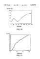
- FIG. 9is a graph depicting the plasma current density at the substrate location according to the example of FIG. 5A using the plasma source depicted in FIG. 3 as a function of magnetic field in the source region.
- FIG. 10is a graph of the same data as in FIG. 9 but graphed on a linear scale for magnetic field to show the plasma current density at the substrate location where the magnetic field is low, varying from zero to 160 gauss.
- FIG. 11is a graph depicting the total plasma current (or total flux) at the substrate location according to the invention as depicted in FIG. 5A using the plasma source as depicted in FIG. 3 as a function of RF power to the source at a gas pressure of 2 mtorr.
- FIG. 12is a graph depicting the plasma current density at the substrate location according to the invention as depicted in FIG. 5A using the antenna as depicted in FIG. 3 as a function of the gas pressure.
- FIG. 13is a graph depicting the plasma current density at the substrate location according to the invention as depicted in FIG. 5A and the plasma source of FIG. 3 as a function of position to show the excellent uniformity over a substantial width.
- FIGS. 14A to 14Care diagrams showing the arrangement of the electromagnetic system in the plasma generator region according to the present invention to make efficient the transport of plasma from the plasma generator tube to the substrate process chamber which includes a magnetic bucket and where uniformity and high plasma flux to the substrate are required.
- FIG. 15Ais a plot of the magnetic field lines obtained using one electromagnet surrounding the plasma source tube.
- FIG. 15Bis a plot of the magnetic field lines obtained using two electromagnets surrounding the source tube and where the outer magnet coil carries a current in the opposite direction from the inner magnet coil and has a coil current that is 40% as large in magnitude as that of the inner coil.
- FIG. 16Ais a schematic diagram of the configuration of a plasma etching or deposition apparatus.
- FIG. 16Bis a plan view of the substrate process chamber section of the arrangement of FIG. 16A taken along the line 7A--7A in FIG. 16A.
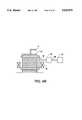
- FIG. 17Ais a plan view of the substrate process chamber showing the gas feed lines, the nozzle holes for gas injection into the chamber, the water cooling lines and the grooves for the ceramic permanent magnets.
- FIG. 17Bis a detail showing the entrance to the gas feed line at the top of the substrate process chamber shown in FIG. 17A.
- FIG. 17Cshows in larger size the gas feed structure of FIG. 17A.
- FIG. 18is a cross sectional SEM image obtained for the etching of poly-Si in pure Cl 2 using the MORI plasma source etching system.
- the SEMshows structure with 100% overetch.
- FIG. 19shows the aluminum etch rate, the oxide etch rate, and the PR etch rate (left ordinate) and selectivity to photoresist etching and to oxide etching (right ordinate) as a function of RF wafer bias power applied at 13.56 MHz.
- the gas mixtureis 85% Cl 2 -15% BCl 3
- the MORI source poweris 1 KW
- the substrateis located in the process chamber 20 cm below the end of the source tube.
- FIG. 20is a cross sectional SEM image obtained for sub micron etching of W on a TiW adhesion layer on thermal oxide in pure SF 6 using the MORI plasma source etching system.
- the anisotropyis excellent, there is no CD loss, and there are no residues.
- FIGS. 1A, 2B, and 2Cillustrate schematically the RF current flow in two antennas constructed according to the invention disclosed in U.S. Pat. No. 4,990,229 issued Feb. 5, 1991.
- U.S. Pat. No. 4,990,229is incorporated herein by reference in its entirety.
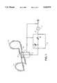
- FIG. 3A simplified view of principal elements and relationships in a device in accordance with the invention is provided by the representation of FIG. 3, wherein high density plasma 9 is to be generated within a source tube 10 of generally cylindrical form about a central (here vertical) axis.
- an injector 11feeds gas to be ionized into the interior volume of the source tube, where the gas is excited by an external loop antenna 12 that encompasses an intermediate region of the source tube 10.
- the antenna loop 12comprises in this example a not fully circular element lying in a plane that is at 90° or less in either sense relative to the central axis.
- the direction of propagation of the plasmais here downward toward an exit aperture 13.
- the antenna loop 12has its opposite ends coupled to the outer conductor 14 and center conductor 15 of a coaxial driver line 16 which is energized through a matching box 18 by an RF energy source 19.
- a pair of variable vacuum capacitors 20, 21 in the matching box 18are adjustable to tune the circuit so that the antenna loading plus the reactive load of the matching box 18 is approximately 50 ohms to minimize the reflected power.
- the antenna tuning and wave spectrumare adjusted to match the conditions in the plasma field, and also in relation to an interior axial magnetic field 8 generated by at least one magnetic field coil (not shown) about the source tube 10.
- the matching conditionis predicted by theory to be dictated by the dispersion relation:
- the antenna loop 12is driven at 13.56 MHz and with RF energy of the order of 2.0 KW (in the range of 100 W to 5 KW) by the RF energy source 19.
- the magnetic field established by the magnetic field coilis in the range of 10 to 1000 gauss, for different useful applications.
- the gasis argon and maintained at a pressure of about 1 mtorr in this example.
- reactive gasessuch as SF 6 , chlorine, oxygen, and mixtures with oxygen have been used with comparably useful results.
- a pressure range of 0.1 mtorr to 200 mtorrcan be used if other variables are properly taken into account.
- the looped portionsmust describe a helical path in order to establish a helical wave property, but this is disproven by the results given below as to the efficacy of the present invention. It is important, however, that the antenna loop 12 be sufficiently spaced apart from the closed (gas entry) end of the source tube 10 for the necessary interactions to occur between the plasma and the RF energy, and for the dispersion relation to be satisfied so that proper excitation can be realized and high density can be achieved. Too long a length, however, can also preclude establishment of the proper wave numbers. In practice source tubes 10 of 1" to 4" in diameter and 8" to 9" in length have been used, with the antenna loop being about one-third or more of the distance from the closed end.
- Eis the electric field
- Bis the magnetic field
- iis the current density
- B ois the vacuum magnetic field
- eis the charge on an electron
- n ois the density of the plasma
- ⁇is the resistivity of the plasma.
- J mis a Bessel function of the first kind
- J m 'is a derivative of J m with respect to its argument
- ais the plasma radius
- Tis a transverse wave number defined by
- mis the mode number that describes the ⁇ dependence of perturbations of the form B exp(i(m ⁇ +k z - ⁇ )).
- ⁇ ccyclotron angular frequency
- Landau dampingis a collisionless damping of waves in a plasma due to particles in the plasma that have a velocity nearly equal to the phase velocity of the wave. These particles travel with the wave, do not see a rapidly fluctuating electric field and so can effectively exchange energy with the wave.
- a plasmathere are electrons both faster and slower than the wave.
- a Maxwellian distributionthere are more slow electrons than fast ones and so there are more particles taking energy from the wave than vice versa.
- the damping rate due to Landau dampinghas been calculated by Chen for helicon waves and can be expressed as:
- the frequency of the wavesshould be such that it satisfies ⁇ c ⁇ c where ⁇ c is the ion cyclotron frequency, eB o /M i and ⁇ c is the electron cyclotron frequency eB o /M. These waves are low frequency waves that operate far below the electron cyclotron frequency.
- the mode structure of the wave electric and magnetic fieldsshould be understood so that the antenna arrangement can efficiently couple the RF power into wave excitation.
- the wavecan be efficiently excited in this mode with an antenna that has a single loop located in a plane perpendicular to the magnetic field generating a spectrum of wave numbers such that a portion of the spectrum generated includes 2 ⁇ /k z , where k z is given by the stated dispersion relation.
- the electric field vectorrotates in a righthanded sense, i.e., it rotates clockwise as it travels along B o which is in the z direction.
- This modecan be excited with the present invention if the single loop is canted at an angle to the magnetic field such that the wave spectrum generated contains a significant portion around 2 ⁇ /k z , where k z is given from the dispersion relations.
- the efficiency of plasma productiondepends on the coupling of RF energy into the plasma. As discussed above, the important mechanism for damping of the RF energy is believed to be Landau damping.
- the higher the value of k zthe higher the density.
- the phase velocity of the waveis ⁇ /k z and so increasing k z decreases the energy of the electrons that are accelerated by the wave. If the k z is too high, then the energy of the electrons may fall below the ionization potential. It is therefore important to control k z in order to be able to increase the density and control the electron temperature.
- the present inventionuses low frequency whistler waves to generate plasmas with high density exceeding 10 13 per cm 3 .
- the frequency of excitationwas 8 MHz, and the density profile of the 10 cm plasma was found to be quite peaked, particularly at the higher magnetic field strengths needed for high densities.
- Chen, in an Australian National University reportexplained the mechanism as Landau damping.
- the Z axis wave number, k zvaries as the ratio n/B, and inversely with wavelength ⁇ , requiring a longer source tube. Conversely, if B is decreased, the plasma density is relatively higher because the shorter wavelengths function to create needed wave numbers regardless of tube size.
- FIG. 4AThe basic configuration of a plasma deposition or etching apparatus according to the present invention is shown in FIG. 4A.
- the plasma generation chamber 10'is cylindrical in shape and is made of a non-conducting material such as quartz or pyrex.
- the antenna 12'is mounted at an inclination to the longitudinal axis of the chamber 10' as described in conjunction with FIG. 3.
- An axial magnetic fieldis provided by magnetic field coils 24 and 25 as shown in FIG. 4A, but the plasma can also operate using only one of these coils.
- the plasmais transported by the magnetic field to a separate process chamber 27.
- the shape of the plasma emerging into the process chamber 27can be controlled by varying the amount and direction of the current made to flow in a coil 28 about the exit of the chamber 27.
- a substrate 30 to be coated or etchedis mounted on a substrate holder 31 which is electrically isolated. Plasma that bombards the substrate 30 causes the substrate 30 to reach a negative self bias of between 0 and 10 V. For some films to be formed, it is advantageous for the film to be bombarded by ions with greater energy than they would obtain due to the self-bias. In this case, it is desirable to apply RF power from a second RF source 33 through a second matching circuit 34.
- the substrate holder 31is a copper block that is cooled or heated by a heating/cooling circuit 35. Gas is injected via a stainless steel injection tube 11' connected to the source for the plasma generation chamber 10'. A stainless steel ring 36 has a diameter that is large compared to the size of holes 37 that are distributed equally around the ring 36. This arrangement is such that a uniform flow of gas is directed towards the substrate 30.
- the RF voltageis applied to the antenna 12 by means of a matching circuit 18 and RF source 19, as described in conjunction with FIG. 3. Tuning in the matching circuit 18 is used to maximize the power that is coupled into the plasma and minimize the power that is reflected back along a 50 ohm cable 38 to the RF power supply 19.
- FIG. 4Bshows a plasma generation chamber 10' with a gas inlet 11.
- An RF power supply 19'provides, through an RF matching circuit 18', RF power to antenna 32.
- This matching circuit 18'maximizes the power coupled into the plasma and minimizes the power that is reflected back along cable 38 to the RF power supply 19'.
- Magnetic field coil 26is the single magnet used to create the axial magnetic field to transport the plasma to a separate process chamber (not shown) located beneath the plasma generation chamber 10'.
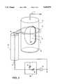
- FIG. 5Ashows an arrangement where high uniformity over a large area is required.
- the plasma generation chamber 10'is cylindrical in shape and is made of a non-conducting material such as quartz, pyrex, alumina or sapphire.
- the plasma generation chamber 10'(which is also called the belljar) is constructed of quartz when the working gas is chlorine, oxygen, all halogens except those containing fluorine, and halogenated hydrocarbon compounds except for those containing fluorine. Gases not containing fluorine are found not to etch quartz and therefore quartz is a preferred material. When gases containing fluorine are used with a quartz belljar, the fluorine atoms etch the quartz and may produce particulates that can contaminate the wafer surface. The etching of the quartz also undesirably releases oxygen into the plasma that interferes with the processing of the wafers.
- quartzis the preferred belljar material when etching polysilicon and metals such as aluminum or copper using etching gases such as Cl 2 , a mixture of Cl 2 and O 2 , HBr, a mixture of Cl 2 and HBr, BCl 3 , a mixture of Cl 2 and BCl 3 , N 2 , a mixture of N 2 and SCl.sub. 4, and so on.
- the plasma generation chamber (belljar) 10'is constructed of either alumina or sapphire, which materials are found to resist erosion by chemical etching in the presence of fluorine-containing gases.
- the antenna 12is mounted at an angle less than the perpendicular, but otherwise corresponds to the configuration described in FIG. 3.
- An axial magnetic fieldis provided by the magnetic field coils 24 and 25.
- the plasmais transported by the magnetic field to a process volume comprising a part of a magnetic bucket chamber 40.
- the wall 41 for the magnetic bucket 40is made of stainless steel or aluminum and can be of, for example, circular or rectangular cross-section. In a preferred embodiment, the wall 41 is made of anodized aluminum. In either case the interior dimensions of the magnetic bucket 40 are such that it is larger than the interior diameter of the plasma generation chamber 10'.
- the magnetic field within the magnetic bucket 40is provided by a number of permanent magnets 43 arranged with their poles perpendicular to the wall 41 of the magnetic bucket 40 and with alternating north N and south S poles.
- the number of permanent magnets 43 to be used with the magnetic bucket 40involves a trade off between achieving a uniform plasma density in the vicinity of the substrate or wafer, and the cost and complexity of providing additional permanent magnets 43.
- Each additional set of north N and south S pole magnetsprovides additional uniformity in the density of the plasma.
- each additional set of magnetsalso adds to the cost and complexity of the magnet bucket 40.
- the number of permanent magnets usedis within the range 16 to 28. In the preferred embodiment of the invention, 24 magnets are used. Twenty-four magnets was found to yield the optimum balance between plasma density uniformity, cost and complexity.
- the use of 24 magnetsallows uniform etching, sputtering or deposition of layers on 150 mm (6 inch) and 200 mm (8 inch) wafers.
- the optimum number of magnetsis still between 16-28; however, a smaller process chamber would be used.
- the optimum distance between the end of the plasma generation chamber 10' and the substrate 45is between 150-200 mm.
- a substrate 45 to be coated or etchedis mounted on a substrate holder 46 at the lower region of the plasma field in the magnetic bucket 40.
- the substrate holder 46is a copper block that is cooled or heated by a heating/cooling circuit 47.
- gasis injected via stainless steel or anodized aluminum tube 11' connected to the gas source for the plasma generation chamber 10', and into the magnetic bucket 40 via a stainless steel or anodized aluminum ring 36 that is connected to the gas feed and includes small diameter holes 37 that are distributed equally around the ring 36.
- a uniform flow of plasmais directed towards the substrate 45, as an RF voltage from a power supply 19 is applied to the antenna 12 by means of a matching circuit 18 which consists of two vacuum capacitors as described in FIG. 3.
- FIG. 6Ashows an arrangement where high uniformity over large rectangular shaped areas is required such as needed in the coating of large flat displays.
- the plasma generator unitsare of the type described above, but, in this arrangement, multiple generators may be used depending on the size and shape of the plasma needed.
- FIG. 6Athree plasma generation chambers 49, 50 and 51 are shown, disposed along the central axis of the top of a process chamber.
- Each plasma generation chamber 49, 50 or 51is cylindrical in shape and made of non-conducting material such as quartz, pyrex, alumina or sapphire and each includes a separate single loop antenna 52, 53 or 54 of the type described in FIG. 3.
- the antennas 52, 53, 54are coupled in electrical series to the matching box 18 and RF power supply 19, so that equal RF current flows are assured.
- An axial magnetic field for each plasma generation chamber 49, 50 or 51is provided by magnetic field coils 55 and 56, 57 and 58, or 59 and 60, respectively.
- the plasmas thus separately generatedare transported by the magnetic field into a common rectangular magnetic bucket chamber 61.
- the plasmasdiffuse along the field lines and expand to fill the magnetic bucket chamber 61.
- the magnetic field within the magnetic bucket chamber 61is provided by permanent magnets 62 arranged with their poles perpendicular to the surface of the magnetic bucket chamber 61 and with alternating N and S poles.
- the magnetic field pattern provided by the magnetsis shown in FIG. 6B.
- the substrate 63 to be coated or etchedis mounted on a substrate holder 64 which is electrically isolated. Plasma that bombards the substrate causes the substrate to reach a negative self bias of between 0 and 10 V. For some films to be formed or in some etching applications, it is advantageous for the substrate 63 to be bombarded with energetic ions. In this case it is desirable to apply RF power from a second RF power supply (not shown) through a matching circuit to the substrate holder 64, which again may be a copper block that is cooled or heated by a heating/cooling circuit 65.
- a second RF power supplynot shown
- FIG. 7Ais another example of a device in accordance with the invention, for providing additional control of plasma uniformity over a large area.
- the plasma generating chamber 10'is cylindrical in shape, of non-conducting material such as quartz or pyrex, and surrounded by an antenna 12' at an angle less than 90°.
- An axial magnetic fieldis provided in the source region by the magnetic field coils 69 and 70 or by only one such coil.
- the plasmais transported by the magnetic field from the source to a magnetic bucket chamber 71 which is substantially of the same design as described for FIG. 5A.
- an additional magnetic field coil 72concentric with the central axis of the plasma generating chamber 10' is located below the substrate holder 74 which is cooled or heated by a heating/cooling circuit 75.
- the permanent magnets 76 about the magnetic bucket chamber 71are arranged as described earlier in FIG. 4 and create a magnetic cusp field 77 as seen in FIG. 7B.
- the additional magnetic field coil 72is made to carry a current in the direction opposite to that of the currents made to flow in coils 69 and 70. The effect is to create another magnetic cusp, now a ring cusp, located approximately in the plane of the substrate 78, such plane being substantially perpendicular to the line cusps created by the North-South permanent magnets 76.
- Gasis injected as above by an injection port 11 into the plasma generation chamber 10' and by another feed tube 11' through a stainless steel ring 36 into the bucket chamber 71.
- the ring 36has a diameter large compared to the size of holes 37 directing a uniform flow of gas to the substrate 78.
- the ring 36can also be the gas feed for the source when the main feed is not used.
- Small amplitude variations with time in the current flowing in the coil 72are generated by a modulating driver 73 to cause the ring cusp plane to fluctuate up and down about the plane of the substrate 78, thereby time averaging the plasma profile incident across the substrate and further enhancing uniformity.
- This approach of using the time-variation of a bottom coilcan also be employed to enhance uniformity when a magnetic bucket is not employed by using the arrangement shown in FIG. 4A and by running the current in coil 28 in the exit region therein opposite to that in coils 24 and 25 at the plasma generation chamber 10', thereby creating the ring cusp in the plane of the substrate as just described.
- FIG. 8is another exemplification according to the present invention that is suitable for using the RF generator system in conjunction with a sputter target.
- the plasma generator chamber 10"is cylindrical in shape, of nonconducting material, and surrounded by an antenna 12' mounted in a plane perpendicular to the longitudinal axis, as in the example of FIG. 3.
- An axial magnetic fieldis provided by the magnetic field coils 80 and 81 about the plasma generator chamber 10" and the magnetic field coils 82 and 83 about a process chamber 91.
- the plasma 90is transported from the plasma generator chamber 10" into the process chamber 91 and flows along the magnetic field to a lowermost sputter target 93 which is biased to a large negative voltage (about -700 V) by a power supply 94.
- a DC power supplyis used to maintain a charge when the substrate holder is conductive, but if the substrate holder is non-conductive an alternating current power supply is employed instead.
- the plasma diameteris made to conform to that of the sputter target 93 by controlling the magnetic field.
- the material sputtered from the sputter target 93is deposited on the substrates 96 juxtaposed about it.
- a horizontal baffle 97 in a plane above the sputter target 93may be used to control the gas pressure near the substrates 96 and other gases may be introduced near the substrates 96 through outlet 98.
- the substrates 96are mounted on a substrate holder 101 and are positioned above the sputter target 93.
- the substrate holder 101can rotate about the vertical axis to enhance uniformity of deposition of sputtered material.
- the substrate holder 101has a central aperture to permit plasma to pass along the magnetic field from the plasma generator chamber 10" to the sputter target 93.
- FIG. 9Data is shown in FIG. 9 on the plasma current density measured in mA/cm 2 produced according to the present invention in the arrangement shown in FIG. 5A using the antenna shown in FIG. 3 and measured by using a fast-injection Langmuir probe at a location just above the plane of the substrate.
- the vertical axisrepresents plasma current density and the horizontal axis represents magnetic field strength in FIG. 9 and in FIG. 10 below.
- the RF frequencywas 13.56 MHz and was supplied using a commercial RF power supply generating 2.0 KW passing through a matching box as shown in FIG. 3.
- Datawas obtained for the plasma current density as a function of magnetic field in the plasma generation chamber 10' from zero to 1000 gauss.
- the data for field varying from zero to 160 gaussis shown in FIG. 10.
- the gas pressureis about 1 mtorr.
- a substantial current density approaching 40 mA/cm 2is found at a low value of field equal to 20 gauss.
- Increase of the magnetic field to 100 gauss and abovealso produces high values of plasma current density, achieving levels of 140 mA/cm 2 .
- FIG. 11data is shown for the total plasma flux (vertical axis) measured in Amperes reaching the substrate plane as a function of RF power (horizontal axis) measured in KW for a gas pressure of 2 mtorr and a magnetic field in the source chamber of 250 gauss.
- the total flux achievedis over a diameter of 8 inches (20 cm).
- the total flux incident onto the substratereaches as high as 15 Amperes from a source with a chamber diameter of about 4" (10 cm).
- FIG. 12depicts operation of the plasma source (plasma current density measured in mA/cm 2 along the vertical axis) in the arrangement described in FIG. 5A with the antenna as described in FIG. 3 as a function of gas pressure (horizontal axis) in the chamber, demonstrating that the source operates effectively at low pressures (below 1 mtorr) up to higher pressures.
- the sourcehas been run successfully at pressures greater than 100 mtorr.
- the uniformity of the plasmais shown in FIG. 13, said uniformity measured at a distance 6" below the exit of the plasma generation chamber 10' in the magnetic bucket 40 with a substrate 45 in place using the arrangement shown in FIG. 5A and the antenna 12 as depicted in FIG. 3.
- the vertical axisshows plasma current density measured in mA/cm 2 and the horizontal axis shows the position within the substrate process chamber measured in centimeters.
- the magnetic field in the plasma generation chamber 10'is 150 gauss, and the pressure is about 2 mtorr.
- the plasmais highly uniform over a width exceeding 8" (20 cm).
- a similar degree of uniformityis achieved using the cusp magnetic arrangement depicted in FIG. 7A, employing the magnetic field coil 72 carrying a current in a direction opposite to the current flowing in the magnetic field coils 69 and 70.
- systems and devices in accordance with the inventionprovide uniform plasmas utilizing low frequency whistler wave excitations using a single loop antenna with a plasma generation chamber.
- an extended plasma in a plasma generation chambercan cover a wide area of shaped areal characteristic, if desired, with high plasma current density and high total plasma flux. Both low and high magnetic field strength modes are sustainable, and etching, deposition and sputtering processes can be employed.
- FIG. 16Ais a schematic diagram of a configuration of a plasma etching or deposition apparatus.
- FIG. 16Bis a plan view of a substrate process chamber section of the arrangement of FIG. 16A taken along the line 7A--7A in FIG. 16A.
- gas feed 141enters plasma generator tube 131 near the top of plasma generator tube 131.
- Inner magnet coil 133 and outer magnet coil 134surround plasma generator tube 131.
- RF antenna 132surrounds plasma generator tube 131.
- RF power supply 148provides, through an RF matching box 146, RF power to RF antenna 132.
- Plasma generator tube 131is attached to the top of substrate process chamber 135.
- a capacitor 201is formed adjacent plasma generator tube 131.
- a clamp 202 and a collar 203help hold magnet coils 133 and 134 in place on base plate 204.
- Gasis fed through gas feed line 205 into substrate process chamber 135 through gas injection nozzle 206.
- a plurality of ceramic magnets 207surround substrate process chamber 135, as best shown in FIG. 16B.
- a pump 208adjoins substrate process chamber 135 near the bottom 135a of substrate process chamber 135.
- a chuck motor 212, lead screw 211 and chuck actuator 210move a chuck 218 up and down within substrate process chamber 135.
- a wafer substrate 219is held in place on chuck 218 by clamp ring 224. Cooling water enters substrate process chamber 135 and travels to chuck 218 along path 216 and exits along path 215.
- Helium for cooling wafer substrate 219enters substrate process chamber 135 along path 214.
- RF power supply 213supplies power to chuck 218.
- a metal bellows 209encloses an area underneath chuck 218.
- a gate valve 217is formed on the side of substrate process chamber 135 opposite the side on which pump 208 is formed.
- a DC power supply 221controls separation unit 222 to control the flow of cooling water along path 220. As seen in FIG. 16B, cooling water holes 223 are formed in bottom 135a of substrate process chamber 135.
- the inventionrelies on the use of a double set of magnet coils 133 and 134 with an inner magnet coil 133 of smaller diameter and an outer magnet coil 134 of larger diameter located around the inner magnet coil 133 in order to produce the magnetic field for use with an RF plasma generator described in U.S. Pat. Nos. 4,990,229 and 5,122,251 in order to transfer plasma more efficiently from the plasma generator tube 131 to the substrate 219 that is located in the substrate processing chamber 135 of FIG. 16A.
- the principle types of antenna 132 used to generate plasma in the plasma generator tube 131are shown in FIGS. 1, 2, and 3.
- the substrate processing chamber 135is surrounded by a multipolar set of permanent magnets 207, shown in FIG.
- the distance between the end of the plasma generator tube 131 and the substrate 219is typically 160 mm at the maximum or less, without sacrificing plasma uniformity or intensity.
- the plasma uniformityis generally less than 2% (1 sigma) at the substrate location.
- the distance between the end of the plasma generator tube 131 and the substrate 138is generally between 10 cm and 20 cm and can be adjusted to achieve a required uniformity by adjusting the current in the outer magnet coil 134 relative to the amount of current to the inner magnet coil 133 shown in FIG. 16A and FIGS. 14A and 14B.
- An earlier and common designinvolves using only one magnet 26 in the schematic arrangement shown in FIG. 4B.
- FIG. 15Ashows the magnetic field pattern which results from 1OOA of current flowing only in the inner magnet coil 133 of FIGS. 14A and 14B.
- the lines 139 of magnetic fieldare shown to extend well below the plasma source tube and into the process chamber region below.
- Magnetic field line 139ais the first magnetic field line 139 to intersect the wall of plasma generator tube 131.
- These magnetic field lines 139curve more rapidly in FIG. 15B towards the side walls once leaving the source tube region.
- Another objective of this inventionis to provide a means of shielding inner magnet coil 133, or inner magnet coil 133 and outer magnet coil 134 from pickup of RF power from the antenna 12 or 12' or 32 or 132.
- Such RF pickupcan cause a false signal to the control system of the DC power supply which drives the current in the magnet coils 133 and 134 and lead to unreliable electromagnet operation.
- the RF power pickup in the magnet coils 133 and 134is reduced by a factor of more than 1000 by wrapping each magnet coil 133 and 134 with a thin sheet of conducting material.
- a simple and preferred means of providing such shieldingis to use aluminum tape to wrap the magnet coils 133 and 134, whether there is one or more than one magnet coil 133 or 134.
- FIG. 4AA system with one magnetic field coil 25 in the plasma generation region is shown in FIG. 4A and another system with one magnetic field coil 26 in the plasma generation region is shown in FIG. 4B.
- a plasma generation system with double magnet coils 133 and 134is shown in FIGS. 14A and 14B.
- Another objective of this inventionis to provide a means to inject gas into the substrate process chamber 135 (best shown in FIG. 14B) so as to eliminate the need for a separate gas feed system such as a gas feed ring and to minimize particle formation in the substrate process chamber 135 by eliminating extra surfaces in the substrate process chamber 135 and by permitting the inside of the substrate process chamber 135 to be smooth and without corners.
- the main housing of the substrate process chamber 135is a single piece of stainless steel, aluminum, or anodized aluminum in the shape of a cylinder that has sides, an open bottom and a top containing a hole about the cylinder axis which serves as the exit hole and interface with the plasma generator tube 131.
- anodized aluminumis used for the main housing.
- the plasma generator tube 131is preferably made of quartz or alumina and attaches to the top of the substrate process chamber 135.
- the substrate process chamber wallsare preferably about 250 mm in thickness. Holes in the form of tubes are created in the top cover of the cylinder approximately 150 mm below the top of the cylinder and in a plane perpendicular to the axis of the cylinder. The interior of the tubes is anodized.
- a preferred form of these gas feed linesis a diamond pattern shown in FIG. 17A in which each tube cutout 171 is approximately tangent to a circumference of a circle whose radius is equal to the substrate radius. Gas outlet nozzles are inserted into tap holes drilled into the top plate so as to connect to the gas feed lines in the top section of the substrate process chamber.
- the nozzle piecesare removable for cleaning and have smooth external surfaces to minimize particulate formation.
- the nozzlesare made of either stainless steel or anodized aluminum.
- Gasis fed from one or more feed sites into the tube lines in the top of the single piece cylindrical substrate process chamber to permit control of the pressure in the tube lines and the gas release rate from each nozzle regardless of wafer size.
- gasis preferably fed at one entrance hole in the top of the cylindrical substrate process chamber and four nozzles are used to release the gas uniformly towards the substrate. Excellent rates and uniformity are achieved and separate gas feed 141 into the plasma generator tube 131 is not required for most etch process applications.
- a primary reactive gasis fed through the tubes or through a separate gas ring into the substrate process chamber and a second and usually less complex gas such as argon, helium, nitrogen, or oxygen is fed through the gas feed 141 directly into the plasma generator tube 131.
- a second and usually less complex gassuch as argon, helium, nitrogen, or oxygen is fed through the gas feed 141 directly into the plasma generator tube 131.
- FIG. 18is a scanning electron microscope image of a doped and patterned polysilicon wafer consisting of photoresist on a 4000 ⁇ polysilicon layer over a 1000 ⁇ thermal oxide film.
- the feature sizeis 0.4 microns.
- the etching process in chlorineis at 2.3 mtorr and consists of three steps: a 20 second punchthrough; a 40 second main etch with a source power of 3 KW and a wafer bias power of 38 W; and a 100% overetch step at a source power of 1 KW and a wafer bias power of 20 W.
- the poly-Si etch rateis 3170 ⁇ /m, the selectivity to oxide is about 90 and the selectivity to photoresist exceeds 10.
- the etching of the metal film Al--Si--0.5 Cu by pure Cl 2 and Cl 2 --BCl 3 mixtures in this plasma source etching systemhas also been carried out using patterned wafers with 1 micron feature size and consisting of photoresist on a 10,000 ⁇ Al film over a 1000 ⁇ thermal oxide layer. Uniform etching at rates ranging from 5000 ⁇ /m to 12,000 ⁇ /m are achieved. Results at 3 mtorr in an 85% Cl 2 --15% BCl 3 mixture using 1 KW of source power are shown in FIG. 19 as a function of RF bias power applied to the wafer.
- the Al film etch rateis essentially independent of bias power, but the selectivity to oxide and to photoresist increase sharply with decreasing bias power.
- the Al etch rateis about 6500 ⁇ /m while the selectivity values are very high: 22 to 1 for selectivity to oxide etching and 9 to 1 for selectivity to photoresist etching.
- the etch rateincreases with source power, BCl 3 addition, and gas pressure. The selectivity increases with decreasing bias power while good, anisotropic etching is achievable in both pure Cl 2 and Cl 2 --BCl 3 gases.
- Preferred operating condition and source-coil currentscan depend on working gas, source power, wafer bias power, and gas pressure. For example, in the etching of tungsten using fluorine-containing gases such as SF 6 , it is found that the optimum outer magnet coil 134 to inner magnet coil 133 current ratio is closer to 1 for etching at a pressure of about 3 mtorr.
- patterned tungsten waferswere etched in the plasma source etching system using pure SF 6 .
- the wafers usedhad a dry-developed photoresist over a 5500 ⁇ W layer over a 500 ⁇ TiW layer on a 1000 ⁇ thermal oxide layer.
- the feature sizevaries from 0.27 micron to about 1 micron.
- Both a one-step and two-step processhave been investigated. In the one-step process at 3 mtorr, the source power is 1 KW and the wafer bias power is 50 W. In the two-step process at 3 mtorr, the source power is 1.5 KW but the wafer bias power is first 25 W and then 65 W.
- a uniform, anisotropic etch of W over TiWis achieved along with very good etch rates and high values of selectivity to both photoresist and oxide.
- the etch rateis 2770 ⁇
- the preferred processis a two-step process with the bias power in the second step reduced to 50 W to yield an etch rate of 2770 ⁇ /m with a selectivity value greater than 2 for W to PR and greater than 10 for W to oxide.
- the etchingis highly anisotropic with minimal CD loss and no residues as illustrated by the SEM shown in FIG. 20.
- Table 1illustrates a number of different uses of the plasma deposition or etching apparatus of this invention when used to etch a substrate.
- Table 1lists various combinations of gases to be fed into the source region of the plasma generation apparatus corresponding to plasma source 131 in FIG. 16A and into the process chamber region corresponding to substrate process chamber 135 in FIG. 16A. Pure chlorine provides a preferred gas for use in etching at 1.5 to 2 mtorr in the structure of FIG. 16A.
- a number of different gasesare suitable for use in the apparatus of this invention when used to etch selected materials of a type commonly used in the fabrication of semiconductor devices.
- the apparatus of this inventionis suitable for use for any of a variety of purposes, including the etching of metals and other materials suitable for use in numerous applications.
- the preferred gases for use in the apparatus of this inventionare freon and methane.
- an optimum gasis chlorine (Cl 2 ) at 90-95% volume and boron trichloride (BCl 3 ) at 5-10% and at a pressure of 2 to 3 mtorr.
- Table 2gives a number of different gases or combinations of gases to be fed into plasma generator tube 31 in FIG. 16A and a number of different gases or combinations of gases to be fed into substrate process chamber 135 shown in FIG. 16A.
- the particular film to be depositedis illustrated in the leftmost column and the gases to be used in both plasma generator tube 131 and substrate process chamber 135 are listed in the second and third columns.
- plasma generation chambersin which plasma is generated and a wafer or substrate is not disposed may be formed from quartz, pyrex, sapphire or alumina.
- the process chamberi.e., chamber in which the wafer or substrate is disposed
- the magnetic bucketis formed of anodized aluminum.
Landscapes
- Chemical & Material Sciences (AREA)
- Engineering & Computer Science (AREA)
- Physics & Mathematics (AREA)
- Plasma & Fusion (AREA)
- Analytical Chemistry (AREA)
- Chemical Kinetics & Catalysis (AREA)
- General Chemical & Material Sciences (AREA)
- Materials Engineering (AREA)
- Mechanical Engineering (AREA)
- Metallurgy (AREA)
- Organic Chemistry (AREA)
- Drying Of Semiconductors (AREA)
- Plasma Technology (AREA)
Abstract
Description
[ω/ω.sub.c -ω.sub.p.sup.2 /C.sup.2 K.sub.z.sup.2 ].sup.2 =1+(3.83/k.sub.z a).sup.2
∇×E=δB/δt, ∇×B=μ.sub.o i, ∇. B=0E=i×B.sub.o /en.sub.o, E.sub.z =ηJ.sub.z
∇.sup.2 B+α.sup.2 B=0 where α=(ω/k) (μ.sub.o en.sub.o /B)
mαJ.sub.m (T a)+TkaJ.sub.m ' (T a)=0
T.sup.2 =α.sup.2 -k.sup.2
J.sub.1 (T a)=0 (m=0)
J.sub.1 (T a)=T k a/2 α(J.sub.2 -J.sub.0) (m=1)
[(ω/ω.sub.c)-(ω.sub.p.sup.2 /C.sup.2 k.sub.z.sup.2)].sup.2 =1+(3.83/k.sub.z a).sup.2
Damping Rate=Jm(k.sub.z)/Re(k.sub.z) 2πc.sup.2 (3.8/a).sup.2 ξ.sup.3 e-ξ.sup.2
n=αB.sub.o k.sub.z (T.sub.2 +k.sub.z.sup.2).sup.1/2
TABLE 1 __________________________________________________________________________Etching (Operating Pressure Range; 0.5 to 10 mtorr) (Optimum Pressure Range; 1-3 mtorr) Gas or Gas or Combination of Combination of Gases Fed into Gases Fed into Process Chamber Etching Substrate Source Region 1 Region 2 or 3 __________________________________________________________________________ Etching of Polysilicon A. Doped Polysilicon Cl.sub.2 ; SF.sub.6, CF.sub.4 ; and/or Cl.sub.2 ; SF.sub.6 ; CF.sub.4 ; Gate Etch Cl.sub.2 + O.sub.2 ; SF.sub.6 + O.sub.2 ; Cl.sub.2 + O.sub.2 ; SF.sub.6 + O.sub.2 ; or CF.sub.4 + O.sub.2 ; CF.sub.4 + O.sub.2 ; He plus He B. Undoped Polysilicon Cl.sub.2 ; SF.sub.6, CF.sub.4 ; and/or Cl.sub.2 ; SF.sub.6 ; CF.sub.4 ; Gate Etch Cl.sub.2 + O.sub.2 ; SF.sub.6 + O.sub.2 ; Cl.sub.2 + O.sub.2 ; SF.sub.6 + O.sub.2 ; or CF.sub.4 + O.sub.2 ; CF.sub.4 + O.sub.2 ; He plus He C. Polysilicon Buffer Cl.sub.2 ; SF.sub.6, CF.sub.4 ; and/or Cl.sub.2 ; SF.sub.6 ; CF.sub.4 ; Layer Etching (PBL) Cl.sub.2 + O.sub.2 ; SF.sub.6 + O.sub.2 ; Cl.sub.2 + O.sub.2 ; SF.sub.6 + O.sub.2 ; or CF.sub.4 + O.sub.2 ; CF.sub.4 + O.sub.2 ; He plus He D. Spacer Etching (Etch Cl.sub.2 ; SF.sub.6, CF.sub.4 ; and/or Cl.sub.2 ; SF.sub.6 ; CF.sub.4 ; of Lightly Doped Cl.sub.2 + O.sub.2 ; SF.sub.6 + O.sub.2 ; Cl.sub.2 + O.sub.2 ; SF.sub.6 + O.sub.2 ; Drains or LDD) or CF.sub.4 + O.sub.2 ; CF.sub.4 + O.sub.2 ; He plus He E. Polysilicon Trench Cl.sub.2 ; SF.sub.6, CF.sub.4 ; and/or Cl.sub.2 ; SF.sub.6 ; CF.sub.4 ; Etching Cl.sub.2 + O.sub.2 ; SF.sub.6 + O.sub.2 ; Cl.sub.2 + O.sub.2 ; SF.sub.6 + O.sub.2 ; or CF.sub.4 + O.sub.2 ; CF.sub.4 + O.sub.2 ; He plus He F. Planarization of Cl.sub.2 ; SF.sub.6, CF.sub.4 ; and/or Cl.sub.2 ; SF.sub.6 ; CF.sub.4 ; Polysilicon (Blanket Cl.sub.2 + O.sub.2 ; SF.sub.6 + O.sub.2 ; Cl.sub.2 + O.sub.2 ; SF.sub.6 + O.sub.2 ; Etching) or CF.sub.4 + O.sub.2 ; CF.sub.4 + O.sub.2 ; He plus He Etching Silicon Nitride (Si.sub.3 N.sub.4) A. Etching of Plasma- SF.sub.6 ; CF.sub.4 ; O.sub.2 ; CHF.sub.3 and/or SF.sub.6, CF.sub.4, O.sub.2, deposited Si.sub.3 N.sub.4 Pads SF.sub.6 + O.sub.2 ; CF.sub.4 + O.sub.2 ; CHF.sub.3, SF.sub.6 + O.sub.2, CHF.sub.3 + O.sub.2 ; plus He CF.sub.4 + O.sub.2, or CHF.sub.3 + O.sub.2, plus He B. Etching of LDD Struc- SF.sub.6 ; CF.sub.4 ; O.sub.2 ; CHF.sub.3 ; and/or SF.sub.6, CF.sub.4, O.sub.2, tures (LPCVD Nitride) SF.sub.6 + O.sub.2 ; CF.sub.4 + O.sub.2 ; CHF.sub.3, SF.sub.6 + O.sub.2, CHF.sub.3 + O.sub.2 ; plus He CF.sub.4 + O.sub.2, or CHF.sub.3 + O.sub.2, plus He C. Etching or Nitride SF.sub.6 ; CF.sub.4 ; O.sub.2 ; CHF.sub.3 ; and/or SF.sub.6, CF.sub.4, O.sub.2, Spacer SF.sub.6 + O.sub.2 ; CF.sub.4 + O.sub.2 ; CHF.sub.3, SF.sub.6 + O.sub.2, CHF.sub.3 + O.sub.2 ; plus He CF.sub.4 + O.sub.2, or CHF.sub.3 + O.sub.2, plus He Etching of Silicon Dioxide (SiO.sub.2) A. Etch Thermal Oxide CF.sub.4, CHF.sub.3, C.sub.2 F.sub.6, and/or CF.sub.4, CHF.sub.3, C.sub.2 F.sub.6, O.sub.2, SF.sub.6, SF.sub.6 + C.sub.2 F.sub.6, O.sub.2, SF.sub.6, SF.sub.6 + C.sub.2 F.sub.6, CHF.sub.3 + C.sub.2 F.sub.6, CHF.sub.3 + C.sub.2 F.sub.6, SF.sub.6 + C.sub.3 F.sub.8, or SF.sub.6 + C.sub.3 F.sub.8, or CHF.sub.3 + O.sub.2 plus He CHF.sub.3 + O.sub.2 plus He B. Etching of Phospho- CF.sub.4, CHF.sub.3, C.sub.2 F.sub.6, and/or CF.sub.4, CHF.sub.3, C.sub.2 F.sub.6, silicate Glass (PPG) O.sub.2, SF.sub.6, SF.sub.6 + C.sub.2 F.sub.6, O.sub.2, SF.sub.6, SF.sub.6 + C.sub.2 F.sub.6, or Borophosphosilicate CHF.sub.3 + C.sub.3 + C.sub.2 F.sub.6, CHF.sub.3 + C.sub.2 F.sub.6, Glass (BPSG) SF.sub.6 + C.sub.3 F.sub.8, or SF.sub.6 + C.sub.3 F.sub.8, or CHF.sub.3 + O.sub.2 plus He CHF.sub.3 + O.sub.2 plus He C. Sputter Etching of Ar or He, N.sub.2 and/or CF.sub.4, CHF.sub.3, C.sub.2 F.sub.6, SiO.sub.2 O.sub.2, SF.sub.6, SF.sub.6 + C.sub.2 F.sub.6, CHF.sub.3 + C.sub.2 F.sub.6, SF.sub.6 + C.sub.3 F.sub.8, or CHF.sub.3 + O.sub.2 plus He Metal Etching A. Etching of Al--Si (0-2%) Cl.sub.2 ; BCl.sub.3 ; Cl.sub.2 + BCl.sub.3 ; and/or Cl.sub.2, BCl.sub.3, SiCl.sub.4, (Optimum Pressure (1-3 SiCl.sub.4, HBr, N.sub.2, Cl.sub.2 + HBr, N.sub.2, Cl.sub.2 + N.sub.2 + mtorr)) N.sub.2 + BCl.sub.3, SCl.sub.4 + N.sub.4 BCl.sub.3, SCl.sub.4 + N.sub.2 + BCl.sub.3 + Cl.sub.2, BCl.sub.3 + BCl.sub.3 + Cl.sub.2, Cl.sub.2 ; or BCl.sub.3 + BCl.sub.3 + Cl.sub.2, or Cl.sub.2 + N.sub.2, plus He BCl.sub.3 + Cl.sub.2 + N.sub.2, plus He B. Etching of Al--Si (0-2%) Cl.sub.2 ; BCl.sub.3 ; Cl.sub.2 + BCl.sub.3 ; and/or Cl.sub.2, BCl.sub.3, SiCl.sub.4, --Cu (0-3%) Optimum SiCl.sub.4, HBr, N.sub.2, Cl.sub.2 + HBr, N.sub.2, Cl.sub.2 + N.sub.2 + Pressure (1-3 mtorr) N.sub.2 + BCl.sub.3, SCl.sub.4 + N.sub.2 BCl.sub.3, SCl.sub.4 + N.sub.2 + BCl.sub.3 + Cl.sub.2, BCl.sub.3 + BCl.sub.3 + Cl.sub.2, Cl.sub.2 ; or BCl.sub.3 + BCl.sub.3 + Cl.sub.2, or Cl.sub.2 + N.sub.2, plus He BCl.sub.3 + Cl.sub.2 + N.sub.2, plus He Etching of Barrier Metals A. Etching of TiW, TiN, Cl.sub.2 ; BCl.sub.3 ; Cl.sub.2 + BCl.sub.3 ; and/or Cl.sub.2, BCl.sub.3, SiCl.sub.4, Si, and Mo SiCl.sub.4, HBr, N.sub.2, Cl.sub.2 + HBr, N.sub.2, Cl.sub.2 + N.sub.2 + N.sub.2 + BCl.sub.3, SCl.sub.4 + N.sub.2 BCl.sub.3, SCl.sub.4 + N.sub.2 + BCl.sub.3 + Cl.sub.2, BCl.sub.3 + BCl.sub.3 + Cl.sub.2, Cl.sub.2 ; or BCl.sub.3 + BCl.sub.3 + Cl.sub.2, or Cl.sub.2 + N.sub.2, plus He BCl.sub.3 + Cl.sub.2 + N.sub.2, plus options of plus He CF.sub.4 or SF.sub.6 + CF.sub.4 or SF.sub.6 B. Etching Metallic SF.sub.6, CF.sub.4, O.sub.2, and/or SF.sub.6, CF.sub.4, O.sub.2, CHF.sub.3, Silicides CHF.sub.3, SF.sub.6 + He, SF.sub.6 + He, SF.sub.6 + O.sub.2 or SF.sub.6 + O.sub.2 or CF.sub.4 + O.sub.2, CF.sub.4 + O.sub.2, plus He plus He Etching Polyimide O.sub.2, CF.sub.4, or and/or O.sub.2, CF.sub.4, or CF.sub.4 + O.sub.2, plus He CF.sub.4 + O.sub.2, plus He Etching Blanket Tunsten SF.sub.6, CF.sub.4, O.sub.2, and/or SF.sub.6, CF.sub.4, O.sub.2, SF.sub.6 + O.sub.2, CF.sub.4 + O.sub.2, SF.sub.6 + O.sub.2, CF.sub.4 + O.sub.2, SF.sub.6 + He or SF.sub.6 + He or CF.sub.4 + He, plus He CF.sub.4 + He, plus He Etching Copper Cl.sub.2 + N.sub.2 or and/or Cl.sub.2 + N.sub.2 or SiCl.sub.4 + N.sub.2, plus He SiCl.sub.4 + N.sub.2, plus He __________________________________________________________________________
TABLE 2 __________________________________________________________________________Deposition of Films (Operating Pressure Range; 5-30 mtorr) Gas or Gas or Combination Combination of of Gases Fed into Deposition Gases Fed into Process Chamber Film Source Region 1 Region 2 or 3 __________________________________________________________________________ Deposition of O.sub.2, H.sub.2 O, NO, or and/or SiCl.sub.4, SiH.sub.4, SiO.sub.2 SiH.sub.4 + N.sub.2 O plus SiCl.sub.2 H.sub.2, Ar or He Si.sub.2 H.sub.6, or Si.sub.3 H.sub.8 Deposition of H.sub.2 O or O.sub.2 plus and/or AlCl.sub.2 or Al(CH.sub.2).sub.3 Al.sub.2 O.sub.3 Ar or He Deposition of O.sub.2 or CO.sub.2 and/or TiCl.sub.4 TiO.sub.2 Deposition of O.sub.2 and/or Ti isopropylate Ti.sub.2 O.sub.3 Deposition of N.sub.2, NH.sub.3, O.sub.2, and/or Si.sub.2 H.sub.5, SiBr.sub.4, SiON N.sub.2 O, H.sub.2, or NO SiCl.sub.4, SiH.sub.4 , plus He or Ar or SiCl.sub.2 H.sub.2 Deposition of He or Ar and/or AlCl.sub.3, Al(CH.sub.3).sub.3, Alumininum or Al(C.sub.4 H.sub.2).sub.2 Deposition of He or Ar, N.sub.2 and/or Mo(Co).sub.6, MoCl.sub.5 Molybdenum or MoFe Deposition of He or Ar, N.sub.2 and/or WF.sub.6 or WCl.sub.6 Tungsten Deposition of H.sub.2 and/or CH.sub.4, C.sub.2 H.sub.2, C.sub.4 H.sub.10 Carbon and a-C 10. Deposition of N.sub.2, NH.sub.3, N.sub.2 O, and/or AlCl.sub.3, Al(CH.sub.3).sub.3 AIN or N.sub.2 O plus He or Ar Deposition of NH.sub.3, N.sub.2 or H.sub.2 and/or SiCl.sub.4, SiH.sub.4, Si.sub.2 H.sub.6 SiN plus Ar, He Si.sub.3 H.sub.8, SiCl.sub.2 H.sub.2 Deposition of N.sub.2 or NH.sub.3 plus and/or B.sub.2 H.sub.6, BBr.sub.3, Boron nitride He or Ar B(OC.sub.2 H.sub.5).sub. 3 (BN) Deposition of CH.sub.4 or C.sub.2 H.sub.2 and/or TiCl.sub.4, Ti Titanium plus He or Ar isopropylate carbide (TiC) Deposition of H.sub.2, He or Ar and/or SiH.sub.4, CH.sub.2, C.sub.2 H.sub.2, SiC CH.sub.4, Si(CH.sub.3).sub.2 H.sub.4 Si.sub.2 H.sub.6 Deposition of H, Ar or He and/or TiCl.sub.4 and SiH.sub.4 TiSi or Si.sub.3 H.sub.6 or Si.sub.3 H.sub.8 or SiCl.sub.2 H.sub.2 Ti isopropylate Deposition of He or Ar and/or Mo(Co).sub.6, MoCl.sub.5 MoSi.sub.2 or MoFe, and SiH.sub.4, Si.sub.2 H.sub.6, Si.sub.3 H.sub.8 or SiCl.sub.2 H.sub.2 Deposition of He or Ar and/or WF.sub.6 or WCl.sub.6 and WSi.sub.2 SiH.sub.4, Si.sub.2 H.sub.6, SiCl.sub.2 H.sub.2 or Si.sub.3 H.sub.8 Deposition of He or Ar and/or TaCl.sub.4 and SiH.sub.4, TaSi.sub.2 Si.sub.2 H.sub.6, SiCl.sub.2 H.sub.2, or Si.sub.3 H.sub.8 Deposition of H.sub.2, Ar or He and/or SiH.sub.4, Si.sub.2 H.sub.6, a-Si or N.sub.2 SiCl.sub.2 H.sub.2 or (drop temp to Si.sub.3 H.sub.8 580° C.) 20. Deposition of H.sub.2 plus Ar or and/or Si.sub.2 H.sub.6, Si.sub.3 H.sub.8, Polysilicon He SiCl.sub.2 H.sub.2 or SiH.sub.4 __________________________________________________________________________
Claims (13)
Priority Applications (2)
| Application Number | Priority Date | Filing Date | Title |
|---|---|---|---|
| US07/979,574US5429070A (en) | 1989-06-13 | 1992-11-20 | High density plasma deposition and etching apparatus |
| PCT/US1993/009779WO1994009179A1 (en) | 1992-10-19 | 1993-10-19 | High density plasma deposition and etching apparatus |
Applications Claiming Priority (5)
| Application Number | Priority Date | Filing Date | Title |
|---|---|---|---|
| US07/365,533US4990229A (en) | 1989-06-13 | 1989-06-13 | High density plasma deposition and etching apparatus |
| US07/650,788US5122251A (en) | 1989-06-13 | 1991-02-04 | High density plasma deposition and etching apparatus |
| US88727892A | 1992-05-21 | 1992-05-21 | |
| US07/964,149US5421891A (en) | 1989-06-13 | 1992-10-19 | High density plasma deposition and etching apparatus |
| US07/979,574US5429070A (en) | 1989-06-13 | 1992-11-20 | High density plasma deposition and etching apparatus |
Related Parent Applications (1)
| Application Number | Title | Priority Date | Filing Date |
|---|---|---|---|
| US07/964,149Continuation-In-PartUS5421891A (en) | 1989-06-13 | 1992-10-19 | High density plasma deposition and etching apparatus |
Publications (1)
| Publication Number | Publication Date |
|---|---|
| US5429070Atrue US5429070A (en) | 1995-07-04 |
Family
ID=27130461
Family Applications (1)
| Application Number | Title | Priority Date | Filing Date |
|---|---|---|---|
| US07/979,574Expired - LifetimeUS5429070A (en) | 1989-06-13 | 1992-11-20 | High density plasma deposition and etching apparatus |
Country Status (2)
| Country | Link |
|---|---|
| US (1) | US5429070A (en) |
| WO (1) | WO1994009179A1 (en) |
Cited By (175)
| Publication number | Priority date | Publication date | Assignee | Title |
|---|---|---|---|---|
| US5558722A (en)* | 1994-09-14 | 1996-09-24 | Matsushita Electric Industrial Co., Ltd. | Plasma processing apparatus |
| US5620523A (en)* | 1994-04-11 | 1997-04-15 | Canon Sales Co., Inc. | Apparatus for forming film |
| WO1997030472A1 (en)* | 1996-02-15 | 1997-08-21 | Lam Research Corporation | Methods and apparatus for etching semiconductor wafers |
| US5662819A (en)* | 1994-02-10 | 1997-09-02 | Sony Corporation | Plasma processing method with controlled ion/radical ratio |
| US5681393A (en)* | 1995-01-24 | 1997-10-28 | Anelva Corporation | Plasma processing apparatus |
| US5759922A (en)* | 1993-08-25 | 1998-06-02 | Micron Technology, Inc. | Control of etch profiles during extended overetch |
| US5772906A (en)* | 1996-05-30 | 1998-06-30 | Lam Research Corporation | Mechanism for uniform etching by minimizing effects of etch rate loading |
| US5846443A (en)* | 1996-07-09 | 1998-12-08 | Lam Research Corporation | Methods and apparatus for etching semiconductor wafers and layers thereof |
| US5883007A (en)* | 1996-12-20 | 1999-03-16 | Lam Research Corporation | Methods and apparatuses for improving photoresist selectivity and reducing etch rate loading |
| US5897923A (en)* | 1994-09-30 | 1999-04-27 | Anelva Corporation | Plasma treatment device |
| US5900105A (en)* | 1996-07-09 | 1999-05-04 | Gamma Precision Technology, Inc. | Wafer transfer system and method of using the same |
| US5911887A (en)* | 1996-07-19 | 1999-06-15 | Cypress Semiconductor Corporation | Method of etching a bond pad |
| US5914280A (en)* | 1996-12-23 | 1999-06-22 | Harris Corporation | Deep trench etch on bonded silicon wafer |
| WO1999019527A3 (en)* | 1997-10-15 | 1999-06-24 | Tokyo Electron Ltd | Apparatus and method for utilizing a plasma density gradient to produce a flow of particles |
| US5928461A (en)* | 1997-05-15 | 1999-07-27 | Kaufman; David A. | RF plasma source for cleaning spacecraft surfaces |
| US5952244A (en)* | 1996-02-15 | 1999-09-14 | Lam Research Corporation | Methods for reducing etch rate loading while etching through a titanium nitride anti-reflective layer and an aluminum-based metallization layer |
| US5961793A (en)* | 1996-10-31 | 1999-10-05 | Applied Materials, Inc. | Method of reducing generation of particulate matter in a sputtering chamber |
| US5976993A (en)* | 1996-03-28 | 1999-11-02 | Applied Materials, Inc. | Method for reducing the intrinsic stress of high density plasma films |
| US5980768A (en)* | 1997-03-07 | 1999-11-09 | Lam Research Corp. | Methods and apparatus for removing photoresist mask defects in a plasma reactor |
| US5998300A (en)* | 1992-10-23 | 1999-12-07 | Yamaha Corporation | Method of manufacturing a semiconductor device using antireflection coating |
| US6023038A (en)* | 1997-09-16 | 2000-02-08 | Applied Materials, Inc. | Resistive heating of powered coil to reduce transient heating/start up effects multiple loadlock system |
| US6022749A (en)* | 1998-02-25 | 2000-02-08 | Advanced Micro Devices, Inc. | Using a superlattice to determine the temperature of a semiconductor fabrication process |
| US6040547A (en)* | 1996-11-18 | 2000-03-21 | Plasma Tech Co., Ltd. | Gas discharge device |
| US6042700A (en)* | 1997-09-15 | 2000-03-28 | Applied Materials, Inc. | Adjustment of deposition uniformity in an inductively coupled plasma source |
| US6054016A (en)* | 1997-09-26 | 2000-04-25 | Mitsubishi Denki Kabushiki Kaisha | Magnetically enhanced microwave plasma generating apparatus |
| US6077572A (en)* | 1997-06-18 | 2000-06-20 | Northeastern University | Method of coating edges with diamond-like carbon |
| US6077402A (en)* | 1997-05-16 | 2000-06-20 | Applied Materials, Inc. | Central coil design for ionized metal plasma deposition |
| US6082374A (en)* | 1996-09-24 | 2000-07-04 | Huffman; Maria | Fluorine assisted stripping and residue removal in sapphire downstream plasma asher |
| US6087266A (en)* | 1997-06-27 | 2000-07-11 | Lam Research Corporation | Methods and apparatus for improving microloading while etching a substrate |
| US6090304A (en)* | 1997-08-28 | 2000-07-18 | Lam Research Corporation | Methods for selective plasma etch |
| US6103070A (en)* | 1997-05-14 | 2000-08-15 | Applied Materials, Inc. | Powered shield source for high density plasma |
| US6109208A (en)* | 1998-01-29 | 2000-08-29 | Mitsubishi Denki Kabushiki Kaisha | Plasma generating apparatus with multiple microwave introducing means |
| US6117787A (en)* | 1997-09-02 | 2000-09-12 | Lg Semicon Co., Ltd. | Planarization method for a semiconductor device |
| WO2000053822A1 (en)* | 1999-03-09 | 2000-09-14 | Gamma Precision Technology, Inc. | A wafer transfer system and methods for using the same |
| US6132566A (en)* | 1998-07-30 | 2000-10-17 | Applied Materials, Inc. | Apparatus and method for sputtering ionized material in a plasma |
| US6140240A (en)* | 1999-01-07 | 2000-10-31 | Vanguard International Semiconductor Corporation | Method for eliminating CMP induced microscratches |
| US6143084A (en)* | 1998-03-19 | 2000-11-07 | Applied Materials, Inc. | Apparatus and method for generating plasma |
| US6146508A (en)* | 1998-04-22 | 2000-11-14 | Applied Materials, Inc. | Sputtering method and apparatus with small diameter RF coil |
| US6177337B1 (en) | 1998-01-06 | 2001-01-23 | International Business Machines Corporation | Method of reducing metal voids in semiconductor device interconnection |
| US6189484B1 (en) | 1999-03-05 | 2001-02-20 | Applied Materials Inc. | Plasma reactor having a helicon wave high density plasma source |
| US6190513B1 (en) | 1997-05-14 | 2001-02-20 | Applied Materials, Inc. | Darkspace shield for improved RF transmission in inductively coupled plasma sources for sputter deposition |
| US6210539B1 (en) | 1997-05-14 | 2001-04-03 | Applied Materials, Inc. | Method and apparatus for producing a uniform density plasma above a substrate |
| USD440582S1 (en) | 1998-03-16 | 2001-04-17 | Applied Materials, Inc. | Sputtering chamber coil |
| US6217718B1 (en) | 1999-02-17 | 2001-04-17 | Applied Materials, Inc. | Method and apparatus for reducing plasma nonuniformity across the surface of a substrate in apparatus for producing an ionized metal plasma |
| US6228229B1 (en)* | 1995-11-15 | 2001-05-08 | Applied Materials, Inc. | Method and apparatus for generating a plasma |
| US6231725B1 (en) | 1998-08-04 | 2001-05-15 | Applied Materials, Inc. | Apparatus for sputtering material onto a workpiece with the aid of a plasma |
| US6235169B1 (en) | 1997-08-07 | 2001-05-22 | Applied Materials, Inc. | Modulated power for ionized metal plasma deposition |
| US6238528B1 (en) | 1998-10-13 | 2001-05-29 | Applied Materials, Inc. | Plasma density modulator for improved plasma density uniformity and thickness uniformity in an ionized metal plasma source |
| USD442852S1 (en) | 1999-08-24 | 2001-05-29 | Applied Materials, Inc. | Squared overlap coil |
| USD442853S1 (en) | 1999-08-24 | 2001-05-29 | Applied Materials, Inc. | Rounded overlap coil |
| US6245435B1 (en) | 1999-03-01 | 2001-06-12 | Moen Incorporated | Decorative corrosion and abrasion resistant coating |
| US6251783B1 (en)* | 1998-09-02 | 2001-06-26 | United Microelectronics Corp. | Method of manufacturing shallow trench isolation |
| US6254737B1 (en) | 1996-10-08 | 2001-07-03 | Applied Materials, Inc. | Active shield for generating a plasma for sputtering |
| US6254738B1 (en) | 1998-03-31 | 2001-07-03 | Applied Materials, Inc. | Use of variable impedance having rotating core to control coil sputter distribution |
| US6254746B1 (en) | 1996-05-09 | 2001-07-03 | Applied Materials, Inc. | Recessed coil for generating a plasma |
| US6277758B1 (en)* | 1998-07-23 | 2001-08-21 | Micron Technology, Inc. | Method of etching doped silicon dioxide with selectivity to undoped silicon dioxide with a high density plasma etcher |
| US6280579B1 (en) | 1997-12-19 | 2001-08-28 | Applied Materials, Inc. | Target misalignment detector |
| US6294466B1 (en) | 1998-05-01 | 2001-09-25 | Applied Materials, Inc. | HDP-CVD apparatus and process for depositing titanium films for semiconductor devices |
| US6302966B1 (en) | 1999-11-15 | 2001-10-16 | Lam Research Corporation | Temperature control system for plasma processing apparatus |
| US6303512B1 (en)* | 1997-02-20 | 2001-10-16 | Robert Bosch Gmbh | Anisotropic, fluorine-based plasma etching method for silicon |
| US6303045B1 (en)* | 1997-03-20 | 2001-10-16 | Lam Research Corporation | Methods and apparatus for etching a nitride layer in a variable-gap plasma processing chamber |
| USD450070S1 (en) | 1998-07-13 | 2001-11-06 | Applied Materials, Inc. | Sputtering chamber coil |
| US6312616B1 (en) | 1998-12-03 | 2001-11-06 | Applied Materials, Inc. | Plasma etching of polysilicon using fluorinated gas mixtures |
| US6320320B1 (en) | 1999-11-15 | 2001-11-20 | Lam Research Corporation | Method and apparatus for producing uniform process rates |
| US6322661B1 (en) | 1999-11-15 | 2001-11-27 | Lam Research Corporation | Method and apparatus for controlling the volume of a plasma |
| US6341574B1 (en) | 1999-11-15 | 2002-01-29 | Lam Research Corporation | Plasma processing systems |
| US6345588B1 (en) | 1997-08-07 | 2002-02-12 | Applied Materials, Inc. | Use of variable RF generator to control coil voltage distribution |
| US6352049B1 (en) | 1998-02-09 | 2002-03-05 | Applied Materials, Inc. | Plasma assisted processing chamber with separate control of species density |
| US6359250B1 (en) | 1998-07-13 | 2002-03-19 | Applied Komatsu Technology, Inc. | RF matching network with distributed outputs |
| US6361661B2 (en) | 1997-05-16 | 2002-03-26 | Applies Materials, Inc. | Hybrid coil design for ionized deposition |
| US6368469B1 (en) | 1996-05-09 | 2002-04-09 | Applied Materials, Inc. | Coils for generating a plasma and for sputtering |
| US6375810B2 (en) | 1997-08-07 | 2002-04-23 | Applied Materials, Inc. | Plasma vapor deposition with coil sputtering |
| US6391790B1 (en) | 2000-05-22 | 2002-05-21 | Applied Materials, Inc. | Method and apparatus for etching photomasks |
| US6402885B2 (en) | 1996-01-24 | 2002-06-11 | Applied Materials, Inc. | Magnetically enhanced inductively coupled plasma reactor with magnetically confined plasma |
| US6409890B1 (en) | 1999-07-27 | 2002-06-25 | Applied Materials, Inc. | Method and apparatus for forming a uniform layer on a workpiece during sputtering |
| US20020142568A1 (en)* | 2001-03-27 | 2002-10-03 | Taiwan Semiconductor Manufacturing Co., Ltd., | Method and system for efficiently scheduling multi-chamber fabrication tool capacity |
| US6463873B1 (en)* | 2000-04-04 | 2002-10-15 | Plasma Quest Limited | High density plasmas |
| US6471822B1 (en) | 1996-01-24 | 2002-10-29 | Applied Materials, Inc. | Magnetically enhanced inductively coupled plasma reactor with magnetically confined plasma |
| US6471830B1 (en) | 2000-10-03 | 2002-10-29 | Veeco/Cvc, Inc. | Inductively-coupled-plasma ionized physical-vapor deposition apparatus, method and system |
| US6475356B1 (en) | 1996-11-21 | 2002-11-05 | Applied Materials, Inc. | Method and apparatus for improving sidewall coverage during sputtering in a chamber having an inductively coupled plasma |
| US6475333B1 (en)* | 1993-07-26 | 2002-11-05 | Nihon Shinku Gijutsu Kabushiki Kaisha | Discharge plasma processing device |
| US6475916B1 (en)* | 2000-01-18 | 2002-11-05 | Chartered Semiconductor Manufacturing Ltd. | Method of patterning gate electrode with ultra-thin gate dielectric |
| US6479864B1 (en) | 1997-04-30 | 2002-11-12 | Micron Technology Inc. | Semiconductor structure having a plurality of gate stacks |
| US20020168865A1 (en)* | 2001-05-11 | 2002-11-14 | Pecora David S. | Etch of silicon nitride selective to silicon and silicon dioxide useful during the formation of a semiconductor device |
| US6499425B1 (en) | 1999-01-22 | 2002-12-31 | Micron Technology, Inc. | Quasi-remote plasma processing method and apparatus |
| US20030010454A1 (en)* | 2000-03-27 | 2003-01-16 | Bailey Andrew D. | Method and apparatus for varying a magnetic field to control a volume of a plasma |
| US6508198B1 (en)* | 2000-05-11 | 2003-01-21 | Applied Materials Inc. | Automatic tuning in a tapped RF transformer inductive source of a plasma reactor for processing a semiconductor wafer |
| US6514390B1 (en) | 1996-10-17 | 2003-02-04 | Applied Materials, Inc. | Method to eliminate coil sputtering in an ICP source |
| US20030042465A1 (en)* | 2001-08-30 | 2003-03-06 | Micron Technology, Inc. | Etchant gas composition |
| US6531031B1 (en)* | 1999-01-07 | 2003-03-11 | Robert Bosch Gmbh | Plasma etching installation |
| US20030062127A1 (en)* | 1993-04-16 | 2003-04-03 | Micron Technology, Inc. | Plasma reactor |
| US6544896B1 (en) | 1999-03-05 | 2003-04-08 | Applied Materials Inc. | Method for enhancing etching of TiSix |
| WO2003032434A1 (en)* | 2001-10-09 | 2003-04-17 | Plasma Devices And Instrumentation, Llc | Plasma production device and method and rf driver circuit |
| US6565717B1 (en) | 1997-09-15 | 2003-05-20 | Applied Materials, Inc. | Apparatus for sputtering ionized material in a medium to high density plasma |
| US6579426B1 (en) | 1997-05-16 | 2003-06-17 | Applied Materials, Inc. | Use of variable impedance to control coil sputter distribution |
| US6583063B1 (en)* | 1998-12-03 | 2003-06-24 | Applied Materials, Inc. | Plasma etching of silicon using fluorinated gas mixtures |
| US6582617B1 (en)* | 1997-02-28 | 2003-06-24 | Candescent Technologies Corporation | Plasma etching using polycarbonate mask and low-pressure high density plasma |
| US6593243B1 (en)* | 2000-02-16 | 2003-07-15 | Mitsubishi Denki Kabushiki Kaisha | Method of manufacturing semiconductor device |
| US6599399B2 (en) | 1997-03-07 | 2003-07-29 | Applied Materials, Inc. | Sputtering method to generate ionized metal plasma using electron beams and magnetic field |
| US20030180459A1 (en)* | 1997-03-27 | 2003-09-25 | Applied Materials, Inc. | Technique for improving chucking reproducibility |
| US6632322B1 (en) | 2000-06-30 | 2003-10-14 | Lam Research Corporation | Switched uniformity control |
| US6635578B1 (en) | 1998-02-09 | 2003-10-21 | Applied Materials, Inc | Method of operating a dual chamber reactor with neutral density decoupled from ion density |
| US20030201722A1 (en)* | 2002-04-24 | 2003-10-30 | Appleyard Nicholas John | Plasma processing apparatus |
| US6652717B1 (en) | 1997-05-16 | 2003-11-25 | Applied Materials, Inc. | Use of variable impedance to control coil sputter distribution |
| US6660134B1 (en) | 1998-07-10 | 2003-12-09 | Applied Materials, Inc. | Feedthrough overlap coil |
| US6673199B1 (en)* | 2001-03-07 | 2004-01-06 | Applied Materials, Inc. | Shaping a plasma with a magnetic field to control etch rate uniformity |
| US20040011467A1 (en)* | 1999-11-15 | 2004-01-22 | Hemker David J. | Materials and gas chemistries for processing systems |
| US6686601B2 (en)* | 2001-12-03 | 2004-02-03 | Applied Materials, Inc. | Ion sources for ion implantation apparatus |
| US20040026231A1 (en)* | 2001-10-09 | 2004-02-12 | Pribyl Patrick A. | Plasma production device and method and RF driver circuit with adjustable duty cycle |
| US6706634B1 (en)* | 2000-09-19 | 2004-03-16 | Infineon Technologies Ag | Control of separation between transfer gate and storage node in vertical DRAM |
| US20040072081A1 (en)* | 2002-05-14 | 2004-04-15 | Coleman Thomas P. | Methods for etching photolithographic reticles |
| US20040112543A1 (en)* | 2002-12-12 | 2004-06-17 | Keller John H. | Plasma reactor with high selectivity and reduced damage |
| US6773544B2 (en) | 2000-04-25 | 2004-08-10 | James D. Carducci | Magnetic barrier for plasma in chamber exhaust |
| US20040155013A1 (en)* | 1998-11-06 | 2004-08-12 | Hiroshi Sotozaki | Method and apparatus for polishing a substrate |
| US20040263412A1 (en)* | 2001-10-09 | 2004-12-30 | Patrick Pribyl | Plasma production device and method and RF driver circuit with adjustable duty cycle |
| US20050001554A1 (en)* | 2003-07-03 | 2005-01-06 | Samsung Electronics Co., Ltd. | Elementary plasma source and plasma generation apparatus using the same |
| US20050156530A1 (en)* | 2002-07-26 | 2005-07-21 | Plasmart Co. Ltd. | Inductively coupled plasma generator having lower aspect ratio |
| US20050181608A1 (en)* | 2000-05-22 | 2005-08-18 | Applied Materials, Inc. | Method and apparatus for etching photomasks |
| US20050255697A1 (en)* | 2001-07-23 | 2005-11-17 | Applied Materials, Inc. | Selective etching of organosilicate films over silicon oxide stop etch layers |
| US20050263389A1 (en)* | 2004-05-26 | 2005-12-01 | Tza-Jing Gung | Variable quadruple electromagnet array in plasma processing |
| US20050263390A1 (en)* | 2004-05-26 | 2005-12-01 | Applied Materials, Inc. | Multi-step process for forming a metal barrier in a sputter reactor |
| US20060066248A1 (en)* | 2004-09-24 | 2006-03-30 | Zond, Inc. | Apparatus for generating high current electrical discharges |
| US20060070875A1 (en)* | 1996-05-09 | 2006-04-06 | Applied Materials, Inc. | Coils for generating a plasma and for sputtering |
| US7026057B2 (en) | 2002-01-23 | 2006-04-11 | Moen Incorporated | Corrosion and abrasion resistant decorative coating |
| US20060081559A1 (en)* | 2004-10-15 | 2006-04-20 | Shin-Etsu Chemical Co., Ltd. | Plasma processing apparatus and plasma processing method |
| US7048869B2 (en)* | 1998-10-12 | 2006-05-23 | Hitachi, Ltd. | Plasma processing apparatus and a plasma processing method |
| US20060108931A1 (en)* | 2004-11-24 | 2006-05-25 | Samsung Electronics Co., Ltd. | Electromagnetic accelerator having nozzle part |
| US7067034B2 (en) | 2000-03-27 | 2006-06-27 | Lam Research Corporation | Method and apparatus for plasma forming inner magnetic bucket to control a volume of a plasma |
| US20060166108A1 (en)* | 2005-01-27 | 2006-07-27 | Applied Materials, Inc. | Method for etching a molybdenum layer suitable for photomask fabrication |
| US20060177600A1 (en)* | 2005-02-08 | 2006-08-10 | Applied Materials, Inc. | Inductive plasma system with sidewall magnet |
| US20060236969A1 (en)* | 2005-04-26 | 2006-10-26 | Falkowski Alan G | Rocker Shaft Arrangement for an Engine |
| US20060236968A1 (en)* | 2005-04-26 | 2006-10-26 | Falkowski Alan G | Valvetrain System for an Engine |
| US20070119701A1 (en)* | 2002-09-30 | 2007-05-31 | Zond, Inc. | High-Power Pulsed Magnetron Sputtering |
| US20070181417A1 (en)* | 2004-08-13 | 2007-08-09 | Zond, Inc. | Plasma Source With Segmented Magnetron |
| US20070210260A1 (en)* | 2003-12-12 | 2007-09-13 | Horsky Thomas N | Method And Apparatus For Extending Equipment Uptime In Ion Implantation |
| US20080073559A1 (en)* | 2003-12-12 | 2008-03-27 | Horsky Thomas N | Controlling the flow of vapors sublimated from solids |
| US20080223409A1 (en)* | 2003-12-12 | 2008-09-18 | Horsky Thomas N | Method and apparatus for extending equipment uptime in ion implantation |
| US20080292319A1 (en)* | 2007-03-23 | 2008-11-27 | Kabushiki Kaisha Toshiba | Optical-electrical hybrid integrated circuit |
| US20090081874A1 (en)* | 2007-09-21 | 2009-03-26 | Cook Kevin S | Method for extending equipment uptime in ion implantation |
| US20090085172A1 (en)* | 2007-09-28 | 2009-04-02 | Tokyo Electron Limited | Deposition Method, Deposition Apparatus, Computer Readable Medium, and Semiconductor Device |
| US7552521B2 (en) | 2004-12-08 | 2009-06-30 | Tokyo Electron Limited | Method and apparatus for improved baffle plate |
| US7601242B2 (en) | 2005-01-11 | 2009-10-13 | Tokyo Electron Limited | Plasma processing system and baffle assembly for use in plasma processing system |
| US20100270144A1 (en)* | 2003-11-19 | 2010-10-28 | Zond, Inc. | High Power Pulse Magnetron Sputtering For High Aspect-Ratio Features, Vias, and Trenches |
| US20100326815A1 (en)* | 2002-11-14 | 2010-12-30 | Zond, Inc. | High Power Pulse Ionized Physical Vapor Deposition |
| US20110133651A1 (en)* | 2004-02-22 | 2011-06-09 | Zond, Inc. | Methods And Apparatus For Generating Strongly-Ionized Plasmas With Ionizational Instabilities |
| US8179050B2 (en) | 2005-06-23 | 2012-05-15 | The Regents Of The University Of California | Helicon plasma source with permanent magnets |
| US20130098293A1 (en)* | 2011-10-20 | 2013-04-25 | Samsung Electronics Co., Ltd. | Chemical vapor deposition apparatus |
| US20130224965A1 (en)* | 2012-02-29 | 2013-08-29 | Kabushiki Kaisha Toshiba | Semiconductor manufacturing apparatus and manufacturing method of semiconductor device |
| US20140273304A1 (en)* | 2013-03-15 | 2014-09-18 | Applied Materials, Inc. | Methods for reducing etch nonuniformity in the presence of a weak magnetic field in an inductively coupled plasma reactor |
| US20150108894A1 (en)* | 2013-10-17 | 2015-04-23 | Varian Semiconductor Equipment Associates, Inc. | Wide metal-free plasma flood gun |
| US9272095B2 (en) | 2011-04-01 | 2016-03-01 | Sio2 Medical Products, Inc. | Vessels, contact surfaces, and coating and inspection apparatus and methods |
| US9458536B2 (en) | 2009-07-02 | 2016-10-04 | Sio2 Medical Products, Inc. | PECVD coating methods for capped syringes, cartridges and other articles |
| US9545360B2 (en) | 2009-05-13 | 2017-01-17 | Sio2 Medical Products, Inc. | Saccharide protective coating for pharmaceutical package |
| US9554968B2 (en) | 2013-03-11 | 2017-01-31 | Sio2 Medical Products, Inc. | Trilayer coated pharmaceutical packaging |
| US9572526B2 (en) | 2009-05-13 | 2017-02-21 | Sio2 Medical Products, Inc. | Apparatus and method for transporting a vessel to and from a PECVD processing station |
| US9664626B2 (en) | 2012-11-01 | 2017-05-30 | Sio2 Medical Products, Inc. | Coating inspection method |
| US9662450B2 (en) | 2013-03-01 | 2017-05-30 | Sio2 Medical Products, Inc. | Plasma or CVD pre-treatment for lubricated pharmaceutical package, coating process and apparatus |
| US9764093B2 (en) | 2012-11-30 | 2017-09-19 | Sio2 Medical Products, Inc. | Controlling the uniformity of PECVD deposition |
| US9863042B2 (en) | 2013-03-15 | 2018-01-09 | Sio2 Medical Products, Inc. | PECVD lubricity vessel coating, coating process and apparatus providing different power levels in two phases |
| US9878101B2 (en) | 2010-11-12 | 2018-01-30 | Sio2 Medical Products, Inc. | Cyclic olefin polymer vessels and vessel coating methods |
| US9903782B2 (en) | 2012-11-16 | 2018-02-27 | Sio2 Medical Products, Inc. | Method and apparatus for detecting rapid barrier coating integrity characteristics |
| US9937099B2 (en) | 2013-03-11 | 2018-04-10 | Sio2 Medical Products, Inc. | Trilayer coated pharmaceutical packaging with low oxygen transmission rate |
| ES2662939A1 (en)* | 2017-09-13 | 2018-04-10 | Consorci Per A La Construcció, Equipament I Explotació Del Laboratori De Llum De Sincrotró | DEVICE OF CHEMICAL DEPOSITION OF REMOTE STEAM ASSISTED BY PLASMA AND METHOD TO PRODUCE IT (Machine-translation by Google Translate, not legally binding) |
| US9953843B2 (en) | 2016-02-05 | 2018-04-24 | Lam Research Corporation | Chamber for patterning non-volatile metals |
| US10189603B2 (en) | 2011-11-11 | 2019-01-29 | Sio2 Medical Products, Inc. | Passivation, pH protective or lubricity coating for pharmaceutical package, coating process and apparatus |
| US10201660B2 (en) | 2012-11-30 | 2019-02-12 | Sio2 Medical Products, Inc. | Controlling the uniformity of PECVD deposition on medical syringes, cartridges, and the like |
| US10264663B1 (en) | 2017-10-18 | 2019-04-16 | Lam Research Corporation | Matchless plasma source for semiconductor wafer fabrication |
| US11066745B2 (en) | 2014-03-28 | 2021-07-20 | Sio2 Medical Products, Inc. | Antistatic coatings for plastic vessels |
| US11077233B2 (en) | 2015-08-18 | 2021-08-03 | Sio2 Medical Products, Inc. | Pharmaceutical and other packaging with low oxygen transmission rate |
| US11114287B2 (en) | 2018-06-14 | 2021-09-07 | Mks Instruments, Inc. | Radical output monitor for a remote plasma source and method of use |
| US11116695B2 (en) | 2011-11-11 | 2021-09-14 | Sio2 Medical Products, Inc. | Blood sample collection tube |
| GB2593863A (en)* | 2020-02-28 | 2021-10-13 | Plasma Quest Ltd | High Density vacuum plasma source |
| US11624115B2 (en) | 2010-05-12 | 2023-04-11 | Sio2 Medical Products, Inc. | Syringe with PECVD lubrication |
| US20230124217A1 (en)* | 2021-10-20 | 2023-04-20 | Tokyo Electron Limited | Plasma processing apparatus |
| US12257371B2 (en) | 2012-07-03 | 2025-03-25 | Sio2 Medical Products, Llc | SiOx barrier for pharmaceutical package and coating process |
Families Citing this family (2)
| Publication number | Priority date | Publication date | Assignee | Title |
|---|---|---|---|---|
| GB9602948D0 (en)* | 1996-02-13 | 1996-04-10 | Boc Group Plc | Thin film deposition |
| WO2013096517A1 (en)* | 2011-12-20 | 2013-06-27 | Muons, Inc. | Method and apparatus for radio frequency (rf) discharge with control of plasma potential distribution |
Citations (7)
| Publication number | Priority date | Publication date | Assignee | Title |
|---|---|---|---|---|
| US4433228A (en)* | 1980-11-12 | 1984-02-21 | Hitachi, Ltd. | Microwave plasma source |
| JPS6377120A (en)* | 1986-09-19 | 1988-04-07 | Mitsubishi Electric Corp | plasma processing equipment |
| JPS63274148A (en)* | 1987-05-06 | 1988-11-11 | Canon Inc | Microwave plasma processing equipment |
| US4963242A (en)* | 1988-05-23 | 1990-10-16 | Nippon Telegraph And Telephone Corporation | Plasma etching apparatus |
| US4990229A (en)* | 1989-06-13 | 1991-02-05 | Plasma & Materials Technologies, Inc. | High density plasma deposition and etching apparatus |
| US5089441A (en)* | 1990-04-16 | 1992-02-18 | Texas Instruments Incorporated | Low-temperature in-situ dry cleaning process for semiconductor wafers |
| US5122251A (en)* | 1989-06-13 | 1992-06-16 | Plasma & Materials Technologies, Inc. | High density plasma deposition and etching apparatus |
Family Cites Families (2)
| Publication number | Priority date | Publication date | Assignee | Title |
|---|---|---|---|---|
| JPS62108995A (en)* | 1985-11-05 | 1987-05-20 | 川崎製鉄株式会社 | Sintering feeder |
| US5091049A (en)* | 1989-06-13 | 1992-02-25 | Plasma & Materials Technologies, Inc. | High density plasma deposition and etching apparatus |
- 1992
- 1992-11-20USUS07/979,574patent/US5429070A/ennot_activeExpired - Lifetime
- 1993
- 1993-10-19WOPCT/US1993/009779patent/WO1994009179A1/enactiveApplication Filing
Patent Citations (7)
| Publication number | Priority date | Publication date | Assignee | Title |
|---|---|---|---|---|
| US4433228A (en)* | 1980-11-12 | 1984-02-21 | Hitachi, Ltd. | Microwave plasma source |
| JPS6377120A (en)* | 1986-09-19 | 1988-04-07 | Mitsubishi Electric Corp | plasma processing equipment |
| JPS63274148A (en)* | 1987-05-06 | 1988-11-11 | Canon Inc | Microwave plasma processing equipment |
| US4963242A (en)* | 1988-05-23 | 1990-10-16 | Nippon Telegraph And Telephone Corporation | Plasma etching apparatus |
| US4990229A (en)* | 1989-06-13 | 1991-02-05 | Plasma & Materials Technologies, Inc. | High density plasma deposition and etching apparatus |
| US5122251A (en)* | 1989-06-13 | 1992-06-16 | Plasma & Materials Technologies, Inc. | High density plasma deposition and etching apparatus |
| US5089441A (en)* | 1990-04-16 | 1992-02-18 | Texas Instruments Incorporated | Low-temperature in-situ dry cleaning process for semiconductor wafers |
Cited By (273)
| Publication number | Priority date | Publication date | Assignee | Title |
|---|---|---|---|---|
| US5998300A (en)* | 1992-10-23 | 1999-12-07 | Yamaha Corporation | Method of manufacturing a semiconductor device using antireflection coating |
| US20050173376A1 (en)* | 1993-04-16 | 2005-08-11 | Donohoe Kevin G. | Method for etching a wafer in a plasma etch reactor |
| US20030062127A1 (en)* | 1993-04-16 | 2003-04-03 | Micron Technology, Inc. | Plasma reactor |
| US6946053B2 (en)* | 1993-04-16 | 2005-09-20 | Micron Technology, Inc. | Plasma reactor |
| US6475333B1 (en)* | 1993-07-26 | 2002-11-05 | Nihon Shinku Gijutsu Kabushiki Kaisha | Discharge plasma processing device |
| US5759922A (en)* | 1993-08-25 | 1998-06-02 | Micron Technology, Inc. | Control of etch profiles during extended overetch |
| US5662819A (en)* | 1994-02-10 | 1997-09-02 | Sony Corporation | Plasma processing method with controlled ion/radical ratio |
| US6096160A (en)* | 1994-02-10 | 2000-08-01 | Sony Corporation | Helicon wave plasma processing apparatus |
| US5620523A (en)* | 1994-04-11 | 1997-04-15 | Canon Sales Co., Inc. | Apparatus for forming film |
| US5711850A (en)* | 1994-09-14 | 1998-01-27 | Matsuhita Electric Industrial Co., Ltd. | Plasma processing apparatus |
| US5558722A (en)* | 1994-09-14 | 1996-09-24 | Matsushita Electric Industrial Co., Ltd. | Plasma processing apparatus |
| US5897923A (en)* | 1994-09-30 | 1999-04-27 | Anelva Corporation | Plasma treatment device |
| US5681393A (en)* | 1995-01-24 | 1997-10-28 | Anelva Corporation | Plasma processing apparatus |
| US6264812B1 (en) | 1995-11-15 | 2001-07-24 | Applied Materials, Inc. | Method and apparatus for generating a plasma |
| US6228229B1 (en)* | 1995-11-15 | 2001-05-08 | Applied Materials, Inc. | Method and apparatus for generating a plasma |
| US6297595B1 (en) | 1995-11-15 | 2001-10-02 | Applied Materials, Inc. | Method and apparatus for generating a plasma |
| US6471822B1 (en) | 1996-01-24 | 2002-10-29 | Applied Materials, Inc. | Magnetically enhanced inductively coupled plasma reactor with magnetically confined plasma |
| US6503367B1 (en) | 1996-01-24 | 2003-01-07 | Applied Materials Inc. | Magnetically enhanced inductively coupled plasma reactor with magnetically confined plasma |
| US6402885B2 (en) | 1996-01-24 | 2002-06-11 | Applied Materials, Inc. | Magnetically enhanced inductively coupled plasma reactor with magnetically confined plasma |
| US5952244A (en)* | 1996-02-15 | 1999-09-14 | Lam Research Corporation | Methods for reducing etch rate loading while etching through a titanium nitride anti-reflective layer and an aluminum-based metallization layer |
| US6004884A (en)* | 1996-02-15 | 1999-12-21 | Lam Research Corporation | Methods and apparatus for etching semiconductor wafers |
| WO1997030472A1 (en)* | 1996-02-15 | 1997-08-21 | Lam Research Corporation | Methods and apparatus for etching semiconductor wafers |
| US7294205B1 (en) | 1996-03-28 | 2007-11-13 | Applied Materials, Inc. | Method for reducing the intrinsic stress of high density plasma films |
| US5976993A (en)* | 1996-03-28 | 1999-11-02 | Applied Materials, Inc. | Method for reducing the intrinsic stress of high density plasma films |
| US20060070875A1 (en)* | 1996-05-09 | 2006-04-06 | Applied Materials, Inc. | Coils for generating a plasma and for sputtering |
| US6254746B1 (en) | 1996-05-09 | 2001-07-03 | Applied Materials, Inc. | Recessed coil for generating a plasma |
| US6783639B2 (en) | 1996-05-09 | 2004-08-31 | Applied Materials | Coils for generating a plasma and for sputtering |
| US6368469B1 (en) | 1996-05-09 | 2002-04-09 | Applied Materials, Inc. | Coils for generating a plasma and for sputtering |
| US8398832B2 (en) | 1996-05-09 | 2013-03-19 | Applied Materials Inc. | Coils for generating a plasma and for sputtering |
| US20020144901A1 (en)* | 1996-05-09 | 2002-10-10 | Jaim Nulman | Coils for generating a plasma and for sputtering |
| US5772906A (en)* | 1996-05-30 | 1998-06-30 | Lam Research Corporation | Mechanism for uniform etching by minimizing effects of etch rate loading |
| US6224680B1 (en)* | 1996-07-09 | 2001-05-01 | Gamma Precision Technology, Inc. | Wafer transfer system |
| US5900105A (en)* | 1996-07-09 | 1999-05-04 | Gamma Precision Technology, Inc. | Wafer transfer system and method of using the same |
| US5846443A (en)* | 1996-07-09 | 1998-12-08 | Lam Research Corporation | Methods and apparatus for etching semiconductor wafers and layers thereof |
| US5911887A (en)* | 1996-07-19 | 1999-06-15 | Cypress Semiconductor Corporation | Method of etching a bond pad |
| US6082374A (en)* | 1996-09-24 | 2000-07-04 | Huffman; Maria | Fluorine assisted stripping and residue removal in sapphire downstream plasma asher |
| US6254737B1 (en) | 1996-10-08 | 2001-07-03 | Applied Materials, Inc. | Active shield for generating a plasma for sputtering |
| US6514390B1 (en) | 1996-10-17 | 2003-02-04 | Applied Materials, Inc. | Method to eliminate coil sputtering in an ICP source |
| US5961793A (en)* | 1996-10-31 | 1999-10-05 | Applied Materials, Inc. | Method of reducing generation of particulate matter in a sputtering chamber |
| US6040547A (en)* | 1996-11-18 | 2000-03-21 | Plasma Tech Co., Ltd. | Gas discharge device |
| US6899799B2 (en) | 1996-11-21 | 2005-05-31 | Applied Materials, Inc. | Method and apparatus for improving sidewall coverage during sputtering in a chamber having an inductively coupled plasma |
| US6475356B1 (en) | 1996-11-21 | 2002-11-05 | Applied Materials, Inc. | Method and apparatus for improving sidewall coverage during sputtering in a chamber having an inductively coupled plasma |
| US20030038025A1 (en)* | 1996-11-21 | 2003-02-27 | Applied Materials, Inc. | Method and apparatus for improving sidewall coverage during sputtering in a chamber having an inductively coupled plasma |
| US5883007A (en)* | 1996-12-20 | 1999-03-16 | Lam Research Corporation | Methods and apparatuses for improving photoresist selectivity and reducing etch rate loading |
| US5914280A (en)* | 1996-12-23 | 1999-06-22 | Harris Corporation | Deep trench etch on bonded silicon wafer |
| US6198150B1 (en) | 1996-12-23 | 2001-03-06 | Intersil Corporation | Integrated circuit with deep trench having multiple slopes |
| US6303512B1 (en)* | 1997-02-20 | 2001-10-16 | Robert Bosch Gmbh | Anisotropic, fluorine-based plasma etching method for silicon |
| US6582617B1 (en)* | 1997-02-28 | 2003-06-24 | Candescent Technologies Corporation | Plasma etching using polycarbonate mask and low-pressure high density plasma |
| US6599399B2 (en) | 1997-03-07 | 2003-07-29 | Applied Materials, Inc. | Sputtering method to generate ionized metal plasma using electron beams and magnetic field |
| US5980768A (en)* | 1997-03-07 | 1999-11-09 | Lam Research Corp. | Methods and apparatus for removing photoresist mask defects in a plasma reactor |
| US6303045B1 (en)* | 1997-03-20 | 2001-10-16 | Lam Research Corporation | Methods and apparatus for etching a nitride layer in a variable-gap plasma processing chamber |
| US6858265B2 (en)* | 1997-03-27 | 2005-02-22 | Applied Materials, Inc. | Technique for improving chucking reproducibility |
| US20030180459A1 (en)* | 1997-03-27 | 2003-09-25 | Applied Materials, Inc. | Technique for improving chucking reproducibility |
| US6849557B1 (en) | 1997-04-30 | 2005-02-01 | Micron Technology, Inc. | Undoped silicon dioxide as etch stop for selective etch of doped silicon dioxide |
| US6479864B1 (en) | 1997-04-30 | 2002-11-12 | Micron Technology Inc. | Semiconductor structure having a plurality of gate stacks |
| US6967408B1 (en) | 1997-04-30 | 2005-11-22 | Micron Technology, Inc. | Gate stack structure |
| US6551940B1 (en) | 1997-04-30 | 2003-04-22 | Micron Technology, Inc. | Undoped silicon dioxide as etch mask for patterning of doped silicon dioxide |
| US6190513B1 (en) | 1997-05-14 | 2001-02-20 | Applied Materials, Inc. | Darkspace shield for improved RF transmission in inductively coupled plasma sources for sputter deposition |
| US6103070A (en)* | 1997-05-14 | 2000-08-15 | Applied Materials, Inc. | Powered shield source for high density plasma |
| US6210539B1 (en) | 1997-05-14 | 2001-04-03 | Applied Materials, Inc. | Method and apparatus for producing a uniform density plasma above a substrate |
| US5928461A (en)* | 1997-05-15 | 1999-07-27 | Kaufman; David A. | RF plasma source for cleaning spacecraft surfaces |
| US6579426B1 (en) | 1997-05-16 | 2003-06-17 | Applied Materials, Inc. | Use of variable impedance to control coil sputter distribution |
| US6652717B1 (en) | 1997-05-16 | 2003-11-25 | Applied Materials, Inc. | Use of variable impedance to control coil sputter distribution |
| US6077402A (en)* | 1997-05-16 | 2000-06-20 | Applied Materials, Inc. | Central coil design for ionized metal plasma deposition |
| US6361661B2 (en) | 1997-05-16 | 2002-03-26 | Applies Materials, Inc. | Hybrid coil design for ionized deposition |
| US6077572A (en)* | 1997-06-18 | 2000-06-20 | Northeastern University | Method of coating edges with diamond-like carbon |
| US6087266A (en)* | 1997-06-27 | 2000-07-11 | Lam Research Corporation | Methods and apparatus for improving microloading while etching a substrate |
| US6345588B1 (en) | 1997-08-07 | 2002-02-12 | Applied Materials, Inc. | Use of variable RF generator to control coil voltage distribution |
| US6375810B2 (en) | 1997-08-07 | 2002-04-23 | Applied Materials, Inc. | Plasma vapor deposition with coil sputtering |
| US6235169B1 (en) | 1997-08-07 | 2001-05-22 | Applied Materials, Inc. | Modulated power for ionized metal plasma deposition |
| US6090304A (en)* | 1997-08-28 | 2000-07-18 | Lam Research Corporation | Methods for selective plasma etch |
| US6117787A (en)* | 1997-09-02 | 2000-09-12 | Lg Semicon Co., Ltd. | Planarization method for a semiconductor device |
| US6565717B1 (en) | 1997-09-15 | 2003-05-20 | Applied Materials, Inc. | Apparatus for sputtering ionized material in a medium to high density plasma |
| US6042700A (en)* | 1997-09-15 | 2000-03-28 | Applied Materials, Inc. | Adjustment of deposition uniformity in an inductively coupled plasma source |
| US6023038A (en)* | 1997-09-16 | 2000-02-08 | Applied Materials, Inc. | Resistive heating of powered coil to reduce transient heating/start up effects multiple loadlock system |
| US6054016A (en)* | 1997-09-26 | 2000-04-25 | Mitsubishi Denki Kabushiki Kaisha | Magnetically enhanced microwave plasma generating apparatus |
| WO1999019527A3 (en)* | 1997-10-15 | 1999-06-24 | Tokyo Electron Ltd | Apparatus and method for utilizing a plasma density gradient to produce a flow of particles |
| CN1103655C (en)* | 1997-10-15 | 2003-03-26 | 东京电子株式会社 | Apparatus and method for utilizing a plasma density gradient to produce a flow of particles |
| US6392187B1 (en) | 1997-10-15 | 2002-05-21 | Tokyo Electron Limited | Apparatus and method for utilizing a plasma density gradient to produce a flow of particles |
| US6280579B1 (en) | 1997-12-19 | 2001-08-28 | Applied Materials, Inc. | Target misalignment detector |
| US6177337B1 (en) | 1998-01-06 | 2001-01-23 | International Business Machines Corporation | Method of reducing metal voids in semiconductor device interconnection |
| US6109208A (en)* | 1998-01-29 | 2000-08-29 | Mitsubishi Denki Kabushiki Kaisha | Plasma generating apparatus with multiple microwave introducing means |
| US6352049B1 (en) | 1998-02-09 | 2002-03-05 | Applied Materials, Inc. | Plasma assisted processing chamber with separate control of species density |
| US6635578B1 (en) | 1998-02-09 | 2003-10-21 | Applied Materials, Inc | Method of operating a dual chamber reactor with neutral density decoupled from ion density |
| US6257760B1 (en) | 1998-02-25 | 2001-07-10 | Advanced Micro Devices, Inc. | Using a superlattice to determine the temperature of a semiconductor fabrication process |
| US6022749A (en)* | 1998-02-25 | 2000-02-08 | Advanced Micro Devices, Inc. | Using a superlattice to determine the temperature of a semiconductor fabrication process |
| USD440582S1 (en) | 1998-03-16 | 2001-04-17 | Applied Materials, Inc. | Sputtering chamber coil |
| US6143084A (en)* | 1998-03-19 | 2000-11-07 | Applied Materials, Inc. | Apparatus and method for generating plasma |
| US6254738B1 (en) | 1998-03-31 | 2001-07-03 | Applied Materials, Inc. | Use of variable impedance having rotating core to control coil sputter distribution |
| US6146508A (en)* | 1998-04-22 | 2000-11-14 | Applied Materials, Inc. | Sputtering method and apparatus with small diameter RF coil |
| US6294466B1 (en) | 1998-05-01 | 2001-09-25 | Applied Materials, Inc. | HDP-CVD apparatus and process for depositing titanium films for semiconductor devices |
| US6660134B1 (en) | 1998-07-10 | 2003-12-09 | Applied Materials, Inc. | Feedthrough overlap coil |
| USD450070S1 (en) | 1998-07-13 | 2001-11-06 | Applied Materials, Inc. | Sputtering chamber coil |
| US6359250B1 (en) | 1998-07-13 | 2002-03-19 | Applied Komatsu Technology, Inc. | RF matching network with distributed outputs |
| US6552297B2 (en) | 1998-07-13 | 2003-04-22 | Applied Komatsu Technology, Inc. | RF matching network with distributed outputs |
| US6277758B1 (en)* | 1998-07-23 | 2001-08-21 | Micron Technology, Inc. | Method of etching doped silicon dioxide with selectivity to undoped silicon dioxide with a high density plasma etcher |
| US6444586B2 (en) | 1998-07-23 | 2002-09-03 | Micron Technology, Inc. | Method of etching doped silicon dioxide with selectivity to undoped silicon dioxide with a high density plasma etcher |
| US6132566A (en)* | 1998-07-30 | 2000-10-17 | Applied Materials, Inc. | Apparatus and method for sputtering ionized material in a plasma |
| US6231725B1 (en) | 1998-08-04 | 2001-05-15 | Applied Materials, Inc. | Apparatus for sputtering material onto a workpiece with the aid of a plasma |
| US6251783B1 (en)* | 1998-09-02 | 2001-06-26 | United Microelectronics Corp. | Method of manufacturing shallow trench isolation |
| US20090008363A1 (en)* | 1998-10-12 | 2009-01-08 | Kazue Takahashi | Plasma processing apparatus and a plasma processing method |
| US20060157449A1 (en)* | 1998-10-12 | 2006-07-20 | Kazue Takahashi | Plasma processing apparatus and a plasma processing method |
| US7048869B2 (en)* | 1998-10-12 | 2006-05-23 | Hitachi, Ltd. | Plasma processing apparatus and a plasma processing method |
| US6238528B1 (en) | 1998-10-13 | 2001-05-29 | Applied Materials, Inc. | Plasma density modulator for improved plasma density uniformity and thickness uniformity in an ionized metal plasma source |
| US20040155013A1 (en)* | 1998-11-06 | 2004-08-12 | Hiroshi Sotozaki | Method and apparatus for polishing a substrate |
| US6583063B1 (en)* | 1998-12-03 | 2003-06-24 | Applied Materials, Inc. | Plasma etching of silicon using fluorinated gas mixtures |
| US6312616B1 (en) | 1998-12-03 | 2001-11-06 | Applied Materials, Inc. | Plasma etching of polysilicon using fluorinated gas mixtures |
| US6531031B1 (en)* | 1999-01-07 | 2003-03-11 | Robert Bosch Gmbh | Plasma etching installation |
| US6140240A (en)* | 1999-01-07 | 2000-10-31 | Vanguard International Semiconductor Corporation | Method for eliminating CMP induced microscratches |
| US6499425B1 (en) | 1999-01-22 | 2002-12-31 | Micron Technology, Inc. | Quasi-remote plasma processing method and apparatus |
| US6217718B1 (en) | 1999-02-17 | 2001-04-17 | Applied Materials, Inc. | Method and apparatus for reducing plasma nonuniformity across the surface of a substrate in apparatus for producing an ionized metal plasma |
| US6245435B1 (en) | 1999-03-01 | 2001-06-12 | Moen Incorporated | Decorative corrosion and abrasion resistant coating |
| US6189484B1 (en) | 1999-03-05 | 2001-02-20 | Applied Materials Inc. | Plasma reactor having a helicon wave high density plasma source |
| US6544896B1 (en) | 1999-03-05 | 2003-04-08 | Applied Materials Inc. | Method for enhancing etching of TiSix |
| WO2000053822A1 (en)* | 1999-03-09 | 2000-09-14 | Gamma Precision Technology, Inc. | A wafer transfer system and methods for using the same |
| US6409890B1 (en) | 1999-07-27 | 2002-06-25 | Applied Materials, Inc. | Method and apparatus for forming a uniform layer on a workpiece during sputtering |
| USD442852S1 (en) | 1999-08-24 | 2001-05-29 | Applied Materials, Inc. | Squared overlap coil |
| USD442853S1 (en) | 1999-08-24 | 2001-05-29 | Applied Materials, Inc. | Rounded overlap coil |
| US20040011467A1 (en)* | 1999-11-15 | 2004-01-22 | Hemker David J. | Materials and gas chemistries for processing systems |
| US20060011583A1 (en)* | 1999-11-15 | 2006-01-19 | Bailey Andrew D Iii | Materials and gas chemistries for processing systems |
| US6320320B1 (en) | 1999-11-15 | 2001-11-20 | Lam Research Corporation | Method and apparatus for producing uniform process rates |
| US6341574B1 (en) | 1999-11-15 | 2002-01-29 | Lam Research Corporation | Plasma processing systems |
| US6322661B1 (en) | 1999-11-15 | 2001-11-27 | Lam Research Corporation | Method and apparatus for controlling the volume of a plasma |
| US6302966B1 (en) | 1999-11-15 | 2001-10-16 | Lam Research Corporation | Temperature control system for plasma processing apparatus |
| US6475916B1 (en)* | 2000-01-18 | 2002-11-05 | Chartered Semiconductor Manufacturing Ltd. | Method of patterning gate electrode with ultra-thin gate dielectric |
| US6593243B1 (en)* | 2000-02-16 | 2003-07-15 | Mitsubishi Denki Kabushiki Kaisha | Method of manufacturing semiconductor device |
| US20030010454A1 (en)* | 2000-03-27 | 2003-01-16 | Bailey Andrew D. | Method and apparatus for varying a magnetic field to control a volume of a plasma |
| US7067034B2 (en) | 2000-03-27 | 2006-06-27 | Lam Research Corporation | Method and apparatus for plasma forming inner magnetic bucket to control a volume of a plasma |
| US6463873B1 (en)* | 2000-04-04 | 2002-10-15 | Plasma Quest Limited | High density plasmas |
| US6773544B2 (en) | 2000-04-25 | 2004-08-10 | James D. Carducci | Magnetic barrier for plasma in chamber exhaust |
| US6508198B1 (en)* | 2000-05-11 | 2003-01-21 | Applied Materials Inc. | Automatic tuning in a tapped RF transformer inductive source of a plasma reactor for processing a semiconductor wafer |
| US6391790B1 (en) | 2000-05-22 | 2002-05-21 | Applied Materials, Inc. | Method and apparatus for etching photomasks |
| US20050181608A1 (en)* | 2000-05-22 | 2005-08-18 | Applied Materials, Inc. | Method and apparatus for etching photomasks |
| US7115523B2 (en) | 2000-05-22 | 2006-10-03 | Applied Materials, Inc. | Method and apparatus for etching photomasks |
| US6534417B2 (en) | 2000-05-22 | 2003-03-18 | Applied Materials, Inc. | Method and apparatus for etching photomasks |
| US20040031564A1 (en)* | 2000-06-30 | 2004-02-19 | Lam Research Corporation | Switched uniformity control |
| US7282454B2 (en) | 2000-06-30 | 2007-10-16 | Lam Research Corporation | Switched uniformity control |
| US6632322B1 (en) | 2000-06-30 | 2003-10-14 | Lam Research Corporation | Switched uniformity control |
| US6706634B1 (en)* | 2000-09-19 | 2004-03-16 | Infineon Technologies Ag | Control of separation between transfer gate and storage node in vertical DRAM |
| US6471830B1 (en) | 2000-10-03 | 2002-10-29 | Veeco/Cvc, Inc. | Inductively-coupled-plasma ionized physical-vapor deposition apparatus, method and system |
| US6673199B1 (en)* | 2001-03-07 | 2004-01-06 | Applied Materials, Inc. | Shaping a plasma with a magnetic field to control etch rate uniformity |
| US20020142568A1 (en)* | 2001-03-27 | 2002-10-03 | Taiwan Semiconductor Manufacturing Co., Ltd., | Method and system for efficiently scheduling multi-chamber fabrication tool capacity |
| US6716759B2 (en)* | 2001-05-11 | 2004-04-06 | Micron Technology, Inc. | Etch of silicon nitride selective to silicon and silicon dioxide useful during the formation of a semiconductor device |
| US20020168865A1 (en)* | 2001-05-11 | 2002-11-14 | Pecora David S. | Etch of silicon nitride selective to silicon and silicon dioxide useful during the formation of a semiconductor device |
| US20040192054A1 (en)* | 2001-05-11 | 2004-09-30 | Pecora David S. | Etch of silicon nitride selective to silicon and silicon dioxide useful during the formation of a semiconductor device |
| US7060629B2 (en) | 2001-05-11 | 2006-06-13 | Pecora David S | Etch of silicon nitride selective to silicon and silicon dioxide useful during the formation of a semiconductor device |
| US20060231522A1 (en)* | 2001-05-11 | 2006-10-19 | Pecora David S | Etch of silicon nitride selective to silicon and silicon dioxide useful during the formation of a semiconductor device |
| US7183201B2 (en) | 2001-07-23 | 2007-02-27 | Applied Materials, Inc. | Selective etching of organosilicate films over silicon oxide stop etch layers |
| US20050255697A1 (en)* | 2001-07-23 | 2005-11-17 | Applied Materials, Inc. | Selective etching of organosilicate films over silicon oxide stop etch layers |
| US7244672B2 (en) | 2001-07-23 | 2007-07-17 | Applied Materials, Inc. | Selective etching of organosilicate films over silicon oxide stop etch layers |
| US20050218373A1 (en)* | 2001-08-30 | 2005-10-06 | Kei-Yu Ko | Etching methods |
| US7273566B2 (en) | 2001-08-30 | 2007-09-25 | Micron Technology, Inc. | Gas compositions |
| US20050211672A1 (en)* | 2001-08-30 | 2005-09-29 | Kei-Yu Ko | Etch-processing apparatus |
| US20060011579A1 (en)* | 2001-08-30 | 2006-01-19 | Kei-Yu Ko | Gas compositions |
| US20030042465A1 (en)* | 2001-08-30 | 2003-03-06 | Micron Technology, Inc. | Etchant gas composition |
| US7470628B2 (en) | 2001-08-30 | 2008-12-30 | Micron Technology, Inc. | Etching methods |
| US20040263412A1 (en)* | 2001-10-09 | 2004-12-30 | Patrick Pribyl | Plasma production device and method and RF driver circuit with adjustable duty cycle |
| US7084832B2 (en) | 2001-10-09 | 2006-08-01 | Plasma Control Systems, Llc | Plasma production device and method and RF driver circuit with adjustable duty cycle |
| US20030150710A1 (en)* | 2001-10-09 | 2003-08-14 | Evans John D. | Plasma production device and method and RF driver circuit |
| WO2003032434A1 (en)* | 2001-10-09 | 2003-04-17 | Plasma Devices And Instrumentation, Llc | Plasma production device and method and rf driver circuit |
| US20040026231A1 (en)* | 2001-10-09 | 2004-02-12 | Pribyl Patrick A. | Plasma production device and method and RF driver circuit with adjustable duty cycle |
| US7132996B2 (en) | 2001-10-09 | 2006-11-07 | Plasma Control Systems Llc | Plasma production device and method and RF driver circuit |
| US7100532B2 (en) | 2001-10-09 | 2006-09-05 | Plasma Control Systems, Llc | Plasma production device and method and RF driver circuit with adjustable duty cycle |
| US6686601B2 (en)* | 2001-12-03 | 2004-02-03 | Applied Materials, Inc. | Ion sources for ion implantation apparatus |
| US7026057B2 (en) | 2002-01-23 | 2006-04-11 | Moen Incorporated | Corrosion and abrasion resistant decorative coating |
| US6876154B2 (en) | 2002-04-24 | 2005-04-05 | Trikon Holdings Limited | Plasma processing apparatus |
| US20030201722A1 (en)* | 2002-04-24 | 2003-10-30 | Appleyard Nicholas John | Plasma processing apparatus |
| US20040072081A1 (en)* | 2002-05-14 | 2004-04-15 | Coleman Thomas P. | Methods for etching photolithographic reticles |
| US7088047B2 (en)* | 2002-07-26 | 2006-08-08 | Plasmart Co. Ltd. | Inductively coupled plasma generator having low aspect ratio |
| US20050156530A1 (en)* | 2002-07-26 | 2005-07-21 | Plasmart Co. Ltd. | Inductively coupled plasma generator having lower aspect ratio |
| US20070119701A1 (en)* | 2002-09-30 | 2007-05-31 | Zond, Inc. | High-Power Pulsed Magnetron Sputtering |
| US20100326815A1 (en)* | 2002-11-14 | 2010-12-30 | Zond, Inc. | High Power Pulse Ionized Physical Vapor Deposition |
| US20040112543A1 (en)* | 2002-12-12 | 2004-06-17 | Keller John H. | Plasma reactor with high selectivity and reduced damage |
| CN100569354C (en)* | 2003-04-17 | 2009-12-16 | 等离子控制系统有限责任公司 | Method for eliminating the need for a matching circuit for a plasma source |
| US7081710B2 (en)* | 2003-07-03 | 2006-07-25 | Samsung Electronics Co., Ltd. | Elementary plasma source and plasma generation apparatus using the same |
| US20050001554A1 (en)* | 2003-07-03 | 2005-01-06 | Samsung Electronics Co., Ltd. | Elementary plasma source and plasma generation apparatus using the same |
| US20100270144A1 (en)* | 2003-11-19 | 2010-10-28 | Zond, Inc. | High Power Pulse Magnetron Sputtering For High Aspect-Ratio Features, Vias, and Trenches |
| US20090321249A1 (en)* | 2003-11-19 | 2009-12-31 | Zond, Inc. | Method of Hard Coating a Blade |
| US7629590B2 (en) | 2003-12-12 | 2009-12-08 | Semequip, Inc. | Method and apparatus for extending equipment uptime in ion implantation |
| US20070210260A1 (en)* | 2003-12-12 | 2007-09-13 | Horsky Thomas N | Method And Apparatus For Extending Equipment Uptime In Ion Implantation |
| US7820981B2 (en) | 2003-12-12 | 2010-10-26 | Semequip, Inc. | Method and apparatus for extending equipment uptime in ion implantation |
| US20070241689A1 (en)* | 2003-12-12 | 2007-10-18 | Horsky Thomas N | Method and apparatus for extending equipment uptime in ion implantation |
| US7723700B2 (en) | 2003-12-12 | 2010-05-25 | Semequip, Inc. | Controlling the flow of vapors sublimated from solids |
| US20080223409A1 (en)* | 2003-12-12 | 2008-09-18 | Horsky Thomas N | Method and apparatus for extending equipment uptime in ion implantation |
| US20080047607A1 (en)* | 2003-12-12 | 2008-02-28 | Horsky Thomas N | Controlling The Flow Of Vapors Sublimated From Solids |
| US20080073559A1 (en)* | 2003-12-12 | 2008-03-27 | Horsky Thomas N | Controlling the flow of vapors sublimated from solids |
| US20080121811A1 (en)* | 2003-12-12 | 2008-05-29 | Horsky Thomas N | Method and apparatus for extending equipment uptime in ion implantation |
| US9123508B2 (en) | 2004-02-22 | 2015-09-01 | Zond, Llc | Apparatus and method for sputtering hard coatings |
| US20110133651A1 (en)* | 2004-02-22 | 2011-06-09 | Zond, Inc. | Methods And Apparatus For Generating Strongly-Ionized Plasmas With Ionizational Instabilities |
| US20100155223A1 (en)* | 2004-05-26 | 2010-06-24 | Applied Materials, Inc. | Electromagnet array in a sputter reactor |
| US20050263390A1 (en)* | 2004-05-26 | 2005-12-01 | Applied Materials, Inc. | Multi-step process for forming a metal barrier in a sputter reactor |
| WO2005118907A1 (en)* | 2004-05-26 | 2005-12-15 | Applied Materials, Inc. | Variable quadruple electromagnet array, particularly used in a multi-step process for forming a metal barrier in a sputter reactor |
| US7686926B2 (en) | 2004-05-26 | 2010-03-30 | Applied Materials, Inc. | Multi-step process for forming a metal barrier in a sputter reactor |
| CN1950538A (en)* | 2004-05-26 | 2007-04-18 | 应用材料股份有限公司 | Variable quadruple electromagnet array, particularly used in a multi-step process for forming a metal barrier in a sputter reactor |
| US8871064B2 (en) | 2004-05-26 | 2014-10-28 | Applied Materials, Inc. | Electromagnet array in a sputter reactor |
| EP1774054A4 (en)* | 2004-05-26 | 2010-01-27 | Applied Materials Inc | NETWORK OF FOUR VARIABLE ELECTRO-MAGNETS USED, IN PARTICULAR, IN A MULTI-STEP PROCESS FOR FORMING A METAL BARRIER IN A SPRAY REACTOR |
| JP2008500457A (en)* | 2004-05-26 | 2008-01-10 | アプライド マテリアルズ インコーポレイテッド | Variable quadrupole electromagnet array used especially in multi-step processes to form metal barriers in sputter reactors |
| CN1950538B (en)* | 2004-05-26 | 2014-05-07 | 应用材料公司 | Electromagnet array capable of separately being controlled, arranged around central shaft of vacuum reaction chamber |
| US7527713B2 (en)* | 2004-05-26 | 2009-05-05 | Applied Materials, Inc. | Variable quadruple electromagnet array in plasma processing |
| KR100927275B1 (en)* | 2004-05-26 | 2009-11-18 | 어플라이드 머티어리얼스, 인코포레이티드 | Electromagnetic coil arrays and assemblies thereof, plasma processing reactors comprising them, methods of operating and treating the reactors |
| US20050263389A1 (en)* | 2004-05-26 | 2005-12-01 | Tza-Jing Gung | Variable quadruple electromagnet array in plasma processing |
| US20070181417A1 (en)* | 2004-08-13 | 2007-08-09 | Zond, Inc. | Plasma Source With Segmented Magnetron |
| US9771648B2 (en) | 2004-08-13 | 2017-09-26 | Zond, Inc. | Method of ionized physical vapor deposition sputter coating high aspect-ratio structures |
| US20060066248A1 (en)* | 2004-09-24 | 2006-03-30 | Zond, Inc. | Apparatus for generating high current electrical discharges |
| US20060081559A1 (en)* | 2004-10-15 | 2006-04-20 | Shin-Etsu Chemical Co., Ltd. | Plasma processing apparatus and plasma processing method |
| CN100437896C (en)* | 2004-10-15 | 2008-11-26 | 信越化学工业株式会社 | Plasma processing apparatus and plasma processing method |
| US7438783B2 (en)* | 2004-10-15 | 2008-10-21 | Shin-Etsu Chemical Co., Ltd. | Plasma processing apparatus and plasma processing method |
| US20060108931A1 (en)* | 2004-11-24 | 2006-05-25 | Samsung Electronics Co., Ltd. | Electromagnetic accelerator having nozzle part |
| US7552521B2 (en) | 2004-12-08 | 2009-06-30 | Tokyo Electron Limited | Method and apparatus for improved baffle plate |
| US7601242B2 (en) | 2005-01-11 | 2009-10-13 | Tokyo Electron Limited | Plasma processing system and baffle assembly for use in plasma processing system |
| US8293430B2 (en) | 2005-01-27 | 2012-10-23 | Applied Materials, Inc. | Method for etching a molybdenum layer suitable for photomask fabrication |
| US20060166108A1 (en)* | 2005-01-27 | 2006-07-27 | Applied Materials, Inc. | Method for etching a molybdenum layer suitable for photomask fabrication |
| US20060177600A1 (en)* | 2005-02-08 | 2006-08-10 | Applied Materials, Inc. | Inductive plasma system with sidewall magnet |
| US7415954B2 (en) | 2005-04-26 | 2008-08-26 | Chrysler Llc | Rocker shaft arrangement for an engine |
| US20060236969A1 (en)* | 2005-04-26 | 2006-10-26 | Falkowski Alan G | Rocker Shaft Arrangement for an Engine |
| US20060236968A1 (en)* | 2005-04-26 | 2006-10-26 | Falkowski Alan G | Valvetrain System for an Engine |
| US7530338B2 (en) | 2005-04-26 | 2009-05-12 | Chrysler Llc | Valvetrain system for an engine |
| US8179050B2 (en) | 2005-06-23 | 2012-05-15 | The Regents Of The University Of California | Helicon plasma source with permanent magnets |
| US20080292319A1 (en)* | 2007-03-23 | 2008-11-27 | Kabushiki Kaisha Toshiba | Optical-electrical hybrid integrated circuit |
| US20090081874A1 (en)* | 2007-09-21 | 2009-03-26 | Cook Kevin S | Method for extending equipment uptime in ion implantation |
| US7875125B2 (en) | 2007-09-21 | 2011-01-25 | Semequip, Inc. | Method for extending equipment uptime in ion implantation |
| US20090085172A1 (en)* | 2007-09-28 | 2009-04-02 | Tokyo Electron Limited | Deposition Method, Deposition Apparatus, Computer Readable Medium, and Semiconductor Device |
| US10537273B2 (en) | 2009-05-13 | 2020-01-21 | Sio2 Medical Products, Inc. | Syringe with PECVD lubricity layer |
| US10390744B2 (en) | 2009-05-13 | 2019-08-27 | Sio2 Medical Products, Inc. | Syringe with PECVD lubricity layer, apparatus and method for transporting a vessel to and from a PECVD processing station, and double wall plastic vessel |
| US9572526B2 (en) | 2009-05-13 | 2017-02-21 | Sio2 Medical Products, Inc. | Apparatus and method for transporting a vessel to and from a PECVD processing station |
| US9545360B2 (en) | 2009-05-13 | 2017-01-17 | Sio2 Medical Products, Inc. | Saccharide protective coating for pharmaceutical package |
| US9458536B2 (en) | 2009-07-02 | 2016-10-04 | Sio2 Medical Products, Inc. | PECVD coating methods for capped syringes, cartridges and other articles |
| US11624115B2 (en) | 2010-05-12 | 2023-04-11 | Sio2 Medical Products, Inc. | Syringe with PECVD lubrication |
| US9878101B2 (en) | 2010-11-12 | 2018-01-30 | Sio2 Medical Products, Inc. | Cyclic olefin polymer vessels and vessel coating methods |
| US11123491B2 (en) | 2010-11-12 | 2021-09-21 | Sio2 Medical Products, Inc. | Cyclic olefin polymer vessels and vessel coating methods |
| US9272095B2 (en) | 2011-04-01 | 2016-03-01 | Sio2 Medical Products, Inc. | Vessels, contact surfaces, and coating and inspection apparatus and methods |
| US20130098293A1 (en)* | 2011-10-20 | 2013-04-25 | Samsung Electronics Co., Ltd. | Chemical vapor deposition apparatus |
| US9410247B2 (en)* | 2011-10-20 | 2016-08-09 | Samsung Electronics Co., Ltd. | Chemical vapor deposition apparatus |
| US11148856B2 (en) | 2011-11-11 | 2021-10-19 | Sio2 Medical Products, Inc. | Passivation, pH protective or lubricity coating for pharmaceutical package, coating process and apparatus |
| US11724860B2 (en) | 2011-11-11 | 2023-08-15 | Sio2 Medical Products, Inc. | Passivation, pH protective or lubricity coating for pharmaceutical package, coating process and apparatus |
| US11884446B2 (en) | 2011-11-11 | 2024-01-30 | Sio2 Medical Products, Inc. | Passivation, pH protective or lubricity coating for pharmaceutical package, coating process and apparatus |
| US10189603B2 (en) | 2011-11-11 | 2019-01-29 | Sio2 Medical Products, Inc. | Passivation, pH protective or lubricity coating for pharmaceutical package, coating process and apparatus |
| US11116695B2 (en) | 2011-11-11 | 2021-09-14 | Sio2 Medical Products, Inc. | Blood sample collection tube |
| US10577154B2 (en) | 2011-11-11 | 2020-03-03 | Sio2 Medical Products, Inc. | Passivation, pH protective or lubricity coating for pharmaceutical package, coating process and apparatus |
| US20130224965A1 (en)* | 2012-02-29 | 2013-08-29 | Kabushiki Kaisha Toshiba | Semiconductor manufacturing apparatus and manufacturing method of semiconductor device |
| US12257371B2 (en) | 2012-07-03 | 2025-03-25 | Sio2 Medical Products, Llc | SiOx barrier for pharmaceutical package and coating process |
| US9664626B2 (en) | 2012-11-01 | 2017-05-30 | Sio2 Medical Products, Inc. | Coating inspection method |
| US9903782B2 (en) | 2012-11-16 | 2018-02-27 | Sio2 Medical Products, Inc. | Method and apparatus for detecting rapid barrier coating integrity characteristics |
| US10363370B2 (en) | 2012-11-30 | 2019-07-30 | Sio2 Medical Products, Inc. | Controlling the uniformity of PECVD deposition |
| US11406765B2 (en) | 2012-11-30 | 2022-08-09 | Sio2 Medical Products, Inc. | Controlling the uniformity of PECVD deposition |
| US9764093B2 (en) | 2012-11-30 | 2017-09-19 | Sio2 Medical Products, Inc. | Controlling the uniformity of PECVD deposition |
| US10201660B2 (en) | 2012-11-30 | 2019-02-12 | Sio2 Medical Products, Inc. | Controlling the uniformity of PECVD deposition on medical syringes, cartridges, and the like |
| US9662450B2 (en) | 2013-03-01 | 2017-05-30 | Sio2 Medical Products, Inc. | Plasma or CVD pre-treatment for lubricated pharmaceutical package, coating process and apparatus |
| US10912714B2 (en) | 2013-03-11 | 2021-02-09 | Sio2 Medical Products, Inc. | PECVD coated pharmaceutical packaging |
| US9937099B2 (en) | 2013-03-11 | 2018-04-10 | Sio2 Medical Products, Inc. | Trilayer coated pharmaceutical packaging with low oxygen transmission rate |
| US10537494B2 (en) | 2013-03-11 | 2020-01-21 | Sio2 Medical Products, Inc. | Trilayer coated blood collection tube with low oxygen transmission rate |
| US11344473B2 (en) | 2013-03-11 | 2022-05-31 | SiO2Medical Products, Inc. | Coated packaging |
| US10016338B2 (en) | 2013-03-11 | 2018-07-10 | Sio2 Medical Products, Inc. | Trilayer coated pharmaceutical packaging |
| US12239606B2 (en) | 2013-03-11 | 2025-03-04 | Sio2 Medical Products, Llc | PECVD coated pharmaceutical packaging |
| US11298293B2 (en) | 2013-03-11 | 2022-04-12 | Sio2 Medical Products, Inc. | PECVD coated pharmaceutical packaging |
| US9554968B2 (en) | 2013-03-11 | 2017-01-31 | Sio2 Medical Products, Inc. | Trilayer coated pharmaceutical packaging |
| US11684546B2 (en) | 2013-03-11 | 2023-06-27 | Sio2 Medical Products, Inc. | PECVD coated pharmaceutical packaging |
| US9863042B2 (en) | 2013-03-15 | 2018-01-09 | Sio2 Medical Products, Inc. | PECVD lubricity vessel coating, coating process and apparatus providing different power levels in two phases |
| US9257265B2 (en)* | 2013-03-15 | 2016-02-09 | Applied Materials, Inc. | Methods for reducing etch nonuniformity in the presence of a weak magnetic field in an inductively coupled plasma reactor |
| US20140273304A1 (en)* | 2013-03-15 | 2014-09-18 | Applied Materials, Inc. | Methods for reducing etch nonuniformity in the presence of a weak magnetic field in an inductively coupled plasma reactor |
| US20150108894A1 (en)* | 2013-10-17 | 2015-04-23 | Varian Semiconductor Equipment Associates, Inc. | Wide metal-free plasma flood gun |
| US9299536B2 (en)* | 2013-10-17 | 2016-03-29 | Varian Semiconductor Equipment Associates, Inc. | Wide metal-free plasma flood gun |
| US11066745B2 (en) | 2014-03-28 | 2021-07-20 | Sio2 Medical Products, Inc. | Antistatic coatings for plastic vessels |
| US11077233B2 (en) | 2015-08-18 | 2021-08-03 | Sio2 Medical Products, Inc. | Pharmaceutical and other packaging with low oxygen transmission rate |
| US9953843B2 (en) | 2016-02-05 | 2018-04-24 | Lam Research Corporation | Chamber for patterning non-volatile metals |
| WO2019053310A1 (en)* | 2017-09-13 | 2019-03-21 | Consorci Per A La Construcció, Equipament I Explotació Del Laboratori De Llum De Sincrotró | Remote plasma-enhanced chemical vapour deposition device and method for producing same |
| ES2662939A1 (en)* | 2017-09-13 | 2018-04-10 | Consorci Per A La Construcció, Equipament I Explotació Del Laboratori De Llum De Sincrotró | DEVICE OF CHEMICAL DEPOSITION OF REMOTE STEAM ASSISTED BY PLASMA AND METHOD TO PRODUCE IT (Machine-translation by Google Translate, not legally binding) |
| US10264663B1 (en) | 2017-10-18 | 2019-04-16 | Lam Research Corporation | Matchless plasma source for semiconductor wafer fabrication |
| US11114287B2 (en) | 2018-06-14 | 2021-09-07 | Mks Instruments, Inc. | Radical output monitor for a remote plasma source and method of use |
| GB2593863B (en)* | 2020-02-28 | 2022-08-03 | Plasma Quest Ltd | High Density Vacuum Plasma Source |
| GB2593863A (en)* | 2020-02-28 | 2021-10-13 | Plasma Quest Ltd | High Density vacuum plasma source |
| US20230124217A1 (en)* | 2021-10-20 | 2023-04-20 | Tokyo Electron Limited | Plasma processing apparatus |
| US12354846B2 (en)* | 2021-10-20 | 2025-07-08 | Tokyo Electron Limited | Plasma processing apparatus |
Also Published As
| Publication number | Publication date |
|---|---|
| WO1994009179A1 (en) | 1994-04-28 |
Similar Documents
| Publication | Publication Date | Title |
|---|---|---|
| US5429070A (en) | High density plasma deposition and etching apparatus | |
| US5421891A (en) | High density plasma deposition and etching apparatus | |
| US5122251A (en) | High density plasma deposition and etching apparatus | |
| US6653791B1 (en) | Method and apparatus for producing uniform process rates | |
| US5662819A (en) | Plasma processing method with controlled ion/radical ratio | |
| US5091049A (en) | High density plasma deposition and etching apparatus | |
| EP0403418B1 (en) | High density plasma deposition and etching apparatus | |
| US5824605A (en) | Gas dispersion window for plasma apparatus and method of use thereof | |
| US6744213B2 (en) | Antenna for producing uniform process rates | |
| JP2519364B2 (en) | Plasma reactor using UHF / VHF resonant antenna source | |
| KR100232040B1 (en) | Plasma cvd apparatus and dryetching apparatus and method | |
| US6679981B1 (en) | Inductive plasma loop enhancing magnetron sputtering | |
| US5888414A (en) | Plasma reactor and processes using RF inductive coupling and scavenger temperature control | |
| US6518705B2 (en) | Method and apparatus for producing uniform process rates | |
| JP2543642B2 (en) | System and method for treating a workpiece having high frequency alternating current electrical energy and relatively low frequency alternating current electrical energy | |
| JPH09232292A (en) | Plasma processing equipment for semiconductor wafer manufacturing | |
| US5783100A (en) | Method of high density plasma etching for semiconductor manufacture | |
| JPH10134995A (en) | Plasma processing apparatus and plasma processing method | |
| JP3530788B2 (en) | Microwave supplier, plasma processing apparatus and processing method | |
| Mantei | High density sources for plasma etching | |
| IL159935A (en) | Method and apparatus for producing uniform process rates |
Legal Events
| Date | Code | Title | Description |
|---|---|---|---|
| AS | Assignment | Owner name:PLASMA & MATERIALS TECHNOLOGIES, INC., CALIFORNIA Free format text:ASSIGNMENT OF ASSIGNORS INTEREST.;ASSIGNORS:CAMPBELL, GREGOR A.;CONN, ROBERT W.;KATZ, DAN;AND OTHERS;REEL/FRAME:006396/0311;SIGNING DATES FROM 19920114 TO 19930114 | |
| STCF | Information on status: patent grant | Free format text:PATENTED CASE | |
| AS | Assignment | Owner name:NATIONSBANK OF TEXAS, N.A., TEXAS Free format text:SECURITY AGREEMENT;ASSIGNOR:PLASMA & MATERIALS TECHNOLOGIES, INC.;REEL/FRAME:008761/0257 Effective date:19961115 Owner name:NATIONSBANK OF TEXAS, N.A., TEXAS Free format text:SECURITY AGREEMENT;ASSIGNOR:PLASMA & MATERIALS TECHNOLOGIES, INC.;REEL/FRAME:008313/0375 Effective date:19961115 | |
| AS | Assignment | Owner name:TRIKON TECHNOLOGIES, INC., CALIFORNIA Free format text:CHANGE OF NAME;ASSIGNOR:PLASMA & MATERIALS TECHNOLOGIES, INC.;REEL/FRAME:008492/0910 Effective date:19970319 | |
| FEPP | Fee payment procedure | Free format text:PAT HLDR NO LONGER CLAIMS SMALL ENT STAT AS SMALL BUSINESS (ORIGINAL EVENT CODE: LSM2); ENTITY STATUS OF PATENT OWNER: LARGE ENTITY | |
| FPAY | Fee payment | Year of fee payment:4 | |
| FEPP | Fee payment procedure | Free format text:PAYOR NUMBER ASSIGNED (ORIGINAL EVENT CODE: ASPN); ENTITY STATUS OF PATENT OWNER: LARGE ENTITY | |
| FPAY | Fee payment | Year of fee payment:8 | |
| FPAY | Fee payment | Year of fee payment:12 | |
| AS | Assignment | Owner name:UNITED COMMERCIAL BANK, CALIFORNIA Free format text:INTELLECTUAL PROPERTY SECURITY AGREEMENT;ASSIGNORS:AVIZA TECHNOLOGY, INC.;AVIZA, INC.;REEL/FRAME:019265/0381 Effective date:20070413 | |
| AS | Assignment | Owner name:SPP PROCESS TECHNOLOGY SYSTEMS UK LIMITED, GREAT B Free format text:ASSIGNMENT OF ASSIGNORS INTEREST;ASSIGNOR:TRIKON TECHNOLOGIES, INC.;REEL/FRAME:034987/0764 Effective date:20091016 | |
| AS | Assignment | Owner name:SPTS TECHNOLOGIES LIMITED, UNITED KINGDOM Free format text:CHANGE OF NAME;ASSIGNOR:SPP PROCESS TECHNOLOGY SYSTEM UK LIMITED;REEL/FRAME:034998/0707 Effective date:20110803 |