US5428682A - Subscriber line interface circuit with reduced on-chip power dissipation - Google Patents
Subscriber line interface circuit with reduced on-chip power dissipationDownload PDFInfo
- Publication number
- US5428682A US5428682AUS08/031,785US3178593AUS5428682AUS 5428682 AUS5428682 AUS 5428682AUS 3178593 AUS3178593 AUS 3178593AUS 5428682 AUS5428682 AUS 5428682A
- Authority
- US
- United States
- Prior art keywords
- coupled
- circuit
- terminal
- resistor
- output driver
- Prior art date
- Legal status (The legal status is an assumption and is not a legal conclusion. Google has not performed a legal analysis and makes no representation as to the accuracy of the status listed.)
- Expired - Lifetime
Links
Images


Classifications
- H—ELECTRICITY
- H04—ELECTRIC COMMUNICATION TECHNIQUE
- H04M—TELEPHONIC COMMUNICATION
- H04M19/00—Current supply arrangements for telephone systems
- H04M19/001—Current supply source at the exchanger providing current to substations
- H04M19/005—Feeding arrangements without the use of line transformers
- Y—GENERAL TAGGING OF NEW TECHNOLOGICAL DEVELOPMENTS; GENERAL TAGGING OF CROSS-SECTIONAL TECHNOLOGIES SPANNING OVER SEVERAL SECTIONS OF THE IPC; TECHNICAL SUBJECTS COVERED BY FORMER USPC CROSS-REFERENCE ART COLLECTIONS [XRACs] AND DIGESTS
- Y02—TECHNOLOGIES OR APPLICATIONS FOR MITIGATION OR ADAPTATION AGAINST CLIMATE CHANGE
- Y02D—CLIMATE CHANGE MITIGATION TECHNOLOGIES IN INFORMATION AND COMMUNICATION TECHNOLOGIES [ICT], I.E. INFORMATION AND COMMUNICATION TECHNOLOGIES AIMING AT THE REDUCTION OF THEIR OWN ENERGY USE
- Y02D30/00—Reducing energy consumption in communication networks
- Y02D30/70—Reducing energy consumption in communication networks in wireless communication networks
Definitions
- This inventionrelates to telephone subscriber line interface circuits (SLIC's) for telecommunication transmission, data communication and telephone switching system applications. This invention also relates to the management of power within subscriber line interface circuits.
- SLIC'stelephone subscriber line interface circuits
- SLICsolid state subscriber line interface circuits
- Subscriber line interface circuitswhich serve to connect the subscriber to digital switching equipment within the telephone exchange, are designed to perform a variety of functions. These functions include sourcing DC power to the subscriber loop while terminating the with the proper AC impedance, interfacing the two-wire loop with four-wire transmission equipment, rejecting longitudinal signals on the subscriber loop, and detecting the off-hook condition of subscriber equipment.
- a subscriber line interface circuittypically includes a current detector which detects the subscriber going off-hook during ringing (ring-trip). In particular, when the subscriber is being called, AC ringing signals are applied to the subscriber loop to operate the telephone ringer. When the subscriber goes off-hook, the resulting loop current is detected to interrupt the ringing signals on the loop. The transmission of alternating current voice signals is thereafter accommodated between the subscriber and telephone exchange through the SLIC circuitry.
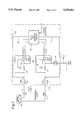
- FIG. 1is a schematic diagram illustrating basic components within the receive output stage 10 of a typical subscriber line interface circuit 11 that is fabricated on an integrated circuit.
- the receive output stage 10comprises a pair of operational amplifiers 12 and 14 configured as differential transconductance amplifiers.
- Such transconductance amplifiersgenerate an output current which is linearly dependent upon the differential input voltages applied thereto.
- the transconductance amplifierstypically provide a current gain of approximately 500. This current gain can be attained, for example, by selecting the resistance of a resistor 16 at 20 ohms and the resistance of a resistor 18 at 10 k ohms.
- the receive output stage 10is an integral portion of the SLIC circuitry known as the two-wire to four-wire converter. Other portions (not shown) of the two-wire to four-wire converter include a transmit amplifier and balance circuitry.
- the two-wire to four-wire converterinherently rejects longitudinal (common-mode) noise induced onto the subscriber loop from close proximity telephone and power cables. Additional suppression circuitry ensures that high-level longitudinal signals do not exceed the operating voltage range of the SLIC amplifiers.
- the operational amplifier 12drives a telephone subscriber loop tip line 15 through resistor 16 and the operational amplifier 14 drives a telephone subscriber loop ring line 17 through resistor 32.
- a telephone 20is shown connected to the tip and ring lines 15 and 17.
- the circuitis powered from ground to a battery voltage of -50 volts and operates around a predetermined quiescent point within the range defined by these voltage rails.
- An input and monitor circuit 25is shown coupled to the receive output stage 10.
- the input and monitor circuit 25receives voice signals through a system interface and correspondingly drives the receive output stage 10.
- the input and monitor circuit 25provides a variety of other functions, including amplification of transmit signals provided from telephone 20 through lines 26 and 27.
- Control circuityis further incorporated within the input and monitor circuit 25 to support other so-called BORSCHT functions (battery feed, overvoltage protection, ringing, supervision, coding, hybrid, and test) of the SLIC. Implementations of such SLIC circuity are described in detail in the literature of the known prior art, such as in the IEEE Journal of Solid State Circuits, Vol. SC-16, No. 4, August 1981, pp. 261-276.
- the DC current flowing through the subscriber loop when the telephone 20 is off-hookbe nominally 30-40 mA.
- This DC currentprovides power to the telephone circuitry such as a digital keypad.
- the impedance of the subscriber loopdepends upon the particular telephone connected to the loop as well as the transmission length of the loop. Typical values of loop resistance range between 0 to 2000 ohms.
- the SLICmust therefore be designed to provide the nominal DC current (I DC ) for this range of loop impedances while still allowing transmission of the AC voice signals.
- I DCnominal DC current
- One way of achieving thisis to maintain node X at a DC voltage of approximately -5 volts while regulating the current flowing through resistor 32 such that the loop current equals the nominal current of, say, 40 mA.
- Such a systemis known as an unbalanced system. It is noted that the input and monitor circuit 25 controls the operational amplifiers 12 and 14 to maintain the desired DC operating voltage and current. Depending upon the loop resistance, the DC voltage at node Y will be established at some operating point between -5 volts and the negative voltage rail of -50 volts. As represented by the waveforms at the tip and ring leads, a differential AC signal may be imposed upon the DC operating current to transmit voice signals.
- the power dissipated by the transistor drivers of operational amplifier 14 in this situationdepends upon the loop impedance.
- the power dissipated by the transistor drivers of operational amplifier 12is, on the other hand, relatively constant and low since a voltage at node X is fixed at only approximately -5 volts. Take for example the case where the loop impedance is 1000 ohms. If resistors 16 and 32 are each selected at 20 ohms and node X is regulated at a DC voltage of -5 volts, then a DC voltage of -45 volts is established at node Y when the nominal current of 40 mA flows through the loop.
- the loop impedanceis only 300 ohms when the nominal 40 mA current flows through loop, a voltage of -17 volts is established at node Y.
- the voltage drop across each of resistors 16 and 32is approximately 0.8 volts in either case.
- the power dissipated by the transistor drivers of operational amplifier 14can be approximated by the voltage drop between the output line of the amplifier and the -50 volt supply.
- the power dissipated by the driver transistors of operational amplifier 14is dependent upon the loop impedance.
- the amount of power dissipatedincreases dramatically as the loop impedance decreases.
- the pull-down driver transistor within the output stage of operational amplifier 14must sink a relatively large current when the loop impedance is low. This therefore requires that the driver transistor be relatively large and further results in increased heat generation within the integrated circuit when the loop impedance is low. This poses problems with the reliability of the integrated circuit and generally results in increased fabrication and packaging costs.
- a subscriber line interface circuitincludes an output stage having a pair of differential transconductance amplifiers to drive the tip and ring lines of a telephone exchange.
- the output stageincludes circuitry that advantageously reduces the power dissipated within the integrated circuit when the subscriber loop impedance is relatively low. As a result, heat generation within the integrated circuit is reduced. Circuit reliability may therefore be enhanced and fabrication and packaging costs may be reduced.
- an off-chip resistoris coupled from an output line of the ring line amplifier to the negative voltage rail. When the loop impedance is low, a relatively large voltage drop is established across the resistor which therefore absorbs a greater percentage of the loop current. Since the resistor is provided off-chip and diverts current that would otherwise flow through the ring-line amplifier, the overall heat dissipated within the integrated circuit is reduced.
- a subscriber line interface circuitcomprises an input circuit for receiving voice signals from a telephone exchange, a first output driver coupled to the input circuit for driving a tip line of a telephone subscriber loop and a second output driver coupled to the input circuit for driving a ring line of the telephone subscriber loop.
- the first and second output driversreceive power from a power supply having a first reference voltage terminal and a second reference voltage terminal.
- a resistoris coupled between the second reference voltage terminal and an output line of either the first or the second output driver.
- a subscriber line interface circuitcomprises an input circuit for receiving voice signals from a telephone exchange, a first operational amplifier coupled to the input circuit and including an output line for driving a tip line of a telephone subscriber loop and a second operational amplifier coupled to the input circuit and including an output line for driving a ring line of the telephone subscriber loop.
- the first and second operational amplifiersreceive power from a power supply having a first reference voltage terminal and a second reference voltage terminal and are configured to provide a regulated DC current through the ring and tip lines when a telephone subscriber is off-hook.
- a first resistoris coupled between the output line of the second operational amplifier and the second reference voltage terminal, a second resistor is coupled in series between the output line of the second operational amplifier and the ring line and a third resistor is coupled in series between the output line of the first operational amplifier and the tip line.
- FIG. 1is a schematic diagram illustrating basic components within a receive output stage of a typical subscriber line interface circuit fabricated on an integrated circuit.
- FIG. 2is a schematic diagram of an unbalanced subscriber line interface circuit that incorporates an off-chip resistor coupled to the ring-line amplifier for power management.
- FIG. 3is a schematic diagram of a balanced subscriber line interface circuit including a pair of off-chip resistors coupled to the ring-line and tip-line amplifiers for power management.
- FIG. 4is a schematic diagram of an additional embodiment of a subscriber line interface circuit.
- FIG. 2a schematic diagram is shown of an unbalanced subscriber line interface circuit 100 including a current sink resistor 102 and an electronic switch 104 coupled between the output line of the ring-line operational amplifier 14 and the -50 volt supply terminal.
- Resistor 102is provided externally from an integrated circuit chip that forms the remaining SLIC circuitry. Circuit components and elements that correspond to those of FIG. 1 are numbered identically. In this embodiment, resistor 102 is characterized with a resistance of 1000 ohms.
- a receive output stage 10comprises a pair of operational amplifiers 12 and 14 which are configured as differential transconductance amplifiers.
- the transconductance amplifiersprovide a current gain of 500.
- the input and monitor circuit 25maintains a DC operating voltage at node X of -5 volts and maintains the loop current I DC at a nominal value of 40 mA. It is noted that the input and monitor circuit 25 also provides AC voice signals to the transconductance amplifiers and may further accommodate a variety of other functions, such as BORSCHT functions (battery feed, over voltage protection, ringing, supervision, coding, hybrid, and test) of the SLIC. As stated previously, a variety of implementations of such input and monitor circuitry is described in detail in the literature of the known prior art.
- switch 104is closed and thus a current path is provided through resistor 102 between the output line of operational amplifier 14 and the -50 volt supply.
- the loop resistanceis 1000 ohms as considered above, the voltage at node Y is -45 volts.
- the loop resistanceis 300 ohms
- the voltage at node Yis -17 volts.
- resistor 102is coupled between resistor 32 and the output line of operational amplifier 14, the entire 40 mA of loop current flows through resistor 32. That is, the connection of resistor 102 does not affect the amount of current that flows through resistor 32. This characteristic is important since resistor 32 is used as a current sensing resistor to provide appropriate feedback signals to maintain the loop current at 40 mA.
- switch 104may be opened to eliminate the current path through resistor 102. This may be desirable when, for example, the subscriber line interface circuit is operated in alternative operating modes, such as test modes or to support coin-operated telephone systems. For instance, it may be desirable in some situations to open switch 104 and reverse the direction of the loop current.
- switch 104may be implemented using a switching transistor.
- switch 104could be eliminated such that resistor 102 would be directly-connected to the output line of operational amplifier 14.
- subscriber line interface circuitas shown in FIG. 2 may also be possible without departing from the spirit and scope of the invention.
- other input circuitry connected to the transconductance amplifiersmay be utilized, and lightening protection circuitry may be coupled in parallel with the subscriber loop.
- FIG. 3is a schematic diagram of a second embodiment of a subscriber line interface circuit.
- the circuit of FIG. 3is similar to that of FIG. 2 and corresponding components thereof are numbered identically.
- the subscriber line interface circuit of FIG. 3is a balanced system wherein the voltages at nodes X and Y vary symmetrically depending upon the subscriber loop impedance. In this embodiment, the voltage at node X may drop far below the -5 volt regulated value as described in conjunction with the unbalanced system of FIG. 2. Since this significantly increases the power dissipated by the driver transistors within operational amplifier 12, an off-chip resistor 106 is coupled through an electronic switch 110 between the output line of operational amplifier 12 and ground.
- a third electronic switch 112may be provided between the output line of operational amplifier 12 and resistor 102.
- a fourth electronic switch 118may be provided between the output line of operational amplifier 14 and resistor 106.
- switches 112 and 118are open and thus do not affect the current paths of the circuit.
- Switches 112 and 118may be closed and switches 104 and 110 may be opened to accommodate low on-chip power dissipation during alternative operating modes of the subscriber line interface circuit when the loop current is reversed. It is noted that switches 104, 110, 112 and 118 may be implemented using transistors.
- output stage 10 of the embodiments described aboveincludes a pair of transconductance amplifiers, a variety of other types of output drivers that drive the subscriber loop could be provided.
Landscapes
- Engineering & Computer Science (AREA)
- Power Engineering (AREA)
- Signal Processing (AREA)
- Interface Circuits In Exchanges (AREA)
- Amplifiers (AREA)
- Devices For Supply Of Signal Current (AREA)
Abstract
Description
Claims (42)
Priority Applications (4)
| Application Number | Priority Date | Filing Date | Title |
|---|---|---|---|
| US08/031,785US5428682A (en) | 1993-03-12 | 1993-03-12 | Subscriber line interface circuit with reduced on-chip power dissipation |
| DE69428068TDE69428068T2 (en) | 1993-03-12 | 1994-02-10 | Subscriber interface circuit |
| EP94300961AEP0615375B1 (en) | 1993-03-12 | 1994-02-10 | Subscriber line interface circuit |
| JP6038281AJPH06303655A (en) | 1993-03-12 | 1994-03-09 | Subscriber's circuit interface circuit |
Applications Claiming Priority (1)
| Application Number | Priority Date | Filing Date | Title |
|---|---|---|---|
| US08/031,785US5428682A (en) | 1993-03-12 | 1993-03-12 | Subscriber line interface circuit with reduced on-chip power dissipation |
Publications (1)
| Publication Number | Publication Date |
|---|---|
| US5428682Atrue US5428682A (en) | 1995-06-27 |
Family
ID=21861383
Family Applications (1)
| Application Number | Title | Priority Date | Filing Date |
|---|---|---|---|
| US08/031,785Expired - LifetimeUS5428682A (en) | 1993-03-12 | 1993-03-12 | Subscriber line interface circuit with reduced on-chip power dissipation |
Country Status (4)
| Country | Link |
|---|---|
| US (1) | US5428682A (en) |
| EP (1) | EP0615375B1 (en) |
| JP (1) | JPH06303655A (en) |
| DE (1) | DE69428068T2 (en) |
Cited By (52)
| Publication number | Priority date | Publication date | Assignee | Title |
|---|---|---|---|---|
| US5627833A (en)* | 1989-07-25 | 1997-05-06 | Raychem Corporation | Digital added main line system with power-up and power-down features |
| US5631548A (en)* | 1995-10-30 | 1997-05-20 | Motorola, Inc. | Power off-loading circuit and method for dissipating power |
| US5636274A (en)* | 1995-01-13 | 1997-06-03 | Harris Corp. | Switch controller and method |
| US5649009A (en)* | 1994-11-14 | 1997-07-15 | Harris Corporation | Differential longitudinal amplifier for a subscriber line interface circuit |
| US5737411A (en)* | 1994-12-29 | 1998-04-07 | Advanced Micro Devices Inc. | Battery switching in a telephone subscriber line interface circuit |
| WO1998021876A1 (en)* | 1996-11-08 | 1998-05-22 | Telefonaktiebolaget Lm Ericsson (Publ) | Power diverting device |
| US5870046A (en)* | 1997-04-22 | 1999-02-09 | Silicon Laboratories Inc. | Analog isolation system with digital communication across a capacitive barrier |
| US5909488A (en)* | 1995-08-22 | 1999-06-01 | Canon Kabushiki Kaisha | Communication apparatus having a non-ringing call receiving mode and an energy-saving stand-by mode |
| US5978390A (en)* | 1995-03-20 | 1999-11-02 | Raychem Corporation | Dual DDS data multiplexer |
| US5982878A (en)* | 1997-05-15 | 1999-11-09 | Hubbell Incorporated | Combined loop current sink, battery detector, and ringing detector circuit |
| US6104794A (en)* | 1997-04-22 | 2000-08-15 | Silicon Laboratories, Inc. | Architecture for minimum loop current during ringing and caller ID |
| US6115469A (en)* | 1998-08-25 | 2000-09-05 | Unitrode Corporation | Telephone line ring signal and DC power generator |
| US6137189A (en)* | 1999-07-30 | 2000-10-24 | Intersil Corporation | Line circuit apparatus for supplying power to a telephone set in telecommunication systems |
| US6137827A (en)* | 1997-04-22 | 2000-10-24 | Silicon Laboratories, Inc. | Isolation system with digital communication across a capacitive barrier |
| US6160885A (en)* | 1997-04-22 | 2000-12-12 | Silicon Laboratories, Inc. | Caller ID circuit powered through hookswitch devices |
| US6167134A (en)* | 1997-04-22 | 2000-12-26 | Silicon Laboratories, Inc. | External resistor and method to minimize power dissipation in DC holding circuitry for a communication system |
| US6167132A (en)* | 1997-04-22 | 2000-12-26 | Silicon Laboratories, Inc. | Analog successive approximation (SAR) analog-to-digital converter (ADC) |
| US6201865B1 (en) | 1997-04-22 | 2001-03-13 | Silicon Laboratories, Inc. | Digital access arrangement circuitry and method for connecting to phone lines having a DC holding circuit with switchable time constants |
| US6222922B1 (en) | 1997-04-22 | 2001-04-24 | Silicon Laboratories, Inc. | Loop current monitor circuitry and method for a communication system |
| US6249109B1 (en)* | 2000-03-21 | 2001-06-19 | Nokia Mobile Phones Limited | Heat transfer from active high drop regulator |
| US6282204B1 (en) | 1997-12-19 | 2001-08-28 | Terayon Communication Systems, Inc. | ISDN plus voice multiplexer system |
| US6289070B1 (en) | 1997-04-22 | 2001-09-11 | Silicon Laboratories, Inc. | Digital isolation system with ADC offset calibration including coarse offset |
| US6298133B1 (en) | 1997-04-22 | 2001-10-02 | Silicon Laboratories, Inc. | Telephone line interface architecture using ringer inputs for caller ID data |
| US6307891B1 (en) | 1997-04-22 | 2001-10-23 | Silicon Laboratories, Inc. | Method and apparatus for freezing a communication link during a disruptive event |
| US6323796B1 (en) | 1997-04-22 | 2001-11-27 | Silicon Laboratories, Inc. | Digital isolation system with ADC offset calibration |
| US6356624B1 (en)* | 1998-08-04 | 2002-03-12 | Leserity, Inc. | Method and apparatus for detecting and measuring foreign voltages |
| US6377681B1 (en)* | 1998-04-01 | 2002-04-23 | National Semiconductor Corporation | Signal line driving circuit with self-controlled power dissipation |
| US6385235B1 (en) | 1997-04-22 | 2002-05-07 | Silicon Laboratories, Inc. | Direct digital access arrangement circuitry and method for connecting to phone lines |
| US6408034B1 (en) | 1997-04-22 | 2002-06-18 | Silicon Laboratories, Inc. | Framed delta sigma data with unlikely delta sigma data patterns |
| US6430229B1 (en) | 1997-04-22 | 2002-08-06 | Silicon Laboratories Inc. | Capacitive isolation system with digital communication and power transfer |
| US6442213B1 (en) | 1997-04-22 | 2002-08-27 | Silicon Laboratories Inc. | Digital isolation system with hybrid circuit in ADC calibration loop |
| US6442271B1 (en) | 1997-04-22 | 2002-08-27 | Silicon Laboratories, Inc. | Digital isolation system with low power mode |
| US6456712B1 (en) | 1997-04-22 | 2002-09-24 | Silicon Laboratories Inc. | Separation of ring detection functions across isolation barrier for minimum power |
| US6498825B1 (en) | 1997-04-22 | 2002-12-24 | Silicon Laboratories Inc. | Digital access arrangement circuitry and method for connecting to phone lines having a DC holding circuit with programmable current limiting |
| US6516024B1 (en) | 1997-04-22 | 2003-02-04 | Silicon Laboratories Inc. | Digital access arrangement circuitry and method for connecting to phone lines having a DC holding circuit with low distortion and current limiting |
| US6522745B1 (en) | 1997-04-22 | 2003-02-18 | Silicon Laboratories Inc. | Digital access arrangement circuitry and method having a synthesized ringer impedance for connecting to phone lines |
| US20030169874A1 (en)* | 2002-03-06 | 2003-09-11 | Intersil Americas Inc. | Enhanced high voltage interface for partitioned subscriber line interface circuit |
| US20030194083A1 (en)* | 1997-04-22 | 2003-10-16 | Scott Jeffrey W. | Separation of ring detection functions across isolation barrier for minimum power |
| US6678377B1 (en)* | 1998-12-31 | 2004-01-13 | Stmicroelectronics S.R.L. | Monolithically integrated telephone circuit for driving wide-band telephone lines for data transmission |
| US20040120512A1 (en)* | 2002-12-20 | 2004-06-24 | Ploumen Franciscus Maria | System and method for optimizing power dissipation in subscriber interface line circuits (SLICS) |
| US20040151305A1 (en)* | 2003-01-30 | 2004-08-05 | Serconet Ltd | Method and system for providing DC power on local telephone lines |
| US20040247108A1 (en)* | 1997-04-22 | 2004-12-09 | Silicon Laboratories Inc. | Digital access arrangement circuitry and method having current ramping control of the hookswitch |
| US20050036604A1 (en)* | 1997-04-22 | 2005-02-17 | Silicon Laboratories Inc. | Direct digital access arrangement circuitry and method for connecting DSL circuitry to phone lines |
| US20060002219A1 (en)* | 2004-06-30 | 2006-01-05 | George Scott A | Power offloading for a subscriber line interface circuit |
| US20060002545A1 (en)* | 2004-06-30 | 2006-01-05 | George Scott A | Power offloading for a subscriber line interface circuit |
| US7158633B1 (en)* | 1999-11-16 | 2007-01-02 | Silicon Laboratories, Inc. | Method and apparatus for monitoring subscriber loop interface circuitry power dissipation |
| US7424031B2 (en) | 1998-07-28 | 2008-09-09 | Serconet, Ltd. | Local area network of serial intelligent cells |
| US7483524B2 (en) | 1999-07-20 | 2009-01-27 | Serconet, Ltd | Network for telephony and data communication |
| US7522714B2 (en) | 2000-03-20 | 2009-04-21 | Serconet Ltd. | Telephone outlet for implementing a local area network over telephone lines and a local area network using such outlets |
| US8582598B2 (en) | 1999-07-07 | 2013-11-12 | Mosaid Technologies Incorporated | Local area network for distributing data communication, sensing and control signals |
| KR20180084290A (en)* | 2017-01-16 | 2018-07-25 | 주식회사 실리콘웍스 | Thermal dispersion circuit and regulator control circuit |
| US10986164B2 (en) | 2004-01-13 | 2021-04-20 | May Patents Ltd. | Information device |
Families Citing this family (4)
| Publication number | Priority date | Publication date | Assignee | Title |
|---|---|---|---|---|
| JP2760325B2 (en)* | 1995-09-22 | 1998-05-28 | 日本電気株式会社 | Subscriber circuit |
| US6480603B1 (en)* | 1998-11-06 | 2002-11-12 | Nortel Networks Limited | Device which reduces central office battery current during modem connections |
| US6760380B1 (en) | 1998-12-07 | 2004-07-06 | Lynk Labs, Inc. | Data transmission apparatus and method |
| JP3768776B2 (en)* | 2000-04-28 | 2006-04-19 | 株式会社ルネサステクノロジ | Line interface circuit and information communication apparatus using the same |
Citations (5)
| Publication number | Priority date | Publication date | Assignee | Title |
|---|---|---|---|---|
| US4677667A (en)* | 1985-08-29 | 1987-06-30 | Gte Communication Systems Corporation | Subscriber line circuit having improved AC impedance matching |
| US4677669A (en)* | 1984-05-30 | 1987-06-30 | Fujitsu Limited | Battery feed circuit for a pair of subscriber lines |
| US4866768A (en)* | 1985-06-26 | 1989-09-12 | Siemens Corporate Research & Support, Inc. | Station line interface circuit for a telecommunication network |
| US4879746A (en)* | 1987-12-30 | 1989-11-07 | Plantronics, Inc. | Voice communication link interface apparatus |
| US5046089A (en)* | 1988-10-31 | 1991-09-03 | Sgs-Thomson Microelectronics S.R.L. | Subscriber line interface circuit with power-down mode |
Family Cites Families (1)
| Publication number | Priority date | Publication date | Assignee | Title |
|---|---|---|---|---|
| IT1244074B (en)* | 1990-10-24 | 1994-07-05 | Sgs Thomson Microelectronics | PROTECTION DEVICE FOR ELECTRICAL AND / OR ELECTRONIC CIRCUITS OF TELEPHONES SUITABLE TO LIMIT THE POWER DISSIPATED IN THEM. |
- 1993
- 1993-03-12USUS08/031,785patent/US5428682A/ennot_activeExpired - Lifetime
- 1994
- 1994-02-10DEDE69428068Tpatent/DE69428068T2/ennot_activeExpired - Lifetime
- 1994-02-10EPEP94300961Apatent/EP0615375B1/ennot_activeExpired - Lifetime
- 1994-03-09JPJP6038281Apatent/JPH06303655A/ennot_activeWithdrawn
Patent Citations (5)
| Publication number | Priority date | Publication date | Assignee | Title |
|---|---|---|---|---|
| US4677669A (en)* | 1984-05-30 | 1987-06-30 | Fujitsu Limited | Battery feed circuit for a pair of subscriber lines |
| US4866768A (en)* | 1985-06-26 | 1989-09-12 | Siemens Corporate Research & Support, Inc. | Station line interface circuit for a telecommunication network |
| US4677667A (en)* | 1985-08-29 | 1987-06-30 | Gte Communication Systems Corporation | Subscriber line circuit having improved AC impedance matching |
| US4879746A (en)* | 1987-12-30 | 1989-11-07 | Plantronics, Inc. | Voice communication link interface apparatus |
| US5046089A (en)* | 1988-10-31 | 1991-09-03 | Sgs-Thomson Microelectronics S.R.L. | Subscriber line interface circuit with power-down mode |
Non-Patent Citations (4)
| Title |
|---|
| Electronic Design, Jul. 11, 1994 vol. 42, No. 14, article entitled "High-Voltage Bonded-Wafer ICs Create First SLIC to Switch The 93-V RMS Phone-Line Ring Voltage on-Chip, Eliminating PABX Relays", written by Frank Goodenough, pp. 55-64, Cover Page, Table of Contents. |
| Electronic Design, Jul. 11, 1994 vol. 42, No. 14, article entitled High Voltage Bonded Wafer ICs Create First SLIC to Switch The 93 V RMS Phone Line Ring Voltage on Chip, Eliminating PABX Relays , written by Frank Goodenough, pp. 55 64, Cover Page, Table of Contents.* |
| HC 5506 Specification for Dual Subscriber Line Interface Circuit (DSLIC), Harris Semiconductor, Advance Information, Jun. 1994, 16 pages.* |
| HC-5506 Specification for Dual Subscriber Line Interface Circuit (DSLIC), Harris Semiconductor, Advance Information, Jun. 1994, 16 pages. |
Cited By (122)
| Publication number | Priority date | Publication date | Assignee | Title |
|---|---|---|---|---|
| US5627833A (en)* | 1989-07-25 | 1997-05-06 | Raychem Corporation | Digital added main line system with power-up and power-down features |
| US5649009A (en)* | 1994-11-14 | 1997-07-15 | Harris Corporation | Differential longitudinal amplifier for a subscriber line interface circuit |
| US5737411A (en)* | 1994-12-29 | 1998-04-07 | Advanced Micro Devices Inc. | Battery switching in a telephone subscriber line interface circuit |
| US5636274A (en)* | 1995-01-13 | 1997-06-03 | Harris Corp. | Switch controller and method |
| US5978390A (en)* | 1995-03-20 | 1999-11-02 | Raychem Corporation | Dual DDS data multiplexer |
| US5909488A (en)* | 1995-08-22 | 1999-06-01 | Canon Kabushiki Kaisha | Communication apparatus having a non-ringing call receiving mode and an energy-saving stand-by mode |
| US5631548A (en)* | 1995-10-30 | 1997-05-20 | Motorola, Inc. | Power off-loading circuit and method for dissipating power |
| US6239648B1 (en)* | 1996-11-08 | 2001-05-29 | Telefonaktiebolaget Lm Ericsson (Publ) | System and method for dissipating heat in an electric device |
| WO1998021876A1 (en)* | 1996-11-08 | 1998-05-22 | Telefonaktiebolaget Lm Ericsson (Publ) | Power diverting device |
| US6975723B2 (en) | 1997-04-22 | 2005-12-13 | Silicon Laboratories Inc. | Architecture for minimum loop current during ringing and caller ID |
| US6959083B2 (en) | 1997-04-22 | 2005-10-25 | Silicon Laboratories Inc. | Loop current monitor circuitry and method for a communication system |
| US6107948A (en)* | 1997-04-22 | 2000-08-22 | Silicon Laboratories, Inc. | Analog isolation system with digital communication across a capacitive barrier |
| US7515672B2 (en) | 1997-04-22 | 2009-04-07 | Silicon Laboratories Inc. | Digital access arrangement circuitry and method for connecting to phone lines having a DC holding circuit with programmable current limiting |
| US5870046A (en)* | 1997-04-22 | 1999-02-09 | Silicon Laboratories Inc. | Analog isolation system with digital communication across a capacitive barrier |
| US6137827A (en)* | 1997-04-22 | 2000-10-24 | Silicon Laboratories, Inc. | Isolation system with digital communication across a capacitive barrier |
| US6160885A (en)* | 1997-04-22 | 2000-12-12 | Silicon Laboratories, Inc. | Caller ID circuit powered through hookswitch devices |
| US6167134A (en)* | 1997-04-22 | 2000-12-26 | Silicon Laboratories, Inc. | External resistor and method to minimize power dissipation in DC holding circuitry for a communication system |
| US6167132A (en)* | 1997-04-22 | 2000-12-26 | Silicon Laboratories, Inc. | Analog successive approximation (SAR) analog-to-digital converter (ADC) |
| US6191717B1 (en) | 1997-04-22 | 2001-02-20 | Silicon Laboratories Inc. | Analog isolation system with digital communication across a capactive barrier |
| US6201865B1 (en) | 1997-04-22 | 2001-03-13 | Silicon Laboratories, Inc. | Digital access arrangement circuitry and method for connecting to phone lines having a DC holding circuit with switchable time constants |
| US6222922B1 (en) | 1997-04-22 | 2001-04-24 | Silicon Laboratories, Inc. | Loop current monitor circuitry and method for a communication system |
| US6225927B1 (en) | 1997-04-22 | 2001-05-01 | Silicon Laboratories, Inc. | Analog isolation system with digital communication across a capacitive barrier |
| US7463675B2 (en) | 1997-04-22 | 2008-12-09 | Silicon Laboratories Inc. | Direct digital access arrangement circuitry and method for connecting to phone lines |
| US7362841B2 (en) | 1997-04-22 | 2008-04-22 | Silicon Laboratories Inc. | Digital access arrangement circuitry and method for connecting to phone lines having a DC holding circuit with switchable DC termination impedance |
| US7301995B2 (en) | 1997-04-22 | 2007-11-27 | Silicon Laboratories Inc. | Direct digital access arrangement circuitry and method for connecting to phone lines |
| US6289070B1 (en) | 1997-04-22 | 2001-09-11 | Silicon Laboratories, Inc. | Digital isolation system with ADC offset calibration including coarse offset |
| US6298133B1 (en) | 1997-04-22 | 2001-10-02 | Silicon Laboratories, Inc. | Telephone line interface architecture using ringer inputs for caller ID data |
| US6297755B2 (en) | 1997-04-22 | 2001-10-02 | Silicon Laboratories, Inc. | Analog isolation system with digital communication across a capacitive barrier |
| US6307891B1 (en) | 1997-04-22 | 2001-10-23 | Silicon Laboratories, Inc. | Method and apparatus for freezing a communication link during a disruptive event |
| US20030194083A1 (en)* | 1997-04-22 | 2003-10-16 | Scott Jeffrey W. | Separation of ring detection functions across isolation barrier for minimum power |
| US6330330B2 (en) | 1997-04-22 | 2001-12-11 | Silicon Laboratories, Inc. | External resistor and method to minimize power dissipation in DC holding circuitry for a communication system |
| US7283584B2 (en) | 1997-04-22 | 2007-10-16 | Silicon Laboratories Inc. | Direct digital access arrangement circuitry and method for connecting to phone lines |
| US7203224B2 (en) | 1997-04-22 | 2007-04-10 | Silicon Laboratories | Isolation system with digital communication across a capacitive barrier |
| US6385235B1 (en) | 1997-04-22 | 2002-05-07 | Silicon Laboratories, Inc. | Direct digital access arrangement circuitry and method for connecting to phone lines |
| US6654409B1 (en) | 1997-04-22 | 2003-11-25 | Silicon Laboratories, Inc. | Direct digital access arrangement circuitry and method for connecting DSL circuitry to phone lines |
| US6408034B1 (en) | 1997-04-22 | 2002-06-18 | Silicon Laboratories, Inc. | Framed delta sigma data with unlikely delta sigma data patterns |
| US6430229B1 (en) | 1997-04-22 | 2002-08-06 | Silicon Laboratories Inc. | Capacitive isolation system with digital communication and power transfer |
| US6442213B1 (en) | 1997-04-22 | 2002-08-27 | Silicon Laboratories Inc. | Digital isolation system with hybrid circuit in ADC calibration loop |
| US6442271B1 (en) | 1997-04-22 | 2002-08-27 | Silicon Laboratories, Inc. | Digital isolation system with low power mode |
| US6456712B1 (en) | 1997-04-22 | 2002-09-24 | Silicon Laboratories Inc. | Separation of ring detection functions across isolation barrier for minimum power |
| US20020154702A1 (en)* | 1997-04-22 | 2002-10-24 | Silicon Laboratories Inc. | Direct digital access arrangement circuitry and method for connecting to phone lines |
| US6498825B1 (en) | 1997-04-22 | 2002-12-24 | Silicon Laboratories Inc. | Digital access arrangement circuitry and method for connecting to phone lines having a DC holding circuit with programmable current limiting |
| US20030002571A1 (en)* | 1997-04-22 | 2003-01-02 | Silicon Laboratories Inc. | Direct digital access arrangement circuitry and method for connecting to phone lines |
| US6516024B1 (en) | 1997-04-22 | 2003-02-04 | Silicon Laboratories Inc. | Digital access arrangement circuitry and method for connecting to phone lines having a DC holding circuit with low distortion and current limiting |
| US6522745B1 (en) | 1997-04-22 | 2003-02-18 | Silicon Laboratories Inc. | Digital access arrangement circuitry and method having a synthesized ringer impedance for connecting to phone lines |
| US20030091140A1 (en)* | 1997-04-22 | 2003-05-15 | Silicon Laboratories Inc. | Digital access arrangment circuitry and method for connecting to phone lines having a DC holding circuit with switchable DC termination impedance |
| US6570513B2 (en) | 1997-04-22 | 2003-05-27 | Silicon Laboratories Inc. | Isolation system with digital communication across a capacitive barrier |
| US6611553B1 (en) | 1997-04-22 | 2003-08-26 | Silicon Laboratories Inc. | Isolation system with digital communication across a capacitive barrier |
| US7200167B2 (en) | 1997-04-22 | 2007-04-03 | Silicon Laboratories Inc. | Direct digital access arrangement circuitry and method for connecting to phone lines |
| US6323796B1 (en) | 1997-04-22 | 2001-11-27 | Silicon Laboratories, Inc. | Digital isolation system with ADC offset calibration |
| US6104794A (en)* | 1997-04-22 | 2000-08-15 | Silicon Laboratories, Inc. | Architecture for minimum loop current during ringing and caller ID |
| US6389061B1 (en) | 1997-04-22 | 2002-05-14 | Silicon Laboratories Inc. | Isolation system with digital communication across a capacitive barrier |
| US7154940B2 (en) | 1997-04-22 | 2006-12-26 | Silicon Laboratories Inc. | Isolation system with digital communication across a capacitive barrier |
| US6683548B2 (en) | 1997-04-22 | 2004-01-27 | Silicon Laboratories Inc. | Analog isolation system with digital communication across a capacitive barrier |
| US20040057524A1 (en)* | 1997-04-22 | 2004-03-25 | Silicon Laboratories Inc. | Digital isolation system with ADC offset calibration |
| US20040081232A1 (en)* | 1997-04-22 | 2004-04-29 | Silicon Laboratories Inc. | Isolation system with digital communication across a capacitive barrier |
| US20040091100A1 (en)* | 1997-04-22 | 2004-05-13 | Silicon Laboratories Inc. | Loop current monitor circuitry and method for a communication system |
| US20040101132A1 (en)* | 1997-04-22 | 2004-05-27 | Silicon Laboratories Inc. | Analog isolation system with digital communication across a capacitive barrier |
| US6754341B2 (en)* | 1997-04-22 | 2004-06-22 | Silicon Laboratories, Inc. | External resistor and method to minimize power dissipation in DC holding circuitry for a communication system |
| US7072389B2 (en) | 1997-04-22 | 2006-07-04 | Silicon Laboratories Inc. | Direct digital access arrangement circuitry and method for connecting to phone lines |
| US7050509B2 (en) | 1997-04-22 | 2006-05-23 | Silicon Laboratories Inc. | Digital isolation system with hybrid circuit in ADC calibration loop |
| US20040161024A1 (en)* | 1997-04-22 | 2004-08-19 | Silicon Laboratories, Inc. | Direct digital access arrangement circuitry and method for connecting to phone lines |
| US20040190670A1 (en)* | 1997-04-22 | 2004-09-30 | Silicon Laboratories Inc. | Digital access arrangement circuitry and method for connecting to phone lines having a DC holding circuit with switchable time constants |
| US20040228475A1 (en)* | 1997-04-22 | 2004-11-18 | Silicon Laboratories Inc. | External resistor and method to minimize power dissipation in DC holding circuitry for a communication system |
| US20040247108A1 (en)* | 1997-04-22 | 2004-12-09 | Silicon Laboratories Inc. | Digital access arrangement circuitry and method having current ramping control of the hookswitch |
| US20050036604A1 (en)* | 1997-04-22 | 2005-02-17 | Silicon Laboratories Inc. | Direct digital access arrangement circuitry and method for connecting DSL circuitry to phone lines |
| US20050100104A1 (en)* | 1997-04-22 | 2005-05-12 | Silicon Laboratories Inc. | Digital access arrangement circuitry and method for connecting to phone lines having a DC holding circuit with programmable current limiting |
| US6922469B2 (en) | 1997-04-22 | 2005-07-26 | Silicon Laboratories, Inc. | Separation of ring detection functions across isolation barrier for minimum power |
| US20030206626A1 (en)* | 1997-04-22 | 2003-11-06 | Scott Jeffrey W. | Low voltage circuits powered by the phone line |
| US7046793B2 (en) | 1997-04-22 | 2006-05-16 | Silicon Laboratories Inc. | Digital access arrangement circuitry and method having current ramping control of the hookswitch |
| US7046755B2 (en) | 1997-04-22 | 2006-05-16 | Silicon Laboratories Inc. | Digital access arrangement circuitry and method for connecting to phone lines having a DC holding circuit with switchable time constants |
| US7003023B2 (en) | 1997-04-22 | 2006-02-21 | Silicon Laboratories Inc. | Digital isolation system with ADC offset calibration |
| US5982878A (en)* | 1997-05-15 | 1999-11-09 | Hubbell Incorporated | Combined loop current sink, battery detector, and ringing detector circuit |
| US6282204B1 (en) | 1997-12-19 | 2001-08-28 | Terayon Communication Systems, Inc. | ISDN plus voice multiplexer system |
| US6377681B1 (en)* | 1998-04-01 | 2002-04-23 | National Semiconductor Corporation | Signal line driving circuit with self-controlled power dissipation |
| US8885660B2 (en) | 1998-07-28 | 2014-11-11 | Conversant Intellectual Property Management Incorporated | Local area network of serial intelligent cells |
| US7424031B2 (en) | 1998-07-28 | 2008-09-09 | Serconet, Ltd. | Local area network of serial intelligent cells |
| US7830858B2 (en) | 1998-07-28 | 2010-11-09 | Mosaid Technologies Incorporated | Local area network of serial intelligent cells |
| US7986708B2 (en) | 1998-07-28 | 2011-07-26 | Mosaid Technologies Incorporated | Local area network of serial intelligent cells |
| US7978726B2 (en) | 1998-07-28 | 2011-07-12 | Mosaid Technologies Incorporated | Local area network of serial intelligent cells |
| US7965735B2 (en) | 1998-07-28 | 2011-06-21 | Mosaid Technologies Incorporated | Local area network of serial intelligent cells |
| US8270430B2 (en) | 1998-07-28 | 2012-09-18 | Mosaid Technologies Incorporated | Local area network of serial intelligent cells |
| US8908673B2 (en) | 1998-07-28 | 2014-12-09 | Conversant Intellectual Property Management Incorporated | Local area network of serial intelligent cells |
| US7969917B2 (en) | 1998-07-28 | 2011-06-28 | Mosaid Technologies Incorporated | Local area network of serial intelligent cells |
| US8325636B2 (en) | 1998-07-28 | 2012-12-04 | Mosaid Technologies Incorporated | Local area network of serial intelligent cells |
| US7653015B2 (en) | 1998-07-28 | 2010-01-26 | Mosaid Technologies Incorporated | Local area network of serial intelligent cells |
| US7852874B2 (en) | 1998-07-28 | 2010-12-14 | Mosaid Technologies Incorporated | Local area network of serial intelligent cells |
| US8885659B2 (en) | 1998-07-28 | 2014-11-11 | Conversant Intellectual Property Management Incorporated | Local area network of serial intelligent cells |
| US8867523B2 (en) | 1998-07-28 | 2014-10-21 | Conversant Intellectual Property Management Incorporated | Local area network of serial intelligent cells |
| US6356624B1 (en)* | 1998-08-04 | 2002-03-12 | Leserity, Inc. | Method and apparatus for detecting and measuring foreign voltages |
| US6115469A (en)* | 1998-08-25 | 2000-09-05 | Unitrode Corporation | Telephone line ring signal and DC power generator |
| US6678377B1 (en)* | 1998-12-31 | 2004-01-13 | Stmicroelectronics S.R.L. | Monolithically integrated telephone circuit for driving wide-band telephone lines for data transmission |
| US8582598B2 (en) | 1999-07-07 | 2013-11-12 | Mosaid Technologies Incorporated | Local area network for distributing data communication, sensing and control signals |
| US7483524B2 (en) | 1999-07-20 | 2009-01-27 | Serconet, Ltd | Network for telephony and data communication |
| US8929523B2 (en) | 1999-07-20 | 2015-01-06 | Conversant Intellectual Property Management Inc. | Network for telephony and data communication |
| US7522713B2 (en) | 1999-07-20 | 2009-04-21 | Serconet, Ltd. | Network for telephony and data communication |
| US7492875B2 (en) | 1999-07-20 | 2009-02-17 | Serconet, Ltd. | Network for telephony and data communication |
| US8351582B2 (en) | 1999-07-20 | 2013-01-08 | Mosaid Technologies Incorporated | Network for telephony and data communication |
| US6137189A (en)* | 1999-07-30 | 2000-10-24 | Intersil Corporation | Line circuit apparatus for supplying power to a telephone set in telecommunication systems |
| US7158633B1 (en)* | 1999-11-16 | 2007-01-02 | Silicon Laboratories, Inc. | Method and apparatus for monitoring subscriber loop interface circuitry power dissipation |
| US8363797B2 (en) | 2000-03-20 | 2013-01-29 | Mosaid Technologies Incorporated | Telephone outlet for implementing a local area network over telephone lines and a local area network using such outlets |
| US7522714B2 (en) | 2000-03-20 | 2009-04-21 | Serconet Ltd. | Telephone outlet for implementing a local area network over telephone lines and a local area network using such outlets |
| US8855277B2 (en) | 2000-03-20 | 2014-10-07 | Conversant Intellectual Property Managment Incorporated | Telephone outlet for implementing a local area network over telephone lines and a local area network using such outlets |
| US7715534B2 (en) | 2000-03-20 | 2010-05-11 | Mosaid Technologies Incorporated | Telephone outlet for implementing a local area network over telephone lines and a local area network using such outlets |
| US6249109B1 (en)* | 2000-03-21 | 2001-06-19 | Nokia Mobile Phones Limited | Heat transfer from active high drop regulator |
| US7206405B2 (en)* | 2002-03-06 | 2007-04-17 | Intersil Americas Inc. | Enhanced high voltage interface for partitioned subscriber line interface circuit |
| US20030169874A1 (en)* | 2002-03-06 | 2003-09-11 | Intersil Americas Inc. | Enhanced high voltage interface for partitioned subscriber line interface circuit |
| US20040120512A1 (en)* | 2002-12-20 | 2004-06-24 | Ploumen Franciscus Maria | System and method for optimizing power dissipation in subscriber interface line circuits (SLICS) |
| US7317793B2 (en)* | 2003-01-30 | 2008-01-08 | Serconet Ltd | Method and system for providing DC power on local telephone lines |
| US8107618B2 (en) | 2003-01-30 | 2012-01-31 | Mosaid Technologies Incorporated | Method and system for providing DC power on local telephone lines |
| US20040151305A1 (en)* | 2003-01-30 | 2004-08-05 | Serconet Ltd | Method and system for providing DC power on local telephone lines |
| US8787562B2 (en) | 2003-01-30 | 2014-07-22 | Conversant Intellectual Property Management Inc. | Method and system for providing DC power on local telephone lines |
| US7702095B2 (en) | 2003-01-30 | 2010-04-20 | Mosaid Technologies Incorporated | Method and system for providing DC power on local telephone lines |
| US10986164B2 (en) | 2004-01-13 | 2021-04-20 | May Patents Ltd. | Information device |
| US11095708B2 (en) | 2004-01-13 | 2021-08-17 | May Patents Ltd. | Information device |
| US11032353B2 (en) | 2004-01-13 | 2021-06-08 | May Patents Ltd. | Information device |
| US7155008B2 (en)* | 2004-06-30 | 2006-12-26 | Silicon Laboratories, Inc. | Power offloading for a subscriber line interface circuit |
| US7164763B2 (en)* | 2004-06-30 | 2007-01-16 | Silicon Laboratories, Inc. | Power offloading for a subscriber line interface circuit |
| US20060002219A1 (en)* | 2004-06-30 | 2006-01-05 | George Scott A | Power offloading for a subscriber line interface circuit |
| US20060002545A1 (en)* | 2004-06-30 | 2006-01-05 | George Scott A | Power offloading for a subscriber line interface circuit |
| KR20180084290A (en)* | 2017-01-16 | 2018-07-25 | 주식회사 실리콘웍스 | Thermal dispersion circuit and regulator control circuit |
| US10437276B2 (en)* | 2017-01-16 | 2019-10-08 | Silicon Works Co., Ltd. | Heat dissipation circuit and regulator control circuit including the same |
Also Published As
| Publication number | Publication date |
|---|---|
| EP0615375A2 (en) | 1994-09-14 |
| EP0615375A3 (en) | 1998-04-01 |
| EP0615375B1 (en) | 2001-08-29 |
| DE69428068D1 (en) | 2001-10-04 |
| DE69428068T2 (en) | 2002-04-18 |
| JPH06303655A (en) | 1994-10-28 |
Similar Documents
| Publication | Publication Date | Title |
|---|---|---|
| US5428682A (en) | Subscriber line interface circuit with reduced on-chip power dissipation | |
| US4476350A (en) | Battery feed circuit | |
| US5737411A (en) | Battery switching in a telephone subscriber line interface circuit | |
| EP0212632B1 (en) | Subscriber line interface circuit | |
| US6674845B2 (en) | Method and apparatus for connecting broadband voice and data signals to telephone systems | |
| CA1292588C (en) | Subscriber line interface circuit | |
| US5596637A (en) | Power dissipation manager circuit for an interface device feeding a subscriber telephone line | |
| US4961219A (en) | Circuit for synthesizing an impedance across the tip and ring leads of a telephone line circuit | |
| GB2093314A (en) | Battery Feed Circuit | |
| US20100124326A1 (en) | Subscriber line interface circuitry with common base audio isolation stage | |
| JPH05145627A (en) | Ring trip detection circuit | |
| US6377681B1 (en) | Signal line driving circuit with self-controlled power dissipation | |
| KR100293948B1 (en) | subscriber interface circuit of electronic exchange system | |
| CA1157978A (en) | Loop sensing circuit for use with a subscriber loop interface circuit | |
| US6563924B1 (en) | Subscriber matching circuit for electronic exchange | |
| KR940011281B1 (en) | Constant voltage drive type driver circuit | |
| US5172412A (en) | Subscriber circuit capable of suppressing in-phase induced noise | |
| US5347575A (en) | Circuit to detect the hook status and ringing at the CPE end of a telephone network | |
| US20050220293A1 (en) | Subscriber loop interface circuitry with tracking battery supply | |
| US20050220291A1 (en) | Low voltage sensing and control of battery referenced transistors in subscriber loop applications | |
| US7206405B2 (en) | Enhanced high voltage interface for partitioned subscriber line interface circuit | |
| JPS6333755B2 (en) | ||
| KR100391885B1 (en) | Subscriber interface circuit of full electronic switching system | |
| JPS6188695A (en) | Low-resistance transmitting scanning circuit | |
| JP3506005B2 (en) | Telephone network subscriber circuit |
Legal Events
| Date | Code | Title | Description |
|---|---|---|---|
| STPP | Information on status: patent application and granting procedure in general | Free format text:APPLICATION UNDERGOING PREEXAM PROCESSING | |
| AS | Assignment | Owner name:ADVANCED MICRO DEVICES, INC., CALIFORNIA Free format text:ASSIGNMENT OF ASSIGNORS INTEREST.;ASSIGNOR:APFEL, RUSSELL J.;REEL/FRAME:006509/0166 Effective date:19930311 | |
| FEPP | Fee payment procedure | Free format text:PAYOR NUMBER ASSIGNED (ORIGINAL EVENT CODE: ASPN); ENTITY STATUS OF PATENT OWNER: LARGE ENTITY | |
| FPAY | Fee payment | Year of fee payment:4 | |
| AS | Assignment | Owner name:MORGAN STANLEY & CO. INCORPORATED, NEW YORK Free format text:SECURITY INTEREST;ASSIGNOR:LEGERITY, INC.;REEL/FRAME:011601/0539 Effective date:20000804 | |
| AS | Assignment | Owner name:LEGERITY, INC., TEXAS Free format text:ASSIGNMENT OF ASSIGNORS INTEREST;ASSIGNOR:ADVANCED MICRO DEVICES, INC.;REEL/FRAME:011700/0686 Effective date:20000731 | |
| FPAY | Fee payment | Year of fee payment:8 | |
| AS | Assignment | Owner name:MORGAN STANLEY & CO. INCORPORATED, AS FACILITY COL Free format text:SECURITY AGREEMENT;ASSIGNORS:LEGERITY, INC.;LEGERITY HOLDINGS, INC.;LEGERITY INTERNATIONAL, INC.;REEL/FRAME:013372/0063 Effective date:20020930 | |
| FEPP | Fee payment procedure | Free format text:PAYOR NUMBER ASSIGNED (ORIGINAL EVENT CODE: ASPN); ENTITY STATUS OF PATENT OWNER: LARGE ENTITY Free format text:PAYER NUMBER DE-ASSIGNED (ORIGINAL EVENT CODE: RMPN); ENTITY STATUS OF PATENT OWNER: LARGE ENTITY | |
| FPAY | Fee payment | Year of fee payment:12 | |
| AS | Assignment | Owner name:LEGERITY, INC., TEXAS Free format text:RELEASE BY SECURED PARTY;ASSIGNOR:MORGAN STANLEY SENIOR FUNDING INC;REEL/FRAME:019640/0676 Effective date:20070803 Owner name:LEGERITY, INC.,TEXAS Free format text:RELEASE BY SECURED PARTY;ASSIGNOR:MORGAN STANLEY SENIOR FUNDING INC;REEL/FRAME:019640/0676 Effective date:20070803 |