US5428314A - Odd/even order distortion generator and distortion cancellation circuit - Google Patents
Odd/even order distortion generator and distortion cancellation circuitDownload PDFInfo
- Publication number
- US5428314A US5428314AUS08/239,466US23946694AUS5428314AUS 5428314 AUS5428314 AUS 5428314AUS 23946694 AUS23946694 AUS 23946694AUS 5428314 AUS5428314 AUS 5428314A
- Authority
- US
- United States
- Prior art keywords
- signal
- distortion
- signals
- receiving
- distortion generator
- Prior art date
- Legal status (The legal status is an assumption and is not a legal conclusion. Google has not performed a legal analysis and makes no representation as to the accuracy of the status listed.)
- Expired - Fee Related
Links
Images


Classifications
- H—ELECTRICITY
- H03—ELECTRONIC CIRCUITRY
- H03F—AMPLIFIERS
- H03F1/00—Details of amplifiers with only discharge tubes, only semiconductor devices or only unspecified devices as amplifying elements
- H03F1/32—Modifications of amplifiers to reduce non-linear distortion
- H03F1/3241—Modifications of amplifiers to reduce non-linear distortion using predistortion circuits
- H03F1/3252—Modifications of amplifiers to reduce non-linear distortion using predistortion circuits using multiple parallel paths between input and output
Definitions
- the present inventionrelates generally to systems for cancelling distortion caused by nonlinearities in the transfer functions of electronic devices by generating complementary distortions and, more specifically, to a system for cancelling both odd and even order distortions by generating complementary odd and even order distortions.
- Linearization circuits known in the artcombine the device signal with a signal that is equal in magnitude but opposite in sign, such that distortion is canceled.
- U.S. Pat. No. 5,227,736, issued to Tucker et al.a linearization circuit cancels second-order nonlinearities.
- Two 180 degree hybrids and two linear amplifiersare used to generate distortion.
- the isolated port of the second hybridproduces the distortion signal.
- the other output of the second hybridproduces a signal that includes the fundamental signal.
- the amplifiersmust be linear to avoid generating excessive odd-order distortion along with the fundamental signal.
- the present inventionis a circuit comprising a distortion generator and a three-way power combiner. Both the distortion generator and the combiner receive a portion of an input signal.
- the distortion generatorcomprises a single composite amplifier stage having two nonlinear amplifiers and two 180 degree splitters. The amplifiers must be nonlinear to produce signals having both odd and even-order distortion components.
- the distortion generatorproduces two output signals, one of which consists of the fundamental signal and odd-order distortion components, and the other of which consists only of even-order distortion components.
- the combinerreceives these two signals and the input signal and combines them at a phasing that produces a resultant output having both the odd and even-order distortions suppressed.
- the present inventionmay be used with any nonlinear electronic device, such as an RF/microwave amplifier, directly modulated laser, light-emitting diode, or optical modulator, to cancel the distortion caused by the nonlinearity.
- the present inventionshould be connected in series with the electronic device to be linearized.
- the present inventionmay also include means for providing phase and/or amplitude compensation for the two signals produced by the distortion generator. Such compensation minimizes the effects of any differences between frequency-dependent non-linearity characteristics of the distortion generator and frequency-dependent non-linearity characteristics of the device to be linearized.
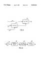
- FIGS. 1a-bare diagrammatic illustrations of the manner in which the present invention may be connected to an electronic device for cancelling distortion caused by non-linearities in the device;
- FIG. 2is a diagrammatic illustration of a distortion cancellation circuit that includes an odd/even-order distortion generator
- FIG. 3is a diagrammatic illustration of an embodiment of the odd/even-order distortion generator
- FIG. 4is a diagrammatic illustration of another embodiment of the odd/even-order distortion generator
- FIG. 5is a diagrammatic illustration of a suitable three-way power combiner
- FIG. 6is a diagrammatic illustration of a suitable equalizer.
- an odd/even distortion cancellation circuit 10may be connected in series with any suitable nonlinear electronic device 12, such as a RF/microwave amplifier, directly modulated laser, light emitting diode, or optical modulator. As illustrated in FIG. 1a, odd/even distortion cancellation circuit 10 may be connected to receive the output of nonlinear device 12 or, equivalently, odd/even distortion cancellation circuit 10 may be connected to provide an input to device 12, as illustrated in FIG. 1b.
- any suitable nonlinear electronic device 12such as a RF/microwave amplifier, directly modulated laser, light emitting diode, or optical modulator.
- odd/even distortion cancellation circuit 10may be connected to receive the output of nonlinear device 12 or, equivalently, odd/even distortion cancellation circuit 10 may be connected to provide an input to device 12, as illustrated in FIG. 1b.
- odd/even distortion cancellation circuit 10comprises a distortion generator 14, which is described in further detail below, a splitter 16, a delay line 18, a three-way combiner 20, and two equalizers 22 and 24.
- Splitter 16may be either an even-split power splitter/combiner or a directional coupler.
- Splitter 16receives an input signal 26 and splits it into a split fundamental signal 28 (V f ) and a split input signal 30 (V i ) having the same phase.
- the relative amplitudes of signals 28 and 30will differ depending on several factors, including the magnitude of input signal 26, the characteristics of device 12, and the characteristics of distortion generator 14.
- Distortion generator 14receives signal 30 and in response produces a first distortion signal 32 (V DIFF ) and a second distortion signal 34 (V SUM ).
- first distortion signal 32consists of the fundamental component and odd-order distortion components of signal 26
- second distortion signal 34consists only of even-order distortion components of signal 26.
- Equalizers 22 and 24provide compensation for differences in frequency-dependent nonlinearity characteristics between device 12 and distortion generator 14. Equalizers 22 and 24 produce a first equalized distortion signal 36 and a second equalized distortion signal 38, respectively. An operator may adjust the phase and/or amplitude of signals 32 and 34 across a predetermined frequency band of interest. Delay line 18 delays signal 28 to produce a delayed signal 40. Three-way combiner 20 receives delayed signal 40 and equalized distortion signals 36 and 38 and combines them in a manner described in further detail below.
- one embodiment of odd/even distortion generator 14may comprise two 180 degree hybrid splitter/combiners 42 and 44 and two non-linear amplifiers 46 and 48.
- Hybrid 42receives split input signal 30 (V i ) and splits it into a first split signal 50 (V 1 ) and a second split signal 52 (V 3 ). Signals 50 and 52 have the same amplitude but differ in phase by 180 degrees.
- Amplifier 46receives split signal 50, and amplifier 48 receives split signal 52.
- Amplifier 46produces a first amplified signal 54 (V 2 ), and amplifier 48 produces a second amplified signal 56 (V 4 ).
- Signals 54 and 56consist of the amplified fundamental signals and both even and odd-order distortion components, which are caused by the nonlinearities inherent in amplifiers 46 and 48.
- Hybrid 44receives signals 54 and 56 and produces first distortion signal 32 (V DIFF ) and second distortion signal 34 (V SUM ).
- first distortion signal 32(V DIFF ) consists of the fundamental and odd-order distortion components of input signal 30, and second distortion signal 34 (V SUM ) consists only of even-order distortion components of input signal 30.
- another embodiment of odd/even distortion generator 14may comprise a power splitter 58, two 180 degree hybrid splitter/combiners 60 and 62, two non-linear amplifiers 64 and 66, a variable attenuator 68, a time delay 70, and a 180 degree power combiner 72.
- Splitter 58 and combiner 72may be either directional couplers or even-split summer/combiners. This embodiment is particularly useful where distortion cancellation would be enhanced by increasing the level of odd-order distortion components in first distortion signal 32 (V DIFF ). If the level of signal 32 is increased using the distortion generator circuit shown in FIG. 3, the level of the fundamental component of signal 32 will increase along with the level of the odd-order distortion components.
- the distortion generator circuit shown in FIG. 4may be used to increase the level of odd-order distortion components without increasing the level of the fundamental component.
- Splitter 58splits input signal 30 (V i ) into a first input signal 74 (V 5 ) and a second input signal 76 (V 6 ) having the same phase.
- Variable attenuator 68adjusts the level of first split input signal 74, and time delay 70 delays the attenuated signal 78 to produce a delayed signal 80.
- the remainder of the circuitis similar to that described above with respect to FIG. 3.
- Hybrid 60splits second input signal 76 into a first split signal 82 (V 1 ') and a second split signal 84 (V 2 '). Signals 82 and 84 have the same amplitude but differ in phase by 180 degrees.
- Amplifier 64receives split signal 82, and amplifier 66 receives split signal 84.
- Amplifier 64produces a first amplified signal 86 (V 3 '), and amplifier 66 produces a second amplified signal 88 (V 4 ').
- Signals 86 and 88consist of the amplified fundamental signals and both even and odd-order distortion components, which are caused by the nonlinearities inherent in amplifiers 64 and 66.
- Hybrid 62receives signals 86 and 88 and produces a first distortion signal 90 (V DIFF ') and second distortion signal 34 (V SUM ).
- Combiner 72subtracts signal 80 from signal 90 and produces first distortion signal 32 (V DIFF ).
- three-way combiner 20must either add or subtract equalized first and second distortion signals 36 and 38 at a phasing that causes suppression of both the odd and even distortions.
- Combiner 20may be formed as shown in FIG. 5.
- a first directional coupler 92combines first and second distortion signals 36 and 38.
- a second directional coupler 94combines signal 40 with the output of coupler 92.
- each couplercombines its input signals either in our out of phase, as known in the art.
- a time delay(not shown) may be used in series with the input to coupler 94 carrying signal 40 in order to equalize delays.
- a nonlinear device 12has a series expansion:
- a jis the j th -order gain coefficient for the device.
- the gain coefficientsmay be negative or positive depending on the inherent nonlinearity of device 12. When a coefficient is negative it has a compressive effect upon V o , and when it is positive it has an expansive effect. For example, when A 1 , A 3 , A 5 , etc. are all negative, the device has compressive odd-order distortions and, when A 2 , A 4 , A 6 , etc. are all positive, the device has expansive even-order distortions.
- Some non-linear devices 12are known to produce compressive distortions and other devices 12 are known to produce expansive distortions.
- a Mach-Zehnder interferometerwhich is commonly used for modulating an optical beam, is known to always produce compressive third-order distortions.
- some devicescan only be determined to be compressive or expansive using empirical methods.
- a semiconductor lasermay have either compressive or expansive distortion characteristics for both odd and even-order distortions.
- signals 36 and 38should be subtracted from delayed signal 40. To cancel compressive distortions, these signals should be added to delayed signal 40. This phase relation must be correct in order for equalized distortion signals 36 and 38 to be exactly opposite in phase with the signals generated by device 12. For example, to cancel third-order distortion produced in a Mach-Zehnder interferometer, A 3 in first distortion signal 32 (V DIFF ) must be added to delayed signal 40.
- any initial phasingmay be selected for the inputs of combiner 20. While observing the input and output signals of the combinations shown in FIG. 1a or 1b, the amplitudes of signals 36 and 38 are adjusted using equalizers 22 and 24 to determine if the output signal is distorted with respect to the input signal over the frequency range of interest. As shown in FIG. 6, each of equalizers 22 and 24 may comprise an amplifier 96, a tunable delay 98, a variable attenuator 100, and a passive filter 102. If adjusting attenuator 100 in either of equalizers 22 or 24 reduces distortion, the phasing of combiner 20 is correct.
- adjusting attenuator 100increases distortion, a different phasing should be selected and the process of adjusting equalizers 22 and 24 repeated.
- the relative phasing of signals 32 and 34may be adjusted using tunable delay 98 in equalizers 22 and 24 in a manner that further reduces distortion.
- Filter 102may be used to add any amplitude equalization necessary to match the amplitude of the generated distortion to that of device 12.
- FIGS. 3 and 4may be used in any suitable distortion cancellation circuit, of which circuit 10 is only illustrative. Obviously, other embodiments and modifications of the present invention will occur readily to those of ordinary skill in the art in view of these teachings. Therefore, this invention is to be limited only by the following claims, which include all such other embodiments and modifications when viewed in conjunction with the above specification and accompanying drawings.
Landscapes
- Physics & Mathematics (AREA)
- Nonlinear Science (AREA)
- Engineering & Computer Science (AREA)
- Power Engineering (AREA)
- Amplifiers (AREA)
Abstract
Description
V.sub.O =A.sub.1 V.sub.i +A.sub.2 V.sup.2.sub.i +A.sub.3 V.sup.3 .sub.i +A.sub.4 V.sup.4.sub.1 +. . .
Claims (6)
Priority Applications (1)
| Application Number | Priority Date | Filing Date | Title |
|---|---|---|---|
| US08/239,466US5428314A (en) | 1994-05-09 | 1994-05-09 | Odd/even order distortion generator and distortion cancellation circuit |
Applications Claiming Priority (1)
| Application Number | Priority Date | Filing Date | Title |
|---|---|---|---|
| US08/239,466US5428314A (en) | 1994-05-09 | 1994-05-09 | Odd/even order distortion generator and distortion cancellation circuit |
Publications (1)
| Publication Number | Publication Date |
|---|---|
| US5428314Atrue US5428314A (en) | 1995-06-27 |
Family
ID=22902254
Family Applications (1)
| Application Number | Title | Priority Date | Filing Date |
|---|---|---|---|
| US08/239,466Expired - Fee RelatedUS5428314A (en) | 1994-05-09 | 1994-05-09 | Odd/even order distortion generator and distortion cancellation circuit |
Country Status (1)
| Country | Link |
|---|---|
| US (1) | US5428314A (en) |
Cited By (11)
| Publication number | Priority date | Publication date | Assignee | Title |
|---|---|---|---|---|
| GB2304246A (en)* | 1995-08-04 | 1997-03-12 | Daimler Benz Aerospace Ag | Arrangement for linearizing the amplitude and phase of TWT or semiconductor amplifiers by summing non-linear components |
| US5834969A (en)* | 1995-07-24 | 1998-11-10 | Mitsubishi Denki Kabushiki Kaisha | Circuit for processing signals from a magneto-resistive head |
| WO1998051007A1 (en)* | 1997-05-02 | 1998-11-12 | Motorola Inc. | Method and apparatus for efficient signal power amplification |
| US5852521A (en)* | 1995-11-28 | 1998-12-22 | Mitsubishi Denki Kabushiki Kaisha | Amplifier circuit suppressing disturbance signal produced by magnetoresistive head |
| WO2000070751A1 (en)* | 1999-05-14 | 2000-11-23 | Harris Corporation | Broadcast transmission system with correction for distortion |
| US6392464B1 (en)* | 1999-09-14 | 2002-05-21 | Lockheed Martin Corporation | Wide bandwidth circuits for high linearity optical modulators |
| US6700442B2 (en)* | 2001-11-20 | 2004-03-02 | Thomas Quang Ha | N way phase cancellation power amplifier |
| US20070098417A1 (en)* | 2005-10-27 | 2007-05-03 | Eva Peral | Distortion cancellation circuitry for optical receivers |
| WO2007102246A1 (en)* | 2006-03-07 | 2007-09-13 | R & K Company Ltd. | Amplifier circuit |
| US20070297803A1 (en)* | 2006-06-21 | 2007-12-27 | Eva Peral | In-line distortion cancellation circuits for linearization of electronic and optical signals with phase and frequency adjustment |
| WO2010028635A1 (en)* | 2008-09-10 | 2010-03-18 | Tesat-Spacecom Gmbh & Co. Kg | Predistortion linearizer with bridge topology having an equalizer stage for each bridge arm |
Citations (7)
| Publication number | Priority date | Publication date | Assignee | Title |
|---|---|---|---|---|
| JPS6019305A (en)* | 1983-07-13 | 1985-01-31 | Nec Corp | Linearizer |
| US4870371A (en)* | 1986-05-02 | 1989-09-26 | Rohde & Schwarz Gmbh & Co. Kg | Network for cascade compensation of the non-linearity of an amplifier |
| US4992754A (en)* | 1989-09-07 | 1991-02-12 | Ortel Corporation | Predistorter for linearization of electronic and optical signals |
| US5077619A (en)* | 1989-10-25 | 1991-12-31 | Tacan Corporation | High linearity optical transmitter |
| US5132639A (en)* | 1989-09-07 | 1992-07-21 | Ortel Corporation | Predistorter for linearization of electronic and optical signals |
| US5161044A (en)* | 1989-07-11 | 1992-11-03 | Harmonic Lightwaves, Inc. | Optical transmitters linearized by means of parametric feedback |
| US5227736A (en)* | 1992-05-18 | 1993-07-13 | Tacan Corporation | Second-order predistorter |
- 1994
- 1994-05-09USUS08/239,466patent/US5428314A/ennot_activeExpired - Fee Related
Patent Citations (8)
| Publication number | Priority date | Publication date | Assignee | Title |
|---|---|---|---|---|
| JPS6019305A (en)* | 1983-07-13 | 1985-01-31 | Nec Corp | Linearizer |
| US4870371A (en)* | 1986-05-02 | 1989-09-26 | Rohde & Schwarz Gmbh & Co. Kg | Network for cascade compensation of the non-linearity of an amplifier |
| US5161044A (en)* | 1989-07-11 | 1992-11-03 | Harmonic Lightwaves, Inc. | Optical transmitters linearized by means of parametric feedback |
| US4992754A (en)* | 1989-09-07 | 1991-02-12 | Ortel Corporation | Predistorter for linearization of electronic and optical signals |
| US5132639A (en)* | 1989-09-07 | 1992-07-21 | Ortel Corporation | Predistorter for linearization of electronic and optical signals |
| US4992754B1 (en)* | 1989-09-07 | 1997-10-28 | Ortel Corp | Predistorter for linearization of electronic and optical signals |
| US5077619A (en)* | 1989-10-25 | 1991-12-31 | Tacan Corporation | High linearity optical transmitter |
| US5227736A (en)* | 1992-05-18 | 1993-07-13 | Tacan Corporation | Second-order predistorter |
Non-Patent Citations (2)
| Title |
|---|
| Childs & O/Byrne, "Multichannel AM Video Transmission Using a High-Power Nd:YAG Laser and Linearized External Modulator," IEEE Journal on Selected Areas in Communications, vol. 8, No. 7, Sep. 1990. |
| Childs & O/Byrne, Multichannel AM Video Transmission Using a High Power Nd:YAG Laser and Linearized External Modulator, IEEE Journal on Selected Areas in Communications, vol. 8, No. 7, Sep. 1990.* |
Cited By (21)
| Publication number | Priority date | Publication date | Assignee | Title |
|---|---|---|---|---|
| US5834969A (en)* | 1995-07-24 | 1998-11-10 | Mitsubishi Denki Kabushiki Kaisha | Circuit for processing signals from a magneto-resistive head |
| GB2304246B (en)* | 1995-08-04 | 1999-12-29 | Daimler Benz Aerospace Ag | Linearisation of amplification and phase characteristics of travelling wave tubes and semiconductor amplifiers |
| GB2304246A (en)* | 1995-08-04 | 1997-03-12 | Daimler Benz Aerospace Ag | Arrangement for linearizing the amplitude and phase of TWT or semiconductor amplifiers by summing non-linear components |
| JP3206722B2 (en) | 1995-08-04 | 2001-09-10 | ダイムラークライスラー・アエロスペース・アクチエンゲゼルシヤフト | Method and apparatus for linearizing the amplification and phase response of traveling wave tubes and semiconductor amplifiers at different output levels |
| US5852521A (en)* | 1995-11-28 | 1998-12-22 | Mitsubishi Denki Kabushiki Kaisha | Amplifier circuit suppressing disturbance signal produced by magnetoresistive head |
| KR100507592B1 (en)* | 1997-05-02 | 2005-08-10 | 모토로라 인코포레이티드 | Method and apparatus for efficient signal power amplification |
| US5892395A (en)* | 1997-05-02 | 1999-04-06 | Motorola, Inc. | Method and apparatus for efficient signal power amplification |
| WO1998051007A1 (en)* | 1997-05-02 | 1998-11-12 | Motorola Inc. | Method and apparatus for efficient signal power amplification |
| WO2000070751A1 (en)* | 1999-05-14 | 2000-11-23 | Harris Corporation | Broadcast transmission system with correction for distortion |
| US6392464B1 (en)* | 1999-09-14 | 2002-05-21 | Lockheed Martin Corporation | Wide bandwidth circuits for high linearity optical modulators |
| US6700442B2 (en)* | 2001-11-20 | 2004-03-02 | Thomas Quang Ha | N way phase cancellation power amplifier |
| US7596326B2 (en) | 2005-10-27 | 2009-09-29 | Emcore Corporation | Distortion cancellation circuitry for optical receivers |
| US20070098417A1 (en)* | 2005-10-27 | 2007-05-03 | Eva Peral | Distortion cancellation circuitry for optical receivers |
| WO2007102246A1 (en)* | 2006-03-07 | 2007-09-13 | R & K Company Ltd. | Amplifier circuit |
| US20090096522A1 (en)* | 2006-03-07 | 2009-04-16 | Etsuo Tsuchiya | Amplifier circuit |
| US20070297803A1 (en)* | 2006-06-21 | 2007-12-27 | Eva Peral | In-line distortion cancellation circuits for linearization of electronic and optical signals with phase and frequency adjustment |
| US7634198B2 (en) | 2006-06-21 | 2009-12-15 | Emcore Corporation | In-line distortion cancellation circuits for linearization of electronic and optical signals with phase and frequency adjustment |
| WO2010028635A1 (en)* | 2008-09-10 | 2010-03-18 | Tesat-Spacecom Gmbh & Co. Kg | Predistortion linearizer with bridge topology having an equalizer stage for each bridge arm |
| US20110169566A1 (en)* | 2008-09-10 | 2011-07-14 | Abdel-Messiah Khilia | Predistorition linearizer with bridge topology having an equalizer stage for each bridge arm |
| US8493143B2 (en) | 2008-09-10 | 2013-07-23 | Tesat-Spacecom Gmbh & Co. Kg | Predistorition linearizer with bridge topology having an equalizer stage for each bridge arm |
| CN102160281B (en)* | 2008-09-10 | 2013-11-13 | 提赛特空间通信有限公司 | Predistortion linearizer with bridge topology having an equalizer stage for each bridge arm |
Similar Documents
| Publication | Publication Date | Title |
|---|---|---|
| US5963352A (en) | Linearization enhanced operation of single-stage and dual-stage electro-optic modulators | |
| US4992754A (en) | Predistorter for linearization of electronic and optical signals | |
| US5252930A (en) | Predistorter for linearization of electronic and optical signals | |
| US5210633A (en) | Apparatus and method for linearizing the operation of an external optical modulator | |
| EP0498456B1 (en) | Predistorter and method for linearization of electronic and optical signals | |
| US5798854A (en) | In-line predistorter for linearization of electronic and optical signals | |
| US6061161A (en) | Distortion-compensation circuit for wideband optical-fiber communication systems | |
| US5963090A (en) | Automatic predistortion adjusting circuit having stable non-linear characteristics regardless of input signal frequency | |
| US5227736A (en) | Second-order predistorter | |
| HK1008408B (en) | Apparatus and method for linearizing the operation of an external optical modulator | |
| US5117197A (en) | High-power feed-forward microwave amplifier apparatus with out-of-band intermodulation product suppression | |
| US5428314A (en) | Odd/even order distortion generator and distortion cancellation circuit | |
| US5258722A (en) | Amplifier circuit with distortion cancellation | |
| US5363056A (en) | Circuit for linearization of amplified electronic signals | |
| AU708748B2 (en) | In-line predistorter for linearization of electronic and optical signals | |
| US6285252B1 (en) | Apparatus and method for broadband feedforward predistortion | |
| US4168511A (en) | Common amplification system for video and audio frequency signals | |
| US4016497A (en) | Feedbackward distortion compensating circuit | |
| US3725806A (en) | Distortion reduction in a repeatered transmission system | |
| US3993961A (en) | Overcompensated feedforward method and apparatus using overdistorted main amplifiers | |
| JP3050254B2 (en) | Low distortion amplifier circuit | |
| IE903084A1 (en) | Apparatus and method for reducing distortion in an analog¹optical transmission system | |
| JPH0794954A (en) | Power amplifier device | |
| JPH0530324B2 (en) | ||
| JPS6017936Y2 (en) | nonlinear circuit |
Legal Events
| Date | Code | Title | Description |
|---|---|---|---|
| AS | Assignment | Owner name:TACAN CORPORATION, CALIFORNIA Free format text:ASSIGNMENT OF ASSIGNORS INTEREST;ASSIGNORS:SWAFFORD, WILLIAM;VAN CLEAVE, TODD;REEL/FRAME:006995/0303 Effective date:19940420 | |
| FEPP | Fee payment procedure | Free format text:PETITION RELATED TO MAINTENANCE FEES FILED (ORIGINAL EVENT CODE: PMFP); ENTITY STATUS OF PATENT OWNER: SMALL ENTITY | |
| FEPP | Fee payment procedure | Free format text:PETITION RELATED TO MAINTENANCE FEES GRANTED (ORIGINAL EVENT CODE: PMFG); ENTITY STATUS OF PATENT OWNER: SMALL ENTITY | |
| AS | Assignment | Owner name:UNION BANK OF CALIFORNIA, N.A., CALIFORNIA Free format text:SECURITY AGREEMENT;ASSIGNOR:TACAN CORPORATION;REEL/FRAME:009703/0068 Effective date:19981230 | |
| REMI | Maintenance fee reminder mailed | ||
| AS | Assignment | Owner name:CIT GROUP/CREDIT FINANCE, INC., THE, CALIFORNIA Free format text:SECURITY AGREEMENT;ASSIGNOR:TACAN CORPORATION;REEL/FRAME:009958/0196 Effective date:19990423 | |
| FP | Lapsed due to failure to pay maintenance fee | Effective date:19990627 | |
| FPAY | Fee payment | Year of fee payment:4 | |
| SULP | Surcharge for late payment | ||
| PRDP | Patent reinstated due to the acceptance of a late maintenance fee | Effective date:19991029 | |
| AS | Assignment | Owner name:TACAN CORPORATION, CALIFORNIA Free format text:SECURITY INTEREST;ASSIGNOR:UNION BANK OF CALIFORNIA N.A.;REEL/FRAME:010892/0422 Effective date:19990708 | |
| AS | Assignment | Owner name:TACAN CORPORATION, CALIFORNIA Free format text:RELEASE;ASSIGNOR:CIT GROUP/BUSINESS CREDIT, INC.;REEL/FRAME:011159/0126 Effective date:20000626 | |
| LAPS | Lapse for failure to pay maintenance fees | ||
| STCH | Information on status: patent discontinuation | Free format text:PATENT EXPIRED DUE TO NONPAYMENT OF MAINTENANCE FEES UNDER 37 CFR 1.362 | |
| FP | Lapsed due to failure to pay maintenance fee | Effective date:20030627 |