US5426075A - Method of manufacturing ferroelectric bismuth layered oxides - Google Patents
Method of manufacturing ferroelectric bismuth layered oxidesDownload PDFInfo
- Publication number
- US5426075A US5426075AUS08/259,870US25987094AUS5426075AUS 5426075 AUS5426075 AUS 5426075AUS 25987094 AUS25987094 AUS 25987094AUS 5426075 AUS5426075 AUS 5426075A
- Authority
- US
- United States
- Prior art keywords
- layer
- film
- depositing
- target
- ferroelectric
- Prior art date
- Legal status (The legal status is an assumption and is not a legal conclusion. Google has not performed a legal analysis and makes no representation as to the accuracy of the status listed.)
- Expired - Fee Related
Links
Images


Classifications
- H—ELECTRICITY
- H10—SEMICONDUCTOR DEVICES; ELECTRIC SOLID-STATE DEVICES NOT OTHERWISE PROVIDED FOR
- H10D—INORGANIC ELECTRIC SEMICONDUCTOR DEVICES
- H10D1/00—Resistors, capacitors or inductors
- H10D1/60—Capacitors
- H10D1/68—Capacitors having no potential barriers
- H10D1/682—Capacitors having no potential barriers having dielectrics comprising perovskite structures
- H10D1/684—Capacitors having no potential barriers having dielectrics comprising perovskite structures the dielectrics comprising multiple layers, e.g. comprising buffer layers, seed layers or gradient layers
- C—CHEMISTRY; METALLURGY
- C23—COATING METALLIC MATERIAL; COATING MATERIAL WITH METALLIC MATERIAL; CHEMICAL SURFACE TREATMENT; DIFFUSION TREATMENT OF METALLIC MATERIAL; COATING BY VACUUM EVAPORATION, BY SPUTTERING, BY ION IMPLANTATION OR BY CHEMICAL VAPOUR DEPOSITION, IN GENERAL; INHIBITING CORROSION OF METALLIC MATERIAL OR INCRUSTATION IN GENERAL
- C23C—COATING METALLIC MATERIAL; COATING MATERIAL WITH METALLIC MATERIAL; SURFACE TREATMENT OF METALLIC MATERIAL BY DIFFUSION INTO THE SURFACE, BY CHEMICAL CONVERSION OR SUBSTITUTION; COATING BY VACUUM EVAPORATION, BY SPUTTERING, BY ION IMPLANTATION OR BY CHEMICAL VAPOUR DEPOSITION, IN GENERAL
- C23C14/00—Coating by vacuum evaporation, by sputtering or by ion implantation of the coating forming material
- C23C14/06—Coating by vacuum evaporation, by sputtering or by ion implantation of the coating forming material characterised by the coating material
- C23C14/08—Oxides
- C23C14/086—Oxides of zinc, germanium, cadmium, indium, tin, thallium or bismuth
Definitions
- This inventionrelates generally to a method of forming a ferroelectric film for use as the dielectric of a capacitor memory element for a nonvolatile memory. More particularly, the present invention relates to a manufacturing method using bismuth layered oxide compounds having the desirable electrical characteristic that is compatible with conventional integrated circuit processing.
- PZTlead zirconate titanate
- bismuth layered compoundsare also ferroelectric.
- the structure of bismuth layered compoundsconsists of layers of perovskite, infinite in two dimensions, separated from each other by a bismuth oxide layer.
- the perovskite layercan be one, two, three or more perovskite unit cells thick. Each of these thicknesses results in a separate structure type, but has the perovskite layer-bismuth oxide layer alternation, giving rise to the term bismuth "layered” compounds.
- ferroelectric bismuth layered compoundsinclude bismuth titanate (Bi 4 Ti 3 O 12 ) and strontium bismuth tantalate (SrBi 2 Ta 2 O 9 ), which is also known as "SBT", as well as many others.
- the reversible polarization of a ferroelectric material filmmust be in a direction perpendicular to the plane of electrodes that transfer the applied electric field to the film so that an appreciable amount of charge can be detected.
- a stable polarizationresults from the alignment of internal dipoles with the perovskite crystal units in the ferroelectric material.
- Application of the .electric field across a ferroelectric materialcauses the alignment of the dipoles in one direction. Reversal of the polarity of the applied field also reverses, or switches, the alignment of the internal dipoles.
- Hysteresis curve 10Atherefore demonstrates the electrical behavior of a ferroelectric material such as PZT wherein the x-axis represents the applied electric field and the y-axis represents the resultant polarization or charge.
- Two stable states 12A and 14Aare shown in FIG. 1A, which represent opposite alignments of the internal dipoles after the applied electric field has been removed.
- the amount of charge released in moving between stable states 12A and 14Ais known as the "switched charge.”
- the rate of alignment of the dipolesis related to the overdrive voltage, i.e. the amount by which the applied voltage exceeds the coercive voltage.
- the position of the dipoles and the associated electric charge in response to an applied electric fieldcan be detected with appropriate sensing circuitry.
- Ferroelectric materialstherefore, can be used as the dielectric material in a ferroelectric capacitor that in turn is used as the memory element in a nonvolatile memory cell.
- Hysteresis curve 10B in FIG. 1Bdemonstrates the electrical behavior of a ferroelectric material such as SBT wherein the x-axis represents the applied electric field and the y-axis represents the resultant polarization or charge.
- the coercive voltageis about one volt and the saturation voltage is about 2.5 volts.
- hysteresis curve 10Bhas a roughly square shape, which is indicative of a well defined coercive voltage, i.e. most of the dipoles have been switched at the coercive voltage level of applied electric field.
- two stable states 12B and 14Bare shown in FIG. 1B, which represent opposite alignments of the; internal dipoles after the applied electric field has been removed.
- ferroelectric bismuth compoundsare well suited to operation in a memory because of their electric characteristics, they are difficult to manufacture as a capacitor dielectric material in a typical semiconductor processing flow.
- a classical method of depositing bismuth titanate, or other bismuth ferroelectric materialsis to sputter the material from a single target at elevated temperatures onto crystalline planes of a substrate oxide.
- the substrate oxideis chosen so that the lattice dimensions are matched to the lattice dimensions of the ferroelectric bismuth compound, which results in a crystalline film that is ferroelectric.
- the classical sputter deposition methodsuffers from several shortcomings.
- the common substrates used to lattice match with the ferroelectric filmsuch as aluminum oxide, lanthanum aluminum oxide, magnesium aluminum oxide or magnesium oxide, are not conductive.
- conductive electrodesare required in order to apply an electric field across the ferroelectric film.
- the ferroelectric filmmust be physically peeled from the substrate and electroded. After separation from the substrate, the films are very fragile and difficult to handle. Therefore the process of using such films is very difficult and unsuitable for fabrication of conventional nonvolatile memories. It is conceivable that there might exist a conductive oxide that could also provide lattice matching, but the known conductive oxides suffer from poor conductivity, thermal instabilities, and complex fabrication methods.
- spin-on deposition methodssuch as sol gel or metal organic deposition, may yield switching bismuth layered oxide films on conductive electrodes, but these methods also suffer from several shortcomings.
- the orientation of grains and grain size of the deposited filmmight not be suitable or controllable when used on bottom electrodes suitable for conventional integrated circuit processing, resulting in a low grade ferroelectric material that yields little switched charge.
- spin-on deposition methodssuffer from practical incompatibilities with the processing techniques used in the fabrication of conventional semiconductor integrated circuit non-volatile memories.
- Spin-on depositionplanarizes the surface topography on top of an integrated circuit by becoming thicker in the troughs and thinner at elevated surface features.
- This non-uniform film thickness depositioncauses problems during subsequent patterning steps, resulting in regions of under etching and regions of over etching.
- Another problem with spin-on deposition techniquesis that the availability of suitable precursor solutions is not as commercially developed as the availability of sputter targets for the deposition process referred to above. The purity requirement of near zero mobile ion content is readily achieved with commercially available metal oxide powders used for sputtering targets, but remains a challenge for spin-on sources.
- the spin-on processis susceptible to a host of additional problems such as precipitation of detrimental particles in the solution or during application, streaking, poor adhesion, and film cracking due to volumetric changes during solvent evolution bakes.
- Another alternative prior art deposition methodis the technique of "co-deposition" in which two or more targets are used, primarily to control the composition of a deposited film.
- the deposition from multiple targetsis either done simultaneously or separately, but in the latter case with extremely thin layers.
- the layer thicknessmay be only a few Angstroms thick, in which case there is an effective mixing of layers to form a homogeneous film composition.
- This techniqueas now commonly practiced, is not useful for forming bismuth layered ferroelectric films. While the resultant film composition is made of the desired constituent elements, and in the proportions required, the film is not ferroelectric.
- CMOScomplementary metal oxide semiconductor transistor
- ferroelectric filmsand in particular, bismuth layered ferroelectric films with a large amount of reversible polarization in a direction perpendicular to the plane of electrodes attached to the film.
- Another object of the inventionis to provide a deposition method that is compatible with conventional integrated circuit processing techniques.
- An advantage of the inventionis that it can be applied to a wide variety of ferroelectric compounds and in particular to bismuth layered ferroelectric compounds that have desirable electrical properties.
- the preferred deposition methodis independent of the specific characteristics of the substrate or bottom electrode.
- the present inventionis a semiconductor manufacturing method for forming a ferroelectric film, and in particular, a ferroelectric film of the bismuth layered structure type, that has a significant component of reversible polarization perpendicular to the plane of the electrodes attached to that film.
- the manufacturing methodis conducted at low temperatures on commercially suitable electrodes and is compatible with conventional CMOS fabrication techniques.
- the present inventionincludes a sputtering process that uses multiple sputtering targets and sequential deposition to form a precursor film in thin but distinct and unmixed layers, which is subsequently annealed to convert the the distinct layers into a composite ferroelectric film.
- the capacitors made with such a filmare ferroelectric in that a significant switched charge (at least five uC/cm 2 ) can be detected with a conventional sense amplifier in response to an applied electric field.
- a ferroelectric SBT filmis formed using two sputtering targets.
- a first sputtering targetis comprised primarily of bismuth oxide (Bi 2 O 3 ) and a second sputtering target is comprised primarily of SBT (SrBi 2 Ta 2 O 9 ).
- An initial layer of bismuth oxideis formed on a bottom electrode of a ferroelectric capacitor stack. The initial layer of bismuth oxide is directly followed by a sputtered layer of bismuth deficient SBT.
- a second layer of bismuth oxideis then applied and the layers are sequentially alternated in a "layer cake" fashion containing a plurality of layers until a desired thickness of the film is attained.
- a crystallization annealis performed to make the film ferroelectric. It is inferred that the "layer cake" structure is necessary, once annealed, to properly orient the grains of the polycrystalline film. Once the ferroelectric film is in place, a top electrode is formed and all remaining semiconductor processing steps are completed.
- FIG. 1Ais a plot of a hysteresis curve associated with a ferroelectric material such as PZT having a poorly defined coercive voltage
- FIG. 1Bis a plot of a hysteresis curve associated with a bismuth layered ferroelectric material such as SBT having a well defined coercive voltage;
- FIG. 2is an illustration of sequential sputter deposition from two targets of different compositions
- FIG. 3is a diagram of a multiple-target sputtering system according to the present invention.
- FIG. 4is a diagram of the substrate transport mechanism of the sputter deposition system shown in FIG. 3 showing the planetary orbit and the wafer spin;
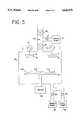
- FIG. 5is a diagram showing the locations of the orbit stop positions of the substrate transport mechanism shown in FIG. 4;
- FIG. 6is a flow diagram of a scanning program that controls the sputtering system shown in FIGS. 3-5;
- FIGS. 7A through 7Dare cross sectional diagrams of the sputtering technique of the present invention showing the accumulation of sequentially deposited layers of different compositions;
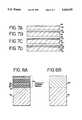
- FIG. 8Ais a cross sectional diagram showing a substrate with a completely fabricated ferroelectric film having discrete layers according to the method of the present invention, but before the annealling step, so that the individual film layers are visible;
- FIG. 8Bis a cross sectional diagram showing the substrate and ferroelectric film of FIG. 8A after the annealling step, in which there is a dissolution of the individual film layers into a homogeneous fine grain polycrystalline film;
- FIG. 9is a cross sectional diagram of the first cycle of individual film layers associated with a four target alternative method of the present invention.
- FIGS. 10A through 10Care cross sectional diagrams showing the sequential evolution of a ferroelectric capacitor structure during a fabrication process, wherein the ferroelectric dielectric material is fabricated according to the method of the present invention.
- FIG. 11is a cross sectional diagram of a ferroelectric capacitor structure according to the present invention fabricated in an integrated circuit, wherein the top and bottom electrodes of the ferroelectric capacitor are contacted by a metallization layer.
- a sputtering deposition methodfor creating ferroelectric films from bismuth layered oxide or other such compounds that is compatible with conventional semiconductor fabrication techniques.
- a ferroelectric filmwhich cart be formed of bismuth layered materials such as SBT or other ferroelectric materials, is formed using multiple targets 16 and 18 in a sputter deposition process, which is followed by a crystallization anneal.
- the source material from which a thin film is deposited in a sputtering systemis known as the target.
- the target 16, 18is typically bonded to a copper disc, known as the backing plate (not shown in FIG. 2), by either silver epoxy or indium and tin solder.
- the backing plateis mechanically attached to a cathode assembly that houses a cathode, such as cathode 15 and 17 for receiving electrical power, magnets and cooling water (the latter two elements are not shown in FIG. 2).
- the cathode 15, 17is electrically connected to a power supply such as power supplies V 1 and V 2 .
- a radio frequency (“RF") power supplywith an impedance matching network is used to electrically bias the target.
- RFradio frequency
- the negative bias developed on the targetcauses positively charged ions in a plasma contained within the sputtering system to bombard the target 16, 18 with sufficient energy to knock off, or sputter, atoms from the target.
- a portion of the sputtered atomsstick to a substrate 20 such as a silicon integrated circuit wafer and gradually form a deposited film. Consequently, the composition of the deposited film is related to the composition of the target.
- the film and target compositionmay differ considerably in detail since tile sputtered atoms must actually reach and stick to the substrate 20.
- More than one targetis used in the sputtering process of the present invention for the deposition of discrete individual material layers.
- Each target 16 and 18is electrically biased by attached cathodes 15 and 17, respectively, which are in turn energized by respective RF power supplies V 1 and V 2 . Shielding around targets 16 and 18 (not shown in FIG. 2) and the relative spacing between targets 16 and 18 and substrate 20 reduce mixing of the sputtered material in the deposition chamber.
- Substrate 20is movable, and supported beneath and transported between each target 16 and 18 via wafer support 21 to enable the formation of a film with alternating discrete layers of differing composition by sequential deposition from each target 16, 18.
- a target such as target 16 and 18 shown in FIG. 2must be mechanically robust enough to withstand thermal gradients developed by the sputtering process and the associated water cooled cathode. Also, the mobile ion content of the target from contaminating compounds such as lithium, sodium, and potassium is desirably very low due to the semiconductor application.
- An insulating or oxide targetcan be fabricated by conventional ceramic fabrication methods. Commercially available high purity metal oxide powders are weighed according to the desired target composition. After mechanically mixing the individual powders, the combined powder is contained in a graphite die and subjected to high pressure at elevated temperatures in a hot press to consolidate the powder into a single ceramic piece.
- the targetcan be a mixture of reaction products, or material phases, formed during the hot pressing.
- the starting powdersare mixed and fully reacted in a furnace.
- the reacted powderis milled to a fine size and, in order to minimize mobile ion contamination, a binder is not added.
- the powderis consolidated by a cold press to a low density, or green, ceramic piece. The piece is then sintered at high temperatures for long times to increase density and mechanical integrity.
- the preferred compositions of the two targets 16, 18 used in a first method of the present inventionare bismuth oxide, Bi 2 O 3 and SBT, Sr 1 Bi 2 Ta 2 O 9 .
- the size of the bismuth oxide targetis ideally 2.73 inches in diameter by 0.25 inches thick mounted on a three inch diameter copper backing plate.
- the size of the SBT targetis ideally 4.73 inches in diameter by 0.25 inches thick mounted on a five inch diameter copper backing plate.
- the stated purity level of the SBT targetcan be as low as 0.995 due to a typically high content of barium in the strontium and, to a lesser extent, traces of niobium in the tantalum.
- FIG. 3A multiple-target sputtering, system for use in the sputtering method of the present invention is illustrated in FIG. 3.
- the preferred sputtering systemincludes a PVD-300 physical vapor deposition system manufactured by Unifilm Technology, Inc. of Boulder, Colo., although other commercially available sputtering equipment can be adapted and used.
- a deposition chamber 40is equipped with a mechanical roughing pump 43 and a high vacuum cryogenic pump 44. Sequential operation of the roughing pump 43 and cryogenic pump 44 is controlled through valves 48 and 49.
- the sputtering system of FIG. 3preferably includes a load lock chamber 32 that allows load lock operation when introducing substrates or wafers into the deposition chamber 40.
- a waferfor example, is introduced into the load lock chamber 32 by means of a valve 45.
- a valve 47is opened, which allows roughing pump 41 to pull a vacuum in chamber 32.
- valve 46is opened and the wafer is introduced into deposition chamber 40 by mechanical means (not shown in FIG. 3).
- cathodes 15 and 17are shown in FIG. 3, but as many as four can be used.
- the number of cathodes and corresponding targetsis linked to the type of equipment used. The number of cathodes, therefore, may be increased if permitted by the available locations in the equipment used.
- the operation of a four cathode/four target systemis described in further detail below.
- the cathodes 15 and 17 shown in FIG. 3are ideally manufactured by the Kurt J. Lesker Company of Clairton, Pa. and by Vacuum Incorporated of Boulder, Colo. Each cathode 15 and 17 is powered by a separate 13.54 megahertz radio frequency power supply designated. V 1 and V 2 . Ideally, power supplies and matching networks manufactured by the Plasmatherm Company of Kresson, N.J.
- the cathodes 15 and 17, and attached targets 16 and 18,are positioned in a circle above the substrate transport mechanism 30.
- the target to substrate distanceis about 1.75 inches for the 4.73 inch diameter targets, and the target to substrate distance is about 3.5 inches for the 2.73 inch diameter target.
- the substrate transport mechanism 30is rotated by motor 42 and is controlled to provide a uniform deposited film thickness and target selection. This control process is explained in greater detail below with reference to FIGS. 4 and 5.
- Substrate transport mechanism 30also includes a number of wafer supports of which wafer supports 21A, 21B, and 21C are shown. All wafer supports are rotated and controlled together as a group.
- one or more substrates or wafers 20are loaded into the vacuum deposition chamber 40 by means of load lock chamber 32 followed by a pause of a few minutes to return to a base pressure of less than 5E-7 Torr.
- the substrate holders 21A-Care preferably not heated by a substrate heater although the sputter process does raise the substrate temperature somewhat.
- the vacuum pump 44is throttled down and the deposition chamber 40 is back filled with argon. After positioning the substrate 20 away from the direct Spray of either target 16 or 18, power is applied to each target 16 or 18 and a plasma is ignited.
- a time period of about fifteen secondsis used to establish the desired target powers and effectively serves as a presputter period to clean the target surfaces of any background gas accumulation.
- a computer controlled mechanical substrate scanning programis subsequently started that sequentially moves the substrate beneath each target in a well defined fashion to accumulate discrete individual layers of differing composition from each target. The scanning program is described below in further detail, and particularly with respect to the program flow chart of FIG. 6 and accompanying text. Referring again to FIG. 3, after a predetermined time period the target power and argon gas is shut off, and the substrate 20 is removed from the vacuum deposition chamber 40 through the load lock chamber 32.
- the substrate or wafer 20A through 20E at a timeis coated by sputtering from one of the two biased targets 16 or 18.
- the substrate or wafer 20A-Eis always spinning, and the spin rate is rapid enough so that at least one full spin occurs at each orbit stop.
- the orbit drive stopsat eight different locations with four orbit stop locations (each set of four locations is denoted by an "X") symmetrically located near or beneath each target as shown in FIG. 5. It is important to note that the orbit stops as shown in FIG. 5 are not coaxial with the targets 16 and 18, as the non-coaxial locations appear to improve the yield of the sputtering process.
- the non-coaxial locationlowers the energy of the sputtered material onto the surface of the wafer 20, which may have a desirable effect on the final orientation of the crystal grains in the ferroelectric material film.
- the time delay at each orbit stop positionis adjusted to give the desired thickness uniformity across the substrate, since there is more surface area at the periphery of a wafer than at the center of a wafer. (This is primarily due to the fact that the target 16 or 18 is smaller than the wafer. The targets are about three inches in diameter, whereas the wafer 20 is about six inches in diameter. Also, recall that the spacing between the target and the wafer is as much as 3.5 inches.) After completion of the sequence of eight orbit stops, the orbit direction is reversed.
- the sequenceis repeated until the desired number of layers and the desired overall deposited film thickness is obtained.
- This scan method yieldis excellent across wafer uniformity, but suffers from low throughput.
- the low throughputis caused by not positioning the wafer directly beneath the target where deposition rate is greatest and by coating only one substrate at a time.
- the orbit stop positionsare used twice during each cycle of the scanning program. They are used once as the wafer moves closer toward the target and then again as the wafer moves away.
- This "come and go" scanning motioninvolves a direction reversal during each cycle of steps 108 to 114 and 116 to 122 as is explained below with respect to the scanning program flow chart shown in FIG. 6. Reversal of the orbit motion reduces the time required for deposition by eliminating extraneous orbital wafer transport through a complete rotation.
- the orbital and planetary motion described hereinis highly dependent upon the type of deposition machine used, and can therefore be changed as desired to fit the constraints of different deposition machinery or for a different application.
- the scanning program to control the two-target method of the present inventionis further explained with reference to the program flow chart 100 of FIG. 6.
- the flow chart 100begins at step 102 in which the number of discrete layer pairs LP is equal to zero.
- Decision point 104asks whether the number of layer pairs LP is equal to a desired final number of layer pairs K. If the answer is yes, the process is ended at step 106. If the answer if no, wafer 20 is positioned at the first or next orbit stop at step 108. Once at the proper orbit stop, bismuth oxide is deposited by sputtering at step 110.
- Decision point 112asks whether the deposition time T 1 is equal to a desired bismuth oxide deposition time T M .
- step 114asks whether the last orbit stop has been reached. If the answer is yes, the program continues to place wafer 20 at the first orbit stop for the SBT deposition. If the answer is no, the program returns to step 108 to position wafer 20 at the next orbit stop.
- step 116the wafer 20 is placed at the proper orbit stop. SBT is subsequently deposited by sputtering at step 118.
- Decision point 120asks whether the deposition time T 2 is equal to a desired SBT deposition time T N . If the answer is yes, the program continues to the last orbit stop at decision point 122. If the answer is no, the program returns to step 118 to continue the deposition.
- Decision point 122asks whether the last orbit stop has been reached. If the answer is yes, a full layer pair of bismuth oxide/SBT has been deposited and the scanning program returns wafer 20 to the first orbit stop for a new round of bismuth oxide deposition or an end to the program at decision point 104. The current status of the number of layer pairs ("LP") is incremented by one at step 124. If the answer is no, the program returns to step 116 to position wafer 20 at the next orbit stop.
- LPcurrent status of the number of layer pairs
- the sputter gas compositionis argon without added oxygen at a pressure of about 5 mTorr.
- the RF forward power applied to the bismuth target 16is about 90 Watts, and the RF forward power applied to the SBT target 18 is about 200 Watts.
- the target powersare adjusted to control the aggregate "as-deposited" bismuth film composition to lie within 3% of a 42% optimum value as determined by ICP (inductively coupled plasma spectroscopy), i.e. 39% to 45%.
- the tantalum-to-strontium ratio of the aggregate as deposited filmis about 2.2, and is determined by the relative tantalum to strontium content of the SBT target.
- a substrate or bottom electrode 50is shown having a single deposited layer 52 of bismuth oxide following deposition from a bismuth oxide target onto the wafer as described above.
- bismuth oxideis always used as the initial sputtered layer to desirably control grain size and possibly orientation in the final annealed ferroelectric film.
- a layer 54 of bismuth deficient SBThas been deposited on top of the initial bismuth oxide layer 52 following deposition from an SBT target onto the wafer as described above. Layers 52 and 54 together constitute a layer pair, representing one full sputtering cycle. The number of layer pairs in the film is thus equal to the number of repetitive full cycles in the scan program as described with reference to FIG. 6.
- an additional layer pair of a bismuth oxide layer 56 and an SBT layer 58are deposited through the sputtering process. There are, therefore, two layer pairs shown in FIG. 7D. Additional layers are accumulated by multiple sputtering cycles.
- the combined thickness of one bismuth oxide layer and one SBT layercan be determined by measuring the total as-deposited film layer thickness and dividing by the number of cycles in the scan program. The as-deposited film thickness is adjusted to be between about 50 Angstroms and 200 Angstroms.
- a typical film thickness of one complete cycle(a layer pair in using a two-target process) is approximately 75 Angstroms, wherein the bismuth oxide layer is about 15 Angstroms and the SBT layer is about 60 Angstroms.
- Twenty-six layer pairsgive a total film thickness of about 2000 Angstroms.
- the layer thicknessesare determined by controlling the deposition rates and deposition times in the sputtering method under control of the scan program. They may be modified if desired for a particular application.
- the first or bottom layer of the structuremay be either SBT or bismuth oxide
- the preferred initial layeris bismuth oxide because a fine grain structure is produced and the electrical switching characteristics are improved.
- the initial layer of bismuth oxidemay serve to properly orient the grains in the film once it has been annealed.
- the as-deposited "layer cake” film structure shown in FIG. 7Dmust be crystallized in order to realize ferroelectric properties. This is done by furnace-annealing the intermediate product of the multilayer deposition process described above.
- the discrete amorphous layersare transformed into a homogeneous polycrystalline film having a structure composed of crystalline ferroelectric grains as shown in FIGS. 8A and 8B.
- a substrate 50receives a plurality (eleven layer pairs are shown) of alternately deposited layers to comprise a film 60, of which representative bismuth oxide layers 52 and 56, and bismuth deficient SBT layers 54 and 58 are labeled.
- the structure shown in FIG. 8Ais subsequently subjected to a crystallization anneal to establish a ferroelectric film 60'.
- the crystallization of layers in film 60is accomplished by annealing in a conventional hot wall quartz tube furnace in oxygen at an approximate flow of about five liters per minute, at a temperature of about 800° C., and for a time period of about one hour.
- the deposition method described aboveresults in a ferroelectric film comprised of bismuth layered oxide ferroelectric compounds such as SBT.
- the resultant ferroelectric filmprimarily exhibits desirable memory cycling characteristics, low voltage operation, and retention properties.
- the deposition method described abovealso influences to a lesser extent many other desirable electrical properties such as rapid saturation of the switched charge at low voltages, stability of switched charge over time and temperature treatments, and stability of the electrical characteristics during integrated circuit processing.
- two ceramic targetsare fabricated and used in a manner similar to the previous method except that the compositions of the two targets are bismuth oxide, (Bi 2 O 3 ) for the first target and strontium tantalum oxide, (formulated Sr 1 Ta 1 .75 O 5 .38) for the second target.
- the diameter of both targetsis about 2.73 inches.
- Torus cathodeobtained from the Lesker company was used for the bismuth target. This cathode gives a higher deposition rate compared to the cathode used in the previously described method.
- the deposition system and wafer scan program usedare substantially the same as described in the previous embodiment, the major difference being the composition of the second target.
- the method and procedures used for deposition of the thin filmare similar to that previously described, except the target power used in this method 35 Watts for the bismuth oxide target and 100 Watts for the strontium tantalum oxide target.
- the optimum as-deposited aggregate composition of the ⁇ layer cake ⁇ layered structureis slightly richer in bismuth and has a composition of Sr 0 .155 Bi 0 .47 Ta 0 .375.
- the as deposited tantalum to strontium composition ratiois about 2.4, instead of the ideal ratio of two. Since there is no bismuth component in one of the layers, the bismuth layer thickness component of the ⁇ layer cake ⁇ structure is thicker than in the previous embodiment.
- the composition of the strontium tantalum oxide targetcan be modified to change the composition of the as-deposited film.
- a strontium tantalum target, formulated Sr 1 Ta 1 .65 O 5 .38achieves a tantalum to strontium composition ratio closer to the ideal of two. While two alternative two-target compositions are presented, it is appreciated that many slight alterations of the exact composition may result in an as-deposited film that is closer to the ideal SBT ratio of 1-2-2. This is especially true when all of the variations in deposition equipment and systems are taken into account for any individual sputtering system.
- the targetsare: a three inch diameter bismuth oxide target; a three inch diameter strontium tantalate target, formulated as Sr 1 Ta 1 .75 O 5 .38 ; a five inch diameter bismuth oxide target; and a five inch diameter SBT target, formulated as Sr 1 Bi 2 Ta 1 .9 O 8 .75.
- the disparity in size between the targetsare an artifact of the deposition equipment used, and may be changed as required for other deposition equipment.
- the targetsare arranged in the sputter system in the following sequential order: strontium tantalate; five inch bismuth oxide; bismuth strontium tantalate; and three inch bismuth oxide.
- the substrate scan pattern used in this methoddiffers from the previously described methods in that there is no reversal of the orbit direction.
- this patternthere are eight orbit stops adjacent or near each target and all five planets can be utilized simultaneous for film deposition.
- Each waferis coated by all four targets in sequence as it traverses underneath, building up the discrete layers until the total film thickness is achieved. The sequence of material layers is described in further detail below.
- the periodic structure of the as deposited ⁇ layer cake ⁇ filmconsists of four individual layers corresponding to the deposition of material from each target as shown in FIG. 9.
- the RF power appliedis as follows: 35 Watts for the three inch bismuth oxide target; 100 Watts for the strontium tantalate target; 200 Watts for the strontium bismuth tantalate target; and 25 Watts for the five inch bismuth oxide target.
- the as-deposited composition of the filmis Sr 0 .165 Bi 0 .445 Ta 0 .40, giving a tantalum to strontium composition ratio of approximately 2.4.
- the targetscan be powered on at the same time and then the substrate scanning program can be begun. If four substrates occupy the planets, then the first, or bottom, layer of each ⁇ layer cake ⁇ stack will be different and correspond to each different target. Since the first layer controls the grain size that forms during the crystallization anneal, it is not desirable to use this approach, but the targets should be powered on initially in sequence so that all of the wafers receive the same bottom layer. Desirable fine grain films and orientation are obtained when the first layer is from the three inch or five inch bismuth oxide target, and undesirable coarse grain films are obtained when the first layer is either strontium tantalate or strontium bismuth tantalate.
- the switching characteristics of films with a first layer from the three inch bismuth oxide targetare improved over films with a first layer from the five inch bismuth oxide target. Presumably this is due to some small difference in thickness or due to some other film difference arising from the differing target to substrate distances.
- Fine grain materialis desired for uniformity of physical properties over small distances. The fine grain material can be obtained for substrates on all planets by powering on the targets sequentially in time synchronized with the orbit position so that each substrate has the same type of material in the first layer. Each of the four targets is energized in sequence, starting with a first bismuth oxide target. The power-on sequence is finished once all four targets have been turned on. After deposition of all layers to a desired thickness, a crystallization anneal is performed that is identical to that previously described.
- the as-deposited layers for an ideal film .deposited during one cycle of the scanning program adapted for this alternative methodare shown in FIG. 9.
- a substrate 50is shown, which can be the bottom electrode metallization on a silicon wafer or any other substrate.
- a desirable first material layer 72is bismuth oxide, which is about 20 Angstroms thick
- a second material layer 74is SBT, which is about 90 Angstroms thick
- a third material layer 76is again bismuth oxide, which is about 20 Angstroms thick
- a fourth material layeris strontium tantalate, which is about 50 Angstroms thick.
- the as-deposited film thickness for one total cycleis about 180 Angstroms thick.
- the total film thicknessis about 2000 Angstroms thick, corresponding to about eleven cycles of the scanning program or eleven sets of the four material layers.
- FIGS. 10A-CA series of fabrication steps is shown in the cross sectional diagrams of FIGS. 10A-C, in which the sputtering deposition method of the present invention is used to produce a ferroelectric capacitor dielectric layer 88 for a non-volatile memory element in an integrated circuit.
- the capacitor stack 80 shown in FIGS. 10Cis a desirable arrangement of material layers for making a ferroelectric capacitor in a process compatible with conventional integrated circuit CMOS fabrication techniques.
- a bottom electrodeis deposited by sputtering onto an oxide layer 82 of a semiconductor wafer substrate 50.
- the oxide layer 82is preferably about 5000 Angstroms thick.
- a bottom electrode structureis comprised of a titanium adhesion layer 84, which is about 200 Angstroms thick and deposited on the surface of the oxide layer 82.
- a platinum layer 86which is about 1750 Angstroms thick is deposited onto the surface of the titanium adhesion layer 84, and forms the surface of the bottom electrode for subsequent interface to a ferroelectric film layer formed according to the method of the present invention.
- a layered film 88is then established as a dielectric layer over the bottom electrode .as described in any of the previous methods.
- the layered film 88is desirably about 2000 Angstroms thick.
- the layered film 88is converted to a ferroelectric film after crystallizing anneal is performed.
- a top electrode 90is deposited by sputtering onto the layered dielectric film 88 and is preferable comprised of platinum.
- the top electrode layer 90is desirably about 1750 Angstroms thick.
- FIG. 11A more realistic rendering of an integrated circuit ferroelectric capacitor in which the dielectric was formed according to the techniques of the present invention is shown in FIG. 11. Note that the order of layers 82-90 is unchanged, but that the ferroelectric layer is etched back from the bottom electrode, and the top electrode layer is etched back from the ferroelectric dielectric layer 88.
- oxide isolation features 83are included to electrically isolate an integrated circuit metallization consisting of layers 92 and 94.
- Metallization layer portions 92A and 94Aform the metallization for the top electrode of the capacitor, and metallization layer portions 92B and 94B form the metallization for the bottom electrode of the capacitor as shown in FIG. 10.
- the bottommost layers 92A and 92Bare formed of titanium nitride (TiN), about 1000 Angstroms thick.
- TiNtitanium nitride
- the titanium nitride layeracts as a barrier layer for the uppermost layers 94A and 94B, which are formed of aluminum, about one micron thick.
- the platinum top electrode layer 90must be separated from the aluminum metallization layer 94; otherwise a thermally unstable alloy material can result.
- the capacitor ferroelectric characteristicscan now be measured by contacting the top and bottom electrodes through metallization layers 94A and 94B, respectively, with electrical test measurement equipment.
- the metallizationcan be omitted and the structure of FIG. 9C can be contacted directly.
- the bottom electrode contactis available at the edge of the wafer as a portion of top electrode beneath clamps used in the top electrode etch.
- the sputter deposition process for the top electrodeeffectively coats the wafer sides. Consequently, the unetched top electrode regions at the wafer edge serve as bottom electrode contacts.
Landscapes
- Chemical & Material Sciences (AREA)
- Chemical Kinetics & Catalysis (AREA)
- Engineering & Computer Science (AREA)
- Materials Engineering (AREA)
- Mechanical Engineering (AREA)
- Metallurgy (AREA)
- Organic Chemistry (AREA)
- Semiconductor Memories (AREA)
- Physical Vapour Deposition (AREA)
- Formation Of Insulating Films (AREA)
- Physical Deposition Of Substances That Are Components Of Semiconductor Devices (AREA)
- Other Surface Treatments For Metallic Materials (AREA)
- Semiconductor Integrated Circuits (AREA)
Abstract
Description
Claims (20)
Priority Applications (4)
| Application Number | Priority Date | Filing Date | Title |
|---|---|---|---|
| US08/259,870US5426075A (en) | 1994-06-15 | 1994-06-15 | Method of manufacturing ferroelectric bismuth layered oxides |
| US08/403,489US5519566A (en) | 1994-06-15 | 1995-03-14 | Method of manufacturing ferroelectric bismuth layered oxides |
| EP95303090AEP0688046A3 (en) | 1994-06-15 | 1995-05-05 | Process for the preparation of ferroelectric laminated bismuth oxides |
| JP7147143AJP2929573B2 (en) | 1994-06-15 | 1995-06-14 | Method for producing ferroelectric bismuth layer oxide |
Applications Claiming Priority (1)
| Application Number | Priority Date | Filing Date | Title |
|---|---|---|---|
| US08/259,870US5426075A (en) | 1994-06-15 | 1994-06-15 | Method of manufacturing ferroelectric bismuth layered oxides |
Related Child Applications (1)
| Application Number | Title | Priority Date | Filing Date |
|---|---|---|---|
| US08/403,489ContinuationUS5519566A (en) | 1994-06-15 | 1995-03-14 | Method of manufacturing ferroelectric bismuth layered oxides |
Publications (1)
| Publication Number | Publication Date |
|---|---|
| US5426075Atrue US5426075A (en) | 1995-06-20 |
Family
ID=22986770
Family Applications (2)
| Application Number | Title | Priority Date | Filing Date |
|---|---|---|---|
| US08/259,870Expired - Fee RelatedUS5426075A (en) | 1994-06-15 | 1994-06-15 | Method of manufacturing ferroelectric bismuth layered oxides |
| US08/403,489Expired - Fee RelatedUS5519566A (en) | 1994-06-15 | 1995-03-14 | Method of manufacturing ferroelectric bismuth layered oxides |
Family Applications After (1)
| Application Number | Title | Priority Date | Filing Date |
|---|---|---|---|
| US08/403,489Expired - Fee RelatedUS5519566A (en) | 1994-06-15 | 1995-03-14 | Method of manufacturing ferroelectric bismuth layered oxides |
Country Status (3)
| Country | Link |
|---|---|
| US (2) | US5426075A (en) |
| EP (1) | EP0688046A3 (en) |
| JP (1) | JP2929573B2 (en) |
Cited By (52)
| Publication number | Priority date | Publication date | Assignee | Title |
|---|---|---|---|---|
| WO1996014957A1 (en)* | 1994-11-15 | 1996-05-23 | Tosoh Smd, Inc. | Backing plate reuse in sputter target/backing |
| US5596214A (en)* | 1994-05-30 | 1997-01-21 | Nec Corporation | Non-volatile semiconductor memory device having a metal-insulator-semiconductor gate structure and method for fabricating the same |
| WO1997007546A1 (en)* | 1995-08-21 | 1997-02-27 | Symetrix Corporation | Metal insulator semiconductor structure with polarization-compatible buffer layer |
| EP0760400A3 (en)* | 1995-08-22 | 1997-04-02 | Sony Corporation | Process for producing bismuth compounds, and bismuth compounds |
| WO1997023886A1 (en)* | 1995-12-26 | 1997-07-03 | Bell Communications Research, Inc. | Electrode structure and method of making for ferroelectric capacitor integrated on silicon |
| US5767543A (en)* | 1996-09-16 | 1998-06-16 | Motorola, Inc. | Ferroelectric semiconductor device having a layered ferroelectric structure |
| US5802583A (en)* | 1996-10-30 | 1998-09-01 | Ramtron International Corporation | Sysyem and method providing selective write protection for individual blocks of memory in a non-volatile memory device |
| US5807495A (en)* | 1995-05-22 | 1998-09-15 | Mitsubishi Materials Corporation | Bi-based dielectric thin films, and compositions and method for forming them |
| US5833745A (en)* | 1995-11-15 | 1998-11-10 | Mitsubishi Materials Corporation | Bi-based ferroelectric composition and thin film, method for forming the thin film, and non-volatile memory |
| US5935549A (en)* | 1995-03-30 | 1999-08-10 | Sony Corporation | Method of producing bismuth layered compound |
| KR100219834B1 (en)* | 1996-08-20 | 1999-09-01 | 박호군 | Manufacturing method of ferroelectric thin film having a preferred orientation |
| EP0910120A3 (en)* | 1997-10-15 | 2000-02-02 | Nec Corporation | Method of producing a ferroelectric thin film containing bismuth |
| US6072207A (en)* | 1991-02-25 | 2000-06-06 | Symetrix Corporation | Process for fabricating layered superlattice materials and making electronic devices including same |
| US6074885A (en)* | 1997-11-25 | 2000-06-13 | Radiant Technologies, Inc | Lead titanate isolation layers for use in fabricating PZT-based capacitors and similar structures |
| US6090443A (en)* | 1997-07-18 | 2000-07-18 | Ramtron International Corporation | Multi-layer approach for optimizing ferroelectric film performance |
| US6114199A (en)* | 1995-08-30 | 2000-09-05 | Sony Corporation | Manufacturing method for ferroelectric film and nonvolatile memory using the same |
| US6144060A (en)* | 1997-07-31 | 2000-11-07 | Samsung Electronics Co., Ltd. | Integrated circuit devices having buffer layers therein which contain metal oxide stabilized by heat treatment under low temperature |
| EP0878837A3 (en)* | 1997-05-13 | 2000-12-13 | Sharp Kabushiki Kaisha | Ferroelectric thin film comprising a bufferlayer and a Bismuth layered compound |
| US6190924B1 (en) | 1997-12-30 | 2001-02-20 | Hyundai Electronics Industries Co., Ltd. | Apparatus and method to form ferroelectric capacitors having low dielectric loss |
| US6207082B1 (en)* | 1996-07-24 | 2001-03-27 | Sony Corporation | Layer-structured oxide and process of producing the same |
| US6232133B1 (en) | 1998-12-30 | 2001-05-15 | Hyundai Electronics Industries Co., Ltd. | Method for fabricating a capacitor of semiconductor memory device |
| US6287637B1 (en) | 1997-07-18 | 2001-09-11 | Ramtron International Corporation | Multi-layer approach for optimizing ferroelectric film performance |
| US6291292B1 (en) | 1998-10-24 | 2001-09-18 | Hyundai Electronics Industries Co., Ltd. | Method for fabricating a semiconductor memory device |
| US6338970B1 (en) | 1998-12-24 | 2002-01-15 | Hyundai Electronics Industries Co., Ltd, | Ferroelectric capacitor of semiconductor device and method for fabricating the same |
| KR100321708B1 (en)* | 1998-10-29 | 2002-05-09 | 박종섭 | Method for forming capacitor having ferroelectric layer in which bi contained |
| US20020160542A1 (en)* | 2001-04-27 | 2002-10-31 | Hynix Semiconductor Inc. | FeRAM having BLT ferroelectric layer and method for forming the same |
| US6486047B2 (en)* | 2000-11-30 | 2002-11-26 | Electronics And Telecommunications Research Institute | Apparatus for forming strontium-tantalum-oxide thin film |
| US6503374B1 (en) | 2000-08-29 | 2003-01-07 | National Science Council | SBTN ferroelectric thin film and method for producing same |
| US6507060B2 (en)* | 2001-05-23 | 2003-01-14 | Winbond Electronics Corp. | Silicon-based PT/PZT/PT sandwich structure and method for manufacturing the same |
| US6509601B1 (en) | 1998-07-31 | 2003-01-21 | Samsung Electronics Co., Ltd. | Semiconductor memory device having capacitor protection layer and method for manufacturing the same |
| KR100363068B1 (en)* | 1995-12-26 | 2003-02-20 | 텔코디아 테크놀로지스, 인코포레이티드 | Electrode structure and method of making for ferroelectric capacitor integrated on silicon |
| US6537830B1 (en)* | 1992-10-23 | 2003-03-25 | Symetrix Corporation | Method of making ferroelectric FET with polycrystalline crystallographically oriented ferroelectric material |
| US6541806B2 (en) | 1999-01-14 | 2003-04-01 | Symetrix Corporation | Ferroelectric device with capping layer and method of making same |
| US6664115B2 (en) | 1992-10-23 | 2003-12-16 | Symetrix Corporation | Metal insulator structure with polarization-compatible buffer layer |
| US20040004237A1 (en)* | 2002-07-03 | 2004-01-08 | Glen Fox | Method for producing crystallographically textured electrodes for textured PZT capacitors |
| US20040104414A1 (en)* | 2002-02-12 | 2004-06-03 | Matsushita Electric Industrial Co., Ltd. | Ferroelectric capacitor device |
| US20040115121A1 (en)* | 2002-12-13 | 2004-06-17 | Clark Manufacturing, LLC. | Method for making oxide compounds |
| US20040167035A1 (en)* | 2003-02-26 | 2004-08-26 | Tdk Corporation | Multi-layered unit |
| US20040166358A1 (en)* | 2003-02-26 | 2004-08-26 | Tdk Corporation | Multi-layered unit |
| US20040164416A1 (en)* | 2003-02-26 | 2004-08-26 | Tdk Corporation | Multi-layered unit |
| US20040165334A1 (en)* | 2003-02-26 | 2004-08-26 | Tdk Corporation | Multi-layered unit |
| US20040166357A1 (en)* | 2003-02-26 | 2004-08-26 | Tdk Corporation | Multi-layered unit |
| US20040241330A1 (en)* | 2003-03-18 | 2004-12-02 | Seiko Epson Corporation | Method of manufacturing ceramic film and pressure heat treatment device used therefor |
| US20040252440A1 (en)* | 2003-06-12 | 2004-12-16 | Tdk Corporation | Multi-layered unit |
| US20050040516A1 (en)* | 2002-12-27 | 2005-02-24 | Tdk Corporation | Thin film capacitor and method for fabricating the same |
| US6964873B2 (en)* | 1999-10-29 | 2005-11-15 | Fujitsu Limited | Semiconductor device having a ferroelectric capacitor and a fabrication process thereof |
| US6977806B1 (en) | 2003-02-26 | 2005-12-20 | Tdk Corporation | Multi-layered unit including electrode and dielectric layer |
| US20060027849A1 (en)* | 2002-12-27 | 2006-02-09 | Seiko Epson Corporation | Ferroelectric thin film, method of manufacturing the same, ferroelectric memory device and ferroelectric piezoelectric device |
| US20060237760A1 (en)* | 2003-02-27 | 2006-10-26 | Tdk Corporation | Thin-film capacitative element and electronic circuit and electronic equipment including the same |
| US7397624B2 (en) | 2003-11-06 | 2008-07-08 | Seagate Technology Llc | Transducers for ferroelectric storage medium |
| US20130056851A1 (en)* | 2011-06-14 | 2013-03-07 | Elpida Memory, Inc | Molybdenum Oxide Top Electrode for DRAM Capacitors |
| US20230257868A1 (en)* | 2022-02-14 | 2023-08-17 | Applied Materials, Inc. | Apparatus and method for fabricating pvd perovskite films |
Families Citing this family (31)
| Publication number | Priority date | Publication date | Assignee | Title |
|---|---|---|---|---|
| KR100370516B1 (en)* | 1994-06-30 | 2003-03-15 | 가부시끼가이샤 히다치 세이사꾸쇼 | Layered Bismuth Oxide Ferroelectric Material |
| JP3133922B2 (en) | 1995-06-09 | 2001-02-13 | シャープ株式会社 | Ferroelectric thin film coated substrate, method of manufacturing the same, and capacitor structure element |
| JP3258899B2 (en)* | 1996-03-19 | 2002-02-18 | シャープ株式会社 | Ferroelectric thin film element, semiconductor device using the same, and method of manufacturing ferroelectric thin film element |
| US6303391B1 (en) | 1997-06-26 | 2001-10-16 | Advanced Technology Materials, Inc. | Low temperature chemical vapor deposition process for forming bismuth-containing ceramic films useful in ferroelectric memory devices |
| KR100243298B1 (en)* | 1997-09-08 | 2000-02-01 | 윤종용 | Method for forming the capacitor of a semiconductor device |
| US6777248B1 (en)* | 1997-11-10 | 2004-08-17 | Hitachi, Ltd. | Dielectric element and manufacturing method therefor |
| US7005303B2 (en)* | 1997-11-20 | 2006-02-28 | Advanced Technology Materials, Inc. | Low temperature chemical vapor deposition process for forming bismuth-containing ceramic thin films useful in ferroelectric memory devices |
| US5923970A (en)* | 1997-11-20 | 1999-07-13 | Advanced Technology Materials, Inc. | Method of fabricating a ferrolelectric capacitor with a graded barrier layer structure |
| US6350643B1 (en)* | 1997-12-18 | 2002-02-26 | Advanced Technology Materials, Inc. | Reduced degradation of metal oxide ceramic due to diffusion of a mobile specie therefrom |
| KR20000044603A (en)* | 1998-12-30 | 2000-07-15 | 김영환 | Method for manufacturing platinum upper electrode of ferroelectric capacitor |
| JP2000236075A (en)* | 1999-02-12 | 2000-08-29 | Sony Corp | Method for manufacturing dielectric capacitor and method for manufacturing semiconductor memory device |
| US6495878B1 (en)* | 1999-08-02 | 2002-12-17 | Symetrix Corporation | Interlayer oxide containing thin films for high dielectric constant application |
| US6333202B1 (en)* | 1999-08-26 | 2001-12-25 | International Business Machines Corporation | Flip FERAM cell and method to form same |
| DE19946437A1 (en)* | 1999-09-28 | 2001-04-12 | Infineon Technologies Ag | Ferroelectric transistor |
| JP2002235181A (en)* | 1999-10-12 | 2002-08-23 | National Institute Of Advanced Industrial & Technology | Composite structure, method of manufacturing the same, and manufacturing apparatus |
| KR20010045968A (en)* | 1999-11-09 | 2001-06-05 | 박종섭 | Method of manufacturing a capacitor in a semiconductor device |
| US6528377B1 (en)* | 2000-02-10 | 2003-03-04 | Motorola, Inc. | Semiconductor substrate and method for preparing the same |
| US7267866B2 (en)* | 2000-07-07 | 2007-09-11 | Nec Corporation | Heat control method and heat controller |
| JP3627640B2 (en) | 2000-09-22 | 2005-03-09 | 松下電器産業株式会社 | Semiconductor memory device |
| US7008669B2 (en)* | 2001-06-13 | 2006-03-07 | Seiko Epson Corporation | Ceramic and method of manufacturing the same, dielectric capacitor, semiconductor device, and element |
| US6858862B2 (en)* | 2001-06-29 | 2005-02-22 | Intel Corporation | Discrete polymer memory array and method of making same |
| US6756620B2 (en)* | 2001-06-29 | 2004-06-29 | Intel Corporation | Low-voltage and interface damage-free polymer memory device |
| US6624457B2 (en) | 2001-07-20 | 2003-09-23 | Intel Corporation | Stepped structure for a multi-rank, stacked polymer memory device and method of making same |
| US6960479B2 (en)* | 2001-07-20 | 2005-11-01 | Intel Corporation | Stacked ferroelectric memory device and method of making same |
| DE10155594A1 (en)* | 2001-11-13 | 2003-05-22 | Philips Corp Intellectual Pty | Process for producing a multi-layer microelectronic substrate |
| KR100634548B1 (en)* | 2005-07-13 | 2006-10-13 | 삼성전자주식회사 | A material film production method for increasing the deposition rate of a noble metal film on a ferroelectric film, a method of manufacturing a ferroelectric film capacitor using the method, a ferroelectric film capacitor formed by the method, a semiconductor memory device including the ferroelectric film capacitor, and a method of manufacturing the same |
| JP2008021750A (en)* | 2006-07-11 | 2008-01-31 | Matsushita Electric Ind Co Ltd | RESISTANCE CHANGE ELEMENT, ITS MANUFACTURING METHOD, AND RESISTANCE CHANGE TYPE MEMORY USING THE SAME |
| KR20090093660A (en)* | 2008-02-29 | 2009-09-02 | 삼성전자주식회사 | Ferroelectric recording media and manufacturing method thereof |
| DE112016006477T5 (en) | 2016-05-23 | 2018-11-22 | Petrochina Company Limited | Palladium-based supported hydrogenation catalyst and method of preparation and use thereof |
| US10319426B2 (en) | 2017-05-09 | 2019-06-11 | Micron Technology, Inc. | Semiconductor structures, memory cells and devices comprising ferroelectric materials, systems including same, and related methods |
| CN112201478B (en)* | 2020-09-04 | 2021-07-20 | 同济大学 | Strontium bismuth titanate/bismuth ferrite heterodielectric thin film and its preparation method and application |
Citations (5)
| Publication number | Priority date | Publication date | Assignee | Title |
|---|---|---|---|---|
| JPS61145204A (en)* | 1984-12-19 | 1986-07-02 | Toyo Soda Mfg Co Ltd | Chlorosulfonated polymer |
| JPS6471223A (en)* | 1987-09-11 | 1989-03-16 | Toshiba Corp | Synchronizing system for digital satellite communication system |
| US5041200A (en)* | 1989-03-31 | 1991-08-20 | Casio Computer Co., Ltd. | Method of manufacturing crystalline thin-film of rare-earth compounds |
| WO1993012542A1 (en)* | 1991-12-13 | 1993-06-24 | Symetrix Corporation | Layered superlattice material applications |
| WO1993012538A1 (en)* | 1991-12-13 | 1993-06-24 | Symetrix Corporation | Process for fabricating layered superlattice materials |
Family Cites Families (4)
| Publication number | Priority date | Publication date | Assignee | Title |
|---|---|---|---|---|
| US5648114A (en)* | 1991-12-13 | 1997-07-15 | Symetrix Corporation | Chemical vapor deposition process for fabricating layered superlattice materials |
| US5206788A (en)* | 1991-12-12 | 1993-04-27 | Ramtron Corporation | Series ferroelectric capacitor structure for monolithic integrated circuits and method |
| EP0636271B1 (en)* | 1992-04-13 | 1999-11-03 | Sharp Kabushiki Kaisha | Multilayer electrodes for ferroelectric devices |
| KR100442543B1 (en)* | 1992-10-23 | 2004-11-20 | 시메트릭스 코포레이션 | Method for manufacturing thin layer of layered superlattice material and electronic device having two thin layer |
- 1994
- 1994-06-15USUS08/259,870patent/US5426075A/ennot_activeExpired - Fee Related
- 1995
- 1995-03-14USUS08/403,489patent/US5519566A/ennot_activeExpired - Fee Related
- 1995-05-05EPEP95303090Apatent/EP0688046A3/ennot_activeWithdrawn
- 1995-06-14JPJP7147143Apatent/JP2929573B2/ennot_activeExpired - Lifetime
Patent Citations (5)
| Publication number | Priority date | Publication date | Assignee | Title |
|---|---|---|---|---|
| JPS61145204A (en)* | 1984-12-19 | 1986-07-02 | Toyo Soda Mfg Co Ltd | Chlorosulfonated polymer |
| JPS6471223A (en)* | 1987-09-11 | 1989-03-16 | Toshiba Corp | Synchronizing system for digital satellite communication system |
| US5041200A (en)* | 1989-03-31 | 1991-08-20 | Casio Computer Co., Ltd. | Method of manufacturing crystalline thin-film of rare-earth compounds |
| WO1993012542A1 (en)* | 1991-12-13 | 1993-06-24 | Symetrix Corporation | Layered superlattice material applications |
| WO1993012538A1 (en)* | 1991-12-13 | 1993-06-24 | Symetrix Corporation | Process for fabricating layered superlattice materials |
Non-Patent Citations (8)
| Title |
|---|
| K. Wasa & S. Hayakawa, Handbook of Sputter Deposition Technology Principles, Technology and Application , pp. 220 221.* |
| K. Wasa & S. Hayakawa, Handbook of Sputter Deposition Technology-Principles, Technology and Application, pp. 220-221. |
| M. H. Francombe, W. J. Takei & N. P. Formigoni, "Growth and Properties of Epitaxial Films of Ferroelectric Bismuth Titanate", Air Force Avionics Laboratory, Feb. 1970. |
| M. H. Francombe, W. J. Takei & N. P. Formigoni, Growth and Properties of Epitaxial Films of Ferroelectric Bismuth Titanate , Air Force Avionics Laboratory, Feb. 1970.* |
| M. H. Francombe, W. J. Takei & S. Y. Wu, "Growth and Properties of Epitaxial Films of Ferroelectric Bismuth Titanate", Air Force Avionics Laboratory, Apr. 1970. |
| M. H. Francombe, W. J. Takei & S. Y. Wu, Growth and Properties of Epitaxial Films of Ferroelectric Bismuth Titanate , Air Force Avionics Laboratory, Apr. 1970.* |
| M. H. Francumbe & S. V. Krishnaswamy, Growth and Properties of piezoelectric and ferroelectric films:, J. Vac. Sci. Tech., A8(3), May, Jun. 1990.* |
| Spry Dielectric Optical Switch May 4, 1993 FIG. 1 & col. 3.* |
Cited By (73)
| Publication number | Priority date | Publication date | Assignee | Title |
|---|---|---|---|---|
| US6072207A (en)* | 1991-02-25 | 2000-06-06 | Symetrix Corporation | Process for fabricating layered superlattice materials and making electronic devices including same |
| US6537830B1 (en)* | 1992-10-23 | 2003-03-25 | Symetrix Corporation | Method of making ferroelectric FET with polycrystalline crystallographically oriented ferroelectric material |
| US6664115B2 (en) | 1992-10-23 | 2003-12-16 | Symetrix Corporation | Metal insulator structure with polarization-compatible buffer layer |
| US6310373B1 (en) | 1992-10-23 | 2001-10-30 | Symetrix Corporation | Metal insulator semiconductor structure with polarization-compatible buffer layer |
| US5596214A (en)* | 1994-05-30 | 1997-01-21 | Nec Corporation | Non-volatile semiconductor memory device having a metal-insulator-semiconductor gate structure and method for fabricating the same |
| WO1996014957A1 (en)* | 1994-11-15 | 1996-05-23 | Tosoh Smd, Inc. | Backing plate reuse in sputter target/backing |
| US5522535A (en)* | 1994-11-15 | 1996-06-04 | Tosoh Smd, Inc. | Methods and structural combinations providing for backing plate reuse in sputter target/backing plate assemblies |
| US5935549A (en)* | 1995-03-30 | 1999-08-10 | Sony Corporation | Method of producing bismuth layered compound |
| US5807495A (en)* | 1995-05-22 | 1998-09-15 | Mitsubishi Materials Corporation | Bi-based dielectric thin films, and compositions and method for forming them |
| WO1997007546A1 (en)* | 1995-08-21 | 1997-02-27 | Symetrix Corporation | Metal insulator semiconductor structure with polarization-compatible buffer layer |
| US5976624A (en)* | 1995-08-22 | 1999-11-02 | Sony Corporation | Process for producing bismuth compounds, and bismuth compounds |
| EP0760400A3 (en)* | 1995-08-22 | 1997-04-02 | Sony Corporation | Process for producing bismuth compounds, and bismuth compounds |
| US6114199A (en)* | 1995-08-30 | 2000-09-05 | Sony Corporation | Manufacturing method for ferroelectric film and nonvolatile memory using the same |
| US5833745A (en)* | 1995-11-15 | 1998-11-10 | Mitsubishi Materials Corporation | Bi-based ferroelectric composition and thin film, method for forming the thin film, and non-volatile memory |
| WO1997023886A1 (en)* | 1995-12-26 | 1997-07-03 | Bell Communications Research, Inc. | Electrode structure and method of making for ferroelectric capacitor integrated on silicon |
| KR100363068B1 (en)* | 1995-12-26 | 2003-02-20 | 텔코디아 테크놀로지스, 인코포레이티드 | Electrode structure and method of making for ferroelectric capacitor integrated on silicon |
| US5798903A (en)* | 1995-12-26 | 1998-08-25 | Bell Communications Research, Inc. | Electrode structure for ferroelectric capacitor integrated on silicon |
| US6207082B1 (en)* | 1996-07-24 | 2001-03-27 | Sony Corporation | Layer-structured oxide and process of producing the same |
| KR100219834B1 (en)* | 1996-08-20 | 1999-09-01 | 박호군 | Manufacturing method of ferroelectric thin film having a preferred orientation |
| US5888296A (en)* | 1996-09-16 | 1999-03-30 | Motorola, Inc. | Method for making a ferroelectric semiconductor device and a layered structure |
| US5767543A (en)* | 1996-09-16 | 1998-06-16 | Motorola, Inc. | Ferroelectric semiconductor device having a layered ferroelectric structure |
| US5802583A (en)* | 1996-10-30 | 1998-09-01 | Ramtron International Corporation | Sysyem and method providing selective write protection for individual blocks of memory in a non-volatile memory device |
| EP0878837A3 (en)* | 1997-05-13 | 2000-12-13 | Sharp Kabushiki Kaisha | Ferroelectric thin film comprising a bufferlayer and a Bismuth layered compound |
| US6287637B1 (en) | 1997-07-18 | 2001-09-11 | Ramtron International Corporation | Multi-layer approach for optimizing ferroelectric film performance |
| US6090443A (en)* | 1997-07-18 | 2000-07-18 | Ramtron International Corporation | Multi-layer approach for optimizing ferroelectric film performance |
| US6144060A (en)* | 1997-07-31 | 2000-11-07 | Samsung Electronics Co., Ltd. | Integrated circuit devices having buffer layers therein which contain metal oxide stabilized by heat treatment under low temperature |
| US6194227B1 (en) | 1997-10-15 | 2001-02-27 | Symetrix Corporation | Method of producing a bismuth layer structured ferroelectric thin film |
| KR100478748B1 (en)* | 1997-10-15 | 2005-09-12 | 닛뽕덴끼 가부시끼가이샤 | Method of producing a bismuth layer structured ferroelectric thin flim |
| EP0910120A3 (en)* | 1997-10-15 | 2000-02-02 | Nec Corporation | Method of producing a ferroelectric thin film containing bismuth |
| WO2000041237A1 (en)* | 1997-11-25 | 2000-07-13 | Radiant Technologies, Inc. | Lead titanate isolation layers for use in fabricating pzt-based capacitors and similar structures |
| US6074885A (en)* | 1997-11-25 | 2000-06-13 | Radiant Technologies, Inc | Lead titanate isolation layers for use in fabricating PZT-based capacitors and similar structures |
| US6190924B1 (en) | 1997-12-30 | 2001-02-20 | Hyundai Electronics Industries Co., Ltd. | Apparatus and method to form ferroelectric capacitors having low dielectric loss |
| US6509601B1 (en) | 1998-07-31 | 2003-01-21 | Samsung Electronics Co., Ltd. | Semiconductor memory device having capacitor protection layer and method for manufacturing the same |
| US6291292B1 (en) | 1998-10-24 | 2001-09-18 | Hyundai Electronics Industries Co., Ltd. | Method for fabricating a semiconductor memory device |
| KR100321708B1 (en)* | 1998-10-29 | 2002-05-09 | 박종섭 | Method for forming capacitor having ferroelectric layer in which bi contained |
| US6338970B1 (en) | 1998-12-24 | 2002-01-15 | Hyundai Electronics Industries Co., Ltd, | Ferroelectric capacitor of semiconductor device and method for fabricating the same |
| US6232133B1 (en) | 1998-12-30 | 2001-05-15 | Hyundai Electronics Industries Co., Ltd. | Method for fabricating a capacitor of semiconductor memory device |
| US6541806B2 (en) | 1999-01-14 | 2003-04-01 | Symetrix Corporation | Ferroelectric device with capping layer and method of making same |
| US6653156B2 (en) | 1999-01-14 | 2003-11-25 | Symetrix Corporation | Ferroelectric device with capping layer and method of making same |
| US6964873B2 (en)* | 1999-10-29 | 2005-11-15 | Fujitsu Limited | Semiconductor device having a ferroelectric capacitor and a fabrication process thereof |
| US6503374B1 (en) | 2000-08-29 | 2003-01-07 | National Science Council | SBTN ferroelectric thin film and method for producing same |
| US6486047B2 (en)* | 2000-11-30 | 2002-11-26 | Electronics And Telecommunications Research Institute | Apparatus for forming strontium-tantalum-oxide thin film |
| US20020160542A1 (en)* | 2001-04-27 | 2002-10-31 | Hynix Semiconductor Inc. | FeRAM having BLT ferroelectric layer and method for forming the same |
| US6747302B2 (en) | 2001-04-27 | 2004-06-08 | Hynix Semiconductor Inc. | FeRAM having BLT ferroelectric layer and method for forming the same |
| US6507060B2 (en)* | 2001-05-23 | 2003-01-14 | Winbond Electronics Corp. | Silicon-based PT/PZT/PT sandwich structure and method for manufacturing the same |
| US6756621B2 (en)* | 2002-02-12 | 2004-06-29 | Matsushita Electric Industrial Co., Ltd. | Ferroelectric capacitor device |
| US20040104414A1 (en)* | 2002-02-12 | 2004-06-03 | Matsushita Electric Industrial Co., Ltd. | Ferroelectric capacitor device |
| US6728093B2 (en) | 2002-07-03 | 2004-04-27 | Ramtron International Corporation | Method for producing crystallographically textured electrodes for textured PZT capacitors |
| US20040004237A1 (en)* | 2002-07-03 | 2004-01-08 | Glen Fox | Method for producing crystallographically textured electrodes for textured PZT capacitors |
| US7118726B2 (en) | 2002-12-13 | 2006-10-10 | Clark Manufacturing, Llc | Method for making oxide compounds |
| US20040115121A1 (en)* | 2002-12-13 | 2004-06-17 | Clark Manufacturing, LLC. | Method for making oxide compounds |
| US7214977B2 (en)* | 2002-12-27 | 2007-05-08 | Seiko Epson Corporation | Ferroelectric thin film, method of manufacturing the same, ferroelectric memory device and ferroelectric piezoelectric device |
| US20060027849A1 (en)* | 2002-12-27 | 2006-02-09 | Seiko Epson Corporation | Ferroelectric thin film, method of manufacturing the same, ferroelectric memory device and ferroelectric piezoelectric device |
| US20050040516A1 (en)* | 2002-12-27 | 2005-02-24 | Tdk Corporation | Thin film capacitor and method for fabricating the same |
| US6876536B2 (en) | 2002-12-27 | 2005-04-05 | Tdk Corporation | Thin film capacitor and method for fabricating the same |
| US6977806B1 (en) | 2003-02-26 | 2005-12-20 | Tdk Corporation | Multi-layered unit including electrode and dielectric layer |
| US20040167035A1 (en)* | 2003-02-26 | 2004-08-26 | Tdk Corporation | Multi-layered unit |
| US6885540B2 (en)* | 2003-02-26 | 2005-04-26 | Tdk Corporation | Multi-layered unit including electrode and dielectric layer |
| US6891714B2 (en)* | 2003-02-26 | 2005-05-10 | Tdk Corporation | Multi-layered unit including electrode and dielectric layer |
| US20040166358A1 (en)* | 2003-02-26 | 2004-08-26 | Tdk Corporation | Multi-layered unit |
| US7067458B2 (en) | 2003-02-26 | 2006-06-27 | Tdk Corporation | Multi-layered unit including electrode and dielectric layer |
| US6958900B2 (en)* | 2003-02-26 | 2005-10-25 | Tdk Corporation | Multi-layered unit including electrode and dielectric layer |
| US20040166357A1 (en)* | 2003-02-26 | 2004-08-26 | Tdk Corporation | Multi-layered unit |
| US20040165334A1 (en)* | 2003-02-26 | 2004-08-26 | Tdk Corporation | Multi-layered unit |
| US20040164416A1 (en)* | 2003-02-26 | 2004-08-26 | Tdk Corporation | Multi-layered unit |
| US20060237760A1 (en)* | 2003-02-27 | 2006-10-26 | Tdk Corporation | Thin-film capacitative element and electronic circuit and electronic equipment including the same |
| US20040241330A1 (en)* | 2003-03-18 | 2004-12-02 | Seiko Epson Corporation | Method of manufacturing ceramic film and pressure heat treatment device used therefor |
| US6930875B2 (en)* | 2003-06-12 | 2005-08-16 | Tdk Corporation | Multi-layered unit |
| US20040252440A1 (en)* | 2003-06-12 | 2004-12-16 | Tdk Corporation | Multi-layered unit |
| US7397624B2 (en) | 2003-11-06 | 2008-07-08 | Seagate Technology Llc | Transducers for ferroelectric storage medium |
| US20130056851A1 (en)* | 2011-06-14 | 2013-03-07 | Elpida Memory, Inc | Molybdenum Oxide Top Electrode for DRAM Capacitors |
| US8975633B2 (en)* | 2011-06-14 | 2015-03-10 | Intermolecular, Inc. | Molybdenum oxide top electrode for DRAM capacitors |
| US20230257868A1 (en)* | 2022-02-14 | 2023-08-17 | Applied Materials, Inc. | Apparatus and method for fabricating pvd perovskite films |
Also Published As
| Publication number | Publication date |
|---|---|
| EP0688046A3 (en) | 1997-06-11 |
| JPH0822957A (en) | 1996-01-23 |
| US5519566A (en) | 1996-05-21 |
| EP0688046A2 (en) | 1995-12-20 |
| JP2929573B2 (en) | 1999-08-03 |
Similar Documents
| Publication | Publication Date | Title |
|---|---|---|
| US5426075A (en) | Method of manufacturing ferroelectric bismuth layered oxides | |
| JP3188179B2 (en) | Method of manufacturing ferroelectric thin film element and method of manufacturing ferroelectric memory element | |
| US5998819A (en) | Thin ferroelectric film element having a multi-layered thin ferroelectric film and method for manufacturing the same | |
| US5070026A (en) | Process of making a ferroelectric electronic component and product | |
| EP0732422B1 (en) | Ferroelectric thin-film coated substrate, method for its manufacture and nonvolatile memory comprising such a substrate | |
| JP4772188B2 (en) | Method for making ferroelectric capacitor and method for growing PZT layer on substrate | |
| US20090305487A1 (en) | Non-volatile resistance switching memory | |
| US20110203916A1 (en) | Magnetron-sputtering film-forming apparatus and manufacturing method for a semiconductor device | |
| Liu et al. | Low-temperature integration of lead-based ferroelectric capacitors on Si with diffusion barrier layer | |
| JP2009094482A (en) | Ferroelectric thin film element and manufacturing method thereof | |
| Auciello et al. | Sputter synthesis of ferroelectric films and heterostructures | |
| JP3891603B2 (en) | Ferroelectric thin film coated substrate, capacitor structure element, and method for manufacturing ferroelectric thin film coated substrate | |
| JP2001313376A (en) | Method of manufacturing platinum lower electrode and ferroelectric capacitor, and ferroelectric capacitor | |
| JPH1056145A (en) | Method for manufacturing semiconductor integrated circuit device | |
| JPH1117126A (en) | Method of depositing ferroelectric film and ferroelectric capacitor element | |
| JPH0812494A (en) | Method of manufacturing oxide crystal thin film and thin film element | |
| JP3292795B2 (en) | Method for manufacturing semiconductor memory device | |
| Wasa | Thin films as material engineering | |
| JPH05145123A (en) | Ferroelectric thin film structure and manufacturing method thereof | |
| JPH1153935A (en) | LSRO thin film and manufacturing method thereof | |
| US6503374B1 (en) | SBTN ferroelectric thin film and method for producing same | |
| JPH10223847A (en) | Method of manufacturing ferroelectric thin film element, ferroelectric thin film element, and ferroelectric memory device | |
| JPH088403A (en) | Ferroelectric crystal thin film coated substrate, ferroelectric thin film element including the substrate, and method for manufacturing the ferroelectric thin film element | |
| JPH07111107A (en) | Manufacture of thin film of ferroelectric substance | |
| Bruchhaus et al. | Sputtered PZT films for ferroelectric devices |
Legal Events
| Date | Code | Title | Description |
|---|---|---|---|
| AS | Assignment | Owner name:RAMTRON INTERNATIONAL CORPORATION, COLORADO Free format text:ASSIGNMENT OF ASSIGNORS INTEREST;ASSIGNORS:PERINO, STANLEY;DAVENPORT, THOMAS E.;REEL/FRAME:007042/0256 Effective date:19940614 | |
| AS | Assignment | Owner name:NATIONAL ELECTRICAL BENEFIT FUND, DISTRICT OF COLU Free format text:SECURITY INTEREST;ASSIGNOR:RAMTRON INTERNATIONAL CORPORATION;REEL/FRAME:007374/0032 Effective date:19950302 | |
| AS | Assignment | Owner name:NATIONAL ELECTRICAL BENEFIT FUND, DISTRICT OF COLU Free format text:SECURITY AGREEMENT;ASSIGNOR:RAMTRON INTERNATIONAL CORPORATION;REEL/FRAME:007662/0353 Effective date:19950831 | |
| FEPP | Fee payment procedure | Free format text:PAT HLDR NO LONGER CLAIMS SMALL ENT STAT AS SMALL BUSINESS (ORIGINAL EVENT CODE: LSM2); ENTITY STATUS OF PATENT OWNER: LARGE ENTITY | |
| FPAY | Fee payment | Year of fee payment:4 | |
| REMI | Maintenance fee reminder mailed | ||
| FEPP | Fee payment procedure | Free format text:PAYOR NUMBER ASSIGNED (ORIGINAL EVENT CODE: ASPN); ENTITY STATUS OF PATENT OWNER: LARGE ENTITY | |
| AS | Assignment | Owner name:INFINEON TECHNOLOGIES AG, GERMANY Free format text:SECURITY INTEREST;ASSIGNOR:RAMTRON INTERNATIONAL CORPORATION;REEL/FRAME:012653/0747 Effective date:20020328 | |
| LAPS | Lapse for failure to pay maintenance fees | ||
| LAPS | Lapse for failure to pay maintenance fees | Free format text:PATENT EXPIRED FOR FAILURE TO PAY MAINTENANCE FEES (ORIGINAL EVENT CODE: EXP.); ENTITY STATUS OF PATENT OWNER: LARGE ENTITY | |
| STCH | Information on status: patent discontinuation | Free format text:PATENT EXPIRED DUE TO NONPAYMENT OF MAINTENANCE FEES UNDER 37 CFR 1.362 | |
| FP | Lapsed due to failure to pay maintenance fee | Effective date:20030620 |