US5418183A - Method for a reflective digitally tunable laser - Google Patents
Method for a reflective digitally tunable laserDownload PDFInfo
- Publication number
- US5418183A US5418183AUS08/308,248US30824894AUS5418183AUS 5418183 AUS5418183 AUS 5418183AUS 30824894 AUS30824894 AUS 30824894AUS 5418183 AUS5418183 AUS 5418183A
- Authority
- US
- United States
- Prior art keywords
- type
- waveguides
- well material
- multiquantum well
- deposited
- Prior art date
- Legal status (The legal status is an assumption and is not a legal conclusion. Google has not performed a legal analysis and makes no representation as to the accuracy of the status listed.)
- Expired - Lifetime
Links
Images


Classifications
- H—ELECTRICITY
- H01—ELECTRIC ELEMENTS
- H01L—SEMICONDUCTOR DEVICES NOT COVERED BY CLASS H10
- H01L21/00—Processes or apparatus adapted for the manufacture or treatment of semiconductor or solid state devices or of parts thereof
- H01L21/02—Manufacture or treatment of semiconductor devices or of parts thereof
- H01L21/02104—Forming layers
- H01L21/02365—Forming inorganic semiconducting materials on a substrate
- H01L21/02367—Substrates
- H01L21/0237—Materials
- H01L21/02387—Group 13/15 materials
- H01L21/02392—Phosphides
- H—ELECTRICITY
- H01—ELECTRIC ELEMENTS
- H01L—SEMICONDUCTOR DEVICES NOT COVERED BY CLASS H10
- H01L21/00—Processes or apparatus adapted for the manufacture or treatment of semiconductor or solid state devices or of parts thereof
- H01L21/02—Manufacture or treatment of semiconductor devices or of parts thereof
- H01L21/02104—Forming layers
- H01L21/02365—Forming inorganic semiconducting materials on a substrate
- H01L21/02367—Substrates
- H01L21/0237—Materials
- H01L21/02387—Group 13/15 materials
- H01L21/02395—Arsenides
- H—ELECTRICITY
- H01—ELECTRIC ELEMENTS
- H01L—SEMICONDUCTOR DEVICES NOT COVERED BY CLASS H10
- H01L21/00—Processes or apparatus adapted for the manufacture or treatment of semiconductor or solid state devices or of parts thereof
- H01L21/02—Manufacture or treatment of semiconductor devices or of parts thereof
- H01L21/02104—Forming layers
- H01L21/02365—Forming inorganic semiconducting materials on a substrate
- H01L21/02436—Intermediate layers between substrates and deposited layers
- H01L21/02439—Materials
- H01L21/02455—Group 13/15 materials
- H01L21/02461—Phosphides
- H—ELECTRICITY
- H01—ELECTRIC ELEMENTS
- H01L—SEMICONDUCTOR DEVICES NOT COVERED BY CLASS H10
- H01L21/00—Processes or apparatus adapted for the manufacture or treatment of semiconductor or solid state devices or of parts thereof
- H01L21/02—Manufacture or treatment of semiconductor devices or of parts thereof
- H01L21/02104—Forming layers
- H01L21/02365—Forming inorganic semiconducting materials on a substrate
- H01L21/02436—Intermediate layers between substrates and deposited layers
- H01L21/02439—Materials
- H01L21/02455—Group 13/15 materials
- H01L21/02463—Arsenides
- H—ELECTRICITY
- H01—ELECTRIC ELEMENTS
- H01L—SEMICONDUCTOR DEVICES NOT COVERED BY CLASS H10
- H01L21/00—Processes or apparatus adapted for the manufacture or treatment of semiconductor or solid state devices or of parts thereof
- H01L21/02—Manufacture or treatment of semiconductor devices or of parts thereof
- H01L21/02104—Forming layers
- H01L21/02365—Forming inorganic semiconducting materials on a substrate
- H01L21/02518—Deposited layers
- H01L21/02521—Materials
- H01L21/02538—Group 13/15 materials
- H01L21/02543—Phosphides
- H—ELECTRICITY
- H01—ELECTRIC ELEMENTS
- H01L—SEMICONDUCTOR DEVICES NOT COVERED BY CLASS H10
- H01L21/00—Processes or apparatus adapted for the manufacture or treatment of semiconductor or solid state devices or of parts thereof
- H01L21/02—Manufacture or treatment of semiconductor devices or of parts thereof
- H01L21/02104—Forming layers
- H01L21/02365—Forming inorganic semiconducting materials on a substrate
- H01L21/02518—Deposited layers
- H01L21/02521—Materials
- H01L21/02538—Group 13/15 materials
- H01L21/02546—Arsenides
- H—ELECTRICITY
- H01—ELECTRIC ELEMENTS
- H01L—SEMICONDUCTOR DEVICES NOT COVERED BY CLASS H10
- H01L21/00—Processes or apparatus adapted for the manufacture or treatment of semiconductor or solid state devices or of parts thereof
- H01L21/02—Manufacture or treatment of semiconductor devices or of parts thereof
- H01L21/02104—Forming layers
- H01L21/02365—Forming inorganic semiconducting materials on a substrate
- H01L21/02612—Formation types
- H01L21/02617—Deposition types
- H01L21/02631—Physical deposition at reduced pressure, e.g. MBE, sputtering, evaporation
- H—ELECTRICITY
- H01—ELECTRIC ELEMENTS
- H01S—DEVICES USING THE PROCESS OF LIGHT AMPLIFICATION BY STIMULATED EMISSION OF RADIATION [LASER] TO AMPLIFY OR GENERATE LIGHT; DEVICES USING STIMULATED EMISSION OF ELECTROMAGNETIC RADIATION IN WAVE RANGES OTHER THAN OPTICAL
- H01S5/00—Semiconductor lasers
- H01S5/02—Structural details or components not essential to laser action
- H01S5/026—Monolithically integrated components, e.g. waveguides, monitoring photo-detectors, drivers
- H—ELECTRICITY
- H01—ELECTRIC ELEMENTS
- H01S—DEVICES USING THE PROCESS OF LIGHT AMPLIFICATION BY STIMULATED EMISSION OF RADIATION [LASER] TO AMPLIFY OR GENERATE LIGHT; DEVICES USING STIMULATED EMISSION OF ELECTROMAGNETIC RADIATION IN WAVE RANGES OTHER THAN OPTICAL
- H01S5/00—Semiconductor lasers
- H01S5/40—Arrangement of two or more semiconductor lasers, not provided for in groups H01S5/02 - H01S5/30
- H01S5/4025—Array arrangements, e.g. constituted by discrete laser diodes or laser bar
- H01S5/4031—Edge-emitting structures
- H01S5/4062—Edge-emitting structures with an external cavity or using internal filters, e.g. Talbot filters
- H—ELECTRICITY
- H01—ELECTRIC ELEMENTS
- H01S—DEVICES USING THE PROCESS OF LIGHT AMPLIFICATION BY STIMULATED EMISSION OF RADIATION [LASER] TO AMPLIFY OR GENERATE LIGHT; DEVICES USING STIMULATED EMISSION OF ELECTROMAGNETIC RADIATION IN WAVE RANGES OTHER THAN OPTICAL
- H01S5/00—Semiconductor lasers
- H01S5/02—Structural details or components not essential to laser action
- H01S5/026—Monolithically integrated components, e.g. waveguides, monitoring photo-detectors, drivers
- H01S5/0268—Integrated waveguide grating router, e.g. emission of a multi-wavelength laser array is combined by a "dragon router"
- H—ELECTRICITY
- H01—ELECTRIC ELEMENTS
- H01S—DEVICES USING THE PROCESS OF LIGHT AMPLIFICATION BY STIMULATED EMISSION OF RADIATION [LASER] TO AMPLIFY OR GENERATE LIGHT; DEVICES USING STIMULATED EMISSION OF ELECTROMAGNETIC RADIATION IN WAVE RANGES OTHER THAN OPTICAL
- H01S5/00—Semiconductor lasers
- H01S5/10—Construction or shape of the optical resonator, e.g. extended or external cavity, coupled cavities, bent-guide, varying width, thickness or composition of the active region
- H01S5/14—External cavity lasers
- H01S5/141—External cavity lasers using a wavelength selective device, e.g. a grating or etalon
- H—ELECTRICITY
- H01—ELECTRIC ELEMENTS
- H01S—DEVICES USING THE PROCESS OF LIGHT AMPLIFICATION BY STIMULATED EMISSION OF RADIATION [LASER] TO AMPLIFY OR GENERATE LIGHT; DEVICES USING STIMULATED EMISSION OF ELECTROMAGNETIC RADIATION IN WAVE RANGES OTHER THAN OPTICAL
- H01S5/00—Semiconductor lasers
- H01S5/20—Structure or shape of the semiconductor body to guide the optical wave ; Confining structures perpendicular to the optical axis, e.g. index or gain guiding, stripe geometry, broad area lasers, gain tailoring, transverse or lateral reflectors, special cladding structures, MQW barrier reflection layers
- H01S5/2054—Methods of obtaining the confinement
- H01S5/2077—Methods of obtaining the confinement using lateral bandgap control during growth, e.g. selective growth, mask induced
- H—ELECTRICITY
- H01—ELECTRIC ELEMENTS
- H01S—DEVICES USING THE PROCESS OF LIGHT AMPLIFICATION BY STIMULATED EMISSION OF RADIATION [LASER] TO AMPLIFY OR GENERATE LIGHT; DEVICES USING STIMULATED EMISSION OF ELECTROMAGNETIC RADIATION IN WAVE RANGES OTHER THAN OPTICAL
- H01S5/00—Semiconductor lasers
- H01S5/40—Arrangement of two or more semiconductor lasers, not provided for in groups H01S5/02 - H01S5/30
- H01S5/4025—Array arrangements, e.g. constituted by discrete laser diodes or laser bar
- H01S5/4031—Edge-emitting structures
- H01S5/4068—Edge-emitting structures with lateral coupling by axially offset or by merging waveguides, e.g. Y-couplers
- Y—GENERAL TAGGING OF NEW TECHNOLOGICAL DEVELOPMENTS; GENERAL TAGGING OF CROSS-SECTIONAL TECHNOLOGIES SPANNING OVER SEVERAL SECTIONS OF THE IPC; TECHNICAL SUBJECTS COVERED BY FORMER USPC CROSS-REFERENCE ART COLLECTIONS [XRACs] AND DIGESTS
- Y10—TECHNICAL SUBJECTS COVERED BY FORMER USPC
- Y10S—TECHNICAL SUBJECTS COVERED BY FORMER USPC CROSS-REFERENCE ART COLLECTIONS [XRACs] AND DIGESTS
- Y10S148/00—Metal treatment
- Y10S148/095—Laser devices
Definitions
- This inventionrelates to an epitaxial growth method for forming a laser, and more particularly to using selective area epitaxy to form a reflective digitally tunable laser.
- Photonic integrated circuitsare typically comprised of a plurality of photonic devices, located on a semiconductor substrate, that are in optical communication with one another. Most methods for creating photonic integrated circuits involve forming one photonic device at a time. This is due to an inability to regionally vary the bandgap of the quantum well (QW) material being deposited in a given epitaxial growth.
- QWquantum well
- the epitaxial layers required to form a first type of photonic deviceare grown over the whole substrate.
- the temperature, pressure and source materials used for the growthare selected so that the quantum well (QW) material that is deposited has the requisite characteristics, i.e., band gap, to function as the desired device.
- the layersare then masked at the region where the first photonic device is desired. Subsequently, the layers in unprotected regions are etched away where other devices, such as modulators or waveguides, are desired. After etching, layers corresponding to a second type of photonic device are grown on the substrate in the etched regions. Growth conditions are adjusted for the second growth so that the QW material exhibits the appropriate band gap. If a third type of photonic device is desired, the layers are again masked and etched, conditions are adjusted and a third series of epitaxial layers are grown in the etched region.
- QWquantum well
- etch and regrow methodsMethods that utilize successive growths as described above may collectively be referred to as "etch and regrow" methods.
- Devices grown from the etch and regrow methodfrequently exhibit poor optical interface quality, which can result in internal reflections and coupling losses.
- SAESelective area epitaxy
- dielectric maskssuch as SiO x or SiN x
- Such maskstypically comprise two strips of dielectric material, spaced to form a gap.
- Source material for forming the epitaxial layerssuch as indium (In), gallium (Ga), arsenic (As), and phosphorus (P) is typically delivered via metalorganic vapor phase epitaxial (MOVPE) methods.
- MOVPEmetalorganic vapor phase epitaxial
- Source material arriving from the vapor phasewill grow epitaxially in regions where the mask is open, i.e, the substrate is uncovered. Source material landing on the mask itself will not readily nucleate. Given the proper temperature and mask width, most of the source material that lands on the mask reenters the vapor phase and diffuses, due to the local concentration gradient, to find an unmasked region.
- the QW growth that occurs in the gap for both InGaAs and InGaAsP epilayerswill be thicker, and richer in indium. This effect is due to the relative diffusion coefficients of In and Ga under typical MOVPE growth conditions. As the QW layers thicken, changes occur in the quantum confined Stark effect resulting in longer wavelength (lower energy band gap) QW material. Increasing indium content also results in longer wavelength QW material. Thus, from both the quantum-size effect and change in alloy composition, the QWs in the gap are shifted to lower energy band gaps than regions far from the mask. By varying the ratio of the mask width to the gap (width), the composition, and hence the bandgap, of QW material can be varied.
- the methoduses masks comprising dual, rectangularly-shaped strips of dielectric material, spaced to form a gap. Mask and gap size is varied so that the QW material deposited in the gap has a bandgap suitable for use as an optical amplifier, while QW material deposited at other regions has a bandgap suitable for use as waveguiding material.
- FIG. 1is a schematic diagram of a digital laser
- FIG. 2is a cross section through a digital laser formed according to the present invention.
- FIGS. 3a-3hillustrate various stages in the fabrication of a digital laser according to the present invention.
- the reflective digitally tunable laser 1is described in Ser. No. 08/152,603, the specification of which is incorporated by reference herein in its entirety.
- the laser 1comprises a plurality of optically active sections 3 1-N , also referred to as optical amplifiers, for providing optical amplification, a plurality of waveguides 5 1-N , and a wavelength selective device 7 for providing wavelength selectivity.
- the wavelength selective device 7comprises a free space region 9 for expansion of an optical signal from one of the waveguides 5 1-N , and a waveguide grating 11 comprised of a plurality of waveguides or grating arms 12 1-M . Each grating arm has a different length than all other grating arms.
- the laser 1further includes two cleaved facets or surfaces 13 and 15 that function as high reflection mirrors defining a cavity in which lasing action can be supported.
- the optical amplifiers 3 1-Nconnect one end of the waveguides 5 1-N to the first cleaved surface 13. There is preferably a one-to-one correspondence between the number of waveguides 5 1-N and the number of optical amplifiers 3 1-N .
- the waveguides 5 1-Nare connected, at their other end, to the free space region 9.
- the free space region 9is also connected to the grating arms 12 1-M which form the grating 11.
- the grating 11 and the free space region 9comprise the wavelength selective device 7.
- the grating 11terminates at the second cleaved surface 15. Selectively applying electrical energy to one of the optical amplifiers 3 1-N will create a specific transparent route for lasing action between the mirrors 13, 15. The route supports the propagation of light of a specific wavelength.
- the operation of the laseris described more fully in Ser. No. 08/152,603.
- the laser shown in FIG. 1has twelve optically active sections 3 1-N , twelve waveguides 5 1-N , and thirty six grating arms 12 1-M , it should be understood that the reflective digitally tunable laser 1 is not limited to this particular configuration. Other configurations having a different number of optically active sections 3 1-N , waveguides 5 1-N and grating arms 12 1-M are acceptable. There are, however, typically more grating arms 12 1-M in the grating 11 than waveguides 5 1-N . The ratio of M to N is usually about 3. As used herein, the terms passive waveguides, passive waveguiding region and ribs refer to the waveguides 5 1-N and the wavelength selective device 7.
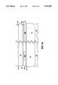
- FIG. 2A cross section of the laser 1 is shown in FIG. 2.
- a left portion of FIG. 2shows a cross section of an exemplary embodiment of the optical amplifiers 3 1-N .
- a right portionshows a cross section of an exemplary embodiment of the passive waveguiding region.
- the laser 1may be grown using SAE.
- the laser 1may be formed in six primary steps as described below.
- a guiding layer 22 of indium-gallium-arsenide-phosphide (InGaAsP)is deposited on a substrate 20 using MOVPE.
- the guiding layer 22provides waveguiding in the vertical direction.
- the guiding layer 22forms a continuously graded region to cover a 1.0 to 1.4 micrometer bandgap, preferably a 1.1 to 1.35 micrometer bandgap.
- the substrate 20may be any material or compound suitable for laser growth, including, without limitation, indium phosphide (InP) or gallium arsenide (GaAs).
- indium phosphideInP
- GaAsgallium arsenide
- MBEmolecular beam epitaxy
- MOMBEmetal organic molecular beam epitaxy
- the layer 24dictates the mode confinement factor of the waveguide.
- the layer 24is preferably about 75 to 225 angstroms thick and may be any alloy composition having a lower refractive index than guiding layer 22 and the ribs 46, discussed below.
- the layer 24is formed from undoped InP.
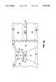
- FIGS. 3b and 3cillustrate the second step of forming the laser 1.
- FIG. 3bis a top view
- FIG. 3cis a cross-sectional view from line aa in FIG. 3b.
- the passive waveguiding region(which is shown on the right side of those figures) is actually located in front of the optical amplifier 3 1-N , occupying the region designated 42 in FIG. 3b. Only the multiquantum well (MQW) material deposited in the region 42 will be patterned, as discussed below, into the passive waveguides.
- MQWmultiquantum well
- a mask 40is deposited on the layer 24 where the optical amplifier 3 will be formed.
- the maskis preferably formed of dielectric material, including, without limitation, SiO x and SiN x .
- the maskis formed from SiO 2 .
- the mask 40can be made by any suitable method such as, without limitation, plasma-assisted chemical vapor deposition, electron beam vaporization or sputtering.
- the material that will patterned into the mask 40is deposited to a thickness of about 3000 angstroms and then etched to create the desired mask configuration.
- the thickness of the mask 40should be about equal to the wavelength of the light used to expose the photoresist during photolithographic patterning. This results in an improvement in mask features, i.e., sharp edges, relative to other thicknesses.
- the mask 40comprises a pair of dielectric rectangles that are spaced to form a gap 41.
- the width of the two strips forming the mask 40, and the gap 41must be sized so that the MQW material grown in the gap is suitable for forming the optically active regions 3 1-N , i.e., has a bandgap wavelength of approximately 1.4-1.6 micrometers, preferably 1.55 micrometers.
- a width of forty micrometers for the strips forming the mask 40, and a gap 41 of fifteen micrometers between the stripshas been found to be suitable for growing MQWs having such a band gap.
- the MQW materialIn areas outside of the mask 40, i.e., outside of the gap 41, the MQW material has a bandgap wavelength of approximately 1.0-1.4 micrometers, preferably 1.35 micrometers, which is suitable for forming the passive waveguides of the laser 1.
- transition regionbetween the nominally 1.55 band gap QW material and 1.35 band gap QW material. This transition region extends a distance of about 1.5 times the gap width moving away from the mask 40 parallel to the gap 41. This region may need to be pumped into transparency. In cases where back reflections are a problem, the transition region may serve as an absorption buffer if power budgets permit.
- the MQW stacks 26a and 26bcomprise a plurality of QW layers. Each QW layer of the stack is separated by a barrier layer.
- the MQW stack 26aincludes barrier layer 63, QW layer 62 and barrier layer 61.
- the QWsshould be tailored to achieve an appropriate compromise between output power, quantum efficiency and bandwidth characteristics.
- the MQW stack 26acomprises five QW layers.
- the MQW stack 26bincludes barrier layer 67, QW layer 66 and barrier layer 65.
- Each QW layer of the MQW stack 26bshould be tailored to maximize optical confinement and provide low loss. Regarding the low loss, free carrier absorption characteristics, scattering and other loss mechanisms should be considered.
- the QWs grown in the gap 41are thicker than those grown outside of it.
- the QWs grown in the gap 41have a higher indium content. This difference in thickness and indium content results in a difference in bandgap energy, and hence, function.
- Two heterostructure confinement layersmay also be deposited to improve mode confinement of the optical amplifier 3 1-N .
- one heterostructure confinement layershould be deposited directly below and above the MQW stack 26a.
- the mask 40is etched away using a suitable etchant such as HF or gas phase chemical etching.
- a stop-etch layer 28is deposited on the MQW stacks 26a and 26b.
- This layerwhich should be about 75 to 225 angstroms thick, is lightly P-doped (about 5 ⁇ 10 15 /cm 3 ) InP.
- a layer 30is then deposited on layer 28. The layer 30 functions as an etch mask to aid, in subsequent etch steps, in sharply defining the passive waveguides of the laser 1.
- Layer 30, which should be about 150 to 450 angstroms thick,is formed of InGaAsP having a bandgap wavelength of about 1.35 micrometers.
- a layer 32is deposited on the layer 30 to insure that the MQW stack 26a is sufficiently buried in a semi-insulating layer 52, discussed below.
- the layer 32also provides lithographic precision in defining the width of the optical amplifier 3.
- the layer 32is about 300 to 900 angstroms thick and is formed of lightly P-doped InP.
- the layer 32is followed by a cap layer 34 to prevent undercut in subsequent etch steps.
- the cap layer 34has a thickness of about 150 to 450 angstroms and is formed of InGaAsP.
- the various layers 28, 30, 32 and 34 that cover the MQW stack 26bare removed, and the wafer undergoes a series of mask and etch steps to pattern the MQW stack 26b in the waveguiding region into ribs 46, as shown on the right side of FIG. 3f.
- These ribswhich should be about 2 to 4 micrometers in width, provide index loading for the underlying slab waveguide 22.
- the ribsare patterned as shown in FIG. 1 to form the passive waveguides that define the optically preferred paths of the laser 1.
- the optical amplifier section 2is protected with a stripe 50 of suitable material, such as SiO 2 .
- step 4a layer 51 of undoped InP, shown in FIG. 3f, is deposited.
- the layer 51decreases the signal loss associated with a current blocking layer 52 that will be deposited next.
- the passive waveguiding region 4is then protected with suitable material, such as SiO 2 and photoresist, which is deposited on layer 51 in preparation for defining the optical amplifiers 3 1-N .
- FIG. 3fshows the optical amplifier 3 patterned into a mesa.
- the stripe 50 that was deposited on top of the cap layer 34acts as a mask while the layers in the optical amplifier region 2 are patterned by a suitable etch into the mesa shape shown in FIG. 3f.
- the mesais preferably about 2 to 4 micrometers high above the bottom of the channel 48 produced by the etch step. Following the etch, the layer 51 is uncovered so that the wafer is delivered for the fifth growth step as shown in FIG. 3f with the mesa top covered by the stripe 50.
- a current blocking layer 52is grown over all exposed surfaces shown in FIG. 3f. This provides current blocking for the optical amplifier 3 and buries the passive waveguides. Current blocking may be achieved by a buried structure such as a reverse biased P-N junction.
- the current blocking layeris preferably formed of Fe doped InP.
- a barrier layer 53 of N-type InPis deposited on the current blocking layer 52. The barrier layer 53 minimizes zinc (P dopant) migration from the layer 54, discussed below, to the layer 52, and iron migration from the layer 52 to the layer 54.
- the stripe 50 and the underlying cap layer 34are then removed from the top of the mesa prior to the last growth step.
- a layer 54is grown over all surfaces to complete the P-contact layer and provide separation of the optical mode from the metal contact subsequently deposited.
- the layer 54is followed by a layer 56 for depositing a ohmic contact, which is preferably a metal such as gold or a gold alloy.
- the layer 54is preferably heavily P-doped InP (about 2 ⁇ 10 18 /cm 3 ) and the layer 56 is preferably even more heavily P- doped InGaAsP (about 5 ⁇ 10 18 /cm 3 ).
- the contact 58is deposited and the facets 13, 15, shown in FIG. 1, are cleaved.
- the facets 13, 15may be appropriately coated so that the facet 13 is substantially totally reflective and the facet 15 is partially 15 transmissive, so that light is emitted by the device 1 at facet 15.
- a single output port 18is provided for light of any wavelength at facet 15.
- the facets 13 and 15are highly reflective except at the output port 18 which is associated with one of the grating arms 12.
- the facet 15is coated with an anti-reflection material 19 so that it is substantially transmissive. There is presently no preference as to which grating arm is selected for location of the output port 18.
- the MQW stacks 26a and 26bare incorporated in the middle of the guiding layer 22, where the optical mode is most intense.
- masks 40are formed and MQW material is deposited.
- the masksare then removed and the balance of the guiding layer 22 is deposited.
- this embodimentrequires altering the relative thickness of some of the layers and further entails using a quaternary layer having a band gap wavelength of about 1.3 micrometers to replace the MQW stack 26b forming the rib 46.
- While a method for forming one optical amplifier 3 1-Nis described above, it should be understood that a plurality of such optical amplifiers 3 1-N and associated waveguides 5 1-N may be formed according to the present invention. In such a case, a plurality of masks 40 would be used to grow a plurality of MQW stacks of suitable bandgap for forming an optical amplifier 3 1-N at a plurality of locations on a substrate.
- the reflective digitally tunable lasermay be formed by cleaving the laser disclosed in U.S. Pat. No. 5,373,517 herein incorporated by reference, in half.
- the wavelength selective device used in the laser described in U.S. Pat. No. 5,373,517may be characterized as a transmissive device, as opposed to the wavelength selective device described herein which is characterized as a reflective device.
- the transmissive deviceincludes two free space regions connected by an optical grating composed of unequal length waveguides. Each free space region is also connected to another plurality of waveguides, equivalent to the waveguides 5 1-N of the present application. Each of these other plurality of waveguides contain optical amplifiers. The optical amplifiers connect these waveguides, located at each end of the transmissive device, to a cleaved facet formed in a wafer on which the aforementioned elements are formed.
- the two cleaved facetscomprise mirrors defining a cavity in which lasing action can be supported.
- a line of symmetryexists through the optical grating of the transmissive device. This line runs perpendicular to the waveguides forming the grating. Cleaving the transmissive device at the line of symmetry yields two mirror image reflective devices.
- the same growth steps used for forming the laser of the present inventionmay be used to form a laser based on the transmissive wavelength selective device.
- a laser based on the transmissive deviceit may be cleaved at the line of symmetry to form two reflective digitally tunable lasers of the present invention.
- An embodiment of the laser 1was formed according to the present invention.
- the entire devicewas fabricated in the six primary steps described above.
- the source materialswere deposited using MOVPE at 100 torr and 615° C. Ethyldimethylindium (10° C.), trimethylgallium (-11° C.), 100 percent arsine and 100 percent phosphine were used as the source materials.
- the substratewas 2 inch ⁇ 100> oriented indium phosphide (InP), heavily S doped at about 10 18 /cm 3 .
- a 4000 angstrom thick guiding layer of InGaAsP having a bandgap wavelength varying from 1.1 to 1.35 micrometerswas deposited on the substrate.
- a layer of undoped InP about 150 angstroms thickwas deposited on the guiding layer.
- step 2twelve SiO 2 masks were deposited on the undoped InP layer at the desired location for the optical amplifiers.
- the SiO 2was deposited to a thickness of about 3000 angstroms and then wet etched through baked photoresist masks using buffered HF to created the desired mask configuration.
- Each maskcomprised a pair of SiO 2 rectangles, each 40 micrometers in width and spaced from one another by 15 micrometers.
- the MQW stackswere grown using SAE.
- the InGaAsP QW layers in the optically active regionwere 95 angstroms thick.
- the InGaAsP barrier layerswere 173 angstroms thick.
- the InGaAsP QW layers in the passive waveguiding regionwere 50 angstroms thick and the InGaAsP barrier layers were 65 angstroms thick.
- Five QW layerswere grown in both the optically active regions and the passive waveguiding regions.
- the maskswere etched away using HF.
- a 150 angstrom thick layer of lightly n-type (about 5 ⁇ 10 15 /cm 3 ) InPwas deposited on the MQW stacks.
- a 300 angstrom thick layer of InGaAsP having a bandgap wavelength of about 1.35 micrometerswas then deposited on the InP layer.
- a 300 angstroms thick cap layer of InGaAsPwas deposited on the InP layer.
- the MQW stacks in the passive waveguiding regionswere uncovered and patterned into 2 to 4 micrometer wide ribs. After the ribs 46 are patterned, the optical amplifier regions were protected with SiO 2 .
- a 3000 angstrom layer of undoped InPwas deposited.
- the passive waveguiding regionswere then protected with SiO 2 and photoresist.
- the optical amplifier regionswere patterned into mesas using a wet chemical HBr etch. The waveguides were then uncovered.
- a Fe doped InP current blocking layertwo microns thick was deposited over all exposed surfaces.
- a 1000 angstrom layer of lightly n-doped InPwas deposited. The strips of SiO 2 , and the cap layer of InGaAsP were removed in preparation for the last growth.
- a layer of heavily Zn doped InP (2 ⁇ 10 18 /cm 3 )was deposited over all surfaces, followed by a layer of more heavily Zn doped InGaAsP (5 ⁇ 10 18 /cm 3 ).
- Gold contactswere deposited over each optical amplifier and the wafer was cleaved at two locations to define the laser cavity.
- the embodiments described hereinare illustrative of the principles of this invention and that various modifications may occur to, and be implemented by those skilled in the art without departing from the scope and spirit of the invention.
- the quantum layers for other devicessuch as modulators, could be deposited in the same QW growth step in which the optical amplifiers and passive waveguides are deposited.
- the method of the present invention for forming a reflective digitally tunable lasercan be used to form a variety of photonic integrated circuits.
Landscapes
- Engineering & Computer Science (AREA)
- Physics & Mathematics (AREA)
- Condensed Matter Physics & Semiconductors (AREA)
- General Physics & Mathematics (AREA)
- Microelectronics & Electronic Packaging (AREA)
- Computer Hardware Design (AREA)
- Manufacturing & Machinery (AREA)
- Power Engineering (AREA)
- Chemical & Material Sciences (AREA)
- Materials Engineering (AREA)
- Electromagnetism (AREA)
- Optics & Photonics (AREA)
- Semiconductor Lasers (AREA)
Abstract
Description
Claims (13)
Priority Applications (4)
| Application Number | Priority Date | Filing Date | Title |
|---|---|---|---|
| US08/308,248US5418183A (en) | 1994-09-19 | 1994-09-19 | Method for a reflective digitally tunable laser |
| CA002155776ACA2155776A1 (en) | 1994-09-19 | 1995-08-10 | Method for a reflective digitally tunable laser |
| EP95306216AEP0702435A1 (en) | 1994-09-19 | 1995-09-06 | Method for making a reflective digitally tunable laser |
| JP7239344AJPH08107251A (en) | 1994-09-19 | 1995-09-19 | Manufacture of reflection digital tuning laser |
Applications Claiming Priority (1)
| Application Number | Priority Date | Filing Date | Title |
|---|---|---|---|
| US08/308,248US5418183A (en) | 1994-09-19 | 1994-09-19 | Method for a reflective digitally tunable laser |
Publications (1)
| Publication Number | Publication Date |
|---|---|
| US5418183Atrue US5418183A (en) | 1995-05-23 |
Family
ID=23193190
Family Applications (1)
| Application Number | Title | Priority Date | Filing Date |
|---|---|---|---|
| US08/308,248Expired - LifetimeUS5418183A (en) | 1994-09-19 | 1994-09-19 | Method for a reflective digitally tunable laser |
Country Status (4)
| Country | Link |
|---|---|
| US (1) | US5418183A (en) |
| EP (1) | EP0702435A1 (en) |
| JP (1) | JPH08107251A (en) |
| CA (1) | CA2155776A1 (en) |
Cited By (37)
| Publication number | Priority date | Publication date | Assignee | Title |
|---|---|---|---|---|
| EP0702435A1 (en)* | 1994-09-19 | 1996-03-20 | AT&T Corp. | Method for making a reflective digitally tunable laser |
| US5659640A (en)* | 1995-06-27 | 1997-08-19 | Lucent Technologies Inc. | Integrated waveguide having an internal optical grating |
| US5698452A (en)* | 1994-04-25 | 1997-12-16 | Lucent Technologies Inc. | Method of making integrated detector/photoemitter with non-imaging director |
| EP0749154A3 (en)* | 1995-06-14 | 1998-05-20 | Mitsubishi Denki Kabushiki Kaisha | Method of fabricating a III-V compound semiconductor layer |
| US5960024A (en)* | 1998-03-30 | 1999-09-28 | Bandwidth Unlimited, Inc. | Vertical optical cavities produced with selective area epitaxy |
| WO2000004616A1 (en)* | 1998-07-18 | 2000-01-27 | The Secretary Of State For Defence | Electro-optic semiconductor devices and method for making the same |
| US6226425B1 (en) | 1999-02-24 | 2001-05-01 | Bandwidth9 | Flexible optical multiplexer |
| US6233263B1 (en) | 1999-06-04 | 2001-05-15 | Bandwidth9 | Monitoring and control assembly for wavelength stabilized optical system |
| US6275513B1 (en) | 1999-06-04 | 2001-08-14 | Bandwidth 9 | Hermetically sealed semiconductor laser device |
| US6366597B1 (en) | 1998-04-14 | 2002-04-02 | Bandwidth9 Inc. | Lattice-relaxed vertical optical cavities |
| US6487230B1 (en) | 1998-04-14 | 2002-11-26 | Bandwidth 9, Inc | Vertical cavity apparatus with tunnel junction |
| US6487231B1 (en) | 1998-04-14 | 2002-11-26 | Bandwidth 9, Inc. | Vertical cavity apparatus with tunnel junction |
| US6493371B1 (en) | 1998-04-14 | 2002-12-10 | Bandwidth9, Inc. | Vertical cavity apparatus with tunnel junction |
| US6493372B1 (en) | 1998-04-14 | 2002-12-10 | Bandwidth 9, Inc. | Vertical cavity apparatus with tunnel junction |
| US6493373B1 (en) | 1998-04-14 | 2002-12-10 | Bandwidth 9, Inc. | Vertical cavity apparatus with tunnel junction |
| US6535541B1 (en) | 1998-04-14 | 2003-03-18 | Bandwidth 9, Inc | Vertical cavity apparatus with tunnel junction |
| US20030081878A1 (en)* | 2001-10-09 | 2003-05-01 | Joyner Charles H. | Transmitter photonic integrated circuit (TxPIC) chip with enhanced power and yield without on-chip amplification |
| US20030095737A1 (en)* | 2001-10-09 | 2003-05-22 | Welch David F. | Transmitter photonic integrated circuits (TxPIC) and optical transport networks employing TxPICs |
| US20030095736A1 (en)* | 2001-10-09 | 2003-05-22 | Kish Fred A. | Transmitter photonic integrated circuit (TxPIC) chip architectures and drive systems and wavelength stabilization for TxPICs |
| US20040033004A1 (en)* | 2001-10-09 | 2004-02-19 | Welch David F. | Optical signal receiver photonic integrated circuit (RxPIC), an associated optical signal transmitter photonic integrated circuit (TxPIC) and an optical network transmission system utilizing these circuits |
| US20040053513A1 (en)* | 1998-05-29 | 2004-03-18 | Osram Opto Semiconductors Gmbh & Co. Ohg, A Regensburg Bavaria, Corporation | Method for production of semiconductor components |
| US6760357B1 (en) | 1998-04-14 | 2004-07-06 | Bandwidth9 | Vertical cavity apparatus with tunnel junction |
| US20040202403A1 (en)* | 2003-04-09 | 2004-10-14 | Lucent Technologies Inc. | Integrated apparatus for processing optical signals |
| US20050111779A1 (en)* | 2002-03-08 | 2005-05-26 | Infinera Corporation | In-wafer testing of integrated optical components in photonic integrated circuits (PICs) |
| US20060263090A1 (en)* | 1999-12-21 | 2006-11-23 | Korea Advanced Institute Of Science And Technology | Low-cost WDM source with an incoherent light injected Fabry-Perot laser diode |
| US20060288933A1 (en)* | 2005-06-27 | 2006-12-28 | Arima Computer Corporation | Chemical vapor deposition reactor |
| US20070274729A1 (en)* | 2003-05-30 | 2007-11-29 | Novera Optics Inc. | Shared High-Intensity Broadband Light Source for a Wavelength-Division Multiple Access Passive Optical Network |
| US20080031626A1 (en)* | 2001-10-09 | 2008-02-07 | Infinera Corporation | Photonic Integrated Circuit (PIC) Chips |
| US20080044128A1 (en)* | 2001-10-09 | 2008-02-21 | Infinera Corporation | TRANSMITTER PHOTONIC INTEGRATED CIRCUITS (TxPICs) AND OPTICAL TRANSPORT NETWORK SYSTEM EMPLOYING TxPICs |
| US20080090316A1 (en)* | 2000-05-30 | 2008-04-17 | Osram Gmbh | Method for manufacture of optically pumped, surface-emitting semiconductor laser device |
| US20080089692A1 (en)* | 2006-10-11 | 2008-04-17 | Novera Optics, Inc. | Mutual wavelength locking in WDM-PONs |
| US20080137698A1 (en)* | 2003-12-19 | 2008-06-12 | Sorin Wayne V | Integration of laser sources and detectors for a passive optical network |
| US20080138088A1 (en)* | 2001-10-09 | 2008-06-12 | Infinera Corporation | Monolithic transmitter photonic integrated circuit (txpic) having tunable modulated sources with feedback system for source power level or wavelength tuning |
| US20090021835A1 (en)* | 2002-10-08 | 2009-01-22 | Infinera Corporation | TILTED COMBINERS/DECOMBINERS AND PHOTONIC INTEGRATED CIRCUITS (PICs) EMPLOYING THE SAME |
| US20090080880A1 (en)* | 2005-09-07 | 2009-03-26 | Chang-Hee Lee | Apparatus for Monitoring Failure Positions in Wavelength Division Multiplexing-Passive Optical Networks and Wavelength Division Multiplexing-Passive Optical Network Systems Having the Apparatus |
| CN101752482B (en)* | 2008-12-17 | 2011-08-31 | 中国科学院半导体研究所 | Growth method of wide-spectrum self-organized quantum dot material |
| US8290370B2 (en) | 2005-09-20 | 2012-10-16 | Korea Advanced Institute Of Science And Technology | Wavelength division multiplexing passive optical network for providing both of broadcasting service and communication service and central office used thereof |
Families Citing this family (1)
| Publication number | Priority date | Publication date | Assignee | Title |
|---|---|---|---|---|
| JP2002344067A (en)* | 2001-05-21 | 2002-11-29 | Sumitomo Electric Ind Ltd | Method for manufacturing optical integrated device |
Citations (7)
| Publication number | Priority date | Publication date | Assignee | Title |
|---|---|---|---|---|
| JPS6077486A (en)* | 1983-10-05 | 1985-05-02 | Matsushita Electric Ind Co Ltd | Manufacturing method of semiconductor laser device |
| US4820655A (en)* | 1986-02-21 | 1989-04-11 | Kokusai Denshin Denwa Kabushiki Kaisha | Method for manufacturing semiconductor optical integrated device with optical waveguide regions |
| US4922500A (en)* | 1989-04-21 | 1990-05-01 | Bell Communications Research, Inc. | Cross-coupled quantum-well stripe laser array |
| EP0411145A1 (en)* | 1989-02-02 | 1991-02-06 | Fujitsu Limited | Integrated optical semiconductor device and method of producing the same |
| US5288659A (en)* | 1988-08-26 | 1994-02-22 | At&T Bell Laboratories | Photonic-integrated-circuit fabrication process |
| US5334551A (en)* | 1991-07-10 | 1994-08-02 | Nec Corporation | Method of making semiconductor optical guided-wave device |
| US5358896A (en)* | 1991-02-25 | 1994-10-25 | Nec Corporation | Method of producing optical integrated circuit |
Family Cites Families (3)
| Publication number | Priority date | Publication date | Assignee | Title |
|---|---|---|---|---|
| DE69407312T2 (en)* | 1993-01-07 | 1998-07-23 | Nippon Electric Co | Integrated semiconductor optical device and manufacturing method |
| DE4304993A1 (en)* | 1993-02-18 | 1994-08-25 | Sel Alcatel Ag | Process for producing a cascaded optical room switch and cascaded optical room switch produced by this process |
| US5418183A (en)* | 1994-09-19 | 1995-05-23 | At&T Corp. | Method for a reflective digitally tunable laser |
- 1994
- 1994-09-19USUS08/308,248patent/US5418183A/ennot_activeExpired - Lifetime
- 1995
- 1995-08-10CACA002155776Apatent/CA2155776A1/ennot_activeAbandoned
- 1995-09-06EPEP95306216Apatent/EP0702435A1/ennot_activeWithdrawn
- 1995-09-19JPJP7239344Apatent/JPH08107251A/ennot_activeWithdrawn
Patent Citations (7)
| Publication number | Priority date | Publication date | Assignee | Title |
|---|---|---|---|---|
| JPS6077486A (en)* | 1983-10-05 | 1985-05-02 | Matsushita Electric Ind Co Ltd | Manufacturing method of semiconductor laser device |
| US4820655A (en)* | 1986-02-21 | 1989-04-11 | Kokusai Denshin Denwa Kabushiki Kaisha | Method for manufacturing semiconductor optical integrated device with optical waveguide regions |
| US5288659A (en)* | 1988-08-26 | 1994-02-22 | At&T Bell Laboratories | Photonic-integrated-circuit fabrication process |
| EP0411145A1 (en)* | 1989-02-02 | 1991-02-06 | Fujitsu Limited | Integrated optical semiconductor device and method of producing the same |
| US4922500A (en)* | 1989-04-21 | 1990-05-01 | Bell Communications Research, Inc. | Cross-coupled quantum-well stripe laser array |
| US5358896A (en)* | 1991-02-25 | 1994-10-25 | Nec Corporation | Method of producing optical integrated circuit |
| US5334551A (en)* | 1991-07-10 | 1994-08-02 | Nec Corporation | Method of making semiconductor optical guided-wave device |
Non-Patent Citations (13)
| Title |
|---|
| Aoki et al., "InGaAs/InGaAsP MQW Electroabsorption-Modulator Integrated with a DFB-Laser Fabricated by Bandgap Energy Control Selective Area MOCVD," Prepublication copy, (Sep. 1994). |
| Aoki et al., InGaAs/InGaAsP MQW Electroabsorption Modulator Integrated with a DFB Laser Fabricated by Bandgap Energy Control Selective Area MOCVD, Prepublication copy, (Sep. 1994).* |
| Caneau et al., "Selective Organometallic Vapor Phase Epitaxy of Ga and In Compounds: A Comparison of TMIn and TEGa versus TMIn and TMGa," J. Cryst. Growth, v. 132, (1993), pp. 364-370. |
| Caneau et al., Selective Organometallic Vapor Phase Epitaxy of Ga and In Compounds: A Comparison of TMIn and TEGa versus TMIn and TMGa, J. Cryst. Growth, v. 132, (1993), pp. 364 370.* |
| Eckel et al., "Improved Composition Homogeneity During Selective Area Epitaxy of GaInAs Using a Novel In Precursor," Appl. Phys. Letts., 64(7), (Feb. 1994), pp. 854-856. |
| Eckel et al., Improved Composition Homogeneity During Selective Area Epitaxy of GaInAs Using a Novel In Precursor, Appl. Phys. Letts., 64(7), (Feb. 1994), pp. 854 856.* |
| Joyner et al., "Extremely Large Band Gap Shifts for MQW Structures by Selective Epitaxy on SiO2 Masked Substrates," IEE Phot. Tech. Letts. 4(9), (Sep. 1992), pp. 1007-1009. |
| Joyner et al., Extremely Large Band Gap Shifts for MQW Structures by Selective Epitaxy on SiO 2 Masked Substrates, IEE Phot. Tech. Letts. 4(9), (Sep. 1992), pp. 1007 1009.* |
| Kato et al., "DFB-LD/Modulator Integrated Light Source by Bandgap Energy Controlled Selective MOVPE," Elect. Letts. 28(2), (Jan. 1992), pp. 153-154. |
| Kato et al., DFB LD/Modulator Integrated Light Source by Bandgap Energy Controlled Selective MOVPE, Elect. Letts. 28(2), (Jan. 1992), pp. 153 154.* |
| Thrush et al., "Selective and Non-Planar Epitaxy of InP, GaInS and GaInAsP Using Low Pressure MOCVD," J. Cryst. Growth, v. 124, (1992), pp. 249-254. |
| Thrush et al., Selective and Non Planar Epitaxy of InP, GaInS and GaInAsP Using Low Pressure MOCVD, J. Cryst. Growth, v. 124, (1992), pp. 249 254.* |
| Zirngibl et al., Digitally Tunable Laser Based on Integration of Waveguide Grating Multiplexer and Optical Amplifier, Elect. Letts., v. 30, (Sep. 1994), p. 701.* |
Cited By (131)
| Publication number | Priority date | Publication date | Assignee | Title |
|---|---|---|---|---|
| US5698452A (en)* | 1994-04-25 | 1997-12-16 | Lucent Technologies Inc. | Method of making integrated detector/photoemitter with non-imaging director |
| EP0702435A1 (en)* | 1994-09-19 | 1996-03-20 | AT&T Corp. | Method for making a reflective digitally tunable laser |
| EP0749154A3 (en)* | 1995-06-14 | 1998-05-20 | Mitsubishi Denki Kabushiki Kaisha | Method of fabricating a III-V compound semiconductor layer |
| US5659640A (en)* | 1995-06-27 | 1997-08-19 | Lucent Technologies Inc. | Integrated waveguide having an internal optical grating |
| US5960024A (en)* | 1998-03-30 | 1999-09-28 | Bandwidth Unlimited, Inc. | Vertical optical cavities produced with selective area epitaxy |
| US6222871B1 (en)* | 1998-03-30 | 2001-04-24 | Bandwidth9 | Vertical optical cavities produced with selective area epitaxy |
| US6487231B1 (en) | 1998-04-14 | 2002-11-26 | Bandwidth 9, Inc. | Vertical cavity apparatus with tunnel junction |
| US6487230B1 (en) | 1998-04-14 | 2002-11-26 | Bandwidth 9, Inc | Vertical cavity apparatus with tunnel junction |
| US6493371B1 (en) | 1998-04-14 | 2002-12-10 | Bandwidth9, Inc. | Vertical cavity apparatus with tunnel junction |
| US6493372B1 (en) | 1998-04-14 | 2002-12-10 | Bandwidth 9, Inc. | Vertical cavity apparatus with tunnel junction |
| US6493373B1 (en) | 1998-04-14 | 2002-12-10 | Bandwidth 9, Inc. | Vertical cavity apparatus with tunnel junction |
| US6535541B1 (en) | 1998-04-14 | 2003-03-18 | Bandwidth 9, Inc | Vertical cavity apparatus with tunnel junction |
| US6366597B1 (en) | 1998-04-14 | 2002-04-02 | Bandwidth9 Inc. | Lattice-relaxed vertical optical cavities |
| US6760357B1 (en) | 1998-04-14 | 2004-07-06 | Bandwidth9 | Vertical cavity apparatus with tunnel junction |
| US6864112B1 (en)* | 1998-05-29 | 2005-03-08 | Osram Opto Semiconductors Gmbh & Co. Ohg | Method of production of a patterned semiconductor layer |
| US6838391B2 (en) | 1998-05-29 | 2005-01-04 | Osram Opto Semiconductors Gmbh & Co. Ohg | Method of semiconductor processing including fluoride |
| US20040053513A1 (en)* | 1998-05-29 | 2004-03-18 | Osram Opto Semiconductors Gmbh & Co. Ohg, A Regensburg Bavaria, Corporation | Method for production of semiconductor components |
| US6630693B1 (en) | 1998-07-18 | 2003-10-07 | Qinetiq Limited | Electro-optic semiconductor devices and method for making the same |
| WO2000004616A1 (en)* | 1998-07-18 | 2000-01-27 | The Secretary Of State For Defence | Electro-optic semiconductor devices and method for making the same |
| US6226425B1 (en) | 1999-02-24 | 2001-05-01 | Bandwidth9 | Flexible optical multiplexer |
| US6275513B1 (en) | 1999-06-04 | 2001-08-14 | Bandwidth 9 | Hermetically sealed semiconductor laser device |
| US6233263B1 (en) | 1999-06-04 | 2001-05-15 | Bandwidth9 | Monitoring and control assembly for wavelength stabilized optical system |
| US8326151B2 (en) | 1999-12-21 | 2012-12-04 | Korea Advanced Institute Of Science And Technology | Low-cost WDM source with an incoherent light injected Fabry-Perot laser diode |
| US20110211839A1 (en)* | 1999-12-21 | 2011-09-01 | Chang Hee Lee | Low-cost wdm source with an incoherent light injected fabry-perot laser diode |
| US20110211838A1 (en)* | 1999-12-21 | 2011-09-01 | Chang Hee Lee | Low-cost wdm source with an incoherent light injected fabry-perot laser diode |
| US8798478B2 (en) | 1999-12-21 | 2014-08-05 | Korea Advanced Institute Of Science And Technology | Low-cost WDM source with an incoherent light injected fabry-perot laser diode |
| US7903979B2 (en) | 1999-12-21 | 2011-03-08 | Korea Advanced Institute Of Science And Technology | Low-cost WDM source with an incoherent light injected Fabry-Perot laser diode |
| US20060263090A1 (en)* | 1999-12-21 | 2006-11-23 | Korea Advanced Institute Of Science And Technology | Low-cost WDM source with an incoherent light injected Fabry-Perot laser diode |
| US8592236B2 (en)* | 2000-05-30 | 2013-11-26 | Osram Gmbh | Method for manufacture of optically pumped, surface-emitting semiconductor laser device |
| US20080090316A1 (en)* | 2000-05-30 | 2008-04-17 | Osram Gmbh | Method for manufacture of optically pumped, surface-emitting semiconductor laser device |
| US7092589B2 (en) | 2001-10-09 | 2006-08-15 | Infinera Corporation | Method of tuning integrated laser sources with integrated wavelength tuning elements on the same substrate or in a monolithic photonic integrated circuit (PIC) |
| US7236656B2 (en) | 2001-10-09 | 2007-06-26 | Infinera Corporation | Optical transport network |
| US20050063636A1 (en)* | 2001-10-09 | 2005-03-24 | Infinera Corporation | Method and apparatus for providing an antireflection coating on the output facet of a photonic integrated circuit (PIC) chip |
| US20050094925A1 (en)* | 2001-10-09 | 2005-05-05 | Infinera Corporation | Method of in-wafer testing of monolithic photonic integrated circuits (PICs) formed in a semiconductor wafer |
| US20050094927A1 (en)* | 2001-10-09 | 2005-05-05 | Infinera Corporation | Probe card for testing in-wafer photonic integrated circuits (PICs) and method of use |
| US20050094926A1 (en)* | 2001-10-09 | 2005-05-05 | Infinera Corporation | Method of calibrating a monolithic transmitter photonic integrated circuit (TxPIC) chip |
| US20050100345A1 (en)* | 2001-10-09 | 2005-05-12 | Infinera Corporation | Monolithic transmitter/receiver photonic integrated circuit (Tx/RxPIC) transceiver chip |
| US9971090B2 (en) | 2001-10-09 | 2018-05-15 | Infinera Corporation | Apparatus and method for tuning a laser source emission wavelength employing a laser source contact comprising electrode segments |
| US20050129350A1 (en)* | 2001-10-09 | 2005-06-16 | Infinera Corporation | Optical transmission network with transmitter photonic integrated circuit (TxPIC) utilizing an optical service channel (OSC) |
| US20050135729A1 (en)* | 2001-10-09 | 2005-06-23 | Welch David F. | Optical transmission network with a receiver photonic integrated circuit (RxPIC) utilizing an optical service chanel (OSC) |
| US20050135778A1 (en)* | 2001-10-09 | 2005-06-23 | Infinera Corporation | Method of providing wider window margin in an eye diagram of a received signal in a transmission system |
| US20050135730A1 (en)* | 2001-10-09 | 2005-06-23 | Infinera Corporation | Method of monitoring and controlling the bit error rate (BER) in an optical communication network |
| US20050135731A1 (en)* | 2001-10-09 | 2005-06-23 | Infinera Corporation | Optical receiver photonic integrated circuit (RxPIC) system |
| US20050201669A1 (en)* | 2001-10-09 | 2005-09-15 | Infinera Corporation | Optical transport network |
| US20050207696A1 (en)* | 2001-10-09 | 2005-09-22 | Infinera Corporation | Compact, cost-effective optical-electrical-optical (OEO) converter for an optical transmission network |
| US20050213883A1 (en)* | 2001-10-09 | 2005-09-29 | Infinera Corporation | Method of optimizing optical channel signal demultiplexing in a monolithic receiver photonic integrated circuit (RxPIC) |
| US20050276613A1 (en)* | 2001-10-09 | 2005-12-15 | Infinera Corporation | FEC enhanced system for an optical communication network |
| US20050286909A1 (en)* | 2001-10-09 | 2005-12-29 | Infinera Corporation | Optical transmitter |
| US6985648B2 (en) | 2001-10-09 | 2006-01-10 | Infinera Corporation | Method of in-wafer testing of monolithic photonic integrated circuits (PICs) formed in a semiconductor wafer |
| US20060023992A1 (en)* | 2001-10-09 | 2006-02-02 | Infinera Corporation | Method of in-wafer testing of monolithic photonic integrated circuits (PICs) formed in a semiconductor wafer |
| US20060062519A1 (en)* | 2001-10-09 | 2006-03-23 | Infinera Corporation | Monolithic photonic integrated circuit (PIC) chip and a method tuning optical components integrated in a monolithic photonic integrated circuit (PIC) |
| US20060067619A1 (en)* | 2001-10-09 | 2006-03-30 | Infinera Corporation | Optical transport network |
| US7043109B2 (en) | 2001-10-09 | 2006-05-09 | Infinera Corporation | Method of in-wafer testing of monolithic photonic integrated circuits (PICs) formed in a semiconductor wafer |
| US7050666B2 (en) | 2001-10-09 | 2006-05-23 | Infinera Corporation | Optical receiver photonic integrated circuit (RxPIC) system |
| US7058246B2 (en) | 2001-10-09 | 2006-06-06 | Infinera Corporation | Transmitter photonic integrated circuit (TxPIC) chip with enhanced power and yield without on-chip amplification |
| US7058263B2 (en) | 2001-10-09 | 2006-06-06 | Infinera Corporation | Optical transport network |
| US7062114B2 (en) | 2001-10-09 | 2006-06-13 | Infinera Corporation | Submount for a photonic integrated circuit (PIC) chip |
| US20030081878A1 (en)* | 2001-10-09 | 2003-05-01 | Joyner Charles H. | Transmitter photonic integrated circuit (TxPIC) chip with enhanced power and yield without on-chip amplification |
| US7079719B2 (en) | 2001-10-09 | 2006-07-18 | Infinera Corporation | Method of tuning optical components integrated on a monolithic chip |
| US7079715B2 (en) | 2001-10-09 | 2006-07-18 | Infinera Corporation | Transmitter photonic integrated circuit (TxPIC) chip architectures and drive systems and wavelength stabilization for TxPICs |
| US7079720B2 (en) | 2001-10-09 | 2006-07-18 | Infinera Corporation | Method of operating an array of laser sources integrated in a monolithic chip or in a photonic integrated circuit (PIC) |
| US7079721B2 (en) | 2001-10-09 | 2006-07-18 | Infinera Corporation | Method and apparatus of monitoring and controlling the emission wavelengths of a plurality of laser sources integrated on the same chip or in the same photonic integrated circuit (PIC) |
| US7079718B2 (en) | 2001-10-09 | 2006-07-18 | Infinera Corporation | Optical probe and method of testing employing an interrogation beam or optical pickup |
| US7082253B2 (en) | 2001-10-09 | 2006-07-25 | Infinera Corporation | Method of providing wider window margin in an eye diagram of a received signal in a transmission system |
| US20050018720A1 (en)* | 2001-10-09 | 2005-01-27 | Infinera Corporation | Contact length trimming or vernier resistor trimming of a semiconductor laser source contact to change the source applied current density and resulting operational wavelength |
| US7103239B2 (en) | 2001-10-09 | 2006-09-05 | Infinera Corporation | Optical transmitter |
| US7113667B2 (en) | 2001-10-09 | 2006-09-26 | Infinera Corporation | FEC enhanced system for an optical communication network |
| US7116851B2 (en) | 2001-10-09 | 2006-10-03 | Infinera Corporation | Optical signal receiver, an associated photonic integrated circuit (RxPIC), and method improving performance |
| US7116861B2 (en) | 2001-10-09 | 2006-10-03 | Infinera Corporation | Method of monitoring and controlling the bit error rate (BER) in an optical communication network |
| US20060228067A1 (en)* | 2001-10-09 | 2006-10-12 | Infinera Corporation | Method of manufacturing and apparatus for a transmitter photonic integrated circuit (TXPIC) chip |
| US7123786B2 (en) | 2001-10-09 | 2006-10-17 | Infinera Corporation | Compact, cost-effective optical-electrical-optical (OEO) converter for an optical transmission network |
| US20030095737A1 (en)* | 2001-10-09 | 2003-05-22 | Welch David F. | Transmitter photonic integrated circuits (TxPIC) and optical transport networks employing TxPICs |
| US7136546B2 (en) | 2001-10-09 | 2006-11-14 | Infinera Corporation | Method and apparatus of monitoring and controlling the emission wavelengths of a plurality of laser sources integrated on the same chip or in the same photonic integrated circuit (PIC) |
| US20050014300A1 (en)* | 2001-10-09 | 2005-01-20 | Infinera Corporation | Optical probe and method of testing employing an interrogation beam or optical pickup |
| US7155078B2 (en) | 2001-10-09 | 2006-12-26 | Infinera Corporation | Optical transmission network with transmitter photonic integrated circuit (TxPIC) utilizing an optical service channel (OSC) |
| US20030095736A1 (en)* | 2001-10-09 | 2003-05-22 | Kish Fred A. | Transmitter photonic integrated circuit (TxPIC) chip architectures and drive systems and wavelength stabilization for TxPICs |
| US7158699B2 (en) | 2001-10-09 | 2007-01-02 | Infinera Corporation | Method of optimizing optical channel signal demultiplexing in a monolithic receiver photonic integrated circuit (RxPIC) |
| US20070019901A1 (en)* | 2001-10-09 | 2007-01-25 | Infinera Corporation | Method tuning optical components integrated in a monolithic photonic integrated circuit (PIC) |
| US7200296B2 (en) | 2001-10-09 | 2007-04-03 | Infinera Corporation | Monolithic photonic integrated circuit (PIC) CHIP |
| US7224858B2 (en) | 2001-10-09 | 2007-05-29 | Infinera Corporation | Optical transmission network with a receiver photonic integrated circuit (RxPIC) utilizing an optical service chanel (OSC) |
| US20070122148A1 (en)* | 2001-10-09 | 2007-05-31 | Infinera Corporation | Method of monitoring and controlling the bit error rate (ber) in an optical communication network |
| US20050025409A1 (en)* | 2001-10-09 | 2005-02-03 | Infinera Corporation | Submount for a photonic integrated circuit (PIC) chip |
| US20070172169A1 (en)* | 2001-10-09 | 2007-07-26 | Infinera Corporation | Method of tuning optical components integrated in a monolithic photonic integrated circuit (pic) |
| US7283694B2 (en) | 2001-10-09 | 2007-10-16 | Infinera Corporation | Transmitter photonic integrated circuits (TxPIC) and optical transport networks employing TxPICs |
| US20070242918A1 (en)* | 2001-10-09 | 2007-10-18 | Infinera Corporation | Transmitter Photonic Integrated Circuits (TxPICs) with Directly Modulated Lasers and Wavelength Selective Combiners |
| US20070248299A1 (en)* | 2001-10-09 | 2007-10-25 | Infinera Corporation | Monolithic Transmitter Photonic Integrated Circuit (TxPIC) Semiconductor Chip |
| US20040033004A1 (en)* | 2001-10-09 | 2004-02-19 | Welch David F. | Optical signal receiver photonic integrated circuit (RxPIC), an associated optical signal transmitter photonic integrated circuit (TxPIC) and an optical network transmission system utilizing these circuits |
| US7324719B2 (en) | 2001-10-09 | 2008-01-29 | Infinera Corporation | Method tuning optical components integrated in a monolithic photonic integrated circuit (PIC) |
| US20080031626A1 (en)* | 2001-10-09 | 2008-02-07 | Infinera Corporation | Photonic Integrated Circuit (PIC) Chips |
| US20080044128A1 (en)* | 2001-10-09 | 2008-02-21 | Infinera Corporation | TRANSMITTER PHOTONIC INTEGRATED CIRCUITS (TxPICs) AND OPTICAL TRANSPORT NETWORK SYSTEM EMPLOYING TxPICs |
| US20050013332A1 (en)* | 2001-10-09 | 2005-01-20 | Infinera Corporation | Method and apparatus of monitoring and controlling the emission wavelengths of a plurality of laser sources integrated on the same chip or in the same photonic integrated circuit (PIC) |
| US20040067006A1 (en)* | 2001-10-09 | 2004-04-08 | Welch David F. | Transmitter photonic integrated circuit ( TxPIC) chips |
| US7885492B2 (en) | 2001-10-09 | 2011-02-08 | Infinera Corporation | Transmitter photonic integrated circuit (TxPIC) chips |
| US20080138088A1 (en)* | 2001-10-09 | 2008-06-12 | Infinera Corporation | Monolithic transmitter photonic integrated circuit (txpic) having tunable modulated sources with feedback system for source power level or wavelength tuning |
| US7437029B2 (en) | 2001-10-09 | 2008-10-14 | Infinera Corporation | Method of manufacturing and apparatus for a transmitter photonic integrated circuit (TXPIC) chip |
| US7460742B2 (en) | 2001-10-09 | 2008-12-02 | Infinera Corporation | Method and apparatus for providing an antireflection coating on the output facet of a photonic integrated circuit (PIC) chip |
| US7466882B2 (en) | 2001-10-09 | 2008-12-16 | Infinera Corporation | Monolithic transmitter/receiver photonic integrated circuit (Tx/RxPIC) transceiver chip |
| US7471857B2 (en) | 2001-10-09 | 2008-12-30 | Infinera Corporation | Method of tuning optical components integrated in a monolithic photonic integrated circuit (PIC) |
| US7477807B2 (en) | 2001-10-09 | 2009-01-13 | Infinera Corporation | Monolithic transmitter photonic integrated circuit (TxPIC) semiconductor chip |
| US7792396B2 (en) | 2001-10-09 | 2010-09-07 | Infinera Corporation | Probe card for testing in-wafer photonic integrated circuits (PICs) and method of use |
| US7483599B2 (en) | 2001-10-09 | 2009-01-27 | Infinera Corporation | Method of calibrating a monolithic transmitter photonic integrated circuit (TXPIC) chip |
| US7489838B2 (en) | 2001-10-09 | 2009-02-10 | Infinera Corporation | Optical transmitter |
| US7751658B2 (en) | 2001-10-09 | 2010-07-06 | Infinera Corporation | Monolithic transmitter photonic integrated circuit (TxPIC) having tunable modulated sources with feedback system for source power level or wavelength tuning |
| US7519246B2 (en) | 2001-10-09 | 2009-04-14 | Infinera Corporation | Photonic integrated circuit (PIC) chips |
| US7680368B2 (en) | 2001-10-09 | 2010-03-16 | Infinera Corporation | Monolithic transmitter photonic integrated circuit (TxPIC) with a traversely disposed output |
| US7546001B2 (en) | 2001-10-09 | 2009-06-09 | Infinera Corporation | Monolithic photonic integrated circuit (PIC) with forward error correction (FEC) |
| US7551815B2 (en) | 2001-10-09 | 2009-06-23 | Infinera Corporation | Method of monitoring and controlling the bit error rate (BER) in an optical communication network |
| US7672546B2 (en) | 2001-10-09 | 2010-03-02 | Infinera Corporation | Optical transport network having a plurality of monolithic photonic integrated circuit semiconductor chips |
| US20050111779A1 (en)* | 2002-03-08 | 2005-05-26 | Infinera Corporation | In-wafer testing of integrated optical components in photonic integrated circuits (PICs) |
| US7529436B2 (en) | 2002-03-08 | 2009-05-05 | Infinera Corporation | Optical combiner/decombiner with reduced insertion loss |
| US20060138433A1 (en)* | 2002-03-08 | 2006-06-29 | Infinera Corporation | Optical combiner/decombiner with reduced insertion loss |
| US7135382B2 (en)* | 2002-03-08 | 2006-11-14 | Infinera Corporation | In-wafer testing of integrated optical components in photonic integrated circuits (PICs) |
| US7747114B2 (en) | 2002-10-08 | 2010-06-29 | Infinera Corporation | Tilted combiners/decombiners and photonic integrated circuits (PICs) employing the same |
| US20090021835A1 (en)* | 2002-10-08 | 2009-01-22 | Infinera Corporation | TILTED COMBINERS/DECOMBINERS AND PHOTONIC INTEGRATED CIRCUITS (PICs) EMPLOYING THE SAME |
| US20040202403A1 (en)* | 2003-04-09 | 2004-10-14 | Lucent Technologies Inc. | Integrated apparatus for processing optical signals |
| US20070274729A1 (en)* | 2003-05-30 | 2007-11-29 | Novera Optics Inc. | Shared High-Intensity Broadband Light Source for a Wavelength-Division Multiple Access Passive Optical Network |
| US8861963B2 (en) | 2003-05-30 | 2014-10-14 | Novera Optics, Inc. | Shared high-intensity broadband light source for a wavelength-division multiple access passive optical network |
| US7944960B2 (en) | 2003-12-19 | 2011-05-17 | Novera Optics, Inc. | Integration of laser sources and detectors for a passive optical network |
| US20100014865A1 (en)* | 2003-12-19 | 2010-01-21 | Sorin Wayne V | Integration of laser sources and detectors for a passive optical network |
| EP1695466B1 (en)* | 2003-12-19 | 2011-06-08 | Novera Optics, Inc. | Integration of laser sources and detectors for a passive optical network |
| US7593444B2 (en) | 2003-12-19 | 2009-09-22 | Novera Optics, Inc. | Integration of laser sources and detectors for a passive optical network |
| EP2259454A1 (en)* | 2003-12-19 | 2010-12-08 | Novera Optics, Inc. | Integration of laser sources and detectors for a passive optical network |
| US7916767B2 (en) | 2003-12-19 | 2011-03-29 | Novera Optics, Inc. | Integration of laser sources and detectors for a passive optical network |
| US20080137698A1 (en)* | 2003-12-19 | 2008-06-12 | Sorin Wayne V | Integration of laser sources and detectors for a passive optical network |
| US20060288933A1 (en)* | 2005-06-27 | 2006-12-28 | Arima Computer Corporation | Chemical vapor deposition reactor |
| US20090080880A1 (en)* | 2005-09-07 | 2009-03-26 | Chang-Hee Lee | Apparatus for Monitoring Failure Positions in Wavelength Division Multiplexing-Passive Optical Networks and Wavelength Division Multiplexing-Passive Optical Network Systems Having the Apparatus |
| US9130671B2 (en) | 2005-09-07 | 2015-09-08 | Korea Advanced Institute Of Science And Technology | Apparatus for monitoring failure positions in wavelength division multiplexing-passive optical networks and wavelength division multiplexing-passive optical network systems having the apparatus |
| US8290370B2 (en) | 2005-09-20 | 2012-10-16 | Korea Advanced Institute Of Science And Technology | Wavelength division multiplexing passive optical network for providing both of broadcasting service and communication service and central office used thereof |
| US8571410B2 (en) | 2006-10-11 | 2013-10-29 | Novera Optics, Inc. | Mutual wavelength locking in WDM-PONS |
| US20080089692A1 (en)* | 2006-10-11 | 2008-04-17 | Novera Optics, Inc. | Mutual wavelength locking in WDM-PONs |
| CN101752482B (en)* | 2008-12-17 | 2011-08-31 | 中国科学院半导体研究所 | Growth method of wide-spectrum self-organized quantum dot material |
Also Published As
| Publication number | Publication date |
|---|---|
| CA2155776A1 (en) | 1996-03-20 |
| JPH08107251A (en) | 1996-04-23 |
| EP0702435A1 (en) | 1996-03-20 |
Similar Documents
| Publication | Publication Date | Title |
|---|---|---|
| US5418183A (en) | Method for a reflective digitally tunable laser | |
| US5659640A (en) | Integrated waveguide having an internal optical grating | |
| US7941024B2 (en) | Buried heterostructure device having integrated waveguide grating fabricated by single step MOCVD | |
| JP3285426B2 (en) | Semiconductor optical integrated device and method of manufacturing the same | |
| JPS6215875A (en) | Semiconductor device and its manufacturing method | |
| US6383829B1 (en) | Optical semiconductor device and method of fabricating the same | |
| JPH0381317B2 (en) | ||
| US5042049A (en) | Semiconductor optical device | |
| EP0680119B1 (en) | Fabrication process for semiconductor optical device | |
| JPH0864906A (en) | Manufacturing method of semiconductor device | |
| US5847415A (en) | Light emitting device having current blocking structure | |
| JP2001148531A (en) | Semiconductor optical device | |
| JP4194844B2 (en) | Semiconductor laser with multiple optically active regions | |
| US5756373A (en) | Method for fabricating optical semiconductor device | |
| US7184640B2 (en) | Buried heterostructure device fabricated by single step MOCVD | |
| CN115280609B (en) | Optics | |
| EP4122062B1 (en) | Electroabsorption modulated laser | |
| JPH077232A (en) | Optical semiconductor device | |
| EP0528439A1 (en) | Semiconductor laser | |
| JPH08292336A (en) | Production of optical semiconductor integrated circuit | |
| JP3251615B2 (en) | Semiconductor laser device | |
| JPH1140885A (en) | Semiconductor laser device | |
| JPH08288583A (en) | Semiconductor optical device and manufacturing method thereof | |
| Xie et al. | Integration of GaAs/AlGaAs SQW laser and MQW modulator via a tapered waveguide interconnect without regrowth |
Legal Events
| Date | Code | Title | Description |
|---|---|---|---|
| AS | Assignment | Owner name:AT&T CORP. 32 AVENUE OF THE AMERICAS Free format text:ASSIGNMENT OF ASSIGNORS INTEREST;ASSIGNORS:JOYNER, CHARLES H.;MEESTER, JUDITH P.;ZIRNGIBL, MARTIN;REEL/FRAME:007157/0295 Effective date:19940914 | |
| STCF | Information on status: patent grant | Free format text:PATENTED CASE | |
| FEPP | Fee payment procedure | Free format text:PAYOR NUMBER ASSIGNED (ORIGINAL EVENT CODE: ASPN); ENTITY STATUS OF PATENT OWNER: LARGE ENTITY | |
| FPAY | Fee payment | Year of fee payment:4 | |
| FPAY | Fee payment | Year of fee payment:8 | |
| REMI | Maintenance fee reminder mailed | ||
| FPAY | Fee payment | Year of fee payment:12 | |
| AS | Assignment | Owner name:DEUTSCHE BANK AG NEW YORK BRANCH, AS COLLATERAL AG Free format text:PATENT SECURITY AGREEMENT;ASSIGNORS:LSI CORPORATION;AGERE SYSTEMS LLC;REEL/FRAME:032856/0031 Effective date:20140506 | |
| AS | Assignment | Owner name:AVAGO TECHNOLOGIES GENERAL IP (SINGAPORE) PTE. LTD Free format text:ASSIGNMENT OF ASSIGNORS INTEREST;ASSIGNOR:AGERE SYSTEMS LLC;REEL/FRAME:035365/0634 Effective date:20140804 | |
| AS | Assignment | Owner name:AGERE SYSTEMS LLC, PENNSYLVANIA Free format text:TERMINATION AND RELEASE OF SECURITY INTEREST IN PATENT RIGHTS (RELEASES RF 032856-0031);ASSIGNOR:DEUTSCHE BANK AG NEW YORK BRANCH, AS COLLATERAL AGENT;REEL/FRAME:037684/0039 Effective date:20160201 Owner name:LSI CORPORATION, CALIFORNIA Free format text:TERMINATION AND RELEASE OF SECURITY INTEREST IN PATENT RIGHTS (RELEASES RF 032856-0031);ASSIGNOR:DEUTSCHE BANK AG NEW YORK BRANCH, AS COLLATERAL AGENT;REEL/FRAME:037684/0039 Effective date:20160201 |