US5416043A - Minimum charge FET fabricated on an ultrathin silicon on sapphire wafer - Google Patents
Minimum charge FET fabricated on an ultrathin silicon on sapphire waferDownload PDFInfo
- Publication number
- US5416043A US5416043AUS08/090,400US9040093AUS5416043AUS 5416043 AUS5416043 AUS 5416043AUS 9040093 AUS9040093 AUS 9040093AUS 5416043 AUS5416043 AUS 5416043A
- Authority
- US
- United States
- Prior art keywords
- silicon
- layer
- approximately
- sapphire
- sapphire substrate
- Prior art date
- Legal status (The legal status is an assumption and is not a legal conclusion. Google has not performed a legal analysis and makes no representation as to the accuracy of the status listed.)
- Expired - Lifetime
Links
Images


Classifications
- H—ELECTRICITY
- H10—SEMICONDUCTOR DEVICES; ELECTRIC SOLID-STATE DEVICES NOT OTHERWISE PROVIDED FOR
- H10D—INORGANIC ELECTRIC SEMICONDUCTOR DEVICES
- H10D1/00—Resistors, capacitors or inductors
- H10D1/40—Resistors
- H10D1/47—Resistors having no potential barriers
- H—ELECTRICITY
- H01—ELECTRIC ELEMENTS
- H01L—SEMICONDUCTOR DEVICES NOT COVERED BY CLASS H10
- H01L21/00—Processes or apparatus adapted for the manufacture or treatment of semiconductor or solid state devices or of parts thereof
- H01L21/02—Manufacture or treatment of semiconductor devices or of parts thereof
- H01L21/02104—Forming layers
- H01L21/02365—Forming inorganic semiconducting materials on a substrate
- H01L21/02367—Substrates
- H01L21/0237—Materials
- H01L21/0242—Crystalline insulating materials
- H—ELECTRICITY
- H01—ELECTRIC ELEMENTS
- H01L—SEMICONDUCTOR DEVICES NOT COVERED BY CLASS H10
- H01L21/00—Processes or apparatus adapted for the manufacture or treatment of semiconductor or solid state devices or of parts thereof
- H01L21/02—Manufacture or treatment of semiconductor devices or of parts thereof
- H01L21/02104—Forming layers
- H01L21/02365—Forming inorganic semiconducting materials on a substrate
- H01L21/02518—Deposited layers
- H01L21/02521—Materials
- H01L21/02524—Group 14 semiconducting materials
- H01L21/02532—Silicon, silicon germanium, germanium
- H—ELECTRICITY
- H01—ELECTRIC ELEMENTS
- H01L—SEMICONDUCTOR DEVICES NOT COVERED BY CLASS H10
- H01L21/00—Processes or apparatus adapted for the manufacture or treatment of semiconductor or solid state devices or of parts thereof
- H01L21/02—Manufacture or treatment of semiconductor devices or of parts thereof
- H01L21/02104—Forming layers
- H01L21/02365—Forming inorganic semiconducting materials on a substrate
- H01L21/02656—Special treatments
- H01L21/02664—Aftertreatments
- H01L21/02694—Controlling the interface between substrate and epitaxial layer, e.g. by ion implantation followed by annealing
- H—ELECTRICITY
- H01—ELECTRIC ELEMENTS
- H01L—SEMICONDUCTOR DEVICES NOT COVERED BY CLASS H10
- H01L21/00—Processes or apparatus adapted for the manufacture or treatment of semiconductor or solid state devices or of parts thereof
- H01L21/70—Manufacture or treatment of devices consisting of a plurality of solid state components formed in or on a common substrate or of parts thereof; Manufacture of integrated circuit devices or of parts thereof
- H01L21/71—Manufacture of specific parts of devices defined in group H01L21/70
- H01L21/76—Making of isolation regions between components
- H01L21/762—Dielectric regions, e.g. EPIC dielectric isolation, LOCOS; Trench refilling techniques, SOI technology, use of channel stoppers
- H01L21/7624—Dielectric regions, e.g. EPIC dielectric isolation, LOCOS; Trench refilling techniques, SOI technology, use of channel stoppers using semiconductor on insulator [SOI] technology
- H01L21/76264—SOI together with lateral isolation, e.g. using local oxidation of silicon, or dielectric or polycristalline material refilled trench or air gap isolation regions, e.g. completely isolated semiconductor islands
- H—ELECTRICITY
- H10—SEMICONDUCTOR DEVICES; ELECTRIC SOLID-STATE DEVICES NOT OTHERWISE PROVIDED FOR
- H10B—ELECTRONIC MEMORY DEVICES
- H10B10/00—Static random access memory [SRAM] devices
- H10B10/15—Static random access memory [SRAM] devices comprising a resistor load element
- H—ELECTRICITY
- H10—SEMICONDUCTOR DEVICES; ELECTRIC SOLID-STATE DEVICES NOT OTHERWISE PROVIDED FOR
- H10D—INORGANIC ELECTRIC SEMICONDUCTOR DEVICES
- H10D30/00—Field-effect transistors [FET]
- H10D30/60—Insulated-gate field-effect transistors [IGFET]
- H10D30/67—Thin-film transistors [TFT]
- H10D30/6704—Thin-film transistors [TFT] having supplementary regions or layers in the thin films or in the insulated bulk substrates for controlling properties of the device
- H10D30/6713—Thin-film transistors [TFT] having supplementary regions or layers in the thin films or in the insulated bulk substrates for controlling properties of the device characterised by the properties of the source or drain regions, e.g. compositions or sectional shapes
- H10D30/6715—Thin-film transistors [TFT] having supplementary regions or layers in the thin films or in the insulated bulk substrates for controlling properties of the device characterised by the properties of the source or drain regions, e.g. compositions or sectional shapes characterised by the doping profiles, e.g. having lightly-doped source or drain extensions
- H—ELECTRICITY
- H10—SEMICONDUCTOR DEVICES; ELECTRIC SOLID-STATE DEVICES NOT OTHERWISE PROVIDED FOR
- H10D—INORGANIC ELECTRIC SEMICONDUCTOR DEVICES
- H10D30/00—Field-effect transistors [FET]
- H10D30/60—Insulated-gate field-effect transistors [IGFET]
- H10D30/67—Thin-film transistors [TFT]
- H10D30/674—Thin-film transistors [TFT] characterised by the active materials
- H10D30/6741—Group IV materials, e.g. germanium or silicon carbide
- H10D30/6743—Silicon
- H10D30/6744—Monocrystalline silicon
- H—ELECTRICITY
- H10—SEMICONDUCTOR DEVICES; ELECTRIC SOLID-STATE DEVICES NOT OTHERWISE PROVIDED FOR
- H10D—INORGANIC ELECTRIC SEMICONDUCTOR DEVICES
- H10D30/00—Field-effect transistors [FET]
- H10D30/60—Insulated-gate field-effect transistors [IGFET]
- H10D30/67—Thin-film transistors [TFT]
- H10D30/6758—Thin-film transistors [TFT] characterised by the insulating substrates
- H10D30/6759—Silicon-on-sapphire [SOS] substrates
- H—ELECTRICITY
- H10—SEMICONDUCTOR DEVICES; ELECTRIC SOLID-STATE DEVICES NOT OTHERWISE PROVIDED FOR
- H10D—INORGANIC ELECTRIC SEMICONDUCTOR DEVICES
- H10D86/00—Integrated devices formed in or on insulating or conducting substrates, e.g. formed in silicon-on-insulator [SOI] substrates or on stainless steel or glass substrates
- H10D86/201—Integrated devices formed in or on insulating or conducting substrates, e.g. formed in silicon-on-insulator [SOI] substrates or on stainless steel or glass substrates the substrates comprising an insulating layer on a semiconductor body, e.g. SOI
- H—ELECTRICITY
- H01—ELECTRIC ELEMENTS
- H01L—SEMICONDUCTOR DEVICES NOT COVERED BY CLASS H10
- H01L21/00—Processes or apparatus adapted for the manufacture or treatment of semiconductor or solid state devices or of parts thereof
- H01L21/70—Manufacture or treatment of devices consisting of a plurality of solid state components formed in or on a common substrate or of parts thereof; Manufacture of integrated circuit devices or of parts thereof
- H01L21/71—Manufacture of specific parts of devices defined in group H01L21/70
- H01L21/76—Making of isolation regions between components
- H01L21/762—Dielectric regions, e.g. EPIC dielectric isolation, LOCOS; Trench refilling techniques, SOI technology, use of channel stoppers
- H01L21/7624—Dielectric regions, e.g. EPIC dielectric isolation, LOCOS; Trench refilling techniques, SOI technology, use of channel stoppers using semiconductor on insulator [SOI] technology
- H01L21/76264—SOI together with lateral isolation, e.g. using local oxidation of silicon, or dielectric or polycristalline material refilled trench or air gap isolation regions, e.g. completely isolated semiconductor islands
- H01L21/76281—Lateral isolation by selective oxidation of silicon
Definitions
- the current inventionrelates generally to the fabrication of semiconductor-on-insulator composite substrates, such as silicon-on-sapphire (SOS), and more particularly to devices, structures and processes for providing transistors in integrated circuits in silicon-on-sapphire material.
- semiconductor-on-insulator composite substratessuch as silicon-on-sapphire (SOS)
- SOSsilicon-on-sapphire
- the field effect transistorcontrols current conduction from a source region to a drain region by application of voltage to a gate conductor. If the gate conductor is insulated from the source-drain conduction channel, the device is called an insulated gate FET.
- the most common gate structureis that of metal oxide semiconductor, or the MOSFET.
- MOSFETmetal oxide semiconductor
- fixed chargeDopant atoms and electrically active states (hereinafter called “fixed charge”) in the conduction channel region of MOSFETs are charged and discharged during operation of the device. Since fixed charge is immobile, it does not contribute to FET current conduction. Therefore, the charging and discharging of fixed charges introduces parasitic charge to the transistor with many negative effects, including scattering of conduction carriers; variation in threshold voltage; introduction of buried channel operation; introduction of a body effect; complication of device modeling; increased complexity for device and process design; increased electric fields; and difficulty in scaling devices to smaller dimensions or voltages, among others.
- Dopant atomsare introduced into MOSFETs for specific reasons such as to adjust threshold voltage or to control substrate currents, with the aforementioned adverse side effects accepted as necessary by-products of dopant atom introduction. It would be very desirable to be able to introduce only the specific type, quantity and location of dopant atoms which are necessary to achieve the desired electrical characteristics for the device and to avoid or eliminate all other dopant atoms.
- the "ideal" semiconductor materialwould thus include a completely monocrystalline, defect-free silicon layer of sufficient thickness to accommodate the fabrication of active devices thereon. Ideal operation of MOSFETs would occur if there were no parasitic charge (which we define as unintended or excess dopant atoms plus electrically active states) in the conduction channel.
- threshold voltageis the gate voltage necessary to initiate conduction.
- a common technique for setting threshold voltageis to modify the dopant concentrations in the channel region.
- this approachhas the undesirable side effects associated with dopant charge mentioned above.
- adjusting threshold voltage by ion implantationrequires at least two and often four masking steps which increase cost and decrease yield.
- silicon-on-sapphirehas been used for high performance MOSFET microelectronics, primarily for applications requiring radiation hardness.
- a silicon filmis epitaxially grown on a sapphire substrate.
- the silicon filmis thin compared to the source to drain separation (called the channel length) and the insulating substrate is thick enough to ensure no significant electrostatic coupling to a back plane. Due to crystal and thermal expansion mismatches between the silicon and the sapphire, the silicon films are typically heavily populated with crystalline defects and electrically active states. The dominant type of crystalline defects are commonly called "twins".
- the quality of the silicon filmscan be improved by increasing the thickness of the silicon, hence traditional SOS is made with silicon films between 400 and 800 nanometers thick. This film thickness is capable of supporting transistors with channel lengths down to about 1 micron. Submicron channel length devices cannot be made in traditional SOS materials as thinner films are required.
- a composite substratecomprised of a monocrystalline semiconductor layer, such as silicon, epitaxially deposited on a supporting insulative substrate are well recognized. These advantages include the substantial reduction of parasitic capacitance between charged active regions and the substrate and the effective elimination of leakage currents flowing between adjacent active devices. This is accomplished by employing as the substrate an insulative material, such as sapphire (Al 2 O 3 ), and providing that the conduction path of any interdevice leakage current must pass through the substrate.
- An "ideal" silicon-on-sapphire wafermay be defined to include a completely monocrystalline, defect-free silicon layer of sufficient thickness to accommodate the fabrication of active devices therein.
- the silicon layerwould be adjacent to a sapphire substrate and would have a minimum of crystal lattice discontinuities at the silicon-sapphire interface.
- Previous attempts to fabricate this "ideal" silicon-on-sapphire (SOS) waferhave been frustrated by a number of significant problems.
- the first significant problem encountered in attempts to fabricate the ideal SOS waferwas the substantial incursion of contaminants into the epitaxially deposited silicon layer.
- substantial concentrations of aluminum contaminants, diffused from the sapphire substrate,were found throughout the silicon epitaxial layer.
- MOSFETsMetal Oxide Semiconductor Field Effect Transistor
- MESFETsMetal Semiconductor FET
- the SPE processprovides a low temperature subprocess for improving the crystallinity of the silicon epitaxial layer of a silicon-on-sapphire composite substrate.
- the SPE processinvolves the high energy implantation (typically at 40 KeV to 550 KeV) of an ion species, such as silicon, into the silicon epitaxial layer at a sufficient dose (typically 10 15 to 10 16 ions/cm 2 ) to create a substantially amorphous silicon layer lying adjacent the silicon/sapphire interface while leaving a substantially crystalline layer at the surface of the original epitaxial layer.
- the thickness of the silicon epitaxial layeris substantially that intended for the completed silicon-on-sapphire composite substrate (typically 3000 ⁇ -6000 ⁇ ).
- the ion speciesis implanted through the majority of the epitaxial layer so that the maximum disruption of the silicon crystal lattice is near, but not across, the silicon/sapphire interface to ensure that the amorphous region is adjacent the sapphire substrate.
- the sapphire substrateis kept below about 100° C. by cooling with Freon or liquid Nitrogen.
- a single step low temperature (600° C.) annealing of the composite substrateis then performed to convert the amorphous silicon layer into crystalline silicon. During this regrowth, the remaining crystalline surface portion of the silicon layer effectively acts as a nucleation seed so that the regrown portion of the silicon epitaxial layer has a common crystallographic orientation and is substantially free of crystalline defects.
- Lau's SPE processdoes significantly improve the crystallinity of the silicon epitaxial layer, it also facilitates the diffusion of aluminum from the sapphire substrate (Al 2 O 3 ) into the silicon epitaxial layer, which dopes the silicon film P-type.
- the contaminant concentration resulting from the use of the SPE processis, unfortunately, sufficient to preclude the practical use of integrated circuits fabricated on composite substrates processed with this SPE subprocess.
- the reasons for the failure of active devices to operate correctlyare essentially the same as given above with regard to composite substrates fabricated utilizing high temperature processing steps. Additionally, it has been observed that the method described by Lau et al., can leave enough electrically active states in the silicon epitaxial layer to preclude its use for fabrication of integrated circuits.
- U.S. Pat. No. 4,509,990entitled "SOLID PHASE EPITAXY AND REGROWTH PROCESS WITH CONTROLLED DEFECT DENSITY PROFILING FOR HETEROEPITAXIAL SEMICONDUCTOR ON INSULATOR COMPOSITE SUBSTRATES", issued to Vasudev, also describes use of ion implantation and solid phase regrowth to prepare a silicon-on-sapphire wafer.
- a method for fabricating a silicon-on-sapphire wafer very similar to that taught by Lau et al.is described with the additional requirement that the implantation energy and the ion dose are constrained such that they are sufficiently low so as not to exceed the damage density threshold of the sapphire substrate.
- the methoddescribes a residual high defect density in the silicon layer near the sapphire substrate.
- Both embodimentsutilize a method for controlling the temperature of the rear surface of the sapphire substrate by mounting the substrate on a heat sink with either a thin film of thermal paste or a thin film of silicon positioned intermediate to the rear surface of the substrate and the heat sink to provide a high heat conductivity interface therebetween.
- the temperature of the heat sinkis held at a constant temperature (typically between -20° C. and 250° C.) resulting in a substantial thermal gradient between the rear surface of the sapphire and the silicon layer (typically 150° C. to 200° C.).
- the silicon layeris at a temperature falling in the range of 130° C. to 450° C.
- Vasudevcan result in incomplete and non-uniform removal of crystalline defects and electrically active states from the silicon layer due to non-uniform thermal contact of the rear surface of the sapphire with the heat sink.
- any air bubbles in the paste interfacecan result in the non-uniform control of the silicon layer temperature.
- further processing of the waferis made more difficult because it is necessary to completely remove all residues of the thermal paste before proceeding.
- coating the rear surface of the sapphire with silicon to provide a thermal interfaceremoves the problem of cleaning paste from the wafer before further processing, it has also been found to provide non-uniform temperature control of the silicon layer, due to roughness of the rear surface of the sapphire.
- the present inventioncomprises a fabrication process which creates a substantially pure silicon film on sapphire.
- a substantially pure silicon filmis defined as one which initially has substantially no dopant atoms or electrically active states, either in the silicon film or at either top or bottom interface.
- Substantially no electrically active statesis defined as an areal density of electrically active states which is approximately 3 ⁇ 10 11 cm -2 to 5 ⁇ 10 11 cm -2 .
- the present inventionstarts with a silicon film epitaxially deposited onto a sapphire substrate. Ion implantation, solid phase regrowth and anneals are performed to eliminate crystalline defects and electrically active states without causing aluminum outdiffusion from the sapphire substrate into the silicon film.
- Ion implantation species, dose and energyare specified with respect to the silicon film thickness.
- Substrate and silicon film temperaturesare controlled during the ion implantation step to control proper amorphization and to ensure that no states are introduced or left in the silicon by ion implantation induced thermal affects.
- Certain anneal conditionsare maintained during post solid phase regrowth processing. In particular, anneals in non-oxidizing conditions are performed at temperatures below 950° C. Above that temperature, it has been discovered that electrically active states may be introduced into the silicon film.
- a starting material structurewhich is an intrinsic silicon film (i.e., contains no dopant atoms) on a sapphire substrate with substantially no electrically active states throughout the structure.
- the current inventiondescribes how to manufacture such a structure and how to maintain its properties throughout a device fabrication process.
- the current inventionfurther describes fully depleted transistors fabricated in the substantially pure silicon on sapphire material.
- a depletion regionforms under the control gate.
- the depletion regionextends throughout the silicon film and reaches the silicon-sapphire interface before the conduction channel inverts. This is called a fully depleted transistor.
- Fully depleted operationhas the following desired effects: high performance devices due to reduced carrier scattering; inherently tight threshold voltage control; elimination of buried channel operation; elimination of body effects; simplicity of modeling due to reduction of or elimination of parasitic effects; device and process simplicity; low transverse electric fields; ease of scaling to smaller device dimensions and operating voltages; and an option for inherently symmetric threshold voltages for N and P channel MOSFETs (i.e.
- the current inventionfurther comprises process descriptions which ensure these properties are maintained in the channel region of MOSFETs at the end of an integrated circuit manufacturing process.
- the current inventioncomprises materials, processes and structures which result in fully depleted transistor operation in silicon films on sapphire substrates with minimum parasitic charge in the conduction channel.
- the present inventiondiscloses a method of fabricating a silicon on sapphire wafer having an intrinsic silicon layer on a sapphire substrate.
- the methodcomprises the steps of: epitaxially depositing a layer of silicon on a surface of a sapphire substrate; implanting a given ion species into the layer of silicon under such conditions that the implanted ions form a buried amorphous region in the silicon layer which extends substantially from the surface of the sapphire substrate into the layer of silicon, thus leaving a surface layer of monocrystalline silicon covering the buried amorphous region; maintaining the layer of silicon at or below a predetermined temperature which is substantially uniform throughout the layer of silicon during the ion implanting step; and annealing the wafer to induce solid phase epitaxial regrowth of the buried amorphous region using the surface layer of monocrystalline silicon as a crystallization seed.
- the implanting stepfurther comprises the step of selecting the energy and intensity of the implanting ions from within a range of energy and intensity values having a lower limit which is sufficient to amorphize the buried region of silicon and an upper limit which is insufficient to release substrate-originated contaminants into the silicon layer.
- Another embodiment of the methodfurther comprises the step of performing a high temperature anneal sequence at or below approximately 950° C. in a non-oxidizing environment thereby removing residual defects in the layer of silicon without introducing bandgap or interface states. Additionally, the step of performing a high temperature anneal sequence in a non-oxidizing environment to remove residual defects in the layer of silicon without introducing bandgap or interface states further comprises selecting the temperature of the high temperature anneal to be within the range of from approximately 900° C. to approximately 950° C.
- the methodfurther comprises the steps of: oxidizing a portion of the layer of silicon thereby leaving a thin layer of intrinsic silicon interposed between the sapphire substrate and the oxidized layer; and etching away the oxidized layer. Additionally, the method may further comprise the step of controlling the steps of oxidizing and etching to reduce the layer of silicon on the sapphire substrate to a thickness which is in the range of from approximately 50 nm to approximately 110 nm.
- the step of maintaining the layer of silicon at or below a predetermined temperaturemay further include selecting the predetermined temperature to be approximately equal to room temperature.
- the step of maintaining the layer of silicon at or below a predetermined temperaturefurther comprises selecting the predetermined temperature to be approximately equal to zero degrees centigrade (0° C.).
- the step of annealing the wafer to induce solid phase epitaxial regrowth of the buried amorphous regionfurther comprises selecting the temperature of the annealing step to be within the range of from approximately 500° C. to approximately 600° C.
- the step of implanting a given ion species into the layer of siliconfurther comprises the steps of: selecting silicon as the given ion species; and selecting the energy and intensity of the silicon ions from within a range of energy and intensity values having a lower limit which is sufficient to amorphize the buried region of silicon and an upper limit which is insufficient to release substrate-originated contaminants into the silicon layer.
- the step of selecting the silicon ion energyfurther includes selecting the silicon ion energy to be within the range of from approximately 185 keV to approximately 200 keV.
- the step of selecting the silicon ion intensityfurther includes selecting the silicon ion intensity to be within the range of from approximately 5 ⁇ 10 14 cm -2 to approximately 7 ⁇ 10 14 cm -2 .
- the step of maintaining the layer of silicon at or below a predetermined temperature which is substantially uniform throughout the layer of silicon during the ion implanting stepfurther comprises flooding a surface of the sapphire substrate which does not have the layer of silicon deposited thereon with a cooled gas.
- the step of epitaxially depositing a layer of silicon on a surface of a sapphire substratefurther comprising controlling the deposition to produce a silicon layer having a thickness in the range of from approximately 250 nm to approximately 270 nm.
- the inventionis also embodied as a device comprising: a sapphire substrate having a first surface; and a layer of silicon substantially free of crystalline defects and charge states deposited on the first surface of the sapphire substrate.
- the layer of siliconhas a predetermined thickness which is less than approximately 270 nm.
- the layer of siliconhas an areal density of electrically active states which is less than approximately 5 ⁇ 10 11 cm -2 .
- the present inventionmay also be embodied as a silicon-on-sapphire wafer wherein the silicon layer is less than approximately 270 nm thick and has an areal density of electrically active states which is less than approximately 5 ⁇ 10 11 cm -2 , wherein the wafer is produced by the process comprising the steps of: epitaxially depositing a layer of silicon on a surface of a sapphire substrate; implanting a given ion species into the layer of silicon under such conditions that the implanted ions form a buried amorphous region in the silicon layer which extends substantially from the surface of the sapphire substrate into the layer of silicon, thus leaving a surface layer of monocrystalline silicon covering the buried amorphous region; maintaining the layer of silicon at or below a predetermined temperature which is substantially uniform throughout the layer of silicon during the ion implanting step; and annealing the wafer to induce solid phase epitaxial regrowth of the buried amorphous region using the surface layer of monocrystalline silicon as a crystallization seed.
- a MOSFETcomprising: a sapphire substrate; and a layer of silicon deposited on the sapphire substrate wherein the layer of silicon further comprises: a source region; a drain region; and a channel region, wherein the channel region is less than approximately 270 nm thick and has an areal density of electrically active states which is less than approximately 5 ⁇ 10 11 cm -2 thereby capable of being fully depleted. Additionally, the source region and/or the drain region may further comprise dopant atoms.
- the channel regionfurther comprises dopant atoms in a concentration which has a lower limit which is sufficient to induce surface channel conduction and an upper limit which does not prevent full depletion of the channel region.
- the MOSFET embodimentmay further include a gate dielectric layer adjacent the channel region and a gate conductor layer adjacent the gate dielectric layer. Additionally, the gate conductor layer further comprises N + polysilicon in contact with the gate dielectric layer. Alternatively, the gate conductor layer further comprises P + polysilicon in contact with the gate dielectric layer. In some embodiments, the gate conductor layer further comprises a material having a metal work function which is in the range of from 4.5 eV to 4.7 eV. For example, the material having a metal work function which is in the range of from 4.5 eV to 4.7 eV may be selected from a group of materials which includes P + polygermanium, tungsten, chromium, indium tin oxide and titanium nitride.
- Another MOSFET embodiment of the inventioncomprises a sidewall spacer adjacent the gate dielectric layer and adjacent the gate conductor layer.
- MOSFET inventionsmay include a lightly doped source region and/or a lightly doped drain region.
- FIGS. 1A-1Eillustrate steps in the process of converting an epitaxial silicon on sapphire wafer into a substantially pure silicon on sapphire wafer.
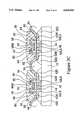
- FIGS. 2A-2Eillustrate a MOSFET and fabrication process steps used to manufacture the MOSFET in substantially pure silicon on sapphire material. Cross sectional views are shown for both N- and P-type transistors. These figures show the device and process through the first level of metallization.
- FIGS. 3A-3Cillustrate an embodiment of the invention comprising adding to the device and process depicted in FIGS. 2, gate sidewall spacers, lightly doped drains (LDD), and self aligned silicide (salicide).
- LDDlightly doped drains
- silicideself aligned silicide
- the present inventionis in the form of an ultrathin intrinsic silicon film on an insulating sapphire substrate wherein the silicon film contains extremely low concentrations of charge states and a process for making same.
- the intrinsic siliconcontains no dopant atoms or electrically active states, either within the silicon film or at the interface between the silicon and the sapphire. While complete elimination of all charge states and dopant atoms is not feasible, trace amounts are acceptable within tolerances determined by the application. For example, if a threshold voltage is to be set to an accuracy of ⁇ Volts, the total charge in the silicon film should be less than about ⁇ /C ox , where C ox is the gate oxide capacitance per unit area. Other tolerances can be determined similarly.
- the total number of fixed charges ⁇ Ni.e., dopant charge plus band gap states plus interface states plus fixed charge in the insulators
- ⁇ V t C ox /qwhere q is the charge on the electron.
- ANshould be less than approximately 2 ⁇ 10 11 cm -2 , which is typical of most current devices.
- certain applicationsmay require tighter threshold voltage control, thereby requiring that the total allowable fixed charge in the silicon film be less than approximately 3 ⁇ 10 11 cm -2 while other applications may tolerate total allowable fixed charge up to as much as 5 ⁇ 10 11 cm -2 .
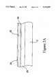
- a 270 nm thick intrinsic silicon film 22is deposited on a sapphire substrate 12 by epitaxial deposition to form a silicon-on-sapphire wafer 11.
- the silicon film 22contains a concentration of twin defects 14 and electrically active states 16.
- the thickness of the silicon film 22is controlled during the epitaxial deposition process using standard processes.
- a 185 keV Beam of Si ions 20is implanted into the silicon film 22 to a dose of approximately 6 ⁇ 10 14 cm -2 , thus creating a subsurface amorphous region 22A and leaving a surface monocrystalline silicon region 22S.
- the energy and dose of the beam of Si ions 20are selected so that the amorphous region 22A extends from an interface 18 formed between the sapphire substrate 12 and the Si film 22 up into the Si film 22 to a thickness which is greater than the desired final thickness of Silicon film.
- the amorphous region 22Ais approximately 200 nm thick.
- the amorphous region 22A in the 270 nm thick intrinsic silicon film 22is created by implantation with the Si ion beam having an energy of 185 keV at a dose of 6 ⁇ 10 14 cm -2 while maintaining the silicon film 22 at a uniform temperature at or below about 0° C. It has been found that this process will uniformly amorphize layer 22A without causing aluminum atoms to be released from the sapphire substrate 12 into the silicon film 22. While others have reported cooling the substrate by placing it on a cooled heat sink during implantation, none have paid particular attention to the temperature of the silicon film 22 during the implantation nor have they adequately addressed the issue of uniform cooling of the silicon film.
- Previous cooling techniquesinclude various techniques for placing the sapphire substrate 12 in contact with a cooled heat sink.
- Contact between the sapphire substrate and the heat sinkwas accomplished in a variety of ways including the use of a thermal paste layer interposed between the sapphire and the heat sink; depositing a layer of indium on the sapphire to provide more uniform contact with the heat sink; polishing the sapphire surface to improve contact with the heat sink; etc.
- these techniquescreated other problems and have been found to be inadequate for forming silicon films free of defects, dopants and charge states.
- a common shortcoming of these techniquesis that it is very difficult to insure that the thermal contact between the sapphire and the heat sink is uniform over the entire sapphire surface.
- Non-uniform contactresults in a nonuniform temperature within the overlying silicon film 22 which creates an amorphous layer 22A which is not uniformly amorphous due to partial self annealing. If the silicon film 22 is held at higher temperatures, the dose and/or energy must be increased to insure amorphization of layer 22A. If the temperature of the silicon film 22 is maintained at too high a temperature or not controlled at all, the ion implantation will cause the substrate temperature to rise, thereby increasing the required dose and/or energy required to amorphize layer 22A to a level where aluminum will outdiffuse from the sapphire 12 into the silicon 22.
- the present inventionovercomes these shortcomings by cooling the sapphire with a flow of cooled gas and by adjusting the gas flow and/or temperature of the gas to insure that the silicon layer 22 is maintained at or below a predetermined temperature.
- the substrate 12is cooled to a temperature which maintains the surface of the silicon film 22 at a temperature preferably lower than about 0° C.
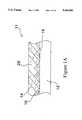
- FIG 1BOne configuration for accomplishing these objectives is illustrated in FIG 1B.
- FIG. 1BShown in FIG. 1B is a configuration for maintaining the silicon film 22 at a uniform temperature at or below about 0° C.
- the SOS wafer 11is positioned on a support structure 17 in a manner which creates a chamber 21 between the sapphire substrate 12 and the support structure 17, for example, by placing an O-ring 19 between the support structure 17 and the SOS wafer 11. Cooled gas is circulated through the chamber 21 to cool the substrate 12. Since the gas has the same thermal contact with all areas of the substrate 12, uniform cooling is assured. Gas enters the chamber 21 through an inlet 23 and exits the chamber through an outlet 25.
- the SOS wafer 11is subjected to a thermal anneal step at approximately 550° C. in an inert atmosphere (e.g. nitrogen) to induce solid phase epitaxial regrowth from the surface of the monocrystalline silicon region 22S downward through the amorphous region 22A to the interface 18.
- an inert atmospheree.g. nitrogen
- the amorphous region 22Ais regrown as a single crystal region 26.
- the direction of the regrowth from the monocrystalline silicon region 22S to the interface 18is depicted by arrows 25 in FIG. 1C.
- the anneal temperatureis increased to approximately 900°-950° C. in an inert atmosphere (e.g.
- a silicon dioxide region 30 having a thickness of approximately 360 nmis then grown in the monocrystalline silicon region 22S by converting the ambient gas in the annealing system from nitrogen to an oxidizing ambient (e.g. steam or oxygen).
- the silicon dioxide region 30is sufficiently thick to consume all the remaining twins 14 and band gap states 16 in the surface region 22S (FIG. 1C) of the silicon film 22.
- the silicon dioxide region 30is sufficiently thick to leave an approximately 110 nm thick region of substantially pure silicon 28 (i.e., containing substantially zero defects and bandgap states) immediately adjacent the sapphire substrate 12.
- the silicon dioxide film 30is removed (etched) to result in an approximately 110 nm thick substantially pure silicon film 28 on the sapphire substrate 12.
- the twins 14 and the states 16 in the upper portion of the silicon filmare removed by forming the silicon dioxide film 30 and etching it away. Removal of the silicon dioxide film 30 may be delayed if it could serve a masking or other purpose.
- the substantially pure silicon film 28 on the sapphire substrate 12is now suited for MOSFET fabrication.
- the above process of the present inventionadvantageously produces the substantially pure ultrathin silicon film 28 and reduces processing costs and complexity by using only one implant cycle and one anneal cycle.
- all of the MOSFET processing stepsare preferably limited to temperatures less than approximately 950° C. in order to maintain the purity of the silicon in channel regions. Additionally, all anneals performed in non-oxidizing conditions are performed at temperatures less than approximately 950° C.
- LOCOSlocal oxidation of silicon
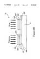
- formation of isolated N-type and P-type regions with the LOCOS processbegins with the deposition of a silicon dioxide layer 36, a silicon nitride layer 32 and a photo-resist layer 33 on top of the silicon layer 28 of the silicon-on-sapphire wafer 11 shown in FIG. 1E.
- individual islands (36p,32p,33p) and (36n,32n,33n) of the silicon dioxide layer 36, silicon nitride layer 32 and photo-resist layer 33are formed on the surface of the Silicon layer 28 as shown in FIG. 2B.
- Standard masking and ion implantation techniquesare used to form a silicon N-type region 22N and a silicon P-type region 22P.
- the silicon N-type region 22Nis formed by ion implantation of the Silicon layer 28 underlying the island (36n,32n,33n) with phosphorus and the silicon P-type region 22P is formed by ion implantation of the Silicon layer 28 underlying the island (36p,32p,33p) with phosphorus.
- the silicon N-type region 22Nis isolated from the silicon P-type region 22P by the growth of a silicon dioxide region 34.
- the silicon dioxide regions 34are grown by introducing the wafer 29 shown in FIG.
- the silicon dioxide isolation regions 34extend down to the sapphire substrate 12. Although the wafer 29 is in an oxidizing ambient, the silicon nitride layer 32 shields the silicon regions 22N and 22P, thereby keeping those regions from oxidizing. After growing the isolation regions 34, the silicon nitride layer 32 and the stress relief oxide layer 36 are stripped away.
- FIG. 2Cshows regions 22N and 22P fully isolated from each other by the silicon dioxide isolation regions 34 for complementary MOS transistors.
- Alternative isolation techniquesmay also be employed.
- the silicon layer 28(FIG. 1E) may be etched into individual islands (sometimes called "mesas").
- the silicon islands 22N and 22Pbecome individual isolated islands or mesas.
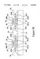
- FIG. 2DA subsequent stage 41 of the MOSFET process is shown in FIG. 2D.
- the N-type and P-type regions 22N and 22Pare further processed to form self aligned sources 42S and 52S, conduction regions 44 and 54, and self aligned drains 42D and 52D, respectively.
- gate insulators 40 and gate conductive layers 48 and 58form a control gate structure.
- the control gate structureis formed by thermal oxidation of the gate insulators 40 followed by deposition and patterning of a chosen gate conductive layer 48 for the P-channel and 58 for the N-channel.
- the gate lengthi.e., the distance separating the source 52S from the drain 52D, be maintained at more than about 5-10 times the thickness of the conduction region.
- a 500 nm gate lengthshould be made in a silicon film thinner than about 100 nm, and preferably closer to 50 nm.
- self aligned sources and drains 42S, 42D, 52S and 52Dare formed by ion implantation or diffusion.
- Doping the source and drain regions of thin silicon filmsis subject to certain limitations. For example, ion implantation doping can amorphize the entire thickness of the source/drain region. An amorphized film will not properly recrystallize from the sapphire substrate and high resistivity may result. Therefore, it is preferable that the source and drain regions be formed by diffusion doping since the sapphire substrate forms a diffusion barrier to the dopant atoms.
- Diffusion doping of the source/drain regionsrepresents an improvement over conventional MOSFET designs using implantation doping in that very thin (i.e., shallow) source/drain regions 42S, 42D, 52S and 52D having low resistivities can be fabricated by means of a single diffusion step.
- Diffusion dopinghas several advantages over ion implantation including: the host silicon is not damaged or transformed into amorphous regions; the process is inherently scalable to the thinnest silicon films; and higher doping concentrations can be achieved.
- Threshold voltage of the control gate structureis initially determined by correctly choosing the gate conductor material according to its so-called metal work function. If necessary, further adjustments to the threshold voltage are made by introducing appropriate dopant atoms into the conduction channel, for example by ion implantation into the conduction regions 44 and 54. In accordance with the present invention, no dopant atoms other than those introduced for threshold adjustment (or to ensure surface channel conduction, see below) are present in the conduction channel regions 44 and 54.
- MOSFET embodiments of the present inventionrepresent an improvement over traditional MOSFET designs wherein substantial concentrations of dopant atoms are typically present for various reasons (e.g., as integral parts of traditional transistors; to provide isolation; as a byproduct of counterdoping; etc.).
- substantial concentrations of dopant atomsare typically present for various reasons (e.g., as integral parts of traditional transistors; to provide isolation; as a byproduct of counterdoping; etc.).
- Gate conductor layers 48 and 58are often multilayer structures.
- the threshold voltageis determined by the characteristics of the primary gate conductor layer, i.e., the layer which is immediately adjacent the gate insulator 40. Conductive layers above the primary gate conductor layer are included for various reasons, especially to reduce series resistance (See FIG. 3 and discussion below for an example). However, such secondary gate conductive layers do not affect the threshold voltage of transistors.
- Each of the gate materials cited belowhas various applications when the material is in contact with the gate insulator 40.
- P + and N + polysilicon gate materialsused in various combinations in N-type MOSFETS and P-type MOSFETS, are useful in designing and fabricating digital and analog circuits, voltage reference circuits and memory type circuits.
- P + polygermaniumis a good choice for high performance digital logic where symmetric threshold voltages for N- and P-type MOSFETs are desired.
- Any conductive material which has a metal work function at the center of silicon's band gapi.e., equal to silicon's electron affinity plus half the band gap or more specifically a metal work function of 4.5-4.7 eV results in symmetric threshold voltages for N- and P-channel MOSFETs.
- Examples of such materialsare tungsten, chrome, indium tin oxide, and titanium nitride, among others.
- the materialmay be different or the same for each transistor type (regions 48 and 58) depending on the desired threshold voltage. Examples of choice of material and resultant threshold voltages are approximately as follows:
- V tn and V tpare the threshold voltages of N- and P-channel MOSFETs, respectively.
- region 48could be P + polysilicon and region 58 could be N + polysilicon (i.e., different materials). If threshold voltages of +1/2 Volt for the N-channel and -1/2 Volt for the P-channel were desired, regions 48 and 58 could be P + polygermanium, tungsten, indium tin oxide or titanium nitride (i.e., the same material). Numerous other material choices, and therefore other choices of threshold voltages, are also available.
- the gate dielectric material 40is grown and the gate conducting materials 48 and 58 are deposited using process conditions which avoid introduction of states or fixed charges into the channel regions 44 and 54. Specifically, processing temperatures and ambients are chosen to avoid generation of interface states or fixed charge in the dielectric. Therefore, as previously discussed, processing temperatures should be kept below approximately 950° C. Also, for P + doped conductors as gate material 48 or 58, processing temperatures, times and ambients should be chosen to avoid diffusion of the dopant atoms from the gate conductors 48 and 58 through the gate dielectric insulator 40 into the silicon films 44 and 54. Diffusion barriers such as silicon nitride as part of the gate dielectric insulator 40 can be used to prevent such dopant migration.
- Surface channel transistor behavioroccurs when conduction occurs in the silicon channels 44 and 54 at the interface between the gate insulator 40 and the silicon films 44 and 54.
- Such a deviceis defined herein as an "intrinsic surface channel MOSFET.” Additional dopant atoms, such as boron, phosphorous or arsenic, may be introduced into the channel regions 44 and 54 to further adjust the threshold voltage of the intrinsic surface channel MOSFET.
- a device constructed in accordance with this inventioncontains only the dopant atoms necessary to induce surface channel conduction and to set threshold voltage. Therefore, none of the other parasitic charge found in traditional MOSFETs are present. The present invention thereby minimizes the dopant charge in regions 44 and 54 and associated adverse effects associated with higher concentrations of dopant charge.
- a maximum amount of dopant chargecan be introduced into channel regions 44 and 54. If the maximum amount is exceeded, the depletion region will not reach the sapphire 12, thus eliminating fully depleted operation.
- the maximum dopant chargeis dependent on the silicon film thickness in the channel regions 44 and 54. For the preferred embodiment, the regions 44 and 54 are approximately 100 nm thick and the maximum dopant density is approximately 1 ⁇ 10 12 cm -2 .
- FIG. 2EA next stage 51 of the MOSFET fabrication process is shown in FIG. 2E.
- insulating layer 62 and metal layer 64are deposited and patterned for interconnecting devices as desired.
- an interlevel insulating layer 62is deposited and patterned, followed by deposition and patterning of a metallic conductor interconnecting layer 64. Additional layers of insulators and metallic conductors may be added as needed (not shown).
- Another advantage of the present inventionis apparent at this point, there are no opportunities for metal to diffuse into the source and drain regions as in many conventional MOSFET fabrication processes.
- an annealing stepis performed.
- This annealing stepserves two primary functions: to remove states and charge which may have been introduced during the previous processing steps and to sinter different metallic layers to form low resistance contacts.
- source and drain junctionsare deep enough to ensure that no metal will diffuse through them and into an underlying silicon substrate, thereby destroying transistors. In the current invention, such a failure mechanism does not exist since only sapphire 12 is found beneath the source and drain regions 42S, 42D, 52S and 52D.
- the current inventionmay also be embodied in a lightly doped drain (LDD) structure or self aligned silicide (salicide).
- LDDlightly doped drain
- silicidesilicide
- FIGS. 3A, 3B and 3CThis embodiment may be implemented after the gate conductors 48 and 58 are patterned as discussed above and shown in FIG. 2D.
- FIG. 3Aafter patterning the gate conductors 48 and 58, self aligned lightly doped drain (LDD) regions 42LD and 52LD are formed by ion implantation or diffusion.
- the LDDreduces electric fields, thereby improving reliability and certain device characteristics such as drain breakdown voltage. However, the LDD also increases series resistance at both the drain and source, thereby decreasing output current.
- a sidewall spacer 60is deposited and etched adjacent to the gate structure comprising the gate insulator 40 and conductor 48, 58.
- final self aligned sources and drains 42S, 42D, 52S and 52Dare formed by ion implantation or diffusion.
- gate conductors 48 and 58such as polysilicon or polygermanium
- the structureis coated with a metallic material and reacted to form metallic compounds 48M and 58M in the upper portion of gate conductors 48 and 58 as well 42M and 52M in source and drain regions 42S, 42D, 52S and 52D.
- silicide regions 42M, 52M, 48M, and 58Mare separated from each other by the sidewall spacers 60.
- the thickness of metallic regions 42M, 48M, 52M and 58Mis controlled by the amount of metallic material which is deposited.
- the salicide optionexists independently of LDD doping level.
- FIG. 3Ca complementary MOS structure is shown with both LDD and salicide options included after metallization as described above for FIG. 2. Many other materials and processing options can be used in addition to or in replacement of those described above. It is to be understood that such choices may be practiced within the scope of this invention.
Landscapes
- Engineering & Computer Science (AREA)
- Microelectronics & Electronic Packaging (AREA)
- Condensed Matter Physics & Semiconductors (AREA)
- General Physics & Mathematics (AREA)
- Manufacturing & Machinery (AREA)
- Computer Hardware Design (AREA)
- Physics & Mathematics (AREA)
- Power Engineering (AREA)
- Chemical & Material Sciences (AREA)
- Crystallography & Structural Chemistry (AREA)
- Materials Engineering (AREA)
- Thin Film Transistor (AREA)
- Metal-Oxide And Bipolar Metal-Oxide Semiconductor Integrated Circuits (AREA)
Abstract
Description
Claims (15)
Priority Applications (23)
| Application Number | Priority Date | Filing Date | Title |
|---|---|---|---|
| US08/090,400US5416043A (en) | 1993-07-12 | 1993-07-12 | Minimum charge FET fabricated on an ultrathin silicon on sapphire wafer |
| US08/218,561US5572040A (en) | 1993-07-12 | 1994-03-25 | High-frequency wireless communication system on a single ultrathin silicon on sapphire chip |
| JP50454195AJP3492372B2 (en) | 1993-07-12 | 1994-06-10 | Semiconductor device and method of manufacturing silicon-on-sapphire wafer having intrinsic silicon layer on sapphire substrate |
| PCT/US1994/006626WO1995002892A1 (en) | 1993-07-12 | 1994-06-10 | High-frequency wireless communication system on a single ultrathin silicon on sapphire chip |
| DE69422714TDE69422714D1 (en) | 1993-07-12 | 1994-06-10 | Method for producing an electronic component on an SOI wafer |
| EP94920168AEP0708980B1 (en) | 1993-07-12 | 1994-06-10 | Method of fabricating an electronic device on a silicon on insulator wafer |
| CA002165334ACA2165334C (en) | 1993-07-12 | 1994-06-10 | High-frequency wireless communication system on a single ultrathin silicon on sapphire chip |
| AT94920168TATE189079T1 (en) | 1993-07-12 | 1994-06-10 | METHOD FOR PRODUCING AN ELECTRONIC COMPONENT ON A SOI WAFER |
| IL11025294AIL110252A0 (en) | 1993-07-12 | 1994-07-08 | Mos device |
| US08/401,521US5973363A (en) | 1993-07-12 | 1995-03-09 | CMOS circuitry with shortened P-channel length on ultrathin silicon on insulator |
| US08/408,750US5863823A (en) | 1993-07-12 | 1995-03-21 | Self-aligned edge control in silicon on insulator |
| US08/408,034US5600169A (en) | 1993-07-12 | 1995-03-21 | Minimum charge FET fabricated on an ultrathin silicon on sapphire wafer |
| US08/437,608US5492857A (en) | 1993-07-12 | 1995-05-09 | High-frequency wireless communication system on a single ultrathin silicon on sapphire chip |
| US08/445,144US5596205A (en) | 1993-07-12 | 1995-05-19 | High-frequency wireless communication system on a single ultrathin silicon on sapphire chip |
| US08/444,992US5663570A (en) | 1993-07-12 | 1995-05-19 | High-frequency wireless communication system on a single ultrathin silicon on sapphire chip |
| US08/565,682US5861336A (en) | 1993-07-12 | 1995-11-30 | High-frequency wireless communication system on a single ultrathin silicon on sapphire chip |
| US08/733,320US5883396A (en) | 1993-07-12 | 1996-10-17 | High-frequency wireless communication system on a single ultrathin silicon on sapphire chip |
| US08/571,661US5864162A (en) | 1993-07-12 | 1996-12-13 | Apparatus and method of making a self-aligned integrated resistor load on ultrathin silicon on sapphire |
| US08/778,669US5895957A (en) | 1993-07-12 | 1997-01-03 | Minimum charge FET fabricated on an ultrathin silicon on sapphire wafer |
| US08/862,575US5973382A (en) | 1993-07-12 | 1997-05-23 | Capacitor on ultrathin semiconductor on insulator |
| US08/914,474US5930638A (en) | 1993-07-12 | 1997-08-19 | Method of making a low parasitic resistor on ultrathin silicon on insulator |
| US09/144,841US6090648A (en) | 1993-07-12 | 1998-08-31 | Method of making a self-aligned integrated resistor load on ultrathin silicon on sapphire |
| US09/179,258US6057555A (en) | 1993-07-12 | 1998-10-26 | High-frequency wireless communication system on a single ultrathin silicon on sapphire chip |
Applications Claiming Priority (1)
| Application Number | Priority Date | Filing Date | Title |
|---|---|---|---|
| US08/090,400US5416043A (en) | 1993-07-12 | 1993-07-12 | Minimum charge FET fabricated on an ultrathin silicon on sapphire wafer |
Related Child Applications (4)
| Application Number | Title | Priority Date | Filing Date |
|---|---|---|---|
| US08/218,561Continuation-In-PartUS5572040A (en) | 1993-07-12 | 1994-03-25 | High-frequency wireless communication system on a single ultrathin silicon on sapphire chip |
| US38967195AContinuation-In-Part | 1993-07-12 | 1995-02-16 | |
| US08/408,034DivisionUS5600169A (en) | 1993-07-12 | 1995-03-21 | Minimum charge FET fabricated on an ultrathin silicon on sapphire wafer |
| US08/408,750Continuation-In-PartUS5863823A (en) | 1993-07-12 | 1995-03-21 | Self-aligned edge control in silicon on insulator |
Publications (1)
| Publication Number | Publication Date |
|---|---|
| US5416043Atrue US5416043A (en) | 1995-05-16 |
Family
ID=22222617
Family Applications (3)
| Application Number | Title | Priority Date | Filing Date |
|---|---|---|---|
| US08/090,400Expired - LifetimeUS5416043A (en) | 1993-07-12 | 1993-07-12 | Minimum charge FET fabricated on an ultrathin silicon on sapphire wafer |
| US08/408,034Expired - LifetimeUS5600169A (en) | 1993-07-12 | 1995-03-21 | Minimum charge FET fabricated on an ultrathin silicon on sapphire wafer |
| US08/778,669Expired - LifetimeUS5895957A (en) | 1993-07-12 | 1997-01-03 | Minimum charge FET fabricated on an ultrathin silicon on sapphire wafer |
Family Applications After (2)
| Application Number | Title | Priority Date | Filing Date |
|---|---|---|---|
| US08/408,034Expired - LifetimeUS5600169A (en) | 1993-07-12 | 1995-03-21 | Minimum charge FET fabricated on an ultrathin silicon on sapphire wafer |
| US08/778,669Expired - LifetimeUS5895957A (en) | 1993-07-12 | 1997-01-03 | Minimum charge FET fabricated on an ultrathin silicon on sapphire wafer |
Country Status (1)
| Country | Link |
|---|---|
| US (3) | US5416043A (en) |
Cited By (76)
| Publication number | Priority date | Publication date | Assignee | Title |
|---|---|---|---|---|
| EP0889505A1 (en)* | 1997-07-03 | 1999-01-07 | STMicroelectronics S.r.l. | Process for cutting trenches in a single crystal substrate |
| US5861336A (en)* | 1993-07-12 | 1999-01-19 | Peregrine Semiconductor Corporation | High-frequency wireless communication system on a single ultrathin silicon on sapphire chip |
| US5863823A (en)* | 1993-07-12 | 1999-01-26 | Peregrine Semiconductor Corporation | Self-aligned edge control in silicon on insulator |
| US5864162A (en)* | 1993-07-12 | 1999-01-26 | Peregrine Seimconductor Corporation | Apparatus and method of making a self-aligned integrated resistor load on ultrathin silicon on sapphire |
| US5893729A (en)* | 1995-06-28 | 1999-04-13 | Honeywell Inc. | Method of making SOI circuit for higher temperature and higher voltage applications |
| US5930638A (en)* | 1993-07-12 | 1999-07-27 | Peregrine Semiconductor Corp. | Method of making a low parasitic resistor on ultrathin silicon on insulator |
| US5973363A (en)* | 1993-07-12 | 1999-10-26 | Peregrine Semiconductor Corp. | CMOS circuitry with shortened P-channel length on ultrathin silicon on insulator |
| US5973382A (en)* | 1993-07-12 | 1999-10-26 | Peregrine Semiconductor Corporation | Capacitor on ultrathin semiconductor on insulator |
| US6441399B1 (en)* | 1994-04-22 | 2002-08-27 | Semiconductor Energy Laboratory Co., Ltd. | Semiconductor integrated system |
| WO2002075785A3 (en)* | 2001-03-16 | 2003-02-27 | Peregrine Semiconductor Corp | Coupled optical and optoelectronic devices, and method of making the same |
| US6528387B1 (en) | 1997-06-19 | 2003-03-04 | Asahi Kasei Kabushiki Kaisha | SOI substrate and process for preparing the same, and semiconductor device and process for preparing the same |
| US20030076765A1 (en)* | 2001-10-18 | 2003-04-24 | Ayres Mark R. | Holographic recording using contact prisms |
| US6583445B1 (en) | 2000-06-16 | 2003-06-24 | Peregrine Semiconductor Corporation | Integrated electronic-optoelectronic devices and method of making the same |
| US6653885B2 (en) | 2001-05-03 | 2003-11-25 | Peregrine Semiconductor Corporation | On-chip integrated mixer with balun circuit and method of making the same |
| US20030219750A1 (en)* | 1999-03-30 | 2003-11-27 | Genset, S.A. | Schizophrenia associated genes, proteins and biallelic markers |
| US6667506B1 (en) | 1999-04-06 | 2003-12-23 | Peregrine Semiconductor Corporation | Variable capacitor with programmability |
| US6690056B1 (en) | 1999-04-06 | 2004-02-10 | Peregrine Semiconductor Corporation | EEPROM cell on SOI |
| US6747627B1 (en) | 1994-04-22 | 2004-06-08 | Semiconductor Energy Laboratory Co., Ltd. | Redundancy shift register circuit for driver circuit in active matrix type liquid crystal display device |
| US6804502B2 (en) | 2001-10-10 | 2004-10-12 | Peregrine Semiconductor Corporation | Switch circuit and method of switching radio frequency signals |
| US20050104176A1 (en)* | 2003-11-18 | 2005-05-19 | Halliburton Energy Services, Inc. | High temperature electronic devices |
| US20050103980A1 (en)* | 2003-11-18 | 2005-05-19 | Halliburton Energy Services, Inc. | High temperature imaging device |
| US20050104104A1 (en)* | 2003-11-18 | 2005-05-19 | Halliburton Energy Services, Inc. | High temperature memory device |
| US20050179483A1 (en)* | 2003-11-18 | 2005-08-18 | Hutchens Chriswell G. | High-voltage transistors on insulator substrates |
| EP1120818A4 (en)* | 1998-09-25 | 2005-09-14 | Asahi Chemical Ind | Semiconductor substrate and its production method, semiconductor device comprising the same and its production method |
| US20060194567A1 (en)* | 2001-10-10 | 2006-08-31 | Kelly Dylan J | Symmetrically and asymmetrically stacked transistor grouping RF switch |
| US20060199563A1 (en)* | 2005-02-09 | 2006-09-07 | Kelly Dylan J | Unpowered switch and bleeder circuit |
| US20060226486A1 (en)* | 2005-04-06 | 2006-10-12 | Masahiko Kasuga | Semiconductor device |
| US20070018277A1 (en)* | 2005-07-05 | 2007-01-25 | Oki Electric Industry Co., Ltd. | Field effect transistor and semiconductor device |
| US20070018247A1 (en)* | 2005-07-11 | 2007-01-25 | Brindle Christopher N | Method and apparatus for use in improving linearity of MOSFET's using an accumulated charge sink |
| US7192840B2 (en)* | 2002-10-30 | 2007-03-20 | Oki Electric Industry Co., Ltd. | Semiconductor device fabrication method using oxygen ion implantation |
| US20070069291A1 (en)* | 2005-07-11 | 2007-03-29 | Stuber Michael A | Method and apparatus improving gate oxide reliability by controlling accumulated charge |
| US20090130415A1 (en)* | 2007-11-21 | 2009-05-21 | Saint-Gobain Ceramics & Plastics, Inc. | R-Plane Sapphire Method and Apparatus |
| US7613442B1 (en) | 2001-10-10 | 2009-11-03 | Peregrine Semiconductor Corporation | Switch circuit and method of switching radio frequency signals |
| RU2390874C1 (en)* | 2009-01-30 | 2010-05-27 | Общество с ограниченной ответственностью Научно-производственная фирма "Топаз-К" | Method for obtaining heteroepitaxial silicon-on-sapphire structures |
| US20100282160A1 (en)* | 2004-04-08 | 2010-11-11 | Saint-Gobain Ceramics & Plastics, Inc. | Single crystals and methods for fabricating same |
| US20110001542A1 (en)* | 2008-02-28 | 2011-01-06 | Tero Tapio Ranta | Devices and methods for improving voltage handling and/or bi-directionality of stacks of elements when connected between terminals |
| RU2427941C1 (en)* | 2010-06-01 | 2011-08-27 | Федеральное государственное бюджетное учреждение "Национальный исследовательский центр "Курчатовский институт" | Method of producing super-thin silicon films on sapphire |
| US8131251B2 (en) | 2004-06-23 | 2012-03-06 | Peregrine Semiconductor Corporation | Integrated RF front end with stacked transistor switch |
| WO2012054642A1 (en) | 2010-10-20 | 2012-04-26 | Peregrine Semiconductor Corporation | Method and apparatus for use in improving linearity of mosfets using an accumulated charge sink - harmonic wrinkle reduction |
| US8536636B2 (en) | 2007-04-26 | 2013-09-17 | Peregrine Semiconductor Corporation | Tuning capacitance to enhance FET stack voltage withstand |
| US8723260B1 (en) | 2009-03-12 | 2014-05-13 | Rf Micro Devices, Inc. | Semiconductor radio frequency switch with body contact |
| US8729952B2 (en) | 2012-08-16 | 2014-05-20 | Triquint Semiconductor, Inc. | Switching device with non-negative biasing |
| US8742502B2 (en) | 2005-07-11 | 2014-06-03 | Peregrine Semiconductor Corporation | Method and apparatus for use in improving linearity of MOSFETs using an accumulated charge sink-harmonic wrinkle reduction |
| US8791529B2 (en) | 2010-02-05 | 2014-07-29 | Semiconductor Energy Laboratory Co., Ltd. | Semiconductor device including gate and conductor electrodes |
| US8829967B2 (en) | 2012-06-27 | 2014-09-09 | Triquint Semiconductor, Inc. | Body-contacted partially depleted silicon on insulator transistor |
| US8847672B2 (en) | 2013-01-15 | 2014-09-30 | Triquint Semiconductor, Inc. | Switching device with resistive divider |
| US8923782B1 (en) | 2013-02-20 | 2014-12-30 | Triquint Semiconductor, Inc. | Switching device with diode-biased field-effect transistor (FET) |
| US8977217B1 (en) | 2013-02-20 | 2015-03-10 | Triquint Semiconductor, Inc. | Switching device with negative bias circuit |
| KR20150037896A (en)* | 2012-07-25 | 2015-04-08 | 신에쓰 가가꾸 고교 가부시끼가이샤 | Method for producing sos substrates, and sos substrate |
| US9203396B1 (en) | 2013-02-22 | 2015-12-01 | Triquint Semiconductor, Inc. | Radio frequency switch device with source-follower |
| US9214932B2 (en) | 2013-02-11 | 2015-12-15 | Triquint Semiconductor, Inc. | Body-biased switching device |
| US9379698B2 (en) | 2014-02-04 | 2016-06-28 | Triquint Semiconductor, Inc. | Field effect transistor switching circuit |
| US9397656B2 (en) | 2005-07-11 | 2016-07-19 | Peregrine Semiconductor Corporation | Circuit and method for controlling charge injection in radio frequency switches |
| US9406695B2 (en) | 2013-11-20 | 2016-08-02 | Peregrine Semiconductor Corporation | Circuit and method for improving ESD tolerance and switching speed |
| US9419565B2 (en) | 2013-03-14 | 2016-08-16 | Peregrine Semiconductor Corporation | Hot carrier injection compensation |
| US9484897B2 (en) | 2015-03-18 | 2016-11-01 | Peregrine Semiconductor Corporation | Level shifter |
| US9590674B2 (en) | 2012-12-14 | 2017-03-07 | Peregrine Semiconductor Corporation | Semiconductor devices with switchable ground-body connection |
| US9705482B1 (en) | 2016-06-24 | 2017-07-11 | Peregrine Semiconductor Corporation | High voltage input buffer |
| US9831857B2 (en) | 2015-03-11 | 2017-11-28 | Peregrine Semiconductor Corporation | Power splitter with programmable output phase shift |
| US9847348B1 (en) | 2016-12-20 | 2017-12-19 | Peregrine Semiconductor Corporation | Systems, methods and apparatus for enabling high voltage circuits |
| US9912327B2 (en) | 2015-03-18 | 2018-03-06 | Peregrine Semiconductor Corporation | Dead time control circuit for a level shifter |
| US9948281B2 (en) | 2016-09-02 | 2018-04-17 | Peregrine Semiconductor Corporation | Positive logic digitally tunable capacitor |
| US10116297B1 (en) | 2017-06-19 | 2018-10-30 | Psemi Corporation | DC-coupled high-voltage level shifter |
| US10236872B1 (en) | 2018-03-28 | 2019-03-19 | Psemi Corporation | AC coupling modules for bias ladders |
| US10348293B2 (en) | 2017-06-19 | 2019-07-09 | Psemi Corporation | Timing controller for dead-time control |
| US10505530B2 (en) | 2018-03-28 | 2019-12-10 | Psemi Corporation | Positive logic switch with selectable DC blocking circuit |
| US10672726B2 (en) | 2017-05-19 | 2020-06-02 | Psemi Corporation | Transient stabilized SOI FETs |
| RU2735129C1 (en)* | 2020-03-14 | 2020-10-28 | Акционерное общество "Научно-исследовательский институт материаловедения им. А. Ю. Малинина" (АО "НИИ МВ") | Apparatus and method for cooling epitaxial structures |
| US10886911B2 (en) | 2018-03-28 | 2021-01-05 | Psemi Corporation | Stacked FET switch bias ladders |
| US10971359B2 (en) | 2017-05-19 | 2021-04-06 | Psemi Corporation | Managed substrate effects for stabilized SOI FETs |
| US11011633B2 (en) | 2005-07-11 | 2021-05-18 | Psemi Corporation | Method and apparatus for use in improving linearity of MOSFETs using an accumulated charge sink-harmonic wrinkle reduction |
| US11047650B2 (en) | 2017-09-29 | 2021-06-29 | Saint-Gobain Ceramics & Plastics, Inc. | Transparent composite having a laminated structure |
| USRE48965E1 (en) | 2005-07-11 | 2022-03-08 | Psemi Corporation | Method and apparatus improving gate oxide reliability by controlling accumulated charge |
| US11355499B2 (en) | 2016-11-17 | 2022-06-07 | Taiwan Semiconductor Manufacturing Co., Ltd. | Static random access memory cell |
| US11476849B2 (en) | 2020-01-06 | 2022-10-18 | Psemi Corporation | High power positive logic switch |
| WO2023042568A1 (en) | 2021-09-17 | 2023-03-23 | 株式会社タムラ製作所 | P-n junction diode |
Families Citing this family (44)
| Publication number | Priority date | Publication date | Assignee | Title |
|---|---|---|---|---|
| US5895933A (en)* | 1993-06-25 | 1999-04-20 | Semiconductor Energy Laboratory Co., Ltd. | Semiconductor device and method for its preparation |
| US6730549B1 (en) | 1993-06-25 | 2004-05-04 | Semiconductor Energy Laboratory Co., Ltd. | Semiconductor device and method for its preparation |
| US6312968B1 (en) | 1993-06-30 | 2001-11-06 | The United States Of America As Represented By The Secretary Of The Navy | Method for fabricating an electrically addressable silicon-on-sapphire light valve |
| US6190933B1 (en) | 1993-06-30 | 2001-02-20 | The United States Of America As Represented By The Secretary Of The Navy | Ultra-high resolution liquid crystal display on silicon-on-sapphire |
| US5942768A (en)* | 1994-10-07 | 1999-08-24 | Semionductor Energy Laboratory Co., Ltd. | Semiconductor device having improved crystal orientation |
| KR100331844B1 (en)* | 1998-02-12 | 2002-05-10 | 박종섭 | Complementary metal oxide semiconductor device |
| US6027961A (en)* | 1998-06-30 | 2000-02-22 | Motorola, Inc. | CMOS semiconductor devices and method of formation |
| TW484117B (en) | 1999-11-08 | 2002-04-21 | Semiconductor Energy Lab | Electronic device |
| US6992652B2 (en)* | 2000-08-08 | 2006-01-31 | Semiconductor Energy Laboratory Co., Ltd. | Liquid crystal display device and driving method thereof |
| TW522374B (en)* | 2000-08-08 | 2003-03-01 | Semiconductor Energy Lab | Electro-optical device and driving method of the same |
| US7180496B2 (en)* | 2000-08-18 | 2007-02-20 | Semiconductor Energy Laboratory Co., Ltd. | Liquid crystal display device and method of driving the same |
| US6987496B2 (en)* | 2000-08-18 | 2006-01-17 | Semiconductor Energy Laboratory Co., Ltd. | Electronic device and method of driving the same |
| TW518552B (en) | 2000-08-18 | 2003-01-21 | Semiconductor Energy Lab | Liquid crystal display device, method of driving the same, and method of driving a portable information device having the liquid crystal display device |
| TW514854B (en)* | 2000-08-23 | 2002-12-21 | Semiconductor Energy Lab | Portable information apparatus and method of driving the same |
| US7642566B2 (en)* | 2006-06-12 | 2010-01-05 | Dsm Solutions, Inc. | Scalable process and structure of JFET for small and decreasing line widths |
| JP4014831B2 (en)* | 2000-09-04 | 2007-11-28 | 株式会社半導体エネルギー研究所 | EL display device and driving method thereof |
| KR100823047B1 (en) | 2000-10-02 | 2008-04-18 | 가부시키가이샤 한도오따이 에네루기 켄큐쇼 | Self-luminescent device and driving method thereof |
| US7184014B2 (en)* | 2000-10-05 | 2007-02-27 | Semiconductor Energy Laboratory Co., Ltd. | Liquid crystal display device |
| US6448590B1 (en) | 2000-10-24 | 2002-09-10 | International Business Machines Corporation | Multiple threshold voltage FET using multiple work-function gate materials |
| US6747623B2 (en)* | 2001-02-09 | 2004-06-08 | Semiconductor Energy Laboratory Co., Ltd. | Liquid crystal display device and method of driving the same |
| TW480735B (en)* | 2001-04-24 | 2002-03-21 | United Microelectronics Corp | Structure and manufacturing method of polysilicon thin film transistor |
| US6720830B2 (en)* | 2001-06-11 | 2004-04-13 | Johns Hopkins University | Low-power, differential optical receiver in silicon on insulator |
| JP2003114646A (en)* | 2001-08-03 | 2003-04-18 | Semiconductor Energy Lab Co Ltd | Display device and its driving method |
| TWI273539B (en) | 2001-11-29 | 2007-02-11 | Semiconductor Energy Lab | Display device and display system using the same |
| JP3913534B2 (en)* | 2001-11-30 | 2007-05-09 | 株式会社半導体エネルギー研究所 | Display device and display system using the same |
| JP4067878B2 (en)* | 2002-06-06 | 2008-03-26 | 株式会社半導体エネルギー研究所 | Light emitting device and electric appliance using the same |
| US6982727B2 (en)* | 2002-07-23 | 2006-01-03 | Broadcom Corporation | System and method for providing graphics using graphical engine |
| KR100581886B1 (en)* | 2003-11-21 | 2006-05-22 | 삼성에스디아이 주식회사 | Thin film transistor with threshold voltage and flat panel display device having the same |
| JP2005275315A (en)* | 2004-03-26 | 2005-10-06 | Semiconductor Energy Lab Co Ltd | Display device, driving method therefor, and electronic equipment using the same |
| US7502040B2 (en)* | 2004-12-06 | 2009-03-10 | Semiconductor Energy Laboratory Co., Ltd. | Display device, driving method thereof and electronic appliance |
| US20060139265A1 (en)* | 2004-12-28 | 2006-06-29 | Semiconductor Energy Laboratory Co., Ltd. | Driving method of display device |
| US20060158399A1 (en) | 2005-01-14 | 2006-07-20 | Semiconductor Energy Laboratory Co., Ltd. | Driving method of display device |
| US7719526B2 (en) | 2005-04-14 | 2010-05-18 | Semiconductor Energy Laboratory Co., Ltd. | Display device, and driving method and electronic apparatus of the display device |
| US8633919B2 (en)* | 2005-04-14 | 2014-01-21 | Semiconductor Energy Laboratory Co., Ltd. | Display device, driving method of the display device, and electronic device |
| EP2264690A1 (en) | 2005-05-02 | 2010-12-22 | Semiconductor Energy Laboratory Co, Ltd. | Display device and gray scale driving method with subframes thereof |
| US20070131985A1 (en)* | 2005-11-29 | 2007-06-14 | Kazunori Fujita | Semiconductor device and method for manufacturing the same |
| KR101404582B1 (en)* | 2006-01-20 | 2014-06-09 | 가부시키가이샤 한도오따이 에네루기 켄큐쇼 | Method of driving display device |
| US7977736B2 (en)* | 2006-02-23 | 2011-07-12 | Samsung Electronics Co., Ltd. | Vertical channel transistors and memory devices including vertical channel transistors |
| WO2009072983A1 (en)* | 2007-12-07 | 2009-06-11 | Agency For Science, Technology And Research | Memory cell and methods of manufacturing thereof |
| WO2009072984A1 (en)* | 2007-12-07 | 2009-06-11 | Agency For Science, Technology And Research | A silicon-germanium nanowire structure and a method of forming the same |
| US8962376B2 (en)* | 2009-04-21 | 2015-02-24 | The Silanna Group Pty Ltd | Optoelectronic device with lateral pin or pin junction |
| WO2010141994A1 (en)* | 2009-06-12 | 2010-12-16 | The Silanna Group Pty Ltd | Process for producing a semiconductor-on-sapphire article |
| US9034717B2 (en)* | 2013-10-16 | 2015-05-19 | Taiwan Semiconductor Manufacturing Company Limited | Semiconductor-on-insulator structure and method of fabricating the same |
| US12205936B2 (en) | 2021-09-16 | 2025-01-21 | International Business Machines Corporation | Silicon on sapphire substrate for edge computer |
Citations (22)
| Publication number | Priority date | Publication date | Assignee | Title |
|---|---|---|---|---|
| US4177084A (en)* | 1978-06-09 | 1979-12-04 | Hewlett-Packard Company | Method for producing a low defect layer of silicon-on-sapphire wafer |
| US4198649A (en)* | 1976-09-03 | 1980-04-15 | Fairchild Camera And Instrument Corporation | Memory cell structure utilizing conductive buried regions |
| US4385937A (en)* | 1980-05-20 | 1983-05-31 | Tokyo Shibaura Denki Kabushiki Kaisha | Regrowing selectively formed ion amorphosized regions by thermal gradient |
| US4418470A (en)* | 1981-10-21 | 1983-12-06 | General Electric Company | Method for fabricating silicon-on-sapphire monolithic microwave integrated circuits |
| US4425700A (en)* | 1980-08-13 | 1984-01-17 | Fujitsu Limited | Semiconductor device and method for manufacturing the same |
| US4463492A (en)* | 1981-09-30 | 1984-08-07 | Tokyo Shibaura Denki Kabushiki Kaisha | Method of forming a semiconductor device on insulating substrate by selective amorphosization followed by simultaneous activation and reconversion to single crystal state |
| US4509990A (en)* | 1982-11-15 | 1985-04-09 | Hughes Aircraft Company | Solid phase epitaxy and regrowth process with controlled defect density profiling for heteroepitaxial semiconductor on insulator composite substrates |
| US4523963A (en)* | 1983-03-02 | 1985-06-18 | Tokyo Shibaura Denki Kabushiki Kaisha | Method of fabricating MOS device on a SOS wafer by stabilizing interface region with silicon and oxygen implant |
| US4588447A (en)* | 1984-06-25 | 1986-05-13 | Rockwell International Corporation | Method of eliminating p-type electrical activity and increasing channel mobility of Si-implanted and recrystallized SOS films |
| JPS61103530A (en)* | 1984-10-25 | 1986-05-22 | Ulvac Corp | Cooling mechanism of substrate in vacuum treatment device |
| US4607176A (en)* | 1984-08-22 | 1986-08-19 | The United States Of America As Represented By The Secretary Of The Air Force | Tally cell circuit |
| US4615762A (en)* | 1985-04-30 | 1986-10-07 | Rca Corporation | Method for thinning silicon |
| US4617066A (en)* | 1984-11-26 | 1986-10-14 | Hughes Aircraft Company | Process of making semiconductors having shallow, hyperabrupt doped regions by implantation and two step annealing |
| US4659392A (en)* | 1985-03-21 | 1987-04-21 | Hughes Aircraft Company | Selective area double epitaxial process for fabricating silicon-on-insulator structures for use with MOS devices and integrated circuits |
| JPS62176145A (en)* | 1986-01-29 | 1987-08-01 | Sharp Corp | Manufacture of semiconductor substrate |
| US4766482A (en)* | 1986-12-09 | 1988-08-23 | General Electric Company | Semiconductor device and method of making the same |
| US4775641A (en)* | 1986-09-25 | 1988-10-04 | General Electric Company | Method of making silicon-on-sapphire semiconductor devices |
| US4843448A (en)* | 1988-04-18 | 1989-06-27 | The United States Of America As Represented By The Secretary Of The Navy | Thin-film integrated injection logic |
| WO1989007367A2 (en)* | 1988-02-08 | 1989-08-10 | Hughes Aircraft Company | Analog-to-digital converter made with focused ion beam technology |
| US5027171A (en)* | 1989-08-28 | 1991-06-25 | The United States Of America As Represented By The Secretary Of The Navy | Dual polarity floating gate MOS analog memory device |
| JPH04122020A (en)* | 1990-09-12 | 1992-04-22 | Fujitsu Ltd | Vapor phase epitaxy method |
| US5300443A (en)* | 1993-06-30 | 1994-04-05 | The United States Of America As Represented By The Secretary Of The Navy | Method for fabricating complementary enhancement and depletion mode field effect transistors on a single substrate |
Family Cites Families (5)
| Publication number | Priority date | Publication date | Assignee | Title |
|---|---|---|---|---|
| US3562608A (en)* | 1969-03-24 | 1971-02-09 | Westinghouse Electric Corp | Variable integrated coupler |
| US3798508A (en)* | 1969-09-18 | 1974-03-19 | Matsushita Electric Industrial Co Ltd | Variable capacitance device |
| US5229644A (en)* | 1987-09-09 | 1993-07-20 | Casio Computer Co., Ltd. | Thin film transistor having a transparent electrode and substrate |
| US5141882A (en)* | 1989-04-05 | 1992-08-25 | Mitsubishi Denki Kabushiki Kaisha | Semiconductor field effect device having channel stop and channel region formed in a well and manufacturing method therefor |
| US5102809A (en)* | 1990-10-11 | 1992-04-07 | Texas Instruments Incorporated | SOI BICMOS process |
- 1993
- 1993-07-12USUS08/090,400patent/US5416043A/ennot_activeExpired - Lifetime
- 1995
- 1995-03-21USUS08/408,034patent/US5600169A/ennot_activeExpired - Lifetime
- 1997
- 1997-01-03USUS08/778,669patent/US5895957A/ennot_activeExpired - Lifetime
Patent Citations (22)
| Publication number | Priority date | Publication date | Assignee | Title |
|---|---|---|---|---|
| US4198649A (en)* | 1976-09-03 | 1980-04-15 | Fairchild Camera And Instrument Corporation | Memory cell structure utilizing conductive buried regions |
| US4177084A (en)* | 1978-06-09 | 1979-12-04 | Hewlett-Packard Company | Method for producing a low defect layer of silicon-on-sapphire wafer |
| US4385937A (en)* | 1980-05-20 | 1983-05-31 | Tokyo Shibaura Denki Kabushiki Kaisha | Regrowing selectively formed ion amorphosized regions by thermal gradient |
| US4425700A (en)* | 1980-08-13 | 1984-01-17 | Fujitsu Limited | Semiconductor device and method for manufacturing the same |
| US4463492A (en)* | 1981-09-30 | 1984-08-07 | Tokyo Shibaura Denki Kabushiki Kaisha | Method of forming a semiconductor device on insulating substrate by selective amorphosization followed by simultaneous activation and reconversion to single crystal state |
| US4418470A (en)* | 1981-10-21 | 1983-12-06 | General Electric Company | Method for fabricating silicon-on-sapphire monolithic microwave integrated circuits |
| US4509990A (en)* | 1982-11-15 | 1985-04-09 | Hughes Aircraft Company | Solid phase epitaxy and regrowth process with controlled defect density profiling for heteroepitaxial semiconductor on insulator composite substrates |
| US4523963A (en)* | 1983-03-02 | 1985-06-18 | Tokyo Shibaura Denki Kabushiki Kaisha | Method of fabricating MOS device on a SOS wafer by stabilizing interface region with silicon and oxygen implant |
| US4588447A (en)* | 1984-06-25 | 1986-05-13 | Rockwell International Corporation | Method of eliminating p-type electrical activity and increasing channel mobility of Si-implanted and recrystallized SOS films |
| US4607176A (en)* | 1984-08-22 | 1986-08-19 | The United States Of America As Represented By The Secretary Of The Air Force | Tally cell circuit |
| JPS61103530A (en)* | 1984-10-25 | 1986-05-22 | Ulvac Corp | Cooling mechanism of substrate in vacuum treatment device |
| US4617066A (en)* | 1984-11-26 | 1986-10-14 | Hughes Aircraft Company | Process of making semiconductors having shallow, hyperabrupt doped regions by implantation and two step annealing |
| US4659392A (en)* | 1985-03-21 | 1987-04-21 | Hughes Aircraft Company | Selective area double epitaxial process for fabricating silicon-on-insulator structures for use with MOS devices and integrated circuits |
| US4615762A (en)* | 1985-04-30 | 1986-10-07 | Rca Corporation | Method for thinning silicon |
| JPS62176145A (en)* | 1986-01-29 | 1987-08-01 | Sharp Corp | Manufacture of semiconductor substrate |
| US4775641A (en)* | 1986-09-25 | 1988-10-04 | General Electric Company | Method of making silicon-on-sapphire semiconductor devices |
| US4766482A (en)* | 1986-12-09 | 1988-08-23 | General Electric Company | Semiconductor device and method of making the same |
| WO1989007367A2 (en)* | 1988-02-08 | 1989-08-10 | Hughes Aircraft Company | Analog-to-digital converter made with focused ion beam technology |
| US4843448A (en)* | 1988-04-18 | 1989-06-27 | The United States Of America As Represented By The Secretary Of The Navy | Thin-film integrated injection logic |
| US5027171A (en)* | 1989-08-28 | 1991-06-25 | The United States Of America As Represented By The Secretary Of The Navy | Dual polarity floating gate MOS analog memory device |
| JPH04122020A (en)* | 1990-09-12 | 1992-04-22 | Fujitsu Ltd | Vapor phase epitaxy method |
| US5300443A (en)* | 1993-06-30 | 1994-04-05 | The United States Of America As Represented By The Secretary Of The Navy | Method for fabricating complementary enhancement and depletion mode field effect transistors on a single substrate |
Non-Patent Citations (28)
| Title |
|---|
| Adele E. Schmitz et al., "A Deep-Submicrometer Microwave/Digital CMOS/SOS Technology", IEE Electron Device Letters, vol. 12, No. 1, pp. 16-17, Jan. 1991. |
| Adele E. Schmitz et al., A Deep Submicrometer Microwave/Digital CMOS/SOS Technology , IEE Electron Device Letters, vol. 12, No. 1, pp. 16 17, Jan. 1991.* |
| G. A. Garcia et al., "High-Quality CMOS on Thin (100 nm) Silicon on Sapphire", IEEE Electron Device Letters, vol. 9, No. 1, pp. 32-34, Jan. 1988. |
| G. A. Garcia et al., High Quality CMOS on Thin (100 nm) Silicon on Sapphire , IEEE Electron Device Letters, vol. 9, No. 1, pp. 32 34, Jan. 1988.* |
| Golecki et al., "Recrystallization of Silicon-on-sapphire by CW Ar laser irradiaton: Comparison between the solid and the liquid-phase regimes"; Appl. Phys. Lett. 37(10), 1980, pp. 919-921. |
| Golecki et al., Recrystallization of Silicon on sapphire by CW Ar laser irradiaton: Comparison between the solid and the liquid phase regimes ; Appl. Phys. Lett. 37(10), 1980, pp. 919 921.* |
| Golecki et al.; "Improvement of crystalline quality of epitaxial silicon-on-sapphire by ion-implantation and furnace regrowth"; Solid State Electronics vol. 23, 1980, pp. 803-806. |
| Golecki et al.; Improvement of crystalline quality of epitaxial silicon on sapphire by ion implantation and furnace regrowth ; Solid State Electronics vol. 23, 1980, pp. 803 806.* |
| Inoue et al., "Crystalline disorder reduction and defect-type change in silicon-on-sapphire films by silicon implantation and subsequent thermal annealing"; Appl. Phys. Lett. 36(1), 1980, pp. 64-66. |
| Inoue et al., Crystalline disorder reduction and defect type change in silicon on sapphire films by silicon implantation and subsequent thermal annealing ; Appl. Phys. Lett. 36(1), 1980, pp. 64 66.* |
| Lau et al. "Improvement of crystalline quality of epitaxial Si layers by ion implantation techniques"; Appl. Phys. Lett. 34(1), 1979, pp. 76-78. |
| Lau et al. Improvement of crystalline quality of epitaxial Si layers by ion implantation techniques ; Appl. Phys. Lett. 34(1), 1979, pp. 76 78.* |
| Linnros et al. "Ion-beam induced epitaxial regrowth of amorphous layers in silicon on sapphire"; Physical Review B, vol. 30, No. 7, 1984, pp. 3629-3638. |
| Linnros et al. Ion beam induced epitaxial regrowth of amorphous layers in silicon on sapphire ; Physical Review B, vol. 30, No. 7, 1984, pp. 3629 3638.* |
| Nobuo Sasaki et al., "A CMOS/SOS Synchronous Static RAM Fabricated with an Advanced SOS Technology", Japanese Journal of Applied Physics, Supplement 18-1, vol. 18, pp. 57-62, 1979. |
| Nobuo Sasaki et al., A CMOS/SOS Synchronous Static RAM Fabricated with an Advanced SOS Technology , Japanese Journal of Applied Physics, Supplement 18 1, vol. 18, pp. 57 62, 1979.* |
| P. H. Woerlee, et al., "Half-Micron CMOS on Ultra-Thin Silicon on Insulator", Technical Digest of the International Electron Devices Meeting 1989, Washington, D.C., pp. 821-824, Dec. 3-6, 1989. |
| P. H. Woerlee, et al., Half Micron CMOS on Ultra Thin Silicon on Insulator , Technical Digest of the International Electron Devices Meeting 1989, Washington, D.C., pp. 821 824, Dec. 3 6, 1989.* |
| P. R. de la Houssaye, et al., "Fabrication of n-channel metal-oxide-semiconductor field-effect transistors with 0.2 μm gate lengths in 500 Å thin film silicon on sapphire", Journal of Vacuum Science and Technology: Part B, vol. 10, NO. 6, pp. 2954-2957, Nov./Dec. 1992. |
| P. R. de la Houssaye, et al., Fabrication of n channel metal oxide semiconductor field effect transistors with 0.2 m gate lengths in 500 thin film silicon on sapphire , Journal of Vacuum Science and Technology: Part B, vol. 10, NO. 6, pp. 2954 2957, Nov./Dec. 1992.* |
| R. E. Reedy et al., "Characterization of Defect Reduction and Aluminum Redistribution in Silicon Implanted SOS Films", Journal Of Crystal Growth, vol. 58, No. 1, pp. 53-60, Jun. 1982. |
| R. E. Reedy et al., "Suppressing Al Outdiffusion in Implantation Amorphized and Recrystallized Silicon on Sapphire Films", Applied Physics Letters. vol. 42, No. 8, pp. 707-709, Apr. 1983. |
| R. E. Reedy et al., "Thin (100 nm) SOS for Application to Beyond VLSI Microelectronics", Mat. Res. Soc. Symp. Proc., vol. 107, pp. 365-376, 1988. |
| R. E. Reedy et al., Characterization of Defect Reduction and Aluminum Redistribution in Silicon Implanted SOS Films , Journal Of Crystal Growth, vol. 58, No. 1, pp. 53 60, Jun. 1982.* |
| R. E. Reedy et al., Suppressing Al Outdiffusion in Implantation Amorphized and Recrystallized Silicon on Sapphire Films , Applied Physics Letters. vol. 42, No. 8, pp. 707 709, Apr. 1983.* |
| R. E. Reedy et al., Thin (100 nm) SOS for Application to Beyond VLSI Microelectronics , Mat. Res. Soc. Symp. Proc., vol. 107, pp. 365 376, 1988.* |
| Tsu Jae King et al., A Low Temperature ( 550 C.) Silicon Germanium MOS Thin Film Transistor Technology for Large Area Electronics , Technical Digest of the International Electron Devices Meeting 1991, Washington, D.C., pp. 567 570, Dec. 8 11, 1991.* |
| Tsu-Jae King et al., "A Low-Temperature (≦550° C.) Silicon-Germanium MOS Thin-Film Transistor Technology for Large-Area Electronics", Technical Digest of the International Electron Devices Meeting 1991, Washington, D.C., pp. 567-570, Dec. 8-11, 1991. |
Cited By (173)
| Publication number | Priority date | Publication date | Assignee | Title |
|---|---|---|---|---|
| US6057555A (en)* | 1993-07-12 | 2000-05-02 | Peregrine Semiconductor Corporation | High-frequency wireless communication system on a single ultrathin silicon on sapphire chip |
| US5861336A (en)* | 1993-07-12 | 1999-01-19 | Peregrine Semiconductor Corporation | High-frequency wireless communication system on a single ultrathin silicon on sapphire chip |
| US5863823A (en)* | 1993-07-12 | 1999-01-26 | Peregrine Semiconductor Corporation | Self-aligned edge control in silicon on insulator |
| US5864162A (en)* | 1993-07-12 | 1999-01-26 | Peregrine Seimconductor Corporation | Apparatus and method of making a self-aligned integrated resistor load on ultrathin silicon on sapphire |
| US6090648A (en)* | 1993-07-12 | 2000-07-18 | Peregrine Semiconductor Corp. | Method of making a self-aligned integrated resistor load on ultrathin silicon on sapphire |
| US5930638A (en)* | 1993-07-12 | 1999-07-27 | Peregrine Semiconductor Corp. | Method of making a low parasitic resistor on ultrathin silicon on insulator |
| US5973363A (en)* | 1993-07-12 | 1999-10-26 | Peregrine Semiconductor Corp. | CMOS circuitry with shortened P-channel length on ultrathin silicon on insulator |
| US5973382A (en)* | 1993-07-12 | 1999-10-26 | Peregrine Semiconductor Corporation | Capacitor on ultrathin semiconductor on insulator |
| US8319720B2 (en) | 1994-04-22 | 2012-11-27 | Semiconductor Energy Laboratory Co., Ltd. | Redundancy shift register circuit for driver circuit in active matrix type liquid crystal display device |
| US6747627B1 (en) | 1994-04-22 | 2004-06-08 | Semiconductor Energy Laboratory Co., Ltd. | Redundancy shift register circuit for driver circuit in active matrix type liquid crystal display device |
| US7145173B2 (en) | 1994-04-22 | 2006-12-05 | Semiconductor Energy Laboratory Co., Ltd. | Semiconductor integrated circuit |
| US6441399B1 (en)* | 1994-04-22 | 2002-08-27 | Semiconductor Energy Laboratory Co., Ltd. | Semiconductor integrated system |
| US6943764B1 (en) | 1994-04-22 | 2005-09-13 | Semiconductor Energy Laboratory Co., Ltd. | Driver circuit for an active matrix display device |
| US7166862B2 (en) | 1994-04-22 | 2007-01-23 | Semiconductor Energy Laboratory Co., Ltd. | Semiconductor integrated circuit |
| US7477222B2 (en) | 1994-04-22 | 2009-01-13 | Semiconductor Energy Laboratory Co., Ltd. | Redundancy shift register circuit for driver circuit in active matrix type liquid crystal display device |
| US8638286B2 (en) | 1994-04-22 | 2014-01-28 | Semiconductor Energy Laboratory Co., Ltd. | Redundancy shift register circuit for driver circuit in active matrix type liquid crystal display device |
| US6599791B1 (en) | 1994-04-22 | 2003-07-29 | Semiconductor Energy Laboratory Co., Ltd. | Semiconductor integrated circuit |
| US20090046049A1 (en)* | 1994-04-22 | 2009-02-19 | Semiconductor Energy Laboratory Co., Ltd. | Redundancy shift register circuit for driver circuit in active matrix type liquid crystal display device |
| US5893729A (en)* | 1995-06-28 | 1999-04-13 | Honeywell Inc. | Method of making SOI circuit for higher temperature and higher voltage applications |
| EP1037272A4 (en)* | 1997-06-19 | 2004-07-28 | Asahi Chemical Ind | SILICON-ON-INSULATOR (SOI) SUBSTRATE AND PROCESS FOR PRODUCING THE SAME, SEMICONDUCTOR DEVICE, AND MANUFACTURING METHOD |
| US6528387B1 (en) | 1997-06-19 | 2003-03-04 | Asahi Kasei Kabushiki Kaisha | SOI substrate and process for preparing the same, and semiconductor device and process for preparing the same |
| EP0889505A1 (en)* | 1997-07-03 | 1999-01-07 | STMicroelectronics S.r.l. | Process for cutting trenches in a single crystal substrate |
| US6303472B1 (en) | 1997-07-03 | 2001-10-16 | Stmicroelectronics S.R.L. | Process for cutting trenches in a single crystal substrate |
| EP1120818A4 (en)* | 1998-09-25 | 2005-09-14 | Asahi Chemical Ind | Semiconductor substrate and its production method, semiconductor device comprising the same and its production method |
| US20030219750A1 (en)* | 1999-03-30 | 2003-11-27 | Genset, S.A. | Schizophrenia associated genes, proteins and biallelic markers |
| US6667506B1 (en) | 1999-04-06 | 2003-12-23 | Peregrine Semiconductor Corporation | Variable capacitor with programmability |
| US6690056B1 (en) | 1999-04-06 | 2004-02-10 | Peregrine Semiconductor Corporation | EEPROM cell on SOI |
| US6583445B1 (en) | 2000-06-16 | 2003-06-24 | Peregrine Semiconductor Corporation | Integrated electronic-optoelectronic devices and method of making the same |
| US6869229B2 (en) | 2001-03-16 | 2005-03-22 | Peregrine Semiconductor Corporation | Coupled optical and optoelectronic devices, and method of making the same |
| WO2002075785A3 (en)* | 2001-03-16 | 2003-02-27 | Peregrine Semiconductor Corp | Coupled optical and optoelectronic devices, and method of making the same |
| US6653885B2 (en) | 2001-05-03 | 2003-11-25 | Peregrine Semiconductor Corporation | On-chip integrated mixer with balun circuit and method of making the same |
| US20070120103A1 (en)* | 2001-10-10 | 2007-05-31 | Burgener Mark L | Switch circuit and method of switching radio frequency signals |
| US7860499B2 (en) | 2001-10-10 | 2010-12-28 | Peregrine Semiconductor Corporation | Switch circuit and method of switching radio frequency signals |
| US20110092179A1 (en)* | 2001-10-10 | 2011-04-21 | Burgener Mark L | Switch Circuit and Method of Switching Radio Frequency Signals |
| US6804502B2 (en) | 2001-10-10 | 2004-10-12 | Peregrine Semiconductor Corporation | Switch circuit and method of switching radio frequency signals |
| US8583111B2 (en) | 2001-10-10 | 2013-11-12 | Peregrine Semiconductor Corporation | Switch circuit and method of switching radio frequency signals |
| US20060194567A1 (en)* | 2001-10-10 | 2006-08-31 | Kelly Dylan J | Symmetrically and asymmetrically stacked transistor grouping RF switch |
| US10812068B2 (en) | 2001-10-10 | 2020-10-20 | Psemi Corporation | Switch circuit and method of switching radio frequency signals |
| US10797694B2 (en) | 2001-10-10 | 2020-10-06 | Psemi Corporation | Switch circuit and method of switching radio frequency signals |
| US7123898B2 (en) | 2001-10-10 | 2006-10-17 | Peregrine Semiconductor Corporation | Switch circuit and method of switching radio frequency signals |
| EP3113280A1 (en) | 2001-10-10 | 2017-01-04 | Peregrine Semiconductor Corporation | Switch circuit and method of switching radio frequency signals |
| US20050017789A1 (en)* | 2001-10-10 | 2005-01-27 | Burgener Mark L. | Switch circuit and method of switching radio frequency signals |
| US7460852B2 (en) | 2001-10-10 | 2008-12-02 | Peregrine Semiconductor Corporation | Switch circuit and method of switching radio frequency signals |
| US7796969B2 (en) | 2001-10-10 | 2010-09-14 | Peregrine Semiconductor Corporation | Symmetrically and asymmetrically stacked transistor group RF switch |
| US20090117871A1 (en)* | 2001-10-10 | 2009-05-07 | Burgener Mark L | Switch circuit and method of switching radio frequency signals |
| US9780778B2 (en) | 2001-10-10 | 2017-10-03 | Peregrine Semiconductor Corporation | Switch circuit and method of switching radio frequency signals |
| EP2387094A1 (en) | 2001-10-10 | 2011-11-16 | Peregrine Semiconductor Corporation | Switch circuit and method of switching radio frequency signals |
| US7613442B1 (en) | 2001-10-10 | 2009-11-03 | Peregrine Semiconductor Corporation | Switch circuit and method of switching radio frequency signals |
| US9225378B2 (en) | 2001-10-10 | 2015-12-29 | Peregrine Semiconductor Corpopration | Switch circuit and method of switching radio frequency signals |
| US20030076765A1 (en)* | 2001-10-18 | 2003-04-24 | Ayres Mark R. | Holographic recording using contact prisms |
| US7192840B2 (en)* | 2002-10-30 | 2007-03-20 | Oki Electric Industry Co., Ltd. | Semiconductor device fabrication method using oxygen ion implantation |
| US20050103980A1 (en)* | 2003-11-18 | 2005-05-19 | Halliburton Energy Services, Inc. | High temperature imaging device |
| US20060091379A1 (en)* | 2003-11-18 | 2006-05-04 | Hutchens Chriswell G | High-temperature devices on insulator substrates |
| US20050104176A1 (en)* | 2003-11-18 | 2005-05-19 | Halliburton Energy Services, Inc. | High temperature electronic devices |
| US7301223B2 (en) | 2003-11-18 | 2007-11-27 | Halliburton Energy Services, Inc. | High temperature electronic devices |
| US7442932B2 (en) | 2003-11-18 | 2008-10-28 | Halliburton Energy Services, Inc. | High temperature imaging device |
| US20050150691A1 (en)* | 2003-11-18 | 2005-07-14 | Halliburton Energy Services, Inc. | High temperature environment tool system and method |
| US20050104104A1 (en)* | 2003-11-18 | 2005-05-19 | Halliburton Energy Services, Inc. | High temperature memory device |
| US7017662B2 (en) | 2003-11-18 | 2006-03-28 | Halliburton Energy Services, Inc. | High temperature environment tool system and method |
| US20050179483A1 (en)* | 2003-11-18 | 2005-08-18 | Hutchens Chriswell G. | High-voltage transistors on insulator substrates |
| US20050195627A1 (en)* | 2003-11-18 | 2005-09-08 | Hutchens Chriswell G. | High-temperature memory systems |
| US9963800B2 (en) | 2004-04-08 | 2018-05-08 | Saint-Gobain Ceramics & Plastics, Inc. | Method of making a sapphire component including machining a sapphire single crystal |
| US9926645B2 (en) | 2004-04-08 | 2018-03-27 | Saint-Gobain Ceramics & Plastics, Inc. | Method of forming a single crystal sheet using a die having a thermal gradient along its length |
| US8685161B2 (en) | 2004-04-08 | 2014-04-01 | Saint-Gobain Ceramics & Plastics, Inc. | Method of forming a sapphire crystal using a melt fixture including thermal shields having a stepped configuration |
| USRE43469E1 (en) | 2004-04-08 | 2012-06-12 | Saint-Gobain Ceramics & Plastics, Inc. | Single crystals and methods for fabricating same |
| US20100282160A1 (en)* | 2004-04-08 | 2010-11-11 | Saint-Gobain Ceramics & Plastics, Inc. | Single crystals and methods for fabricating same |
| US8157913B2 (en) | 2004-04-08 | 2012-04-17 | Saint-Gobain Ceramics & Plastics, Inc. | Method of forming a sapphire single crystal |
| US8559907B2 (en) | 2004-06-23 | 2013-10-15 | Peregrine Semiconductor Corporation | Integrated RF front end with stacked transistor switch |
| US8649754B2 (en) | 2004-06-23 | 2014-02-11 | Peregrine Semiconductor Corporation | Integrated RF front end with stacked transistor switch |
| US11588513B2 (en) | 2004-06-23 | 2023-02-21 | Psemi Corporation | Integrated RF front end with stacked transistor switch |
| US11070244B2 (en) | 2004-06-23 | 2021-07-20 | Psemi Corporation | Integrated RF front end with stacked transistor switch |
| US10715200B2 (en) | 2004-06-23 | 2020-07-14 | Psemi Corporation | Integrated RF front end with stacked transistor switch |
| US8131251B2 (en) | 2004-06-23 | 2012-03-06 | Peregrine Semiconductor Corporation | Integrated RF front end with stacked transistor switch |
| US9680416B2 (en) | 2004-06-23 | 2017-06-13 | Peregrine Semiconductor Corporation | Integrated RF front end with stacked transistor switch |
| US9369087B2 (en) | 2004-06-23 | 2016-06-14 | Peregrine Semiconductor Corporation | Integrated RF front end with stacked transistor switch |
| US20060199563A1 (en)* | 2005-02-09 | 2006-09-07 | Kelly Dylan J | Unpowered switch and bleeder circuit |
| US7619462B2 (en) | 2005-02-09 | 2009-11-17 | Peregrine Semiconductor Corporation | Unpowered switch and bleeder circuit |
| US20060226486A1 (en)* | 2005-04-06 | 2006-10-12 | Masahiko Kasuga | Semiconductor device |
| US7514745B2 (en) | 2005-04-06 | 2009-04-07 | Oki Semiconductor Co., Ltd. | Semiconductor device |
| US20070018277A1 (en)* | 2005-07-05 | 2007-01-25 | Oki Electric Industry Co., Ltd. | Field effect transistor and semiconductor device |
| US10804892B2 (en) | 2005-07-11 | 2020-10-13 | Psemi Corporation | Circuit and method for controlling charge injection in radio frequency switches |
| EP2348533A2 (en) | 2005-07-11 | 2011-07-27 | Peregrine Semiconductor Corporation | Apparatus for use in improving linearity of MOSFETs using an accumulated charge sink |
| US8405147B2 (en) | 2005-07-11 | 2013-03-26 | Peregrine Semiconductor Corporation | Method and apparatus for use in improving linearity of MOSFETs using an accumulated charge sink |
| US12074217B2 (en) | 2005-07-11 | 2024-08-27 | Psemi Corporation | Method and apparatus for use in improving linearity of MOSFETs using an accumulated charge sink-harmonic wrinkle reduction |
| US9397656B2 (en) | 2005-07-11 | 2016-07-19 | Peregrine Semiconductor Corporation | Circuit and method for controlling charge injection in radio frequency switches |
| EP2348536A2 (en) | 2005-07-11 | 2011-07-27 | Peregrine Semiconductor Corporation | Method and apparatus for use in approving linearity of MOSFETs using an accumulated charge sink |
| USRE48965E1 (en) | 2005-07-11 | 2022-03-08 | Psemi Corporation | Method and apparatus improving gate oxide reliability by controlling accumulated charge |
| USRE48944E1 (en) | 2005-07-11 | 2022-02-22 | Psemi Corporation | Method and apparatus for use in improving linearity of MOSFETS using an accumulated charge sink |
| EP2348534A2 (en) | 2005-07-11 | 2011-07-27 | Peregrine Semiconductor Corporation | Apparatus for use in improving linearity of MOSFETs using an accumulated charge sink |
| US7890891B2 (en) | 2005-07-11 | 2011-02-15 | Peregrine Semiconductor Corporation | Method and apparatus improving gate oxide reliability by controlling accumulated charge |
| US11011633B2 (en) | 2005-07-11 | 2021-05-18 | Psemi Corporation | Method and apparatus for use in improving linearity of MOSFETs using an accumulated charge sink-harmonic wrinkle reduction |
| US7910993B2 (en) | 2005-07-11 | 2011-03-22 | Peregrine Semiconductor Corporation | Method and apparatus for use in improving linearity of MOSFET's using an accumulated charge sink |
| US20110169550A1 (en)* | 2005-07-11 | 2011-07-14 | Brindle Christopher N | Method and Apparatus for Use in Improving Linearity of MOSFETs Using an Accumulated Charge Sink |
| EP2348535A2 (en) | 2005-07-11 | 2011-07-27 | Peregrine Semiconductor Corporation | Method and Apparatus for Use in Improving Linearity of MOSFETS Using an Accumulated Charge Sink |
| US8742502B2 (en) | 2005-07-11 | 2014-06-03 | Peregrine Semiconductor Corporation | Method and apparatus for use in improving linearity of MOSFETs using an accumulated charge sink-harmonic wrinkle reduction |
| US9130564B2 (en) | 2005-07-11 | 2015-09-08 | Peregrine Semiconductor Corporation | Method and apparatus for use in improving linearity of MOSFETs using an accumulated charge sink |
| US10797691B1 (en) | 2005-07-11 | 2020-10-06 | Psemi Corporation | Method and apparatus for use in improving linearity of MOSFETs using an accumulated charge sink |
| US20070018247A1 (en)* | 2005-07-11 | 2007-01-25 | Brindle Christopher N | Method and apparatus for use in improving linearity of MOSFET's using an accumulated charge sink |
| US20110227637A1 (en)* | 2005-07-11 | 2011-09-22 | Stuber Michael A | Method and Apparatus Improving Gate Oxide Reliability by Controlling Accumulated Charge |
| US10153763B2 (en) | 2005-07-11 | 2018-12-11 | Psemi Corporation | Method and apparatus for use in improving linearity of MOSFETs using an accumulated charge sink |
| US8954902B2 (en) | 2005-07-11 | 2015-02-10 | Peregrine Semiconductor Corporation | Method and apparatus improving gate oxide reliability by controlling accumulated charge |
| EP2348532A2 (en) | 2005-07-11 | 2011-07-27 | Peregrine Semiconductor Corporation | Apparatus for use in improving linearity of Mosfets using an accumulated charge sink |
| US20070069291A1 (en)* | 2005-07-11 | 2007-03-29 | Stuber Michael A | Method and apparatus improving gate oxide reliability by controlling accumulated charge |
| US8129787B2 (en) | 2005-07-11 | 2012-03-06 | Peregrine Semiconductor Corporation | Method and apparatus for use in improving linearity of MOSFETs using an accumulated charge sink |
| US9087899B2 (en) | 2005-07-11 | 2015-07-21 | Peregrine Semiconductor Corporation | Method and apparatus for use in improving linearity of MOSFETs using an accumulated charge sink-harmonic wrinkle reduction |
| US9608619B2 (en) | 2005-07-11 | 2017-03-28 | Peregrine Semiconductor Corporation | Method and apparatus improving gate oxide reliability by controlling accumulated charge |
| US9177737B2 (en) | 2007-04-26 | 2015-11-03 | Peregrine Semiconductor Corporation | Tuning capacitance to enhance FET stack voltage withstand |
| US10951210B2 (en) | 2007-04-26 | 2021-03-16 | Psemi Corporation | Tuning capacitance to enhance FET stack voltage withstand |
| US8536636B2 (en) | 2007-04-26 | 2013-09-17 | Peregrine Semiconductor Corporation | Tuning capacitance to enhance FET stack voltage withstand |
| US20090130415A1 (en)* | 2007-11-21 | 2009-05-21 | Saint-Gobain Ceramics & Plastics, Inc. | R-Plane Sapphire Method and Apparatus |
| US9024700B2 (en) | 2008-02-28 | 2015-05-05 | Peregrine Semiconductor Corporation | Method and apparatus for use in digitally tuning a capacitor in an integrated circuit device |
| EP3346611A1 (en) | 2008-02-28 | 2018-07-11 | Peregrine Semiconductor Corporation | Method and apparatus for use in digitally tuning a capacitor in an integrated circuit device |
| US9293262B2 (en) | 2008-02-28 | 2016-03-22 | Peregrine Semiconductor Corporation | Digitally tuned capacitors with tapered and reconfigurable quality factors |
| US8604864B2 (en) | 2008-02-28 | 2013-12-10 | Peregrine Semiconductor Corporation | Devices and methods for improving voltage handling and/or bi-directionality of stacks of elements when connected between terminals |
| EP2760136A1 (en) | 2008-02-28 | 2014-07-30 | Peregrine Semiconductor Corporation | Method and apparatus for use in digitally tuning a capacitor in an integrated circuit device |
| US20110001542A1 (en)* | 2008-02-28 | 2011-01-06 | Tero Tapio Ranta | Devices and methods for improving voltage handling and/or bi-directionality of stacks of elements when connected between terminals |
| US20110002080A1 (en)* | 2008-02-28 | 2011-01-06 | Peregrine Semiconductor Corporation | Method and apparatus for use in digitally tuning a capacitor in an integrated circuit device |
| EP2568608A1 (en) | 2008-02-28 | 2013-03-13 | Peregrine Semiconductor Corporation | Method and Apparatus for use in Digitally Tuning a Capacitor in an Integrated Circuit Device |
| US8669804B2 (en) | 2008-02-28 | 2014-03-11 | Peregrine Semiconductor Corporation | Devices and methods for improving voltage handling and/or bi-directionality of stacks of elements when connected between terminals |
| US9197194B2 (en) | 2008-02-28 | 2015-11-24 | Peregrine Semiconductor Corporation | Methods and apparatuses for use in tuning reactance in a circuit device |
| US9106227B2 (en) | 2008-02-28 | 2015-08-11 | Peregrine Semiconductor Corporation | Devices and methods for improving voltage handling and/or bi-directionality of stacks of elements when connected between terminals |
| RU2390874C1 (en)* | 2009-01-30 | 2010-05-27 | Общество с ограниченной ответственностью Научно-производственная фирма "Топаз-К" | Method for obtaining heteroepitaxial silicon-on-sapphire structures |
| US8723260B1 (en) | 2009-03-12 | 2014-05-13 | Rf Micro Devices, Inc. | Semiconductor radio frequency switch with body contact |
| US8791529B2 (en) | 2010-02-05 | 2014-07-29 | Semiconductor Energy Laboratory Co., Ltd. | Semiconductor device including gate and conductor electrodes |
| RU2427941C1 (en)* | 2010-06-01 | 2011-08-27 | Федеральное государственное бюджетное учреждение "Национальный исследовательский центр "Курчатовский институт" | Method of producing super-thin silicon films on sapphire |
| DE112011103554T5 (en) | 2010-10-20 | 2013-09-05 | Peregrine Semiconductor Corp. | Method and apparatus for use in improving a linearity of MOSFETs using a charge accumulation sink - reduction of harmonic wrinkles |
| WO2012054642A1 (en) | 2010-10-20 | 2012-04-26 | Peregrine Semiconductor Corporation | Method and apparatus for use in improving linearity of mosfets using an accumulated charge sink - harmonic wrinkle reduction |
| US8829967B2 (en) | 2012-06-27 | 2014-09-09 | Triquint Semiconductor, Inc. | Body-contacted partially depleted silicon on insulator transistor |
| KR20150037896A (en)* | 2012-07-25 | 2015-04-08 | 신에쓰 가가꾸 고교 가부시끼가이샤 | Method for producing sos substrates, and sos substrate |
| KR102138949B1 (en) | 2012-07-25 | 2020-07-28 | 신에쓰 가가꾸 고교 가부시끼가이샤 | Method for producing sos substrates, and sos substrate |
| US8729952B2 (en) | 2012-08-16 | 2014-05-20 | Triquint Semiconductor, Inc. | Switching device with non-negative biasing |
| US9590674B2 (en) | 2012-12-14 | 2017-03-07 | Peregrine Semiconductor Corporation | Semiconductor devices with switchable ground-body connection |
| US8847672B2 (en) | 2013-01-15 | 2014-09-30 | Triquint Semiconductor, Inc. | Switching device with resistive divider |
| US9214932B2 (en) | 2013-02-11 | 2015-12-15 | Triquint Semiconductor, Inc. | Body-biased switching device |
| US8977217B1 (en) | 2013-02-20 | 2015-03-10 | Triquint Semiconductor, Inc. | Switching device with negative bias circuit |
| US8923782B1 (en) | 2013-02-20 | 2014-12-30 | Triquint Semiconductor, Inc. | Switching device with diode-biased field-effect transistor (FET) |
| US9203396B1 (en) | 2013-02-22 | 2015-12-01 | Triquint Semiconductor, Inc. | Radio frequency switch device with source-follower |
| US9419565B2 (en) | 2013-03-14 | 2016-08-16 | Peregrine Semiconductor Corporation | Hot carrier injection compensation |
| US9406695B2 (en) | 2013-11-20 | 2016-08-02 | Peregrine Semiconductor Corporation | Circuit and method for improving ESD tolerance and switching speed |
| US9379698B2 (en) | 2014-02-04 | 2016-06-28 | Triquint Semiconductor, Inc. | Field effect transistor switching circuit |
| US9831857B2 (en) | 2015-03-11 | 2017-11-28 | Peregrine Semiconductor Corporation | Power splitter with programmable output phase shift |
| US9484897B2 (en) | 2015-03-18 | 2016-11-01 | Peregrine Semiconductor Corporation | Level shifter |
| US9912327B2 (en) | 2015-03-18 | 2018-03-06 | Peregrine Semiconductor Corporation | Dead time control circuit for a level shifter |
| US10734982B2 (en) | 2015-03-18 | 2020-08-04 | Psemi Corporation | Dead time control circuit for a level shifter |
| US9705482B1 (en) | 2016-06-24 | 2017-07-11 | Peregrine Semiconductor Corporation | High voltage input buffer |
| US9948281B2 (en) | 2016-09-02 | 2018-04-17 | Peregrine Semiconductor Corporation | Positive logic digitally tunable capacitor |
| US11864368B2 (en) | 2016-11-17 | 2024-01-02 | Taiwan Semiconductor Manufacturing Co., Ltd. | Static random access memory cell |
| US11641729B2 (en)* | 2016-11-17 | 2023-05-02 | Taiwan Semiconductor Manufacturing Co., Ltd. | Manufacturing method of static random access memory cell |
| US11355499B2 (en) | 2016-11-17 | 2022-06-07 | Taiwan Semiconductor Manufacturing Co., Ltd. | Static random access memory cell |
| US10770480B2 (en) | 2016-12-20 | 2020-09-08 | Psemi Corporation | Systems, methods, and apparatus for enabling high voltage circuits |
| US9847348B1 (en) | 2016-12-20 | 2017-12-19 | Peregrine Semiconductor Corporation | Systems, methods and apparatus for enabling high voltage circuits |
| US11251140B2 (en) | 2017-05-19 | 2022-02-15 | Psemi Corporation | Transient stabilized SOI FETs |
| US10672726B2 (en) | 2017-05-19 | 2020-06-02 | Psemi Corporation | Transient stabilized SOI FETs |
| US10971359B2 (en) | 2017-05-19 | 2021-04-06 | Psemi Corporation | Managed substrate effects for stabilized SOI FETs |
| US12322713B2 (en) | 2017-05-19 | 2025-06-03 | Psemi Corporation | Transient stabilized SOI FETs |
| US11948897B2 (en) | 2017-05-19 | 2024-04-02 | Psemi Corporation | Transient stabilized SOI FETs |
| US10348293B2 (en) | 2017-06-19 | 2019-07-09 | Psemi Corporation | Timing controller for dead-time control |
| WO2018236771A1 (en) | 2017-06-19 | 2018-12-27 | Psemi Corporation | SYNCHRONIZATION CONTROL DEVICE FOR TIME CONTROL |
| US10979042B2 (en) | 2017-06-19 | 2021-04-13 | Psemi Corporation | DC-coupled high-voltage level shifter |
| US11658654B2 (en) | 2017-06-19 | 2023-05-23 | Psemi Corporation | DC-coupled high-voltage level shifter |
| US10116297B1 (en) | 2017-06-19 | 2018-10-30 | Psemi Corporation | DC-coupled high-voltage level shifter |
| US11047650B2 (en) | 2017-09-29 | 2021-06-29 | Saint-Gobain Ceramics & Plastics, Inc. | Transparent composite having a laminated structure |
| US11418183B2 (en) | 2018-03-28 | 2022-08-16 | Psemi Corporation | AC coupling modules for bias ladders |
| US10236872B1 (en) | 2018-03-28 | 2019-03-19 | Psemi Corporation | AC coupling modules for bias ladders |
| US10862473B2 (en) | 2018-03-28 | 2020-12-08 | Psemi Corporation | Positive logic switch with selectable DC blocking circuit |
| US11870431B2 (en) | 2018-03-28 | 2024-01-09 | Psemi Corporation | AC coupling modules for bias ladders |
| US10886911B2 (en) | 2018-03-28 | 2021-01-05 | Psemi Corporation | Stacked FET switch bias ladders |
| US10505530B2 (en) | 2018-03-28 | 2019-12-10 | Psemi Corporation | Positive logic switch with selectable DC blocking circuit |
| US11018662B2 (en) | 2018-03-28 | 2021-05-25 | Psemi Corporation | AC coupling modules for bias ladders |
| US11476849B2 (en) | 2020-01-06 | 2022-10-18 | Psemi Corporation | High power positive logic switch |
| US12081211B2 (en) | 2020-01-06 | 2024-09-03 | Psemi Corporation | High power positive logic switch |
| RU2735129C1 (en)* | 2020-03-14 | 2020-10-28 | Акционерное общество "Научно-исследовательский институт материаловедения им. А. Ю. Малинина" (АО "НИИ МВ") | Apparatus and method for cooling epitaxial structures |
| WO2023042568A1 (en) | 2021-09-17 | 2023-03-23 | 株式会社タムラ製作所 | P-n junction diode |
Also Published As
| Publication number | Publication date |
|---|---|
| US5600169A (en) | 1997-02-04 |
| US5895957A (en) | 1999-04-20 |
Similar Documents
| Publication | Publication Date | Title |
|---|---|---|
| US5416043A (en) | Minimum charge FET fabricated on an ultrathin silicon on sapphire wafer | |
| US6090648A (en) | Method of making a self-aligned integrated resistor load on ultrathin silicon on sapphire | |
| US5930638A (en) | Method of making a low parasitic resistor on ultrathin silicon on insulator | |
| US5863823A (en) | Self-aligned edge control in silicon on insulator | |
| US5861336A (en) | High-frequency wireless communication system on a single ultrathin silicon on sapphire chip | |
| US6531739B2 (en) | Radiation-hardened silicon-on-insulator CMOS device, and method of making the same | |
| US5973363A (en) | CMOS circuitry with shortened P-channel length on ultrathin silicon on insulator | |
| JP3376211B2 (en) | Semiconductor device, method of manufacturing semiconductor substrate, and method of manufacturing semiconductor device | |
| US6991972B2 (en) | Gate material for semiconductor device fabrication | |
| EP0151350A1 (en) | Fabrication of stacked mos devices | |
| EP0305513B1 (en) | Low leakage cmos/insulator substrate devices and method of forming the same | |
| US7842940B2 (en) | Structure and method to form semiconductor-on-pores (SOP) for high device performance and low manufacturing cost | |
| US4654958A (en) | Process for forming isolated silicon regions and field-effect devices on a silicon substrate | |
| US4816893A (en) | Low leakage CMOS/insulator substrate devices and method of forming the same | |
| Tsaur | Zone-melting-recrystallization Silicon-on-Insulator technology | |
| US20050217566A1 (en) | Method for producing one or more monocrystalline layers, each with a different lattice structure, on one plane of a series of layers | |
| US6064077A (en) | Integrated circuit transistor | |
| Ushiki et al. | Reliable tantalum-gate fully-depleted-SOI MOSFET technology featuring low-temperature processing | |
| WO1996025765A1 (en) | Apparatus and method of making a self-aligned integrated resistor load on ultrathin silicon-on-sapphire | |
| EP0530046A1 (en) | Integrated circuit transistor | |
| Zingg et al. | High-quality stacked CMOS inverter | |
| Pangal et al. | Thin-film transistors in polycrystalline silicon by blanket and local source/drain hydrogen plasma-seeded crystallization | |
| JPS5839062A (en) | Semiconductor device and manufacture thereof | |
| Peters et al. | Performance of CMOS devices in silicon-on-sapphire films after solid-phase epitaxial growth with rapid electron-beam heating | |
| JP2000091566A (en) | Semiconductor device and manufacture thereof |
Legal Events
| Date | Code | Title | Description |
|---|---|---|---|
| AS | Assignment | Owner name:PEREGRINE SEMICONDUCTOR CORPORATION, CALIFORNIA Free format text:ASSIGNMENT OF ASSIGNORS INTEREST;ASSIGNORS:BURGENER, MARK L.;REEDY, RONALD E.;REEL/FRAME:006628/0304 Effective date:19930709 | |
| STPP | Information on status: patent application and granting procedure in general | Free format text:APPLICATION UNDERGOING PREEXAM PROCESSING | |
| FPAY | Fee payment | Year of fee payment:4 | |
| AS | Assignment | Owner name:PATTON, JOHN B., OHIO Free format text:SECURITY AGREEMENT;ASSIGNOR:PEREGRINE SEMICONDUCTOR CORPORATION;REEL/FRAME:010043/0685 Effective date:19990517 | |
| AS | Assignment | Owner name:MORGENTHALER PARTNERS VI, L.P., CALIFORNIA Free format text:SECURITY INTEREST;ASSIGNOR:PEREGRINE SEMICONDUCTOR CORPORATION;REEL/FRAME:012391/0034 Effective date:20020208 | |
| AS | Assignment | Owner name:MORGENTHALER PARTNERS VI, L.P., CALIFORNIA Free format text:RELEASE OF SECURITY INTEREST IN PATENTS, PREVIOUSLY RECORDED AT REEL/FRAME 012391/0034, FILED FEB. 12, 2002;ASSIGNOR:PEREGRINE SEMICONDUCTOR CORPORATION;REEL/FRAME:013067/0166 Effective date:20020906 | |
| AS | Assignment | Owner name:PEREGRINE SEMICONDUCTOR CORPORATION, CALIFORNIA Free format text:RELEASE OF SECURITY INTEREST IN PATENTS (REEL/FRAME 010043/0685, FILED JUNE 23,1999);ASSIGNOR:PATTON, JOHN;REEL/FRAME:013362/0608 Effective date:19990623 | |
| FPAY | Fee payment | Year of fee payment:8 | |
| FEPP | Fee payment procedure | Free format text:PAT HOLDER CLAIMS SMALL ENTITY STATUS, ENTITY STATUS SET TO SMALL (ORIGINAL EVENT CODE: LTOS); ENTITY STATUS OF PATENT OWNER: SMALL ENTITY | |
| REFU | Refund | Free format text:REFUND - PAYMENT OF MAINTENANCE FEE, 12TH YEAR, LARGE ENTITY (ORIGINAL EVENT CODE: R1553); ENTITY STATUS OF PATENT OWNER: SMALL ENTITY | |
| FPAY | Fee payment | Year of fee payment:12 | |
| AS | Assignment | Owner name:PEREGRINE SEMICONDUCTOR CORPORATION, CALIFORNIA Free format text:RELEASE BY SECURED PARTY;ASSIGNOR:MORGENTHALER PARTNERS VI, L.P.;REEL/FRAME:031376/0194 Effective date:20131009 |