US5414377A - Logic block with look-up table for configuration and memory - Google Patents
Logic block with look-up table for configuration and memoryDownload PDFInfo
- Publication number
- US5414377A US5414377AUS08/324,858US32485894AUS5414377AUS 5414377 AUS5414377 AUS 5414377AUS 32485894 AUS32485894 AUS 32485894AUS 5414377 AUS5414377 AUS 5414377A
- Authority
- US
- United States
- Prior art keywords
- memory
- function
- configuration
- logic block
- bits
- Prior art date
- Legal status (The legal status is an assumption and is not a legal conclusion. Google has not performed a legal analysis and makes no representation as to the accuracy of the status listed.)
- Expired - Lifetime
Links
- 230000006870functionEffects0.000claimsabstractdescription38
- 230000004044responseEffects0.000claimsdescription6
- XUIMIQQOPSSXEZ-UHFFFAOYSA-NSiliconChemical compound[Si]XUIMIQQOPSSXEZ-UHFFFAOYSA-N0.000description2
- 238000003491arrayMethods0.000description2
- 229910052710siliconInorganic materials0.000description2
- 239000010703siliconSubstances0.000description2
- 230000009977dual effectEffects0.000description1
- 238000005192partitionMethods0.000description1
Images


Classifications
- H—ELECTRICITY
- H03—ELECTRONIC CIRCUITRY
- H03K—PULSE TECHNIQUE
- H03K19/00—Logic circuits, i.e. having at least two inputs acting on one output; Inverting circuits
- H03K19/02—Logic circuits, i.e. having at least two inputs acting on one output; Inverting circuits using specified components
- H03K19/173—Logic circuits, i.e. having at least two inputs acting on one output; Inverting circuits using specified components using elementary logic circuits as components
- H03K19/1733—Controllable logic circuits
- H03K19/1735—Controllable logic circuits by wiring, e.g. uncommitted logic arrays
- H03K19/1736—Controllable logic circuits by wiring, e.g. uncommitted logic arrays in which the wiring can be modified
Definitions
- the inventionrelates to field programmable integrated circuit devices, more particularly to field programmable gate arrays in which internal logic blocks are configured partly by loading a memory and partly by setting certain configuration bits.
- Field programmable gate arraysare user programmable logic devices formed in integrated circuit chips, which include within them configurable logic blocks and a configurable interconnect structure. By configuring the chip, the logic blocks can each be made to perform a selected one of many functions, and the interconnect can be connected to route signals from one logic block and to points exterior to the chip. Thus the FPGA can be programmed or configured to perform a desired complex function and provide output signals at selected exterior pins as specified by the user. Some FPGAs are non-volatile and one-time programmable. Others are reprogrammable. Some have logic blocks configured by applying particular signals to logic gate inputs or multiplexer control inputs.
- FIG. 8 of the '216 patentdescribes a logic block which is configured by loading bits in a memory and configuring certain multiplexers, exclusive-or gates and AND gates to respond in particular ways to other input signals.
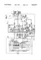
- FIG. 1shows a logic block of the type discussed in U.S. Pat. No. 4,706,216.
- 8-bit RAM 108provides a configurable function of the address bits A, B, and C on lines 110-1, 110-2, and 110-3 respectively.
- Multiplexers 112, 113, 114, 123,126, 127, and 128determine whether one of the 8 bits in RAM 108 will be forwarded.
- XOR gates 124, 129, and 130determine whether the outputs of multiplexers 123, 127, and 128 respectively will be inverted, and AND gates 125, 131, and 132 determine whether the respective outputs of the XOR gates will be passed to a terminal of storage device 121.
- a control signalmust be provided to each of these multiplexers, XOR gates and AND gates.
- a means of storing the signalmust be provided, such as a memory cell.
- a second 8-bit RAM 109can also be configured to provide another function of the inputs A, B and C.
- Input signal Dcauses multiplexer 112 to select between the two functions.
- the logic block of FIG. 1can provide a selectable function of the inputs A, B, C, and D. It frequently occurs that a user may partition logic into the chip so that only three inputs, for example A, B, and C are used in a particular logic block, and that the D input is not used (tied to a constant value rather than connected to receive a logic signal). In this case it is not necessary to use both 8-bit RAMs 108 and 109 since either RAM could provide all functions of three inputs. Thus some silicon area which has been dedicated to the second 8-bit RAM is not used.
- the present inventionis used in a logic array which comprises a plurality of logic blocks.
- Each logic blockmay in a first or default mode calculate a larger number of functions of a maximum number of variables.
- the logic blockmay calculate a smaller number of functions of one less variable. Since the mode of each block is separately selected, the chip offers a good combination of gate density and function flexibility.
- the present inventionallows for some memory bits which in the prior art were used only to represent a function in a look-up table of a logic block to alternately control configuration of some elements such as multiplexers, XOR gates and AND gates. Certain of the multiplexers, XOR gates or AND gates (or other functions in other embodiments) are much more commonly used in one configuration than in another so that it is reasonable to provide a default configuration of these elements.
- a default configurationis provided in which multiple controllable elements are controlled from a single signal. When the elements are to be used in their default configuration, the memory bits which would control them can provide a logic function. When the elements are to be used in a user-selected configuration, an input signal is not used, and the logic function of that input is not provided.
- Means for controlling whether the default condition is used and means for selecting between a default value and a user's valueare provided in the logic block.
- the means for controlling whether the default condition is usedcan be one or a few memory cells, and the means for selecting between the default value and the user's value can be a two-input multiplexer (requires only two transistors).
- the size of a multiplexertwo transistors and the area which must be dedicated to routing signals, the invention can save considerable chip area and thus reduce the cost of the chip.
- FIG. 1shows a prior art logic block which uses memory cells to store a logic function look-up table.
- FIG. 2is a re-drawing of FIG. 1 showing multiplexers and memory cells sized more in proportion to the actual area occupied in a typical integrated circuit device.
- FIG. 3shows a logic block of the present invention which uses some memory cells for the combined function of storing a logic function look-up table and controlling configuration of part of the logic block.
- memory cells 113a and 114aselect the states of multiplexers 113 and 114 respectively. If the logic block of FIG. 1 is being used to compute a function of four variables, A, B, C, and D, memory cells 113a and 114a will cause multiplexers 113 and 114 to select the input from multiplexer 112. Multiplexer 112 is controlled by input signal D, which is treated as the fourth variable to select between the outputs of select generators 110 and 111. If the logic block of FIG. 1 is to generate a function of three variables, or two separate functions of three variables, memory cell 113 will cause multiplexers 113 and 114 to each directly select the output of select units 110 and 111, respectively.
- FIG.2is a redrawing of the logic block of FIG. 1 which differs in the relative sizes of the multiplexers and memory cells and shows these elements in a relationship more close to the physical area actually occupied on the chip.
- the memory cellsoccupy a significant portion of the total area.
- a memory celloccupies a larger portion than a multiplexer.
- the memory for one of the select generatorsis given an alternative purpose of configuring other parts of the logic block to configurations other than their default configuration.
- the present inventionadds one or more memory cells for indicating a default state, but reduces the number of memory cells needed to control certain multiplexers or other controllable elements when those elements are to be operated in their default state.
- the logic blockis used in its default configuration, the memory cells which are not needed to configure the block are available to generate a function.
- FIG. 3shows a logic block according to the present invention in which additional memory cell S1 indicates whether the logic block is to be used in its default mode, providing a function of four variables, A, B, C, and D but configured in its default configuration, or whether it is to provide a function of three variables, for example A, B, and C, but configured in a user selected configuration.
- Memory cells 108a through 108hprovide the dual function of generating a function of three of the four variables A, B, C, and D or of configuring certain of the multiplexers in the remainder of the logic block.
- memory cell 108astores a 0 or 1, which can be provided as a function to the inputs of multiplexers 112 and 113 in response to a particular address provided on lines 110-1, 110-2, and 110-3 which are driven by signals on input lines A, B, C.
- the value in memory cell 108awhich is output on line C0, also provides an input to multiplexer M0, for controlling multiplexer 128 when multiplexer M0 is not in its default mode.
- added memory cell S1causes multiplexer M0 to provide a constant value K0, either high or low, to the control terminal of multiplexer 128, thus placing multiplexer 128 into its default mode.
- lines C1 through C7 from memory cells 108b through 108halso provide configuration control signals to multiplexers M1 through M7 respectively, which are operated in their default mode in response to a first value in memory cell S1 and are operated in a user selected mode when a second value is stored in memory cell S1.
- the embodiment shown in FIG. 3eliminates the set and reset controls and the D input disable in the default mode, and is only one of many embodiments of the present invention.
- the default connection to high or low voltage(represented by K0 through K7 in FIG. 3) is not a configuration choice of the user. It is a permanent connection made when the chip is manufactured.
- multiplexers and controllable elementscan be provided in a logic cell and alternatively controlled through a select multiplexer to operate in a default mode or in a user-selected mode.
- the particular multiplexers or other controllable elements which are alternatively operated in a default or a user selected modeshould be those which can tolerate the reduced flexibility of user control most easily.
Landscapes
- Physics & Mathematics (AREA)
- Engineering & Computer Science (AREA)
- Computer Hardware Design (AREA)
- Computing Systems (AREA)
- General Engineering & Computer Science (AREA)
- Mathematical Physics (AREA)
- Logic Circuits (AREA)
Abstract
Description
This application is a continuation of application Ser. No. 07/994,002, filed Dec. 21, 1992.
The invention relates to field programmable integrated circuit devices, more particularly to field programmable gate arrays in which internal logic blocks are configured partly by loading a memory and partly by setting certain configuration bits.
Field programmable gate arrays (FPGAs) are user programmable logic devices formed in integrated circuit chips, which include within them configurable logic blocks and a configurable interconnect structure. By configuring the chip, the logic blocks can each be made to perform a selected one of many functions, and the interconnect can be connected to route signals from one logic block and to points exterior to the chip. Thus the FPGA can be programmed or configured to perform a desired complex function and provide output signals at selected exterior pins as specified by the user. Some FPGAs are non-volatile and one-time programmable. Others are reprogrammable. Some have logic blocks configured by applying particular signals to logic gate inputs or multiplexer control inputs. Others are configured by applying a combination of signals to logic gate inputs or multiplexer controls and loading a sequence of bits into a memory. The memory provides a logic function of signals on memory address lines, the function being determined by the set of values loaded into the bits of the memory. Such devices are manufactured by Xilinx, Inc., assignee of the present invention, and are described more thoroughly in the 1992 "The Programmable Gate Array Data Book" available from Xilinx, Inc., 2100 Logic Drive, San Jose, Calif. 95124. Such devices are also described in U.S. Pat. Nos. 4,870,302, and 4,706,216 incorporated herein by reference. FIG. 8 of the '216 patent in particular, describes a logic block which is configured by loading bits in a memory and configuring certain multiplexers, exclusive-or gates and AND gates to respond in particular ways to other input signals.
FIG. 1 shows a logic block of the type discussed in U.S. Pat. No. 4,706,216. 8-bit RAM 108 provides a configurable function of the address bits A, B, and C on lines 110-1, 110-2, and 110-3 respectively.Multiplexers RAM 108 will be forwarded.XOR gates multiplexers gates storage device 121. In order to select the desired option, a control signal must be provided to each of these multiplexers, XOR gates and AND gates. Thus, a means of storing the signal must be provided, such as a memory cell.
In FIG. 1, a second 8-bit RAM 109 can also be configured to provide another function of the inputs A, B and C. Input signal D causesmultiplexer 112 to select between the two functions. Thus the logic block of FIG. 1 can provide a selectable function of the inputs A, B, C, and D. It frequently occurs that a user may partition logic into the chip so that only three inputs, for example A, B, and C are used in a particular logic block, and that the D input is not used (tied to a constant value rather than connected to receive a logic signal). In this case it is not necessary to use both 8-bit RAMs
The present invention is used in a logic array which comprises a plurality of logic blocks. Each logic block may in a first or default mode calculate a larger number of functions of a maximum number of variables. In a second or fully configurable mode the logic block may calculate a smaller number of functions of one less variable. Since the mode of each block is separately selected, the chip offers a good combination of gate density and function flexibility.
It is always preferable to implement logic in the smallest silicon area possible in order to save cost and increase speed. The present invention allows for some memory bits which in the prior art were used only to represent a function in a look-up table of a logic block to alternately control configuration of some elements such as multiplexers, XOR gates and AND gates. Certain of the multiplexers, XOR gates or AND gates (or other functions in other embodiments) are much more commonly used in one configuration than in another so that it is reasonable to provide a default configuration of these elements. According to the invention, a default configuration is provided in which multiple controllable elements are controlled from a single signal. When the elements are to be used in their default configuration, the memory bits which would control them can provide a logic function. When the elements are to be used in a user-selected configuration, an input signal is not used, and the logic function of that input is not provided.
Means for controlling whether the default condition is used and means for selecting between a default value and a user's value are provided in the logic block. The means for controlling whether the default condition is used can be one or a few memory cells, and the means for selecting between the default value and the user's value can be a two-input multiplexer (requires only two transistors). Depending upon the size of a memory cell (five transistors in an embodiment described in U.S. Pat. No. 4,750,155 for example), the size of a multiplexer (two transistors) and the area which must be dedicated to routing signals, the invention can save considerable chip area and thus reduce the cost of the chip.
FIG. 1 shows a prior art logic block which uses memory cells to store a logic function look-up table.
FIG. 2 is a re-drawing of FIG. 1 showing multiplexers and memory cells sized more in proportion to the actual area occupied in a typical integrated circuit device.
FIG. 3 shows a logic block of the present invention which uses some memory cells for the combined function of storing a logic function look-up table and controlling configuration of part of the logic block.
As was shown in FIG. 1,memory cells multiplexers memory cells multiplexers multiplexer 112.Multiplexer 112 is controlled by input signal D, which is treated as the fourth variable to select between the outputs ofselect generators memory cell 113 will causemultiplexers select units select generators storage device 121 may most frequently be configured to disable the set and reset functions. Likewise, most frequently, the output ofmultiplexer 114, rather than a constant high or low signal will be provided to the D input ofstorage device 121. Other parts of the logic block may be operated in a particular mode most of the time, for example the clock input CK may most often be driven using the CLK input.
FIG.2 is a redrawing of the logic block of FIG. 1 which differs in the relative sizes of the multiplexers and memory cells and shows these elements in a relationship more close to the physical area actually occupied on the chip. As can be seen in FIG. 2, the memory cells occupy a significant portion of the total area. In particular, a memory cell occupies a larger portion than a multiplexer. (Memory cells take on the order of five transistors, whereas multiplexers take as few as two transistors.) Thus it becomes clear from looking at the relative sizes in FIG. 2 that total chip area can be saved by reducing the number of memory cells.
According to the present invention, when less than the maximum number of variables are being used in one of the logic blocks, the memory for one of the select generators is given an alternative purpose of configuring other parts of the logic block to configurations other than their default configuration. Thus the number of memory cells needed to configure the chip is reduced. The present invention adds one or more memory cells for indicating a default state, but reduces the number of memory cells needed to control certain multiplexers or other controllable elements when those elements are to be operated in their default state. When the logic block is used in its default configuration, the memory cells which are not needed to configure the block are available to generate a function.
FIG. 3 shows a logic block according to the present invention in which additional memory cell S1 indicates whether the logic block is to be used in its default mode, providing a function of four variables, A, B, C, and D but configured in its default configuration, or whether it is to provide a function of three variables, for example A, B, and C, but configured in a user selected configuration.Memory cells 108a through 108h provide the dual function of generating a function of three of the four variables A, B, C, and D or of configuring certain of the multiplexers in the remainder of the logic block. For example,memory cell 108a stores a 0 or 1, which can be provided as a function to the inputs ofmultiplexers memory cell 108a, which is output on line C0, also provides an input to multiplexer M0, for controllingmultiplexer 128 when multiplexer M0 is not in its default mode. Whenmultiplexer 128 is in its default mode, added memory cell S1 causes multiplexer M0 to provide a constant value K0, either high or low, to the control terminal ofmultiplexer 128, thus placingmultiplexer 128 into its default mode. Thus thememory cell 128a which was provided in the prior art embodiment of FIG. 2 has been replaced by multiplexer M0, input line CO and the connection K0 to high or low voltage. This replacement occupies considerably less area than the original cell, and therefore saves total chip area. Likewise, lines C1 through C7 frommemory cells 108b through 108h also provide configuration control signals to multiplexers M1 through M7 respectively, which are operated in their default mode in response to a first value in memory cell S1 and are operated in a user selected mode when a second value is stored in memory cell S1. The embodiment shown in FIG. 3 eliminates the set and reset controls and the D input disable in the default mode, and is only one of many embodiments of the present invention. The default connection to high or low voltage (represented by K0 through K7 in FIG. 3) is not a configuration choice of the user. It is a permanent connection made when the chip is manufactured.
Other multiplexers and controllable elements can be provided in a logic cell and alternatively controlled through a select multiplexer to operate in a default mode or in a user-selected mode. The particular multiplexers or other controllable elements which are alternatively operated in a default or a user selected mode should be those which can tolerate the reduced flexibility of user control most easily.
Other embodiments of the present invention will become obvious to those skilled in the art in light of the above description and are intended to be included in the scope of the present invention.
Claims (3)
1. A logic block for a configurable logic array integrated circuit comprising:
a first memory unit (111) having a first plurality of memory bits (109) for generating a first function in response to a first plurality of inputs (A, B, C);
a second memory unit (110) having a second plurality of memory bits (108a-108h) for generating a second function in response to a second plurality of inputs (A, B, C);
at least one multiplexer (M0-M7) which supplies a control signal to a controllable element (i.e. 124, 126) to cause said controllable element to alternatively have a default configuration (set by K0-K7) and a selected configuration (set by C0-C7) configurable by a corresponding at least one memory bit (108a-108h) from said second plurality of memory bits; and
means (S1) for selecting between said default configuration and said selected configuration.
2. A logic block for a configurable logic array integrated circuit comprising:
a first memory unit (111) having a first plurality of memory bits (109) for generating a first function in response to a first plurality of inputs (A, B, C);
a second memory unit (110) having a second plurality of memory bits (108a-108h) for generating a second function in response to a second plurality of inputs (A, B, C);
at least one element (M0-M7) which can alternatively have a default configuration established by connecting an input to high or low voltage (set by K0-K7) and a selected configuration (set by C0-C7) configurable by a corresponding at least one memory bit (108a-108h) from said second plurality of memory bits; and
means (S1) for selecting between said default configuration and said selected configuration;
in which:
said at least one element which can alternatively have a default configuration is a plurality of elements less than or equal in number to the number of said second plurality of bits; and
said at least one of said bits in said second plurality of memory bits is all of said second plurality of memory bits.
3. A logic block as in claim 2 in which:
said at least one element which can alternatively have a default configuration is a plurality of elements equal in number to the number of said second plurality of bits.
Priority Applications (1)
| Application Number | Priority Date | Filing Date | Title |
|---|---|---|---|
| US08/324,858US5414377A (en) | 1992-12-21 | 1994-10-18 | Logic block with look-up table for configuration and memory |
Applications Claiming Priority (2)
| Application Number | Priority Date | Filing Date | Title |
|---|---|---|---|
| US99400292A | 1992-12-21 | 1992-12-21 | |
| US08/324,858US5414377A (en) | 1992-12-21 | 1994-10-18 | Logic block with look-up table for configuration and memory |
Related Parent Applications (1)
| Application Number | Title | Priority Date | Filing Date |
|---|---|---|---|
| US99400292AContinuation | 1992-12-21 | 1992-12-21 |
Publications (1)
| Publication Number | Publication Date |
|---|---|
| US5414377Atrue US5414377A (en) | 1995-05-09 |
Family
ID=25540182
Family Applications (1)
| Application Number | Title | Priority Date | Filing Date |
|---|---|---|---|
| US08/324,858Expired - LifetimeUS5414377A (en) | 1992-12-21 | 1994-10-18 | Logic block with look-up table for configuration and memory |
Country Status (1)
| Country | Link |
|---|---|
| US (1) | US5414377A (en) |
Cited By (67)
| Publication number | Priority date | Publication date | Assignee | Title |
|---|---|---|---|---|
| US5473267A (en)* | 1993-02-16 | 1995-12-05 | Sgs-Thomson Microelectronics Limited | Programmable logic device with memory that can store routing data of logic data |
| US5546018A (en)* | 1993-09-02 | 1996-08-13 | Xilinx, Inc. | Fast carry structure with synchronous input |
| US5594367A (en)* | 1995-10-16 | 1997-01-14 | Xilinx, Inc. | Output multiplexer within input/output circuit for time multiplexing and high speed logic |
| US5719889A (en)* | 1995-12-20 | 1998-02-17 | International Business Machines Corporation | Programmable parity checking and comparison circuit |
| US5737766A (en)* | 1996-02-14 | 1998-04-07 | Hewlett Packard Company | Programmable gate array configuration memory which allows sharing with user memory |
| US5742180A (en)* | 1995-02-10 | 1998-04-21 | Massachusetts Institute Of Technology | Dynamically programmable gate array with multiple contexts |
| US5796269A (en)* | 1996-04-09 | 1998-08-18 | Xilinx, Inc. | Composable memory array for a programmable logic device and method for implementing same |
| US5821773A (en)* | 1995-09-06 | 1998-10-13 | Altera Corporation | Look-up table based logic element with complete permutability of the inputs to the secondary signals |
| US5844422A (en)* | 1996-11-13 | 1998-12-01 | Xilinx, Inc. | State saving and restoration in reprogrammable FPGAs |
| US5889413A (en)* | 1996-11-22 | 1999-03-30 | Xilinx, Inc. | Lookup tables which double as shift registers |
| US5894565A (en)* | 1996-05-20 | 1999-04-13 | Atmel Corporation | Field programmable gate array with distributed RAM and increased cell utilization |
| US5898319A (en)* | 1993-09-02 | 1999-04-27 | Xilinx, Inc. | Method and structure for providing fast conditional sum in a field programmable gate array |
| US5920202A (en)* | 1997-02-26 | 1999-07-06 | Xilinx, Inc. | Configurable logic element with ability to evaluate five and six input functions |
| US5924115A (en)* | 1996-03-29 | 1999-07-13 | Interval Research Corporation | Hierarchical memory architecture for a programmable integrated circuit having an interconnect structure connected in a tree configuration |
| US5936426A (en) | 1997-02-03 | 1999-08-10 | Actel Corporation | Logic function module for field programmable array |
| US5977791A (en)* | 1996-04-15 | 1999-11-02 | Altera Corporation | Embedded memory block with FIFO mode for programmable logic device |
| US6011744A (en)* | 1997-07-16 | 2000-01-04 | Altera Corporation | Programmable logic device with multi-port memory |
| US6018490A (en)* | 1991-09-03 | 2000-01-25 | Altera Corporation | Programmable logic array integrated circuits |
| US6020760A (en)* | 1997-07-16 | 2000-02-01 | Altera Corporation | I/O buffer circuit with pin multiplexing |
| US6029236A (en)* | 1997-01-28 | 2000-02-22 | Altera Corporation | Field programmable gate array with high speed SRAM based configurable function block configurable as high performance logic or block of SRAM |
| US6034857A (en)* | 1997-07-16 | 2000-03-07 | Altera Corporation | Input/output buffer with overcurrent protection circuit |
| US6049223A (en)* | 1995-03-22 | 2000-04-11 | Altera Corporation | Programmable logic array integrated circuit with general-purpose memory configurable as a random access or FIFO memory |
| US6073222A (en)* | 1994-10-13 | 2000-06-06 | Vinca Corporation | Using a virtual device to access data as it previously existed in a mass data storage system |
| US6104207A (en)* | 1998-04-27 | 2000-08-15 | Lattice Semiconductor Corporation | Programmable logic device |
| US6134166A (en)* | 1995-03-22 | 2000-10-17 | Altera Corporation | Programmable logic array integrated circuit incorporating a first-in first-out memory |
| US6154053A (en)* | 1993-09-02 | 2000-11-28 | Xilinx, Inc. | Look-ahead carry structure with homogeneous CLB structure and pitch larger than CLB pitch |
| US6184709B1 (en) | 1996-04-09 | 2001-02-06 | Xilinx, Inc. | Programmable logic device having a composable memory array overlaying a CLB array |
| US6184707B1 (en) | 1998-10-07 | 2001-02-06 | Altera Corporation | Look-up table based logic element with complete permutability of the inputs to the secondary signals |
| US6201410B1 (en) | 1997-02-26 | 2001-03-13 | Xilinx, Inc. | Wide logic gate implemented in an FPGA configurable logic element |
| US6249143B1 (en) | 1997-05-23 | 2001-06-19 | Altera Corporation | Programmable logic array integrated circuit with distributed random access memory array |
| US6255846B1 (en)* | 1997-10-16 | 2001-07-03 | Altera Corporation | Programmable logic devices with enhanced multiplexing capabilities |
| US6262933B1 (en) | 1999-01-29 | 2001-07-17 | Altera Corporation | High speed programmable address decoder |
| US6288568B1 (en) | 1996-11-22 | 2001-09-11 | Xilinx, Inc. | FPGA architecture with deep look-up table RAMs |
| US6288570B1 (en) | 1993-09-02 | 2001-09-11 | Xilinx, Inc. | Logic structure and circuit for fast carry |
| US6297665B1 (en) | 1996-11-22 | 2001-10-02 | Xilinx, Inc. | FPGA architecture with dual-port deep look-up table RAMS |
| US6323682B1 (en) | 1996-11-22 | 2001-11-27 | Xilinx, Inc. | FPGA architecture with wide function multiplexers |
| US20010049816A1 (en)* | 1999-12-30 | 2001-12-06 | Adaptive Silicon, Inc. | Multi-scale programmable array |
| US6342792B1 (en)* | 1999-03-04 | 2002-01-29 | Altera Corporation | Logic module circuitry for programmable logic devices |
| US6346824B1 (en) | 1996-04-09 | 2002-02-12 | Xilinx, Inc. | Dedicated function fabric for use in field programmable gate arrays |
| US6356110B1 (en) | 2000-04-03 | 2002-03-12 | Altera Corporation San Jose Ca | Multifunction memory array in a programmable logic device |
| US6400180B2 (en)* | 1999-02-25 | 2002-06-04 | Xilinix, Inc. | Configurable lookup table for programmable logic devices |
| US6411124B2 (en) | 2000-04-28 | 2002-06-25 | Altera Corporation | Programmable logic device logic modules with shift register capabilities |
| US6448808B2 (en) | 1997-02-26 | 2002-09-10 | Xilinx, Inc. | Interconnect structure for a programmable logic device |
| US20020130681A1 (en)* | 1991-09-03 | 2002-09-19 | Cliff Richard G. | Programmable logic array integrated circuits |
| US6462577B1 (en) | 2000-04-28 | 2002-10-08 | Altera Corporation | Configurable memory structures in a programmable logic device |
| US6467017B1 (en) | 1998-06-23 | 2002-10-15 | Altera Corporation | Programmable logic device having embedded dual-port random access memory configurable as single-port memory |
| US6486702B1 (en) | 1999-07-02 | 2002-11-26 | Altera Corporation | Embedded memory blocks for programmable logic |
| US6501296B2 (en) | 1999-02-25 | 2002-12-31 | Xilinx, Inc. | Logic/memory circuit having a plurality of operating modes |
| US6529040B1 (en)* | 2000-05-05 | 2003-03-04 | Xilinx, Inc. | FPGA lookup table with speed read decoder |
| US20030055852A1 (en)* | 2001-09-19 | 2003-03-20 | Wojko Mathew Francis | Reconfigurable arithmetic logic block array for FPGAs |
| US6720796B1 (en) | 2001-05-06 | 2004-04-13 | Altera Corporation | Multiple size memories in a programmable logic device |
| US6724810B1 (en) | 2000-11-17 | 2004-04-20 | Xilinx, Inc. | Method and apparatus for de-spreading spread spectrum signals |
| US6759870B2 (en) | 1991-09-03 | 2004-07-06 | Altera Corporation | Programmable logic array integrated circuits |
| US20040193852A1 (en)* | 2003-03-31 | 2004-09-30 | Johnson Scott D. | Extension adapter |
| US20040194048A1 (en)* | 2003-03-31 | 2004-09-30 | Arnold Jeffrey M. | System and method for efficiently mapping heterogeneous objects onto an array of heterogeneous programmable logic resources |
| US20050027970A1 (en)* | 2003-07-29 | 2005-02-03 | Arnold Jeffrey Mark | Reconfigurable instruction set computing |
| US6857043B1 (en)* | 2000-04-28 | 2005-02-15 | Altera Corporation | Shift register implementations of first-in/first-out memories utilizing a double increment gray code counter |
| US20050114565A1 (en)* | 2003-03-31 | 2005-05-26 | Stretch, Inc. | Systems and methods for selecting input/output configuration in an integrated circuit |
| US7084665B1 (en) | 2004-07-22 | 2006-08-01 | Altera Corporation | Distributed random access memory in a programmable logic device |
| US7111110B1 (en) | 2002-12-10 | 2006-09-19 | Altera Corporation | Versatile RAM for programmable logic device |
| US20060259747A1 (en)* | 2003-07-29 | 2006-11-16 | Stretch, Inc. | Long instruction word processing with instruction extensions |
| US20070146178A1 (en)* | 2005-12-27 | 2007-06-28 | David Lewis | Distributed memory in field-programmable gate array integrated circuit devices |
| US7581081B2 (en) | 2003-03-31 | 2009-08-25 | Stretch, Inc. | Systems and methods for software extensible multi-processing |
| US8001266B1 (en) | 2003-03-31 | 2011-08-16 | Stretch, Inc. | Configuring a multi-processor system |
| US8832326B1 (en)* | 2005-11-01 | 2014-09-09 | Xilinx, Inc. | Circuit and method for ordering data words |
| EP3157171A1 (en) | 2015-10-15 | 2017-04-19 | Menta | Logic block architecture for programmable gate array |
| US20180145497A1 (en)* | 2016-11-23 | 2018-05-24 | Schneider Electric USA, Inc. | Method to utilize multiple configuration software for df/cafi breakers |
Citations (4)
| Publication number | Priority date | Publication date | Assignee | Title |
|---|---|---|---|---|
| US4706216A (en)* | 1985-02-27 | 1987-11-10 | Xilinx, Inc. | Configurable logic element |
| US4870302A (en)* | 1984-03-12 | 1989-09-26 | Xilinx, Inc. | Configurable electrical circuit having configurable logic elements and configurable interconnects |
| US5245227A (en)* | 1990-11-02 | 1993-09-14 | Atmel Corporation | Versatile programmable logic cell for use in configurable logic arrays |
| US5245226A (en)* | 1991-02-25 | 1993-09-14 | Lattice Semiconductor Corporation | Output logic macrocell |
- 1994
- 1994-10-18USUS08/324,858patent/US5414377A/ennot_activeExpired - Lifetime
Patent Citations (4)
| Publication number | Priority date | Publication date | Assignee | Title |
|---|---|---|---|---|
| US4870302A (en)* | 1984-03-12 | 1989-09-26 | Xilinx, Inc. | Configurable electrical circuit having configurable logic elements and configurable interconnects |
| US4706216A (en)* | 1985-02-27 | 1987-11-10 | Xilinx, Inc. | Configurable logic element |
| US5245227A (en)* | 1990-11-02 | 1993-09-14 | Atmel Corporation | Versatile programmable logic cell for use in configurable logic arrays |
| US5245226A (en)* | 1991-02-25 | 1993-09-14 | Lattice Semiconductor Corporation | Output logic macrocell |
Non-Patent Citations (1)
| Title |
|---|
| Xilinx Programmable Gate Array Data Book, 1992, available from Xilinx, Inc. 2100 Logic Drive, San Jose Calif. 95124.* |
Cited By (114)
| Publication number | Priority date | Publication date | Assignee | Title |
|---|---|---|---|---|
| US6023439A (en)* | 1991-09-03 | 2000-02-08 | Altera Corporation | Programmable logic array integrated circuits |
| US6759870B2 (en) | 1991-09-03 | 2004-07-06 | Altera Corporation | Programmable logic array integrated circuits |
| US6134173A (en)* | 1991-09-03 | 2000-10-17 | Altera Corporation | Programmable logic array integrated circuits |
| US20020130681A1 (en)* | 1991-09-03 | 2002-09-19 | Cliff Richard G. | Programmable logic array integrated circuits |
| US6064599A (en)* | 1991-09-03 | 2000-05-16 | Altera Corporation | Programmable logic array integrated circuits |
| US6897679B2 (en) | 1991-09-03 | 2005-05-24 | Altera Corporation | Programmable logic array integrated circuits |
| US20040066212A1 (en)* | 1991-09-03 | 2004-04-08 | Altera Corporation | Programmable logic array integrated circuits |
| US6018490A (en)* | 1991-09-03 | 2000-01-25 | Altera Corporation | Programmable logic array integrated circuits |
| US5473267A (en)* | 1993-02-16 | 1995-12-05 | Sgs-Thomson Microelectronics Limited | Programmable logic device with memory that can store routing data of logic data |
| US6288570B1 (en) | 1993-09-02 | 2001-09-11 | Xilinx, Inc. | Logic structure and circuit for fast carry |
| US6154053A (en)* | 1993-09-02 | 2000-11-28 | Xilinx, Inc. | Look-ahead carry structure with homogeneous CLB structure and pitch larger than CLB pitch |
| US5898319A (en)* | 1993-09-02 | 1999-04-27 | Xilinx, Inc. | Method and structure for providing fast conditional sum in a field programmable gate array |
| US5546018A (en)* | 1993-09-02 | 1996-08-13 | Xilinx, Inc. | Fast carry structure with synchronous input |
| US6073222A (en)* | 1994-10-13 | 2000-06-06 | Vinca Corporation | Using a virtual device to access data as it previously existed in a mass data storage system |
| US5742180A (en)* | 1995-02-10 | 1998-04-21 | Massachusetts Institute Of Technology | Dynamically programmable gate array with multiple contexts |
| US6049223A (en)* | 1995-03-22 | 2000-04-11 | Altera Corporation | Programmable logic array integrated circuit with general-purpose memory configurable as a random access or FIFO memory |
| US6218860B1 (en) | 1995-03-22 | 2001-04-17 | Altera Corporation | Programmable logic array integrated circuit incorporating a first-in first-out memory |
| US6134166A (en)* | 1995-03-22 | 2000-10-17 | Altera Corporation | Programmable logic array integrated circuit incorporating a first-in first-out memory |
| US6340897B1 (en) | 1995-03-22 | 2002-01-22 | Altera Corporation | Programmable logic array integrated circuit with general-purpose memory configurable as a random access or FIFO memory |
| US5821773A (en)* | 1995-09-06 | 1998-10-13 | Altera Corporation | Look-up table based logic element with complete permutability of the inputs to the secondary signals |
| US5594367A (en)* | 1995-10-16 | 1997-01-14 | Xilinx, Inc. | Output multiplexer within input/output circuit for time multiplexing and high speed logic |
| US5719889A (en)* | 1995-12-20 | 1998-02-17 | International Business Machines Corporation | Programmable parity checking and comparison circuit |
| US5737766A (en)* | 1996-02-14 | 1998-04-07 | Hewlett Packard Company | Programmable gate array configuration memory which allows sharing with user memory |
| EP0790706A3 (en)* | 1996-02-14 | 1999-01-07 | Hewlett-Packard Company | Memory system |
| US5924115A (en)* | 1996-03-29 | 1999-07-13 | Interval Research Corporation | Hierarchical memory architecture for a programmable integrated circuit having an interconnect structure connected in a tree configuration |
| US5886538A (en)* | 1996-04-09 | 1999-03-23 | Xilinx, Inc. | Composable memory array for a programmable logic device and method implementing same |
| US6184709B1 (en) | 1996-04-09 | 2001-02-06 | Xilinx, Inc. | Programmable logic device having a composable memory array overlaying a CLB array |
| US6346824B1 (en) | 1996-04-09 | 2002-02-12 | Xilinx, Inc. | Dedicated function fabric for use in field programmable gate arrays |
| US5796269A (en)* | 1996-04-09 | 1998-08-18 | Xilinx, Inc. | Composable memory array for a programmable logic device and method for implementing same |
| US6242946B1 (en) | 1996-04-15 | 2001-06-05 | Altera Corporation | Embedded memory block with FIFO mode for programmable logic device |
| US5977791A (en)* | 1996-04-15 | 1999-11-02 | Altera Corporation | Embedded memory block with FIFO mode for programmable logic device |
| US6292021B1 (en) | 1996-05-20 | 2001-09-18 | Atmel Corporation | FPGA structure having main, column and sector reset lines |
| US6026227A (en)* | 1996-05-20 | 2000-02-15 | Atmel Corporation | FPGA logic cell internal structure including pair of look-up tables |
| US6014509A (en)* | 1996-05-20 | 2000-01-11 | Atmel Corporation | Field programmable gate array having access to orthogonal and diagonal adjacent neighboring cells |
| US5894565A (en)* | 1996-05-20 | 1999-04-13 | Atmel Corporation | Field programmable gate array with distributed RAM and increased cell utilization |
| US6167559A (en)* | 1996-05-20 | 2000-12-26 | Atmel Corporation | FPGA structure having main, column and sector clock lines |
| US5844422A (en)* | 1996-11-13 | 1998-12-01 | Xilinx, Inc. | State saving and restoration in reprogrammable FPGAs |
| US6323682B1 (en) | 1996-11-22 | 2001-11-27 | Xilinx, Inc. | FPGA architecture with wide function multiplexers |
| US6288568B1 (en) | 1996-11-22 | 2001-09-11 | Xilinx, Inc. | FPGA architecture with deep look-up table RAMs |
| US6118298A (en)* | 1996-11-22 | 2000-09-12 | Xilinx, Inc. | Structure for optionally cascading shift registers |
| US5889413A (en)* | 1996-11-22 | 1999-03-30 | Xilinx, Inc. | Lookup tables which double as shift registers |
| US6297665B1 (en) | 1996-11-22 | 2001-10-02 | Xilinx, Inc. | FPGA architecture with dual-port deep look-up table RAMS |
| US6262597B1 (en) | 1996-11-22 | 2001-07-17 | Xilinx, Inc. | FIFO in FPGA having logic elements that include cascadable shift registers |
| US6029236A (en)* | 1997-01-28 | 2000-02-22 | Altera Corporation | Field programmable gate array with high speed SRAM based configurable function block configurable as high performance logic or block of SRAM |
| US5936426A (en) | 1997-02-03 | 1999-08-10 | Actel Corporation | Logic function module for field programmable array |
| US6124731A (en)* | 1997-02-26 | 2000-09-26 | Xilinx, Inc. | Configurable logic element with ability to evaluate wide logic functions |
| US6448808B2 (en) | 1997-02-26 | 2002-09-10 | Xilinx, Inc. | Interconnect structure for a programmable logic device |
| US6201410B1 (en) | 1997-02-26 | 2001-03-13 | Xilinx, Inc. | Wide logic gate implemented in an FPGA configurable logic element |
| US5920202A (en)* | 1997-02-26 | 1999-07-06 | Xilinx, Inc. | Configurable logic element with ability to evaluate five and six input functions |
| US6051992A (en)* | 1997-02-26 | 2000-04-18 | Xilinx, Inc. | Configurable logic element with ability to evaluate five and six input functions |
| US6249143B1 (en) | 1997-05-23 | 2001-06-19 | Altera Corporation | Programmable logic array integrated circuit with distributed random access memory array |
| US6011730A (en)* | 1997-07-16 | 2000-01-04 | Altera Corporation | Programmable logic device with multi-port memory |
| US6011744A (en)* | 1997-07-16 | 2000-01-04 | Altera Corporation | Programmable logic device with multi-port memory |
| US6034857A (en)* | 1997-07-16 | 2000-03-07 | Altera Corporation | Input/output buffer with overcurrent protection circuit |
| US6259588B1 (en) | 1997-07-16 | 2001-07-10 | Altera Corporation | Input/output buffer with overcurrent protection circuit |
| US6285211B1 (en) | 1997-07-16 | 2001-09-04 | Altera Corporation | I/O buffer circuit with pin multiplexing |
| US6219284B1 (en) | 1997-07-16 | 2001-04-17 | Altera Corporation | Programmable logic device with multi-port memory |
| US6020760A (en)* | 1997-07-16 | 2000-02-01 | Altera Corporation | I/O buffer circuit with pin multiplexing |
| US6151258A (en)* | 1997-07-16 | 2000-11-21 | Quickturn Design Systems, Inc. | Programmable logic device with multi-port memory |
| US6255846B1 (en)* | 1997-10-16 | 2001-07-03 | Altera Corporation | Programmable logic devices with enhanced multiplexing capabilities |
| US6104207A (en)* | 1998-04-27 | 2000-08-15 | Lattice Semiconductor Corporation | Programmable logic device |
| US6467017B1 (en) | 1998-06-23 | 2002-10-15 | Altera Corporation | Programmable logic device having embedded dual-port random access memory configurable as single-port memory |
| US6184707B1 (en) | 1998-10-07 | 2001-02-06 | Altera Corporation | Look-up table based logic element with complete permutability of the inputs to the secondary signals |
| US6262933B1 (en) | 1999-01-29 | 2001-07-17 | Altera Corporation | High speed programmable address decoder |
| US6459303B1 (en) | 1999-01-29 | 2002-10-01 | Altera Corporation | High speed programmable address decoder |
| US6400180B2 (en)* | 1999-02-25 | 2002-06-04 | Xilinix, Inc. | Configurable lookup table for programmable logic devices |
| US6501296B2 (en) | 1999-02-25 | 2002-12-31 | Xilinx, Inc. | Logic/memory circuit having a plurality of operating modes |
| US6342792B1 (en)* | 1999-03-04 | 2002-01-29 | Altera Corporation | Logic module circuitry for programmable logic devices |
| US6486702B1 (en) | 1999-07-02 | 2002-11-26 | Altera Corporation | Embedded memory blocks for programmable logic |
| US6593772B2 (en) | 1999-07-02 | 2003-07-15 | Altera Corporation | Embedded memory blocks for programmable logic |
| US7062520B2 (en) | 1999-12-30 | 2006-06-13 | Stretch, Inc. | Multi-scale programmable array |
| US6633181B1 (en)* | 1999-12-30 | 2003-10-14 | Stretch, Inc. | Multi-scale programmable array |
| US20010049816A1 (en)* | 1999-12-30 | 2001-12-06 | Adaptive Silicon, Inc. | Multi-scale programmable array |
| US6356110B1 (en) | 2000-04-03 | 2002-03-12 | Altera Corporation San Jose Ca | Multifunction memory array in a programmable logic device |
| US6462577B1 (en) | 2000-04-28 | 2002-10-08 | Altera Corporation | Configurable memory structures in a programmable logic device |
| US6411124B2 (en) | 2000-04-28 | 2002-06-25 | Altera Corporation | Programmable logic device logic modules with shift register capabilities |
| US6857043B1 (en)* | 2000-04-28 | 2005-02-15 | Altera Corporation | Shift register implementations of first-in/first-out memories utilizing a double increment gray code counter |
| US6529040B1 (en)* | 2000-05-05 | 2003-03-04 | Xilinx, Inc. | FPGA lookup table with speed read decoder |
| US6621296B2 (en) | 2000-05-05 | 2003-09-16 | Xilinx, Inc. | FPGA lookup table with high speed read decorder |
| US6724810B1 (en) | 2000-11-17 | 2004-04-20 | Xilinx, Inc. | Method and apparatus for de-spreading spread spectrum signals |
| US6720796B1 (en) | 2001-05-06 | 2004-04-13 | Altera Corporation | Multiple size memories in a programmable logic device |
| US20030055852A1 (en)* | 2001-09-19 | 2003-03-20 | Wojko Mathew Francis | Reconfigurable arithmetic logic block array for FPGAs |
| US7111110B1 (en) | 2002-12-10 | 2006-09-19 | Altera Corporation | Versatile RAM for programmable logic device |
| US7480763B2 (en) | 2002-12-10 | 2009-01-20 | Altera Corporation | Versatile RAM for a programmable logic device |
| US8001266B1 (en) | 2003-03-31 | 2011-08-16 | Stretch, Inc. | Configuring a multi-processor system |
| US7613900B2 (en) | 2003-03-31 | 2009-11-03 | Stretch, Inc. | Systems and methods for selecting input/output configuration in an integrated circuit |
| US7590829B2 (en) | 2003-03-31 | 2009-09-15 | Stretch, Inc. | Extension adapter |
| US20040193852A1 (en)* | 2003-03-31 | 2004-09-30 | Johnson Scott D. | Extension adapter |
| US20050114565A1 (en)* | 2003-03-31 | 2005-05-26 | Stretch, Inc. | Systems and methods for selecting input/output configuration in an integrated circuit |
| US7581081B2 (en) | 2003-03-31 | 2009-08-25 | Stretch, Inc. | Systems and methods for software extensible multi-processing |
| US20040194048A1 (en)* | 2003-03-31 | 2004-09-30 | Arnold Jeffrey M. | System and method for efficiently mapping heterogeneous objects onto an array of heterogeneous programmable logic resources |
| US7000211B2 (en) | 2003-03-31 | 2006-02-14 | Stretch, Inc. | System and method for efficiently mapping heterogeneous objects onto an array of heterogeneous programmable logic resources |
| US6954845B2 (en) | 2003-07-29 | 2005-10-11 | Stretch, Inc. | Reconfigurable instruction set computing |
| US20050273581A1 (en)* | 2003-07-29 | 2005-12-08 | Stretch, Inc. | Programmable logic configuration for instruction extensions |
| US20060259747A1 (en)* | 2003-07-29 | 2006-11-16 | Stretch, Inc. | Long instruction word processing with instruction extensions |
| US20050027970A1 (en)* | 2003-07-29 | 2005-02-03 | Arnold Jeffrey Mark | Reconfigurable instruction set computing |
| US7284114B2 (en) | 2003-07-29 | 2007-10-16 | Stretch, Inc. | Video processing system with reconfigurable instructions |
| US20050027971A1 (en)* | 2003-07-29 | 2005-02-03 | Williams Kenneth M. | Defining instruction extensions in a standard programming language |
| US7373642B2 (en) | 2003-07-29 | 2008-05-13 | Stretch, Inc. | Defining instruction extensions in a standard programming language |
| US7610475B2 (en) | 2003-07-29 | 2009-10-27 | Stretch, Inc. | Programmable logic configuration for instruction extensions |
| US7418575B2 (en) | 2003-07-29 | 2008-08-26 | Stretch, Inc. | Long instruction word processing with instruction extensions |
| US7421561B2 (en) | 2003-07-29 | 2008-09-02 | Stretch, Inc. | Instruction set for efficient bit stream and byte stream I/O |
| US20050027944A1 (en)* | 2003-07-29 | 2005-02-03 | Williams Kenneth Mark | Instruction set for efficient bit stream and byte stream I/O |
| US20050169550A1 (en)* | 2003-07-29 | 2005-08-04 | Arnold Jeffrey M. | Video processing system with reconfigurable instructions |
| US7084665B1 (en) | 2004-07-22 | 2006-08-01 | Altera Corporation | Distributed random access memory in a programmable logic device |
| US7304499B1 (en) | 2004-07-22 | 2007-12-04 | Altera Corporation | Distributed random access memory in a programmable logic device |
| US8832326B1 (en)* | 2005-11-01 | 2014-09-09 | Xilinx, Inc. | Circuit and method for ordering data words |
| US20080231316A1 (en)* | 2005-12-27 | 2008-09-25 | Altera Corporation | Distributed memory in field-programmable gate array integrated circuit devices |
| US7391236B2 (en) | 2005-12-27 | 2008-06-24 | Altera Corporation | Distributed memory in field-programmable gate array integrated circuit devices |
| US7656191B2 (en) | 2005-12-27 | 2010-02-02 | Altera Corporation | Distributed memory in field-programmable gate array integrated circuit devices |
| US20070146178A1 (en)* | 2005-12-27 | 2007-06-28 | David Lewis | Distributed memory in field-programmable gate array integrated circuit devices |
| EP3157171A1 (en) | 2015-10-15 | 2017-04-19 | Menta | Logic block architecture for programmable gate array |
| WO2017063956A1 (en) | 2015-10-15 | 2017-04-20 | Menta | Logic block architecture for programmable gate array |
| US20180145497A1 (en)* | 2016-11-23 | 2018-05-24 | Schneider Electric USA, Inc. | Method to utilize multiple configuration software for df/cafi breakers |
Similar Documents
| Publication | Publication Date | Title |
|---|---|---|
| US5414377A (en) | Logic block with look-up table for configuration and memory | |
| EP1382120B1 (en) | Fpga logic element with variable-length shift register capability | |
| US5905385A (en) | Memory bits used to couple look up table inputs to facilitate increased availability to routing resources particularly for variable sized look up tables for a field programmable gate array (FPGA) | |
| US5128559A (en) | Logic block for programmable logic devices | |
| US6118298A (en) | Structure for optionally cascading shift registers | |
| EP0410759B1 (en) | Configurable logic array and method | |
| US6292019B1 (en) | Programmable logic device having configurable logic blocks with user-accessible input multiplexers | |
| US4975601A (en) | User-writable random access memory logic block for programmable logic devices | |
| US5473266A (en) | Programmable logic device having fast programmable logic array blocks and a central global interconnect array | |
| US6144220A (en) | FPGA Architecture using multiplexers that incorporate a logic gate | |
| US5121006A (en) | Registered logic macrocell with product term allocation and adjacent product term stealing | |
| US5140193A (en) | Programmable connector for programmable logic device | |
| US4931671A (en) | Multiple array customizable logic device | |
| US5027315A (en) | Programmable logic array using internally generated dynamic logic signals as selection signals for controlling its functions | |
| US5986470A (en) | Programmable logic array integrated circuit devices | |
| US5099150A (en) | Circuit block for programmable logic devices, configurable as a user-writable memory or a logic circuit | |
| JP4388069B2 (en) | Configurable logic circuit device | |
| US6556502B2 (en) | Memory circuitry for programmable logic integrated circuit devices | |
| US6703860B1 (en) | I/O block for a programmable interconnect circuit | |
| US6054871A (en) | Method for self-reconfiguration of logic in a field programmable gate array | |
| US6011740A (en) | Structure and method for providing additional configuration memories on an FPGA | |
| US7154298B1 (en) | Block-oriented architecture for a programmable interconnect circuit | |
| EP0227329A2 (en) | Programmable logic device | |
| US6703862B1 (en) | Efficient loadable registers in programmable logic devices | |
| US7099227B1 (en) | PLD hardwire programming with multiple functional modes |
Legal Events
| Date | Code | Title | Description |
|---|---|---|---|
| STCF | Information on status: patent grant | Free format text:PATENTED CASE | |
| FPAY | Fee payment | Year of fee payment:4 | |
| FPAY | Fee payment | Year of fee payment:8 | |
| FPAY | Fee payment | Year of fee payment:12 | |
| AS | Assignment | Owner name:XILINX, INC., CALIFORNIA Free format text:ASSIGNMENT OF ASSIGNORS INTEREST;ASSIGNOR:FREIDIN, PHILIP M.;REEL/FRAME:023401/0368 Effective date:19921221 |