US5413962A - Multi-level conductor process in VLSI fabrication utilizing an air bridge - Google Patents
Multi-level conductor process in VLSI fabrication utilizing an air bridgeDownload PDFInfo
- Publication number
- US5413962A US5413962AUS08/275,268US27526894AUS5413962AUS 5413962 AUS5413962 AUS 5413962AUS 27526894 AUS27526894 AUS 27526894AUS 5413962 AUS5413962 AUS 5413962A
- Authority
- US
- United States
- Prior art keywords
- layer
- inter
- metal
- forming
- thin envelope
- Prior art date
- Legal status (The legal status is an assumption and is not a legal conclusion. Google has not performed a legal analysis and makes no representation as to the accuracy of the status listed.)
- Expired - Lifetime
Links
Images


Classifications
- H—ELECTRICITY
- H01—ELECTRIC ELEMENTS
- H01L—SEMICONDUCTOR DEVICES NOT COVERED BY CLASS H10
- H01L23/00—Details of semiconductor or other solid state devices
- H01L23/52—Arrangements for conducting electric current within the device in operation from one component to another, i.e. interconnections, e.g. wires, lead frames
- H01L23/522—Arrangements for conducting electric current within the device in operation from one component to another, i.e. interconnections, e.g. wires, lead frames including external interconnections consisting of a multilayer structure of conductive and insulating layers inseparably formed on the semiconductor body
- H01L23/5226—Via connections in a multilevel interconnection structure
- H—ELECTRICITY
- H01—ELECTRIC ELEMENTS
- H01L—SEMICONDUCTOR DEVICES NOT COVERED BY CLASS H10
- H01L21/00—Processes or apparatus adapted for the manufacture or treatment of semiconductor or solid state devices or of parts thereof
- H01L21/70—Manufacture or treatment of devices consisting of a plurality of solid state components formed in or on a common substrate or of parts thereof; Manufacture of integrated circuit devices or of parts thereof
- H01L21/71—Manufacture of specific parts of devices defined in group H01L21/70
- H01L21/768—Applying interconnections to be used for carrying current between separate components within a device comprising conductors and dielectrics
- H01L21/76801—Applying interconnections to be used for carrying current between separate components within a device comprising conductors and dielectrics characterised by the formation and the after-treatment of the dielectrics, e.g. smoothing
- H01L21/7682—Applying interconnections to be used for carrying current between separate components within a device comprising conductors and dielectrics characterised by the formation and the after-treatment of the dielectrics, e.g. smoothing the dielectric comprising air gaps
- H—ELECTRICITY
- H01—ELECTRIC ELEMENTS
- H01L—SEMICONDUCTOR DEVICES NOT COVERED BY CLASS H10
- H01L23/00—Details of semiconductor or other solid state devices
- H01L23/52—Arrangements for conducting electric current within the device in operation from one component to another, i.e. interconnections, e.g. wires, lead frames
- H01L23/522—Arrangements for conducting electric current within the device in operation from one component to another, i.e. interconnections, e.g. wires, lead frames including external interconnections consisting of a multilayer structure of conductive and insulating layers inseparably formed on the semiconductor body
- H01L23/5221—Crossover interconnections
- H—ELECTRICITY
- H01—ELECTRIC ELEMENTS
- H01L—SEMICONDUCTOR DEVICES NOT COVERED BY CLASS H10
- H01L23/00—Details of semiconductor or other solid state devices
- H01L23/52—Arrangements for conducting electric current within the device in operation from one component to another, i.e. interconnections, e.g. wires, lead frames
- H01L23/522—Arrangements for conducting electric current within the device in operation from one component to another, i.e. interconnections, e.g. wires, lead frames including external interconnections consisting of a multilayer structure of conductive and insulating layers inseparably formed on the semiconductor body
- H01L23/5222—Capacitive arrangements or effects of, or between wiring layers
- H—ELECTRICITY
- H01—ELECTRIC ELEMENTS
- H01L—SEMICONDUCTOR DEVICES NOT COVERED BY CLASS H10
- H01L23/00—Details of semiconductor or other solid state devices
- H01L23/52—Arrangements for conducting electric current within the device in operation from one component to another, i.e. interconnections, e.g. wires, lead frames
- H01L23/522—Arrangements for conducting electric current within the device in operation from one component to another, i.e. interconnections, e.g. wires, lead frames including external interconnections consisting of a multilayer structure of conductive and insulating layers inseparably formed on the semiconductor body
- H01L23/532—Arrangements for conducting electric current within the device in operation from one component to another, i.e. interconnections, e.g. wires, lead frames including external interconnections consisting of a multilayer structure of conductive and insulating layers inseparably formed on the semiconductor body characterised by the materials
- H01L23/53204—Conductive materials
- H01L23/53209—Conductive materials based on metals, e.g. alloys, metal silicides
- H01L23/53228—Conductive materials based on metals, e.g. alloys, metal silicides the principal metal being copper
- H01L23/53233—Copper alloys
- H—ELECTRICITY
- H01—ELECTRIC ELEMENTS
- H01L—SEMICONDUCTOR DEVICES NOT COVERED BY CLASS H10
- H01L23/00—Details of semiconductor or other solid state devices
- H01L23/52—Arrangements for conducting electric current within the device in operation from one component to another, i.e. interconnections, e.g. wires, lead frames
- H01L23/522—Arrangements for conducting electric current within the device in operation from one component to another, i.e. interconnections, e.g. wires, lead frames including external interconnections consisting of a multilayer structure of conductive and insulating layers inseparably formed on the semiconductor body
- H01L23/532—Arrangements for conducting electric current within the device in operation from one component to another, i.e. interconnections, e.g. wires, lead frames including external interconnections consisting of a multilayer structure of conductive and insulating layers inseparably formed on the semiconductor body characterised by the materials
- H01L23/53204—Conductive materials
- H01L23/53209—Conductive materials based on metals, e.g. alloys, metal silicides
- H01L23/53242—Conductive materials based on metals, e.g. alloys, metal silicides the principal metal being a noble metal, e.g. gold
- H01L23/53247—Noble-metal alloys
- H—ELECTRICITY
- H01—ELECTRIC ELEMENTS
- H01L—SEMICONDUCTOR DEVICES NOT COVERED BY CLASS H10
- H01L21/00—Processes or apparatus adapted for the manufacture or treatment of semiconductor or solid state devices or of parts thereof
- H01L21/70—Manufacture or treatment of devices consisting of a plurality of solid state components formed in or on a common substrate or of parts thereof; Manufacture of integrated circuit devices or of parts thereof
- H01L21/71—Manufacture of specific parts of devices defined in group H01L21/70
- H01L21/768—Applying interconnections to be used for carrying current between separate components within a device comprising conductors and dielectrics
- H01L21/76801—Applying interconnections to be used for carrying current between separate components within a device comprising conductors and dielectrics characterised by the formation and the after-treatment of the dielectrics, e.g. smoothing
- H01L21/76829—Applying interconnections to be used for carrying current between separate components within a device comprising conductors and dielectrics characterised by the formation and the after-treatment of the dielectrics, e.g. smoothing characterised by the formation of thin functional dielectric layers, e.g. dielectric etch-stop, barrier, capping or liner layers
- H01L21/76831—Applying interconnections to be used for carrying current between separate components within a device comprising conductors and dielectrics characterised by the formation and the after-treatment of the dielectrics, e.g. smoothing characterised by the formation of thin functional dielectric layers, e.g. dielectric etch-stop, barrier, capping or liner layers in via holes or trenches, e.g. non-conductive sidewall liners
- H—ELECTRICITY
- H01—ELECTRIC ELEMENTS
- H01L—SEMICONDUCTOR DEVICES NOT COVERED BY CLASS H10
- H01L21/00—Processes or apparatus adapted for the manufacture or treatment of semiconductor or solid state devices or of parts thereof
- H01L21/70—Manufacture or treatment of devices consisting of a plurality of solid state components formed in or on a common substrate or of parts thereof; Manufacture of integrated circuit devices or of parts thereof
- H01L21/71—Manufacture of specific parts of devices defined in group H01L21/70
- H01L21/768—Applying interconnections to be used for carrying current between separate components within a device comprising conductors and dielectrics
- H01L21/76801—Applying interconnections to be used for carrying current between separate components within a device comprising conductors and dielectrics characterised by the formation and the after-treatment of the dielectrics, e.g. smoothing
- H01L21/76829—Applying interconnections to be used for carrying current between separate components within a device comprising conductors and dielectrics characterised by the formation and the after-treatment of the dielectrics, e.g. smoothing characterised by the formation of thin functional dielectric layers, e.g. dielectric etch-stop, barrier, capping or liner layers
- H01L21/76834—Applying interconnections to be used for carrying current between separate components within a device comprising conductors and dielectrics characterised by the formation and the after-treatment of the dielectrics, e.g. smoothing characterised by the formation of thin functional dielectric layers, e.g. dielectric etch-stop, barrier, capping or liner layers formation of thin insulating films on the sidewalls or on top of conductors
- H—ELECTRICITY
- H01—ELECTRIC ELEMENTS
- H01L—SEMICONDUCTOR DEVICES NOT COVERED BY CLASS H10
- H01L2924/00—Indexing scheme for arrangements or methods for connecting or disconnecting semiconductor or solid-state bodies as covered by H01L24/00
- H01L2924/0001—Technical content checked by a classifier
- H01L2924/0002—Not covered by any one of groups H01L24/00, H01L24/00 and H01L2224/00
- Y—GENERAL TAGGING OF NEW TECHNOLOGICAL DEVELOPMENTS; GENERAL TAGGING OF CROSS-SECTIONAL TECHNOLOGIES SPANNING OVER SEVERAL SECTIONS OF THE IPC; TECHNICAL SUBJECTS COVERED BY FORMER USPC CROSS-REFERENCE ART COLLECTIONS [XRACs] AND DIGESTS
- Y10—TECHNICAL SUBJECTS COVERED BY FORMER USPC
- Y10S—TECHNICAL SUBJECTS COVERED BY FORMER USPC CROSS-REFERENCE ART COLLECTIONS [XRACs] AND DIGESTS
- Y10S148/00—Metal treatment
- Y10S148/073—Hollow body
Definitions
- the inventionrelates to an improved multi-level conductor electrode structure for VLSI circuits and to the method of forming the improved structure.
- the multi-level conductor electrode structureis formed using an air dielectric between the conductor electrode levels.
- the conductor electrodes and the interconnecting inter-level metal studsare coated with a thin envelope oxide.
- the entire structureis covered with a passivation layer having poor step coverage.
- the conventional fabrication of multi-level conductor electrode metal structuresuses levels of conductor electrode metal and inter-metal dielectric stacked layer by layer until the desired number of conductor levels are formed.
- the inter-level dielectricis replaced by air dielectric thereby reducing parasitic capacitance and improving circuit performance.
- This inventionuses a thin envelope oxide coating on all metal electrodes and inter-metal studs.
- the air dielectricreduces inter electrode parasitic capacitance and relieves the stress in the multilayer metal electrode structure. Device reliability and performance are improved.
- the inter-metal dielectric materialis removed after the structure is formed leaving air, with a reduced dielectric constant, as the inter-metal dielectric.
- the electrode metals and inter-level via studsare protected by a thin oxide envelope which forms a coating on the metals. Further protection is provided by a passivation layer over top of the metal structure after the inter-level dielectric material is removed.
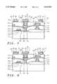
- FIG. 1is a cross sectional representation of the VLSI circuit showing the base dielectric layer, the first electrode pattern formed in the first metal layer, and first thin oxide envelope layer.
- FIG. 2is a cross sectional representation of the VLSI circuit showing the first layer of inter-metal dielectric and second thin envelope oxide layer.
- FIG. 3is a cross sectional representation of the VLSI circuit showing the first inter-level vias.
- FIG. 4is a cross sectional representation of the VLSI circuit showing the thin envelope oxide spacer formed on the sidewalls of the first inter-level vias.
- FIG. 5is a cross sectional representation of the VLSI circuit showing the first inter-level vias filled with the first inter-level metal studs.
- FIG. 6is a cross sectional representation of the VLSI circuit showing the second electrode metal layer and the third thin envelope oxide layer.
- FIG. 7is a cross sectional representation of the VLSI circuit showing the second electrode pattern formed in the second electrode metal layer, the second thin envelope oxide layer and the third thin envelope oxide layer.
- FIG. 8is a cross sectional representation of the VLSI circuit showing the thin envelope oxide spacers formed on the sidewalls of the second electrode pattern.
- FIG. 9is a cross sectional representation of the VLSI circuit showing the second layer of inter-metal dielectric and fourth thin envelope oxide layer.
- FIG. 11is a cross sectional representation of the VLSI circuit showing four patterned layers of electrode metal separated by an air dielectric and a passivation layer over the structure.
- FIG. 1shows a cross sectional representation of a silicon VLSI circuit substrate 20 with doped source/drain regions 28, gate dielectric 23, polysilicon conductors 24, a field oxide isolation region 22, contact studs 26 between the VLSI circuits and the first electrode metal layer, and a base dielectric layer 30 of a material such as borophosphosilicate glass.
- a patterned first electrode metal layer 40is formed on the base dielectric layer using a metal such as aluminum, aluminum alloy, tungsten, copper, or silver deposited using physical vapor deposition or chemical vapor deposition methods and patterned using standard lithographic techniques.
- the contact studs 26 and the first electrode metal layer 40can be formed in one deposition step or sequentially.
- a first thin envelope oxide layer 42 of SiO 2 with a thickness of between about 1000 and 2000 Angstromsis formed over the substrate surface.
- the first thin envelope oxide layeris formed using a chemical vapor deposition with precursor of tetraethoxysilane, or SiH.sub. 4 and O 2 or O 3 .
- tetraethoxysilanewill be referred to as TEOS.
- inter-level vias 35 with sidewalls 27are etched through the first and second thin envelope oxide layers and the first inter-metal dielectric layer using SF 6 , He, CHF 3 , O 2 or the like.
- a thin envelope oxide spacer of SiO 2 with a thickness of between about 1000 and 2000 Angstromsis formed on the sidewalls 27 of the inter-level vias 35.
- the thin envelope oxide spacersare formed by a chemical vapor deposition with TEOS or SiH 4 and O 2 or O 3 over the surface of the substrate followed by vertical anisotropic etching of the SiO 2 using CHF 3 , O 2 , Ar or the like.
- inter-level viasare then filled with inter-level metal studs 29 using metals such as aluminum, aluminum alloy, tungsten, copper, or silver; deposited using physical vapor deposition or chemical vapor deposition methods and patterned using standard lithographic techniques.
- a second metal electrode layer 50is formed over the surface of the substrate using a metal such as aluminum, aluminum alloy, tungsten, copper, or silver deposited using physical vapor deposition or chemical vapor deposition methods with a thickness of between about 4000 and 10,000 Angstroms.
- the inter-level metal studs 29 and the second metal electrode layer 50can be formed in one deposition step or sequentially.
- a third thin envelope oxide layer 42 of SiO 2 with a thickness of between about 1000 and 2000 Angstromsis formed on the surface of the second electrode metal layer using the same method as used for the first and second layers of thin envelope oxide.
- the second electrode pattern 50 having sidewalls 51is formed in the second electrode metal layer and the second and third thin envelope oxide layers using standard lithographic techniques; etching SiO 2 with CHF 3 , O 2 , Ar or the like, and etching Al with Cl 2 , CF 4 , N 2 or the like.
- a thin envelope oxide spacer layeris then formed on the sidewalls 51 of the second electrode pattern using chemical vapor deposition with TEOS or SiH 4 and O 2 or O 3 over the surface of the substrate followed by vertical anisotropic etching of the SiO 2 with CHF 3 , O 2 , Ar or the like.
- FIG. 9shows a second inter-metal dielectric layer 34 and a fourth thin envelope oxide layer 42 formed in preparation for the third electrode metal layer.
- FIG. 10shows the VLSI circuit substrate with four electrode metal layers; 40, 50, 60, and 70; and three inter-metal dielectric layers 34.
- Thin envelope oxide 42surrounds all the electrode metal and inter-level metal studs 29.
- the inter-level dielectricis etched away leaving an air dielectric 85 between the electrode metal layers.
- the inter-level dielectricis etched using a solution with a high etch selectivity for nitride to oxide such as phosphoric acid.
- the surface of all electrode pattern metal and inter-level stud metalis covered with a coating of thin envelope oxide.
- the entire structureis then covered with a passivation layer 80 as shown in FIG. 11.
- the passivation layeris an oxide, such as SiO 2 ; a nitride, such as Si 3 N 4 ; or a polyimide and is deposited using chemical vapor deposition or physical vapor deposition such that it has poor step coverage.
- FIG. 11shows a cross sectional representation of a silicon VLSI circuit substrate 20 with doped source/drain regions 28, polysilicon conductors 24, gate dielectric 23, a field oxide isolation region 22, contact studs 26 between the VLSI circuit and the first electrode metal layer, and a base dielectric layer 30 of a material such as borophosphosilicate glass.
- a patterned first electrode metal layer 40is formed on the base dielectric layer using a metal such as aluminum, aluminum alloy, tungsten, copper, or silver. Additional electrode metal layers 50, 60 and 70 are formed as desired, four such layers are shown in FIG. 11, and interconnected by inter-level metal studs 29.
- the inter-level metal studs 29are formed of metals such as aluminum, aluminum alloy, tungsten, copper, or silver.
- the electrode metal and inter-level metal studsare coated with a thin envelope oxide layer 42 of SiO 2 with a thickness of between about 1000 and 2000 Angstroms.
- the entire structureis covered with a passivation layer 80 of an oxide, such as SiO 2 ; a nitride, such as Si 3 N 4 ; or a polyimide having a poor step coverage.
- the electrode metal layersare separated by an air dielectric 85 which reduces parasitic capacitance and improves circuit performance. System stresses are reduced using the air dielectric which improves device reliability.
Landscapes
- Engineering & Computer Science (AREA)
- Physics & Mathematics (AREA)
- Condensed Matter Physics & Semiconductors (AREA)
- General Physics & Mathematics (AREA)
- Computer Hardware Design (AREA)
- Microelectronics & Electronic Packaging (AREA)
- Power Engineering (AREA)
- Manufacturing & Machinery (AREA)
- Internal Circuitry In Semiconductor Integrated Circuit Devices (AREA)
Abstract
Description
1. FIELD OF THE INVENTION
The invention relates to an improved multi-level conductor electrode structure for VLSI circuits and to the method of forming the improved structure. The multi-level conductor electrode structure is formed using an air dielectric between the conductor electrode levels. The conductor electrodes and the interconnecting inter-level metal studs are coated with a thin envelope oxide. The entire structure is covered with a passivation layer having poor step coverage.
2. DESCRIPTION OF THE RELATED ART
The conventional fabrication of multi-level conductor electrode metal structures uses levels of conductor electrode metal and inter-metal dielectric stacked layer by layer until the desired number of conductor levels are formed. In this invention the inter-level dielectric is replaced by air dielectric thereby reducing parasitic capacitance and improving circuit performance. This invention uses a thin envelope oxide coating on all metal electrodes and inter-metal studs.
There are other patents dealing with air gap isolation. U.S. Pat. No. 5,216,537 to Hornbeck shows a method for making air gap isolation in circuit metalization. U.S. Pat. No. 4,169,000 to Riseman, U.S. Pat. No. 4,710,794 to Koshino et al, and U.S. Pat. No. 5,227,658 to Beyer et al show methods for making air gap isolation between segments of the integrated circuit.
It is a principle objective of this invention to provide a multi-level metal electrode structure for Very Large Scale Integration or VLSI circuits where the metal electrodes are separated by an air dielectric. The air dielectric reduces inter electrode parasitic capacitance and relieves the stress in the multilayer metal electrode structure. Device reliability and performance are improved.
It is also a principle objective of this invention to provide a method of forming a multilevel metal electrode structure for VLSI circuits where the metal electrodes are separated by an air dielectric.
In the fabrication of VLSI circuits multi-level metal electrodes and inter-metal dielectric are stacked layer by layer. This results in large parasitic capacitance between electrodes which degrades circuit performance. In addition large stress levels are present in the structure adversely affecting device reliability. In this invention the inter-metal dielectric material is removed after the structure is formed leaving air, with a reduced dielectric constant, as the inter-metal dielectric. The electrode metals and inter-level via studs are protected by a thin oxide envelope which forms a coating on the metals. Further protection is provided by a passivation layer over top of the metal structure after the inter-level dielectric material is removed.
The reduced dielectric constant reduces inter electrode parasitic capacitance and improves circuit performance. Removing the inter-metal dielectric material also relieves the stress in the structure which improves device reliability. In addition the aspect ratio of the metal vias can be reduced making metal deposition easier.
FIG. 1 is a cross sectional representation of the VLSI circuit showing the base dielectric layer, the first electrode pattern formed in the first metal layer, and first thin oxide envelope layer.
FIG. 2 is a cross sectional representation of the VLSI circuit showing the first layer of inter-metal dielectric and second thin envelope oxide layer.
FIG. 3 is a cross sectional representation of the VLSI circuit showing the first inter-level vias.
FIG. 4 is a cross sectional representation of the VLSI circuit showing the thin envelope oxide spacer formed on the sidewalls of the first inter-level vias.
FIG. 5 is a cross sectional representation of the VLSI circuit showing the first inter-level vias filled with the first inter-level metal studs.
FIG. 6 is a cross sectional representation of the VLSI circuit showing the second electrode metal layer and the third thin envelope oxide layer.
FIG. 7 is a cross sectional representation of the VLSI circuit showing the second electrode pattern formed in the second electrode metal layer, the second thin envelope oxide layer and the third thin envelope oxide layer.
FIG. 8 is a cross sectional representation of the VLSI circuit showing the thin envelope oxide spacers formed on the sidewalls of the second electrode pattern.
FIG. 9 is a cross sectional representation of the VLSI circuit showing the second layer of inter-metal dielectric and fourth thin envelope oxide layer.
FIG. 10 is a cross sectional representation of the VLSI circuit showing four patterned layers of electrode metal and three layers of inter-metal dielectric.
FIG. 11 is a cross sectional representation of the VLSI circuit showing four patterned layers of electrode metal separated by an air dielectric and a passivation layer over the structure.
Refer now to FIG. 1 through FIG. 11, there is shown an embodiment of a method of forming a multi-level conductor electrode structure with an air dielectric for VLSI circuits. FIG. 1 shows a cross sectional representation of a siliconVLSI circuit substrate 20 with doped source/drain regions 28, gate dielectric 23,polysilicon conductors 24, a fieldoxide isolation region 22,contact studs 26 between the VLSI circuits and the first electrode metal layer, and a basedielectric layer 30 of a material such as borophosphosilicate glass. A patterned firstelectrode metal layer 40 is formed on the base dielectric layer using a metal such as aluminum, aluminum alloy, tungsten, copper, or silver deposited using physical vapor deposition or chemical vapor deposition methods and patterned using standard lithographic techniques. Thecontact studs 26 and the firstelectrode metal layer 40 can be formed in one deposition step or sequentially. A first thinenvelope oxide layer 42 of SiO2 with a thickness of between about 1000 and 2000 Angstroms is formed over the substrate surface. The first thin envelope oxide layer is formed using a chemical vapor deposition with precursor of tetraethoxysilane, or SiH.sub. 4 and O2 or O3. Hereafter tetraethoxysilane will be referred to as TEOS.
Next, as shown in FIG. 2, a first layer of inter-metal dielectric 34 is deposited over the surface of the substrate. The inter-metal dielectric is Si3 N4 deposited using chemical vapor deposition with a thickness of between about 1000 Angstroms and 8000 Angstroms. Next a second layer ofthin envelope oxide 42 is deposited on the first layer of inter-metal dielectric. The second layer of thin envelope oxide, like the first layer, is SiO2 with a thickness of between about 1000 and 2000 Angstroms formed using chemical vapor deposition with TEOS or SiH4 and O2 or O3. Next, as shown in FIG. 3,inter-level vias 35 withsidewalls 27 are etched through the first and second thin envelope oxide layers and the first inter-metal dielectric layer using SF6, He, CHF3, O2 or the like. Next, as shown in FIG. 4, a thin envelope oxide spacer of SiO2 with a thickness of between about 1000 and 2000 Angstroms is formed on thesidewalls 27 of theinter-level vias 35. The thin envelope oxide spacers are formed by a chemical vapor deposition with TEOS or SiH4 and O2 or O3 over the surface of the substrate followed by vertical anisotropic etching of the SiO2 using CHF3, O2, Ar or the like.
As shown in FIG. 5 the inter-level vias are then filled withinter-level metal studs 29 using metals such as aluminum, aluminum alloy, tungsten, copper, or silver; deposited using physical vapor deposition or chemical vapor deposition methods and patterned using standard lithographic techniques. Next, as shown in FIG. 6, a secondmetal electrode layer 50 is formed over the surface of the substrate using a metal such as aluminum, aluminum alloy, tungsten, copper, or silver deposited using physical vapor deposition or chemical vapor deposition methods with a thickness of between about 4000 and 10,000 Angstroms. Theinter-level metal studs 29 and the secondmetal electrode layer 50 can be formed in one deposition step or sequentially. Next a third thinenvelope oxide layer 42 of SiO2 with a thickness of between about 1000 and 2000 Angstroms is formed on the surface of the second electrode metal layer using the same method as used for the first and second layers of thin envelope oxide.
As shown in FIG. 7, thesecond electrode pattern 50 havingsidewalls 51 is formed in the second electrode metal layer and the second and third thin envelope oxide layers using standard lithographic techniques; etching SiO2 with CHF3, O2, Ar or the like, and etching Al with Cl2, CF4, N2 or the like. As shown in FIG. 8, a thin envelope oxide spacer layer is then formed on thesidewalls 51 of the second electrode pattern using chemical vapor deposition with TEOS or SiH4 and O2 or O3 over the surface of the substrate followed by vertical anisotropic etching of the SiO2 with CHF3, O2, Ar or the like.
Next additional patterned electrode metal layers and inter-metal dielectric layers are added as desired using the same process steps used to add the second electrode metal layer to the first electrode metal layer. FIG. 9 shows a second inter-metaldielectric layer 34 and a fourth thinenvelope oxide layer 42 formed in preparation for the third electrode metal layer.
FIG. 10 shows the VLSI circuit substrate with four electrode metal layers; 40, 50, 60, and 70; and three inter-metal dielectric layers 34.Thin envelope oxide 42 surrounds all the electrode metal andinter-level metal studs 29. Next, as shown in FIG. 11, the inter-level dielectric is etched away leaving anair dielectric 85 between the electrode metal layers. The inter-level dielectric is etched using a solution with a high etch selectivity for nitride to oxide such as phosphoric acid. The surface of all electrode pattern metal and inter-level stud metal is covered with a coating of thin envelope oxide. The entire structure is then covered with apassivation layer 80 as shown in FIG. 11. The passivation layer is an oxide, such as SiO2 ; a nitride, such as Si3 N4 ; or a polyimide and is deposited using chemical vapor deposition or physical vapor deposition such that it has poor step coverage.
Refer again to FIG. 11, there is shown an embodiment of the multi-level conductor electrode structure with an air dielectric for VLSI circuits. FIG. 11 shows a cross sectional representation of a siliconVLSI circuit substrate 20 with doped source/drain regions 28,polysilicon conductors 24,gate dielectric 23, a fieldoxide isolation region 22,contact studs 26 between the VLSI circuit and the first electrode metal layer, and abase dielectric layer 30 of a material such as borophosphosilicate glass. A patterned firstelectrode metal layer 40 is formed on the base dielectric layer using a metal such as aluminum, aluminum alloy, tungsten, copper, or silver. Additionalelectrode metal layers inter-level metal studs 29. Theinter-level metal studs 29 are formed of metals such as aluminum, aluminum alloy, tungsten, copper, or silver. The electrode metal and inter-level metal studs are coated with a thinenvelope oxide layer 42 of SiO2 with a thickness of between about 1000 and 2000 Angstroms. The entire structure is covered with apassivation layer 80 of an oxide, such as SiO2 ; a nitride, such as Si3 N4 ; or a polyimide having a poor step coverage. The electrode metal layers are separated by anair dielectric 85 which reduces parasitic capacitance and improves circuit performance. System stresses are reduced using the air dielectric which improves device reliability.
While the invention has been particularly shown and described with reference to the preferred embodiments thereof, it will be understood by those skilled in the art that various changes in form and details may be made without departing from the spirit and scope of the invention.
Claims (12)
1. A method of forming a multi-level conductor structure for VLSI circuits, comprising the steps of:
providing a silicon substrate with circuits formed therein, a base dielectric layer formed on said substrate, and contact studs formed in said base dielectric layer making electrical contact with said circuits;
forming a first electrode metal layer on said base dielectric layer and contact studs;
etching a first electrode pattern in said first electrode metal layer;
forming a first thin envelope oxide layer on said first electrode pattern and said base dielectric layer;
forming a first inter-metal dielectric layer over said thin envelope oxide layer;
forming a second thin envelope oxide layer over said first inter-metal dielectric layer;
etching first inter-level vias with sidewalls in said first inter-metal dielectric layer, said first thin envelope oxide layer, and said second thin envelope oxide layer;
forming a thin envelope oxide spacer on said sidewalls of said first inter-level vias;
filling said first inter-level vias with first inter-level metal studs;
forming a second electrode metal layer on said second thin envelope oxide layer and said first inter-level metal studs;
forming a third thin envelope oxide layer on said second electrode metal layer;
etching a second electrode pattern in said second electrode metal layer, said second envelope oxide layer, and said third envelope oxide layer said second electrode pattern having sidewalls;
forming a thin envelope oxide spacer on said sidewalls of said second electrode pattern;
removing all said inter-metal dielectric; and
forming a passivation layer with poor step coverage over said silicon substrate.
2. The method of claim 1, further comprising; after forming said thin envelope oxide spacer on said sidewalls of said second electrode pattern, before removing all said inter-metal dielectric, and before forming said passivation layer with poor step coverage; the steps of:
forming a second layer of inter-metal dielectric over said second electrode pattern in said second electrode metal layer;
forming a fourth thin envelope oxide layer over said second inter-metal dielectric layer;
etching second inter-level vias with sidewalls in said second layer of inter-metal dielectric, said third thin envelope oxide layer, and said fourth thin envelope oxide layer;
forming a thin envelope oxide spacer on said sidewalls of said second inter-level vias;
filling said second inter-level vias with second inter-level metal studs;
forming a third electrode metal layer on said fourth thin envelope oxide layer and said second inter-level metal studs;
forming a fifth thin envelope oxide layer on said third electrode metal layer;
etching a third electrode pattern in said third electrode metal layer, said fourth envelope oxide layer, and said fifth envelope oxide layer said pattern having sidewalls; and
forming a thin envelope oxide spacer on said sidewalls of said third electrode pattern.
3. The method of claim 2, further comprising; after forming said thin envelope oxide spacer on said sidewalls of said third electrode pattern, before removing all said inter-metal dielectric, and before forming said passivation layer with poor step coverage; the steps of:
forming a third layer of inter-metal dielectric over said third electrode pattern in said third electrode metal layer;
forming a sixth thin envelope oxide layer over said third inter-metal dielectric layer;
etching third inter-level vias with sidewalls in said third layer of inter-metal dielectric, said fifth thin envelope oxide layer, and said sixth thin envelope oxide layer;
forming a thin envelope oxide spacer on said sidewalls of said third inter-level vias;
filling said third inter-level vias with third inter-level metal studs;
forming a fourth electrode metal layer on said sixth thin envelope oxide layer and said third inter-level metal studs;
forming a seventh thin envelope oxide layer on said fourth electrode metal layer;
etching a fourth electrode pattern in said fourth electrode metal layer, said sixth envelope oxide layer, and said seventh envelope oxide layer said pattern having sidewalls; and
forming a thin envelope oxide spacer on said sidewalls of said fourth electrode pattern.
4. The method of claim 1 wherein said thin envelope oxide layers are SiO2 with a thickness of between about 1000 and 2000 Angstroms and are formed using chemical vapor deposition with tetraethoxysilane (TEOS) or SiH4 and O2 or O3 as precursors.
5. The method of claim 1 wherein said thin envelope oxide spacers are formed by depositing a layer of SiO2 with a thickness of between about 1000 and 2000 Angstroms using chemical vapor deposition with tetraethoxysilane (TEOS) or SiH4 and O2 or O3 as precursors and vertically anisotropically etching said layer of SiO2 using CHF3, O2, Ar or the like.
6. The method of claim 1 wherein said inter-metal dielectric is Si3 N4 deposited using chemical vapor deposition.
7. The method of claim 6 wherein said inter-metal dielectric is removed by etching in a solution with a high etch selectivity for nitride to oxide.
8. The method of claim 7 wherein said solution with a high etch selectivity for nitride to oxide is phosphoric acid.
9. The method of claim 1 wherein said electrode metal is aluminum, an alloy of aluminum, tungsten, copper, or silver.
10. The method of claim 1 wherein said inter-level metal studs are aluminum, an alloy of aluminum, tungsten, copper, or silver.
11. The method of claim 1 wherein said base dielectric layer is borophosphosilicate glass.
12. The method of claim 1 wherein said passivation layer with poor step coverage is SiO2, Si3 N4, or polyimide.
Priority Applications (2)
| Application Number | Priority Date | Filing Date | Title |
|---|---|---|---|
| US08/275,268US5413962A (en) | 1994-07-15 | 1994-07-15 | Multi-level conductor process in VLSI fabrication utilizing an air bridge |
| US08/668,518US5828121A (en) | 1994-07-15 | 1996-06-27 | Multi-level conduction structure for VLSI circuits |
Applications Claiming Priority (1)
| Application Number | Priority Date | Filing Date | Title |
|---|---|---|---|
| US08/275,268US5413962A (en) | 1994-07-15 | 1994-07-15 | Multi-level conductor process in VLSI fabrication utilizing an air bridge |
Related Child Applications (1)
| Application Number | Title | Priority Date | Filing Date |
|---|---|---|---|
| US42720995ADivision | 1994-07-15 | 1995-04-24 |
Publications (1)
| Publication Number | Publication Date |
|---|---|
| US5413962Atrue US5413962A (en) | 1995-05-09 |
Family
ID=23051559
Family Applications (2)
| Application Number | Title | Priority Date | Filing Date |
|---|---|---|---|
| US08/275,268Expired - LifetimeUS5413962A (en) | 1994-07-15 | 1994-07-15 | Multi-level conductor process in VLSI fabrication utilizing an air bridge |
| US08/668,518Expired - Fee RelatedUS5828121A (en) | 1994-07-15 | 1996-06-27 | Multi-level conduction structure for VLSI circuits |
Family Applications After (1)
| Application Number | Title | Priority Date | Filing Date |
|---|---|---|---|
| US08/668,518Expired - Fee RelatedUS5828121A (en) | 1994-07-15 | 1996-06-27 | Multi-level conduction structure for VLSI circuits |
Country Status (1)
| Country | Link |
|---|---|
| US (2) | US5413962A (en) |
Cited By (59)
| Publication number | Priority date | Publication date | Assignee | Title |
|---|---|---|---|---|
| US5559055A (en)* | 1994-12-21 | 1996-09-24 | Advanced Micro Devices, Inc. | Method of decreased interlayer dielectric constant in a multilayer interconnect structure to increase device speed performance |
| US5670828A (en)* | 1995-02-21 | 1997-09-23 | Advanced Micro Devices, Inc. | Tunneling technology for reducing intra-conductive layer capacitance |
| US5731223A (en)* | 1996-09-24 | 1998-03-24 | Lsi Logic Corporation | Array of solder pads on an integrated circuit |
| US5776828A (en)* | 1995-10-31 | 1998-07-07 | Micron Technology, Inc. | Reduced RC delay between adjacent substrate wiring lines |
| US5814558A (en)* | 1994-08-31 | 1998-09-29 | Texas Instruments Incorporated | Interconnect capacitance between metal leads |
| US5818111A (en)* | 1997-03-21 | 1998-10-06 | Texas Instruments Incorporated | Low capacitance interconnect structures in integrated circuits using a stack of low dielectric materials |
| US5861653A (en)* | 1995-05-11 | 1999-01-19 | Nec Corporation | Semiconductor device having gaseous isolating layer formed in inter-level insulating layer and process of fabrication thereof |
| US5882963A (en)* | 1994-11-24 | 1999-03-16 | Siemens Aktiengesellschaft | Method of manufacturing semiconductor components |
| US5897374A (en)* | 1995-05-22 | 1999-04-27 | Taiwan Semiconductor Manufacturing Company, Ltd. | Vertical via/contact with undercut dielectric |
| US5900668A (en)* | 1995-11-30 | 1999-05-04 | Advanced Micro Devices, Inc. | Low capacitance interconnection |
| EP0872887A3 (en)* | 1997-04-18 | 1999-05-12 | NEC Corporation | Multilevel interconnection structure having an air gap between interconnects |
| EP0924760A2 (en)* | 1997-12-19 | 1999-06-23 | Texas Instruments Incorporated | Address transition detection circuit |
| US5933704A (en)* | 1997-06-02 | 1999-08-03 | Taiwan Semiconductor Manufacturing Company, Ltd. | Method to reveal the architecture of multilayer interconnectors in integrated circuits |
| US5950102A (en)* | 1997-02-03 | 1999-09-07 | Industrial Technology Research Institute | Method for fabricating air-insulated multilevel metal interconnections for integrated circuits |
| US5966634A (en)* | 1996-03-25 | 1999-10-12 | Kabushiki Kaisha Toshiba | Method of manufacturing semiconductor device having multi-layer wiring structure with diffusion preventing film |
| US5994218A (en)* | 1996-09-30 | 1999-11-30 | Kabushiki Kaisha Toshiba | Method of forming electrical connections for a semiconductor device |
| US5998293A (en)* | 1996-06-05 | 1999-12-07 | Advanced Micro Devcies, Inc. | Multilevel interconnect structure of an integrated circuit having air gaps and pillars separating levels of interconnect |
| US6054769A (en)* | 1997-01-17 | 2000-04-25 | Texas Instruments Incorporated | Low capacitance interconnect structures in integrated circuits having an adhesion and protective overlayer for low dielectric materials |
| US6057224A (en)* | 1996-03-29 | 2000-05-02 | Vlsi Technology, Inc. | Methods for making semiconductor devices having air dielectric interconnect structures |
| WO2000035000A1 (en)* | 1998-12-08 | 2000-06-15 | Cvc Products, Inc. | Ultra high-speed semiconductor integrated circuit interconnect structure and fabrication method using free-space dielectric |
| US6078088A (en)* | 1999-01-05 | 2000-06-20 | Advanced Micro Devices, Inc. | Low dielectric semiconductor device with rigid lined interconnection system |
| US6097092A (en)* | 1998-04-22 | 2000-08-01 | International Business Machines Corporation | Freestanding multilayer IC wiring structure |
| US6160316A (en)* | 1998-03-04 | 2000-12-12 | Advanced Micro Devices, Inc. | Integrated circuit utilizing an air gap to reduce capacitance between adjacent metal linewidths |
| US6184159B1 (en)* | 1998-06-12 | 2001-02-06 | Taiwan Semiconductor Manufacturing Corporation | Interlayer dielectric planarization process |
| KR100279790B1 (en)* | 1995-12-28 | 2001-03-02 | 니시무로 타이죠 | Semiconductor device and manufacturing method |
| US6208015B1 (en) | 1996-06-05 | 2001-03-27 | Advanced Micro Devices, Inc. | Interlevel dielectric with air gaps to lessen capacitive coupling |
| US6218282B1 (en) | 1999-02-18 | 2001-04-17 | Advanced Micro Devices, Inc. | Method of forming low dielectric tungsten lined interconnection system |
| US6228770B1 (en) | 2000-03-21 | 2001-05-08 | Chartered Semiconductor Manufacturing Ltd. | Method to form self-sealing air gaps between metal interconnects |
| US6246118B1 (en) | 1999-02-18 | 2001-06-12 | Advanced Micro Devices, Inc. | Low dielectric semiconductor device with rigid, conductively lined interconnection system |
| US6245658B1 (en) | 1999-02-18 | 2001-06-12 | Advanced Micro Devices, Inc. | Method of forming low dielectric semiconductor device with rigid, metal silicide lined interconnection system |
| US6252290B1 (en) | 1999-10-25 | 2001-06-26 | Chartered Semiconductor Manufacturing Ltd. | Method to form, and structure of, a dual damascene interconnect device |
| US6277705B1 (en)* | 1999-12-20 | 2001-08-21 | United Microelectronics Corp. | Method for fabricating an air-gap with a hard mask |
| US6303486B1 (en)* | 2000-01-28 | 2001-10-16 | Advanced Micro Devices, Inc. | Method of fabricating copper-based semiconductor devices using a sacrificial dielectric layer and an unconstrained copper anneal |
| US6376330B1 (en) | 1996-06-05 | 2002-04-23 | Advanced Micro Devices, Inc. | Dielectric having an air gap formed between closely spaced interconnect lines |
| US20020098677A1 (en)* | 2000-05-31 | 2002-07-25 | Micron Technology, Inc. | Multilevel copper interconnects with low-k dielectrics and air gaps |
| US6429522B2 (en)* | 1998-11-03 | 2002-08-06 | International Business Machines Corporation | Microprocessor having air as a dielectric and encapsulated lines |
| US6492705B1 (en) | 1996-06-04 | 2002-12-10 | Intersil Corporation | Integrated circuit air bridge structures and methods of fabricating same |
| US6667552B1 (en) | 1999-02-18 | 2003-12-23 | Advanced Micro Devices, Inc. | Low dielectric metal silicide lined interconnection system |
| US6674167B1 (en)* | 2000-05-31 | 2004-01-06 | Micron Technology, Inc. | Multilevel copper interconnect with double passivation |
| US20040061230A1 (en)* | 2002-09-30 | 2004-04-01 | James Powers | Method of forming an air gap using etch back of inter layer dielectric (ILD) with self-alignment to metal pattern |
| US6780755B2 (en)* | 1999-11-18 | 2004-08-24 | University Of South Florida | Gas dome dielectric system for ULSI interconnects |
| US20040206308A1 (en)* | 2000-01-18 | 2004-10-21 | Micron Technologies, Inc. | Methods and apparatus for making integrated-circuit wiring from copper, silver, gold, and other metals |
| US20040266167A1 (en)* | 2003-06-26 | 2004-12-30 | Dubin Valery M. | Method and apparatus for an improved air gap interconnect structure |
| US20050009326A1 (en)* | 1996-02-06 | 2005-01-13 | Monte Manning | Integrated circuitry and a semiconductor processing method of forming a series of conductive lines |
| US20050023699A1 (en)* | 2000-01-18 | 2005-02-03 | Micron Technology, Inc. | Selective electroless-plated copper metallization |
| US6853054B2 (en)* | 2001-03-30 | 2005-02-08 | Fujitsu Quantum Devices Limited | High frequency semiconductor device |
| US6875685B1 (en) | 2003-10-24 | 2005-04-05 | International Business Machines Corporation | Method of forming gas dielectric with support structure |
| US20050151256A1 (en)* | 1998-04-22 | 2005-07-14 | Natzle Wesley C. | Freestanding multilayer IC wiring structure |
| US20050272255A1 (en)* | 2004-06-02 | 2005-12-08 | Semiconductor Manufacturing International (Shanghai) Corporation | Method and structure for low k interlayer dielectric layer |
| US20060163689A1 (en)* | 2005-01-12 | 2006-07-27 | Hyeoung-Won Seo | Semiconductor device having reduced die-warpage and method of manufacturing the same |
| US7105420B1 (en)* | 1999-10-07 | 2006-09-12 | Chartered Semiconductor Manufacturing Ltd. | Method to fabricate horizontal air columns underneath metal inductor |
| US7253521B2 (en) | 2000-01-18 | 2007-08-07 | Micron Technology, Inc. | Methods for making integrated-circuit wiring from copper, silver, gold, and other metals |
| US20080166874A1 (en)* | 2007-01-05 | 2008-07-10 | International Business Machines Corporation | Formation of vertical devices by electroplating |
| US8779596B2 (en) | 2000-01-18 | 2014-07-15 | Micron Technology, Inc. | Structures and methods to enhance copper metallization |
| US20160105973A1 (en)* | 2013-09-17 | 2016-04-14 | California Institute Of Technology | Micro-fabricated group electroplating technique |
| US20210125992A1 (en)* | 2017-12-22 | 2021-04-29 | Intel Corporation | Interconnect structures for integrated circuits |
| US20210257290A1 (en)* | 2020-02-19 | 2021-08-19 | Nanya Technology Corporation | Semiconductor device with connecting structure and method for fabricating the same |
| US20220084989A1 (en)* | 2020-03-05 | 2022-03-17 | Nanya Technology Corporation | Method for fabricating semiconductor device with connecting structure |
| US20230163209A1 (en)* | 2015-09-29 | 2023-05-25 | Infineon Technologies Austria Ag | Water and ion barrier for iii-v semiconductor devices |
Families Citing this family (18)
| Publication number | Priority date | Publication date | Assignee | Title |
|---|---|---|---|---|
| US5904565A (en)* | 1997-07-17 | 1999-05-18 | Sharp Microelectronics Technology, Inc. | Low resistance contact between integrated circuit metal levels and method for same |
| US6004870A (en)* | 1997-08-26 | 1999-12-21 | Texas Instruments Incorporated | Method for forming a self-aligned contact |
| JP3109478B2 (en)* | 1998-05-27 | 2000-11-13 | 日本電気株式会社 | Semiconductor device |
| US6268276B1 (en)* | 1998-12-21 | 2001-07-31 | Chartered Semiconductor Manufacturing Ltd. | Area array air gap structure for intermetal dielectric application |
| US6150232A (en)* | 1999-02-05 | 2000-11-21 | Chartered Semiconductor Manufacturing Ltd. | Formation of low k dielectric |
| DE19906291A1 (en)* | 1999-02-15 | 2000-08-24 | Siemens Ag | Semiconductor structure, especially a word line structure for memory circuit MOS transistor programming, comprises a conductor line separated from a substrate insulating layer by a cavity and enclosed by an insulating cover |
| US6556962B1 (en) | 1999-07-02 | 2003-04-29 | Intel Corporation | Method for reducing network costs and its application to domino circuits |
| US6596624B1 (en) | 1999-07-31 | 2003-07-22 | International Business Machines Corporation | Process for making low dielectric constant hollow chip structures by removing sacrificial dielectric material after the chip is joined to a chip carrier |
| US6255712B1 (en) | 1999-08-14 | 2001-07-03 | International Business Machines Corporation | Semi-sacrificial diamond for air dielectric formation |
| US6730571B1 (en) | 1999-10-14 | 2004-05-04 | Chartered Semiconductor Manufacturing Ltd. | Method to form a cross network of air gaps within IMD layer |
| US6356031B1 (en) | 2000-05-03 | 2002-03-12 | Time Warner Entertainment Co, Lp | Electroluminescent plastic devices with an integral thin film solar cell |
| US6984892B2 (en)* | 2001-03-28 | 2006-01-10 | Lam Research Corporation | Semiconductor structure implementing low-K dielectric materials and supporting stubs |
| DE10127934A1 (en)* | 2001-06-08 | 2002-12-19 | Infineon Technologies Ag | Strip conductor arrangement used in integrated circuits comprises first insulating layer, second insulating layer, third insulating layer, strip conductors, electrical contact electrically coupling strip conductors in first and third layers |
| US6815358B2 (en) | 2001-09-06 | 2004-11-09 | Seagate Technology Llc | Electron beam lithography method for plating sub-100 nm trenches |
| US6890828B2 (en) | 2003-06-05 | 2005-05-10 | International Business Machines Corporation | Method for supporting a bond pad in a multilevel interconnect structure and support structure formed thereby |
| US20060223332A1 (en)* | 2005-03-30 | 2006-10-05 | Hynix Semiconductor Inc. | Method of manufacturing semiconductor device |
| US7675670B2 (en)* | 2005-10-28 | 2010-03-09 | Miradia Inc. | Fabrication of a high fill ratio silicon spatial light modulator |
| US7453624B2 (en)* | 2005-10-28 | 2008-11-18 | Miradia Inc. | Projection display system including a high fill ratio silicon spatial light modulator |
Citations (11)
| Publication number | Priority date | Publication date | Assignee | Title |
|---|---|---|---|---|
| US4169000A (en)* | 1976-09-02 | 1979-09-25 | International Business Machines Corporation | Method of forming an integrated circuit structure with fully-enclosed air isolation |
| US4710794A (en)* | 1985-02-13 | 1987-12-01 | Kabushiki Kaisha Toshiba | Composite semiconductor device |
| JPS62299051A (en)* | 1986-06-18 | 1987-12-26 | Mitsubishi Electric Corp | Formation of electrode of semiconductor device |
| US4754316A (en)* | 1982-06-03 | 1988-06-28 | Texas Instruments Incorporated | Solid state interconnection system for three dimensional integrated circuit structures |
| US5000818A (en)* | 1989-08-14 | 1991-03-19 | Fairchild Semiconductor Corporation | Method of fabricating a high performance interconnect system for an integrated circuit |
| JPH04320049A (en)* | 1991-04-18 | 1992-11-10 | Fujitsu Ltd | Multilayer wiring structure and its manufacturing method |
| JPH0521617A (en)* | 1991-07-12 | 1993-01-29 | Fujitsu Ltd | Method for manufacturing semiconductor device |
| US5216537A (en)* | 1990-06-29 | 1993-06-01 | Texas Instruments Incorporated | Architecture and process for integrating DMD with control circuit substrates |
| US5227658A (en)* | 1991-10-23 | 1993-07-13 | International Business Machines Corporation | Buried air dielectric isolation of silicon islands |
| US5310700A (en)* | 1993-03-26 | 1994-05-10 | Integrated Device Technology, Inc. | Conductor capacitance reduction in integrated circuits |
| US5324683A (en)* | 1993-06-02 | 1994-06-28 | Motorola, Inc. | Method of forming a semiconductor structure having an air region |
Family Cites Families (7)
| Publication number | Priority date | Publication date | Assignee | Title |
|---|---|---|---|---|
| US3844831A (en)* | 1972-10-27 | 1974-10-29 | Ibm | Forming a compact multilevel interconnection metallurgy system for semi-conductor devices |
| JPS57126147A (en)* | 1981-01-28 | 1982-08-05 | Fujitsu Ltd | Manufacture of semiconductor device |
| US4807016A (en)* | 1985-07-15 | 1989-02-21 | Texas Instruments Incorporated | Dry etch of phosphosilicate glass with selectivity to undoped oxide |
| JP2705111B2 (en)* | 1988-06-10 | 1998-01-26 | 日本電気株式会社 | Method for manufacturing multilayer wiring structure of semiconductor integrated circuit |
| JPH02254722A (en)* | 1989-03-28 | 1990-10-15 | Matsushita Electric Works Ltd | Semiconductor device |
| JPH0395970A (en)* | 1989-09-07 | 1991-04-22 | Ricoh Co Ltd | Polycrystalline silicon thin-film transistor |
| US5391517A (en)* | 1993-09-13 | 1995-02-21 | Motorola Inc. | Process for forming copper interconnect structure |
- 1994
- 1994-07-15USUS08/275,268patent/US5413962A/ennot_activeExpired - Lifetime
- 1996
- 1996-06-27USUS08/668,518patent/US5828121A/ennot_activeExpired - Fee Related
Patent Citations (11)
| Publication number | Priority date | Publication date | Assignee | Title |
|---|---|---|---|---|
| US4169000A (en)* | 1976-09-02 | 1979-09-25 | International Business Machines Corporation | Method of forming an integrated circuit structure with fully-enclosed air isolation |
| US4754316A (en)* | 1982-06-03 | 1988-06-28 | Texas Instruments Incorporated | Solid state interconnection system for three dimensional integrated circuit structures |
| US4710794A (en)* | 1985-02-13 | 1987-12-01 | Kabushiki Kaisha Toshiba | Composite semiconductor device |
| JPS62299051A (en)* | 1986-06-18 | 1987-12-26 | Mitsubishi Electric Corp | Formation of electrode of semiconductor device |
| US5000818A (en)* | 1989-08-14 | 1991-03-19 | Fairchild Semiconductor Corporation | Method of fabricating a high performance interconnect system for an integrated circuit |
| US5216537A (en)* | 1990-06-29 | 1993-06-01 | Texas Instruments Incorporated | Architecture and process for integrating DMD with control circuit substrates |
| JPH04320049A (en)* | 1991-04-18 | 1992-11-10 | Fujitsu Ltd | Multilayer wiring structure and its manufacturing method |
| JPH0521617A (en)* | 1991-07-12 | 1993-01-29 | Fujitsu Ltd | Method for manufacturing semiconductor device |
| US5227658A (en)* | 1991-10-23 | 1993-07-13 | International Business Machines Corporation | Buried air dielectric isolation of silicon islands |
| US5310700A (en)* | 1993-03-26 | 1994-05-10 | Integrated Device Technology, Inc. | Conductor capacitance reduction in integrated circuits |
| US5324683A (en)* | 1993-06-02 | 1994-06-28 | Motorola, Inc. | Method of forming a semiconductor structure having an air region |
Cited By (105)
| Publication number | Priority date | Publication date | Assignee | Title |
|---|---|---|---|---|
| US5814558A (en)* | 1994-08-31 | 1998-09-29 | Texas Instruments Incorporated | Interconnect capacitance between metal leads |
| US5882963A (en)* | 1994-11-24 | 1999-03-16 | Siemens Aktiengesellschaft | Method of manufacturing semiconductor components |
| US5559055A (en)* | 1994-12-21 | 1996-09-24 | Advanced Micro Devices, Inc. | Method of decreased interlayer dielectric constant in a multilayer interconnect structure to increase device speed performance |
| US5670828A (en)* | 1995-02-21 | 1997-09-23 | Advanced Micro Devices, Inc. | Tunneling technology for reducing intra-conductive layer capacitance |
| US5843836A (en)* | 1995-02-21 | 1998-12-01 | Advanced Micro Devices, Inc. | Tunneling technology for reducing intra-conductive layer capacitance |
| US5861653A (en)* | 1995-05-11 | 1999-01-19 | Nec Corporation | Semiconductor device having gaseous isolating layer formed in inter-level insulating layer and process of fabrication thereof |
| US5897374A (en)* | 1995-05-22 | 1999-04-27 | Taiwan Semiconductor Manufacturing Company, Ltd. | Vertical via/contact with undercut dielectric |
| US6396119B1 (en) | 1995-10-31 | 2002-05-28 | Micron Technology, Inc. | Reduced RC delay between adjacent substrate wiring lines |
| US5776828A (en)* | 1995-10-31 | 1998-07-07 | Micron Technology, Inc. | Reduced RC delay between adjacent substrate wiring lines |
| US6548883B2 (en) | 1995-10-31 | 2003-04-15 | Micron Technology, Inc. | Reduced RC between adjacent substrate wiring lines |
| US6146985A (en)* | 1995-11-30 | 2000-11-14 | Advanced Micro Devices, Inc. | Low capacitance interconnection |
| US5900668A (en)* | 1995-11-30 | 1999-05-04 | Advanced Micro Devices, Inc. | Low capacitance interconnection |
| US6306753B1 (en) | 1995-12-28 | 2001-10-23 | Kabushiki Kaisha Toshiba | Feasible, gas-dielectric interconnect process |
| US6307265B1 (en) | 1995-12-28 | 2001-10-23 | Kabushiki Kaisha Toshiba | Feasible, gas-dielectric interconnect process |
| KR100279790B1 (en)* | 1995-12-28 | 2001-03-02 | 니시무로 타이죠 | Semiconductor device and manufacturing method |
| US7208836B2 (en)* | 1996-02-06 | 2007-04-24 | Micron Technology, Inc. | Integrated circuitry and a semiconductor processing method of forming a series of conductive lines |
| US7148134B2 (en) | 1996-02-06 | 2006-12-12 | Micron Technology, Inc. | Integrated circuitry and a semiconductor processing method of forming a series of conductive lines |
| US20050009326A1 (en)* | 1996-02-06 | 2005-01-13 | Monte Manning | Integrated circuitry and a semiconductor processing method of forming a series of conductive lines |
| US20050035456A1 (en)* | 1996-02-06 | 2005-02-17 | Micron Technology, Inc. | Integrated circuitry and a semiconductor processing method of forming a series of conductive lines |
| US5966634A (en)* | 1996-03-25 | 1999-10-12 | Kabushiki Kaisha Toshiba | Method of manufacturing semiconductor device having multi-layer wiring structure with diffusion preventing film |
| US6057224A (en)* | 1996-03-29 | 2000-05-02 | Vlsi Technology, Inc. | Methods for making semiconductor devices having air dielectric interconnect structures |
| US6492705B1 (en) | 1996-06-04 | 2002-12-10 | Intersil Corporation | Integrated circuit air bridge structures and methods of fabricating same |
| US6208015B1 (en) | 1996-06-05 | 2001-03-27 | Advanced Micro Devices, Inc. | Interlevel dielectric with air gaps to lessen capacitive coupling |
| US6376330B1 (en) | 1996-06-05 | 2002-04-23 | Advanced Micro Devices, Inc. | Dielectric having an air gap formed between closely spaced interconnect lines |
| US5998293A (en)* | 1996-06-05 | 1999-12-07 | Advanced Micro Devcies, Inc. | Multilevel interconnect structure of an integrated circuit having air gaps and pillars separating levels of interconnect |
| US5731223A (en)* | 1996-09-24 | 1998-03-24 | Lsi Logic Corporation | Array of solder pads on an integrated circuit |
| US5994218A (en)* | 1996-09-30 | 1999-11-30 | Kabushiki Kaisha Toshiba | Method of forming electrical connections for a semiconductor device |
| US6054769A (en)* | 1997-01-17 | 2000-04-25 | Texas Instruments Incorporated | Low capacitance interconnect structures in integrated circuits having an adhesion and protective overlayer for low dielectric materials |
| US5950102A (en)* | 1997-02-03 | 1999-09-07 | Industrial Technology Research Institute | Method for fabricating air-insulated multilevel metal interconnections for integrated circuits |
| US5818111A (en)* | 1997-03-21 | 1998-10-06 | Texas Instruments Incorporated | Low capacitance interconnect structures in integrated circuits using a stack of low dielectric materials |
| US6064118A (en)* | 1997-04-18 | 2000-05-16 | Nec Corporation | Multilevel interconnection structure having an air gap between interconnects |
| EP0872887A3 (en)* | 1997-04-18 | 1999-05-12 | NEC Corporation | Multilevel interconnection structure having an air gap between interconnects |
| US6368939B1 (en)* | 1997-04-18 | 2002-04-09 | Nec Corporation | Multilevel interconnection structure having an air gap between interconnects |
| US5933704A (en)* | 1997-06-02 | 1999-08-03 | Taiwan Semiconductor Manufacturing Company, Ltd. | Method to reveal the architecture of multilayer interconnectors in integrated circuits |
| EP0924760A2 (en)* | 1997-12-19 | 1999-06-23 | Texas Instruments Incorporated | Address transition detection circuit |
| US6160316A (en)* | 1998-03-04 | 2000-12-12 | Advanced Micro Devices, Inc. | Integrated circuit utilizing an air gap to reduce capacitance between adjacent metal linewidths |
| US7211496B1 (en) | 1998-04-22 | 2007-05-01 | International Business Machines Corporation | Freestanding multiplayer IC wiring structure |
| US20050151256A1 (en)* | 1998-04-22 | 2005-07-14 | Natzle Wesley C. | Freestanding multilayer IC wiring structure |
| US6097092A (en)* | 1998-04-22 | 2000-08-01 | International Business Machines Corporation | Freestanding multilayer IC wiring structure |
| US6184159B1 (en)* | 1998-06-12 | 2001-02-06 | Taiwan Semiconductor Manufacturing Corporation | Interlayer dielectric planarization process |
| US6429522B2 (en)* | 1998-11-03 | 2002-08-06 | International Business Machines Corporation | Microprocessor having air as a dielectric and encapsulated lines |
| WO2000035000A1 (en)* | 1998-12-08 | 2000-06-15 | Cvc Products, Inc. | Ultra high-speed semiconductor integrated circuit interconnect structure and fabrication method using free-space dielectric |
| US6078088A (en)* | 1999-01-05 | 2000-06-20 | Advanced Micro Devices, Inc. | Low dielectric semiconductor device with rigid lined interconnection system |
| US6246118B1 (en) | 1999-02-18 | 2001-06-12 | Advanced Micro Devices, Inc. | Low dielectric semiconductor device with rigid, conductively lined interconnection system |
| US6218282B1 (en) | 1999-02-18 | 2001-04-17 | Advanced Micro Devices, Inc. | Method of forming low dielectric tungsten lined interconnection system |
| US6667552B1 (en) | 1999-02-18 | 2003-12-23 | Advanced Micro Devices, Inc. | Low dielectric metal silicide lined interconnection system |
| US6245658B1 (en) | 1999-02-18 | 2001-06-12 | Advanced Micro Devices, Inc. | Method of forming low dielectric semiconductor device with rigid, metal silicide lined interconnection system |
| US20070007623A1 (en)* | 1999-10-07 | 2007-01-11 | Chartered Semiconductor Manufacturing Ltd. | Method to fabricate horizontal air columns underneath metal inductor |
| US7573081B2 (en)* | 1999-10-07 | 2009-08-11 | Chartered Semiconductor Manufacturing Ltd. | Method to fabricate horizontal air columns underneath metal inductor |
| US7105420B1 (en)* | 1999-10-07 | 2006-09-12 | Chartered Semiconductor Manufacturing Ltd. | Method to fabricate horizontal air columns underneath metal inductor |
| US6252290B1 (en) | 1999-10-25 | 2001-06-26 | Chartered Semiconductor Manufacturing Ltd. | Method to form, and structure of, a dual damascene interconnect device |
| US6780755B2 (en)* | 1999-11-18 | 2004-08-24 | University Of South Florida | Gas dome dielectric system for ULSI interconnects |
| US6277705B1 (en)* | 1999-12-20 | 2001-08-21 | United Microelectronics Corp. | Method for fabricating an air-gap with a hard mask |
| US20050023699A1 (en)* | 2000-01-18 | 2005-02-03 | Micron Technology, Inc. | Selective electroless-plated copper metallization |
| US20070085213A1 (en)* | 2000-01-18 | 2007-04-19 | Micron Technology, Inc. | Selective electroless-plated copper metallization |
| US8779596B2 (en) | 2000-01-18 | 2014-07-15 | Micron Technology, Inc. | Structures and methods to enhance copper metallization |
| US7670469B2 (en) | 2000-01-18 | 2010-03-02 | Micron Technology, Inc. | Methods and apparatus for making integrated-circuit wiring from copper, silver, gold, and other metals |
| US7285196B2 (en) | 2000-01-18 | 2007-10-23 | Micron Technology, Inc. | Methods and apparatus for making integrated-circuit wiring from copper, silver, gold, and other metals |
| US7262505B2 (en) | 2000-01-18 | 2007-08-28 | Micron Technology, Inc. | Selective electroless-plated copper metallization |
| US20040206308A1 (en)* | 2000-01-18 | 2004-10-21 | Micron Technologies, Inc. | Methods and apparatus for making integrated-circuit wiring from copper, silver, gold, and other metals |
| US7402516B2 (en) | 2000-01-18 | 2008-07-22 | Micron Technology, Inc. | Method for making integrated circuits |
| US7262130B1 (en) | 2000-01-18 | 2007-08-28 | Micron Technology, Inc. | Methods for making integrated-circuit wiring from copper, silver, gold, and other metals |
| US7253521B2 (en) | 2000-01-18 | 2007-08-07 | Micron Technology, Inc. | Methods for making integrated-circuit wiring from copper, silver, gold, and other metals |
| US7368378B2 (en) | 2000-01-18 | 2008-05-06 | Micron Technology, Inc. | Methods for making integrated-circuit wiring from copper, silver, gold, and other metals |
| US6303486B1 (en)* | 2000-01-28 | 2001-10-16 | Advanced Micro Devices, Inc. | Method of fabricating copper-based semiconductor devices using a sacrificial dielectric layer and an unconstrained copper anneal |
| US6228770B1 (en) | 2000-03-21 | 2001-05-08 | Chartered Semiconductor Manufacturing Ltd. | Method to form self-sealing air gaps between metal interconnects |
| US7091611B2 (en) | 2000-05-31 | 2006-08-15 | Micron Technology, Inc. | Multilevel copper interconnects with low-k dielectrics and air gaps |
| US20040164419A1 (en)* | 2000-05-31 | 2004-08-26 | Micron Technology, Inc. | Multilevel copper interconnects with low-k dielectrics and air gaps |
| US6674167B1 (en)* | 2000-05-31 | 2004-01-06 | Micron Technology, Inc. | Multilevel copper interconnect with double passivation |
| US20020098677A1 (en)* | 2000-05-31 | 2002-07-25 | Micron Technology, Inc. | Multilevel copper interconnects with low-k dielectrics and air gaps |
| US7067421B2 (en) | 2000-05-31 | 2006-06-27 | Micron Technology, Inc. | Multilevel copper interconnect with double passivation |
| US6995470B2 (en) | 2000-05-31 | 2006-02-07 | Micron Technology, Inc. | Multilevel copper interconnects with low-k dielectrics and air gaps |
| US20050112871A1 (en)* | 2000-05-31 | 2005-05-26 | Micron Technology, Inc. | Multilevel copper interconnect with double passivation |
| US6853054B2 (en)* | 2001-03-30 | 2005-02-08 | Fujitsu Quantum Devices Limited | High frequency semiconductor device |
| US7126223B2 (en)* | 2002-09-30 | 2006-10-24 | Intel Corporation | Semiconductor device formed with an air gap using etch back of inter layer dielectric (ILD) |
| US20040061230A1 (en)* | 2002-09-30 | 2004-04-01 | James Powers | Method of forming an air gap using etch back of inter layer dielectric (ILD) with self-alignment to metal pattern |
| US20070284744A1 (en)* | 2003-06-26 | 2007-12-13 | Dubin Valery M | Apparatus for an improved air gap interconnect structure |
| US20080044999A1 (en)* | 2003-06-26 | 2008-02-21 | Dubin Valery M | Method for an improved air gap interconnect structure |
| US20040266167A1 (en)* | 2003-06-26 | 2004-12-30 | Dubin Valery M. | Method and apparatus for an improved air gap interconnect structure |
| US7304388B2 (en)* | 2003-06-26 | 2007-12-04 | Intel Corporation | Method and apparatus for an improved air gap interconnect structure |
| US7629268B2 (en) | 2003-06-26 | 2009-12-08 | Intel Corporation | Method for an improved air gap interconnect structure |
| US7586196B2 (en) | 2003-06-26 | 2009-09-08 | Intel Corporation | Apparatus for an improved air gap interconnect structure |
| US20050087875A1 (en)* | 2003-10-24 | 2005-04-28 | International Business Machines Corporation | Method of forming gas dielectric with support structure |
| US6875685B1 (en) | 2003-10-24 | 2005-04-05 | International Business Machines Corporation | Method of forming gas dielectric with support structure |
| US7807564B2 (en) | 2004-06-02 | 2010-10-05 | Semiconductor Manufacturing International (Shanghai) Corporation | Method and structure for low-k interlayer dielectric layer |
| US7507656B2 (en)* | 2004-06-02 | 2009-03-24 | Semiconductor Manufacturing International (Shanghai) Corporation | Method and structure for low k interlayer dielectric layer |
| US20080274609A1 (en)* | 2004-06-02 | 2008-11-06 | Semiconductor Manufacturing International (Shanghai) Corporation | Method and structure for low-K interlayer dielectric layer |
| US20050272255A1 (en)* | 2004-06-02 | 2005-12-08 | Semiconductor Manufacturing International (Shanghai) Corporation | Method and structure for low k interlayer dielectric layer |
| US7781851B2 (en)* | 2005-01-12 | 2010-08-24 | Samsung Electronics Co., Ltd. | Semiconductor device having reduced die-warpage and method of manufacturing the same |
| US20060163689A1 (en)* | 2005-01-12 | 2006-07-27 | Hyeoung-Won Seo | Semiconductor device having reduced die-warpage and method of manufacturing the same |
| US7608538B2 (en)* | 2007-01-05 | 2009-10-27 | International Business Machines Corporation | Formation of vertical devices by electroplating |
| US20090294989A1 (en)* | 2007-01-05 | 2009-12-03 | International Business Machines Corporation | Formation of vertical devices by electroplating |
| US20080166874A1 (en)* | 2007-01-05 | 2008-07-10 | International Business Machines Corporation | Formation of vertical devices by electroplating |
| US8247905B2 (en) | 2007-01-05 | 2012-08-21 | International Business Machines Corporation | Formation of vertical devices by electroplating |
| US10617011B2 (en)* | 2013-09-17 | 2020-04-07 | California Institute Of Technology | Micro-fabricated group electroplating technique |
| US20160105973A1 (en)* | 2013-09-17 | 2016-04-14 | California Institute Of Technology | Micro-fabricated group electroplating technique |
| US20230163209A1 (en)* | 2015-09-29 | 2023-05-25 | Infineon Technologies Austria Ag | Water and ion barrier for iii-v semiconductor devices |
| US20210125992A1 (en)* | 2017-12-22 | 2021-04-29 | Intel Corporation | Interconnect structures for integrated circuits |
| US20210257290A1 (en)* | 2020-02-19 | 2021-08-19 | Nanya Technology Corporation | Semiconductor device with connecting structure and method for fabricating the same |
| CN113284877A (en)* | 2020-02-19 | 2021-08-20 | 南亚科技股份有限公司 | Semiconductor element with connection structure and preparation method thereof |
| US11935831B2 (en) | 2020-02-19 | 2024-03-19 | Nanya Technology Corporation | Semiconductor device with connecting structure and method for fabricating the same |
| CN113284877B (en)* | 2020-02-19 | 2024-03-29 | 南亚科技股份有限公司 | Semiconductor component with connection structure and preparation method thereof |
| US20220084989A1 (en)* | 2020-03-05 | 2022-03-17 | Nanya Technology Corporation | Method for fabricating semiconductor device with connecting structure |
| US11315903B2 (en)* | 2020-03-05 | 2022-04-26 | Nanya Technology Corporation | Semiconductor device with connecting structure and method for fabricating the same |
| US11527512B2 (en)* | 2020-03-05 | 2022-12-13 | Nanya Technology Corporation | Method for fabricating semiconductor device with connecting structure |
Also Published As
| Publication number | Publication date |
|---|---|
| US5828121A (en) | 1998-10-27 |
Similar Documents
| Publication | Publication Date | Title |
|---|---|---|
| US5413962A (en) | Multi-level conductor process in VLSI fabrication utilizing an air bridge | |
| US5614765A (en) | Self aligned via dual damascene | |
| US6177329B1 (en) | Integrated circuit structures having gas pockets and method for forming integrated circuit structures having gas pockets | |
| US6051882A (en) | Subtractive dual damascene semiconductor device | |
| US5801094A (en) | Dual damascene process | |
| EP0687005B1 (en) | Method of making interconnections on semiconductor devices | |
| US6403461B1 (en) | Method to reduce capacitance between metal lines | |
| EP0680085B1 (en) | Via formation in polymeric materials | |
| US6083824A (en) | Borderless contact | |
| US20020175414A1 (en) | Novel copper metal structure for the reduction of intra-metal capacitance | |
| US5880026A (en) | Method for air gap formation by plasma treatment of aluminum interconnects | |
| JPH10289953A (en) | Method for planarizing intermetal dielectric between multilevel interconnects on integrated circuits | |
| JP2001085519A (en) | Manufacture of wiring structuer of semiconductor element | |
| JP2007221161A (en) | Capacitor used in semiconductor device and manufacturing method thereof | |
| US20030157788A1 (en) | Method of suppressing void formation in a metal line | |
| US5663108A (en) | Optimized metal pillar via process | |
| JPH01503021A (en) | Flattening method for forming through conductors in silicon wafers | |
| US20070275565A1 (en) | Full removal of dual damascene metal level | |
| US8293638B2 (en) | Method of fabricating damascene structures | |
| US20250316496A1 (en) | Film deposition for patterning process | |
| US6218287B1 (en) | Method of fabricating a semiconductor structure | |
| US6952051B1 (en) | Interlevel dielectric structure | |
| WO1991010261A1 (en) | Semiconductor interconnect structure utilizing a polyimide insulator | |
| GB2325083A (en) | A dual damascene process | |
| US6133628A (en) | Metal layer interconnects with improved performance characteristics |
Legal Events
| Date | Code | Title | Description |
|---|---|---|---|
| AS | Assignment | Owner name:UNITED MICROELECTRONICS CORPORATION, TAIWAN Free format text:ASSIGNMENT OF ASSIGNORS INTEREST;ASSIGNORS:LUR, WATER;WU, JIUNN-YUAN;REEL/FRAME:007086/0751 Effective date:19940628 | |
| STCF | Information on status: patent grant | Free format text:PATENTED CASE | |
| FEPP | Fee payment procedure | Free format text:PAYOR NUMBER ASSIGNED (ORIGINAL EVENT CODE: ASPN); ENTITY STATUS OF PATENT OWNER: LARGE ENTITY | |
| FPAY | Fee payment | Year of fee payment:4 | |
| FPAY | Fee payment | Year of fee payment:8 | |
| FPAY | Fee payment | Year of fee payment:12 |