US5412680A - Linear polarization of semiconductor laser - Google Patents
Linear polarization of semiconductor laserDownload PDFInfo
- Publication number
- US5412680A US5412680AUS08/210,526US21052694AUS5412680AUS 5412680 AUS5412680 AUS 5412680AUS 21052694 AUS21052694 AUS 21052694AUS 5412680 AUS5412680 AUS 5412680A
- Authority
- US
- United States
- Prior art keywords
- active region
- laser
- optical radiation
- array
- polarization
- Prior art date
- Legal status (The legal status is an assumption and is not a legal conclusion. Google has not performed a legal analysis and makes no representation as to the accuracy of the status listed.)
- Expired - Lifetime
Links
Images


Classifications
- H—ELECTRICITY
- H01—ELECTRIC ELEMENTS
- H01S—DEVICES USING THE PROCESS OF LIGHT AMPLIFICATION BY STIMULATED EMISSION OF RADIATION [LASER] TO AMPLIFY OR GENERATE LIGHT; DEVICES USING STIMULATED EMISSION OF ELECTROMAGNETIC RADIATION IN WAVE RANGES OTHER THAN OPTICAL
- H01S5/00—Semiconductor lasers
- H01S5/10—Construction or shape of the optical resonator, e.g. extended or external cavity, coupled cavities, bent-guide, varying width, thickness or composition of the active region
- H01S5/18—Surface-emitting [SE] lasers, e.g. having both horizontal and vertical cavities
- H01S5/183—Surface-emitting [SE] lasers, e.g. having both horizontal and vertical cavities having only vertical cavities, e.g. vertical cavity surface-emitting lasers [VCSEL]
- H01S5/18355—Surface-emitting [SE] lasers, e.g. having both horizontal and vertical cavities having only vertical cavities, e.g. vertical cavity surface-emitting lasers [VCSEL] having a defined polarisation
- B—PERFORMING OPERATIONS; TRANSPORTING
- B82—NANOTECHNOLOGY
- B82Y—SPECIFIC USES OR APPLICATIONS OF NANOSTRUCTURES; MEASUREMENT OR ANALYSIS OF NANOSTRUCTURES; MANUFACTURE OR TREATMENT OF NANOSTRUCTURES
- B82Y20/00—Nanooptics, e.g. quantum optics or photonic crystals
- H—ELECTRICITY
- H01—ELECTRIC ELEMENTS
- H01S—DEVICES USING THE PROCESS OF LIGHT AMPLIFICATION BY STIMULATED EMISSION OF RADIATION [LASER] TO AMPLIFY OR GENERATE LIGHT; DEVICES USING STIMULATED EMISSION OF ELECTROMAGNETIC RADIATION IN WAVE RANGES OTHER THAN OPTICAL
- H01S5/00—Semiconductor lasers
- H01S5/10—Construction or shape of the optical resonator, e.g. extended or external cavity, coupled cavities, bent-guide, varying width, thickness or composition of the active region
- H01S5/18—Surface-emitting [SE] lasers, e.g. having both horizontal and vertical cavities
- H01S5/183—Surface-emitting [SE] lasers, e.g. having both horizontal and vertical cavities having only vertical cavities, e.g. vertical cavity surface-emitting lasers [VCSEL]
- H01S5/18308—Surface-emitting [SE] lasers, e.g. having both horizontal and vertical cavities having only vertical cavities, e.g. vertical cavity surface-emitting lasers [VCSEL] having a special structure for lateral current or light confinement
- H01S5/18322—Position of the structure
- H01S5/1833—Position of the structure with more than one structure
- H01S5/18333—Position of the structure with more than one structure only above the active layer
- H—ELECTRICITY
- H01—ELECTRIC ELEMENTS
- H01S—DEVICES USING THE PROCESS OF LIGHT AMPLIFICATION BY STIMULATED EMISSION OF RADIATION [LASER] TO AMPLIFY OR GENERATE LIGHT; DEVICES USING STIMULATED EMISSION OF ELECTROMAGNETIC RADIATION IN WAVE RANGES OTHER THAN OPTICAL
- H01S5/00—Semiconductor lasers
- H01S5/10—Construction or shape of the optical resonator, e.g. extended or external cavity, coupled cavities, bent-guide, varying width, thickness or composition of the active region
- H01S5/18—Surface-emitting [SE] lasers, e.g. having both horizontal and vertical cavities
- H01S5/183—Surface-emitting [SE] lasers, e.g. having both horizontal and vertical cavities having only vertical cavities, e.g. vertical cavity surface-emitting lasers [VCSEL]
- H01S5/18308—Surface-emitting [SE] lasers, e.g. having both horizontal and vertical cavities having only vertical cavities, e.g. vertical cavity surface-emitting lasers [VCSEL] having a special structure for lateral current or light confinement
- H01S5/18338—Non-circular shape of the structure
- H—ELECTRICITY
- H01—ELECTRIC ELEMENTS
- H01S—DEVICES USING THE PROCESS OF LIGHT AMPLIFICATION BY STIMULATED EMISSION OF RADIATION [LASER] TO AMPLIFY OR GENERATE LIGHT; DEVICES USING STIMULATED EMISSION OF ELECTROMAGNETIC RADIATION IN WAVE RANGES OTHER THAN OPTICAL
- H01S5/00—Semiconductor lasers
- H01S5/10—Construction or shape of the optical resonator, e.g. extended or external cavity, coupled cavities, bent-guide, varying width, thickness or composition of the active region
- H01S5/18—Surface-emitting [SE] lasers, e.g. having both horizontal and vertical cavities
- H01S5/183—Surface-emitting [SE] lasers, e.g. having both horizontal and vertical cavities having only vertical cavities, e.g. vertical cavity surface-emitting lasers [VCSEL]
- H01S5/18386—Details of the emission surface for influencing the near- or far-field, e.g. a grating on the surface
- H01S5/18394—Apertures, e.g. defined by the shape of the upper electrode
- H—ELECTRICITY
- H01—ELECTRIC ELEMENTS
- H01S—DEVICES USING THE PROCESS OF LIGHT AMPLIFICATION BY STIMULATED EMISSION OF RADIATION [LASER] TO AMPLIFY OR GENERATE LIGHT; DEVICES USING STIMULATED EMISSION OF ELECTROMAGNETIC RADIATION IN WAVE RANGES OTHER THAN OPTICAL
- H01S5/00—Semiconductor lasers
- H01S5/30—Structure or shape of the active region; Materials used for the active region
- H01S5/34—Structure or shape of the active region; Materials used for the active region comprising quantum well or superlattice structures, e.g. single quantum well [SQW] lasers, multiple quantum well [MQW] lasers or graded index separate confinement heterostructure [GRINSCH] lasers
- H01S5/3403—Structure or shape of the active region; Materials used for the active region comprising quantum well or superlattice structures, e.g. single quantum well [SQW] lasers, multiple quantum well [MQW] lasers or graded index separate confinement heterostructure [GRINSCH] lasers having a strained layer structure in which the strain performs a special function, e.g. general strain effects, strain versus polarisation
- H01S5/3404—Structure or shape of the active region; Materials used for the active region comprising quantum well or superlattice structures, e.g. single quantum well [SQW] lasers, multiple quantum well [MQW] lasers or graded index separate confinement heterostructure [GRINSCH] lasers having a strained layer structure in which the strain performs a special function, e.g. general strain effects, strain versus polarisation influencing the polarisation
- H—ELECTRICITY
- H01—ELECTRIC ELEMENTS
- H01S—DEVICES USING THE PROCESS OF LIGHT AMPLIFICATION BY STIMULATED EMISSION OF RADIATION [LASER] TO AMPLIFY OR GENERATE LIGHT; DEVICES USING STIMULATED EMISSION OF ELECTROMAGNETIC RADIATION IN WAVE RANGES OTHER THAN OPTICAL
- H01S5/00—Semiconductor lasers
- H01S5/40—Arrangement of two or more semiconductor lasers, not provided for in groups H01S5/02 - H01S5/30
- H01S5/42—Arrays of surface emitting lasers
- H01S5/423—Arrays of surface emitting lasers having a vertical cavity
Definitions
- This inventionrelates to semiconductor lasers and, more particularly, relates to vertical cavity surface emitting lasers that emit optical radiation having the fundamental transverse mode and controlled polarizations.
- a typical semiconductor lasercontains an active region disposed between two parallel mirrors which form therebetween an optical cavity.
- the active regionWhen an electrical current is applied, the active region generates optical radiation which is reflected back and forth between the mirrors before it is emitted.
- the applied currentis greater than a threshold current of the laser, the optical radiation in the optical cavity coherently oscillates to form a standing wave. As a result, the laser emits coherent optical radiation.
- the optical radiation emitted from the lasermay have different spatial distributions. If a laser emits optical radiation that contains only the fundamental transverse mode, the radiation is a narrow laser beam with a Gaussian-distributed cross-section, most intense in the center and less intense at the edges. In contrast, laser radiation having a higher transverse mode displays bright and dark spots across the cross-section of the radiation.
- the transverse modesare conventionally designated as TEM 00 , TEM 01 , TEM 10 , TEM 11 , etc. where TEM 00 is the fundamental transverse mode and the others are higher transverse modes.
- the mirrors that form the optical cavityare parallel to a substrate on which the laser is formed.
- the optical cavity of a VCSELis perpendicular to the substrate; and optical radiation is emitted from the VCSEL in a direction normal to the substrate.
- VCSELshave many advantages over conventional edge emitting lasers. For example, VCSELs can be made extremely small; VCSELs can easily be made into arrays that contain a large number of VCSELs; and VCSELs can be readily integrated monolithically with other semiconductor devices.
- a typical circular shaped VCSEL with a diameter greater than 10 ⁇ memits TEM 00 mode radiation only at low current. At high current, the VCSEL emits higher transverse mode radiation.
- VCSELsemit radiation having uncontrolled directions of polarization.
- applicationse.g. magneto-optical disks
- lasers having controlled directions of polarizationare highly desirable.
- VCSEL arrayscannot be made to emit laser beams, each of which has a predetermined orientation of polarization.
- Adjacent VCSELs in a VCSEL arrayhave a tendency to couple with each other. In some instances, this results in unwanted beam cross sections. It could be prevented if it were possible to control the direction of polarization of adjacent VCSELs since adjacent VCSELs that have perpendicular polarizations usually couple weakly. In other instances, it may be desirable to control the directions of polarization of the VCSELs so that they all have the same direction of polarizations, i.e., have parallel polarizations.
- the active regioncomprises at least one strained semiconductor layer.
- the strained semiconductor layerhas a preferred direction of conductivity which is substantially along a first direction parallel to the mirrors.
- the laseremits optical radiation having a direction of polarization that is substantially parallel to the first direction.
- an elongated active regionis formed between the mirrors.
- the elongated active regionhas longitudinal and transverse axes oriented in directions substantially perpendicular to the direction of optical radiation.
- the dimension of the active region along the transverse axisis sufficiently small so that the laser emits optical radiation having substantially a fundamental transverse mode along the transverse axis.
- the optical radiation emitted from this laserhas a controlled direction of polarization that is substantially parallel to the longitudinal axis.
- a vertical cavity surface emitting laser arraycomprising a plurality of vertical cavity surface emitting lasers integrally formed on a substrate.
- Each of the laserscomprises an elongated active region having longitudinal and transverse axes; and the dimension of the active region along the transverse axis being sufficiently small so that each laser emits optical radiation having substantially a fundamental mode along the transverse axis and a direction of polarization that is substantially parallel to the longitudinal axis.
- each laseremits optical radiation having a direction of polarization that is perpendicular to the direction of polarization of the optical radiation emitted from any adjacent laser.
- FIGS. 1 (a)-(b)illustrate cross-sectional views of a VCSEL that emits linear polarized optical radiation
- FIG. 1 (c)illustrates a top view of a wafer containing the structure of FIGS. 1 (a)-(b);
- FIGS. 2 (a)-(c)depict a top view and longitudinal and transverse cross-sections of a VCSEL that has an elongated active region
- FIGS. 3 (a)-(c)depict a top view and longitudinal and transverse cross-sections of a VCSEL that has an elongated active region and etched trenches;
- FIGS. 4 (a)-(b)depict a top view and a cross-sectional view of a VCSEL that has an elongated active region and implanted regions for suppressing higher mode radiation;
- FIG. 5depicts a top view of a VCSEL that has an elongated active region and a contact layer having a cross-shaped aperture
- FIG. 6depicts a top view of a VCSEL array in which the optical radiation from each VCSEL is linearly polarized in the same direction;
- FIG. 7depicts a top view of a VCSEL array in which the optical radiation from each VCSEL is linearly polarized and is at right angles to that of adjacent VCSELs.
- a VCSELis formed having an active region that contains at least one strained semiconductor layer.
- the strained semiconductor layerdisplays an electrical conduction anisotropy due to the strain and has a preferred direction of electrical conductivity substantially along a first direction.
- the VCSELemits an optical radiation having a direction of polarization that is substantially parallel to the first direction.
- FIG. 1 (a)depicts a cross-section of a preferred embodiment of the invention.
- the VCSELcomprises a GaAs substrate 10 which has a crystal orientation conventionally designated as (100), a first mirror 15, a first spacer 20, an active region 25, a second spacer 30, and a second mirror 35.
- the active regionincludes at least one quantum well.
- the quantum wellcomprises a first semiconductor layer interposed between second and third semiconductor layers. Normally, the second and third semiconductor layers have greater energy bandgaps than the first semiconductor layer.
- FIG. 1 (b)is a more detailed illustration of the cross-section of the active region 25.
- the active regioncomprises three In 0 .2 Ga 0 .8 As layers 22 separated by GaAs layers 21.
- the active regioncontains three In 0 .2 Ga 0 .8 As quantum wells.
- each of GaAs layers 23is about 100 ⁇ thick.
- the outermost GaAs layerscontact AlGaAs spacers 20 and 30.
- the thickness of the In 0 .2 Ga 0 .8 As layersare judiciously chosen in order to maximize the conduction anisotropy that results in a preferred direction of conduction substantially along a first direction.
- the InGaAs quantum wellthere exists tensile strain in the GaAs layers and compressive strain in the InGaAs layers because bulk InGaAs has a greater lattice constant than bulk GaAs. Additionally, the strain in the InGaAs layer increases as the thickness of the InGaAs layer increases.
- the strain in the InGaAs layerproduces an electrical conduction anisotropy which results in a preferred direction of conduction substantially along a conventional crystal lattice direction [110]. Consequently, when an electrical current is applied to the VCSEL, the current prefers to flow along the [110] direction in the active region. As a result, the VCSEL emits optical radiation having a direction of polarization substantially along the crystal direction [110].
- the thickness of the InGaAs layermay be maximized.
- the wavelength of the optical radiation emitted from the VCSELdepends on the composition as well as the thickness of the InGaAs layer.
- changing the thickness of the InGaAs layerchanges the wavelength of the radiation.
- the thickness of the InGaAs layersbecomes greater than a critical thickness, dislocations arise in the InGaAs layers.
- the critical thicknessdepends on the composition of the layers.
- the number of dislocations in the In 0 .2 Ga 0 .8 As layerbecomes substantial when the thickness of the In 0 .2 Ga 0 .8 As layer exceeds approximately 190 ⁇ . If the thickness of each of the In 0 .2 Ga 0 .8 As layers is between approximately 190 ⁇ and 300 ⁇ , dislocations in the In 0 .2 Ga 0 .8 As layers are preferentially formed substantially along the conventional crystal lattice direction [110]. When the thickness of the In 0 .2 Ga 0 .8 As layer exceeds 300 ⁇ , defects along both the [110] and [-110] directions are likely to occur.
- FIG. 1 (c)illustrates a top view of such laser structure epitaxially grown on (100) GaAs substrate 10.
- substrate 10is a commercially available (100) GaAs substrate having a major orientation flat 40. This major orientation flat is parallel to the [110] direction.
- dashed lines 45indicates the preferred direction of conduction in the In 0 .2 Ga 0 .8 As quantum wells.
- a VCSELhas an elongated active region which has longitudinal and transverse axes oriented in directions substantially perpendicular to the direction of the optical radiation emitted from the VCSEL.
- the dimension of the active region along the transverse axisis sufficiently small that the mode of the optical radiation along the transverse axis is the fundamental mode.
- the emitted radiationalso has a controlled direction of polarization that is substantially parallel to the longitudinal axis of the elongated active region.
- FIGS. 2(a)-(c)illustrate a top view, a cross-sectional view along the longitudinal axis A--A' of active region, and a cross-sectional view along the transverse axis B--B' of the active region, respectively, of a preferred embodiment of the VCSEL.
- the VCSELcomprises a substrate 100, a first mirror 105, a first spacer 102, an oval-shaped active region 110, a second spacer 115, and a second mirror 120. Additionally, the VCSEL also includes a current confinement region 125 which laterally surrounds the active region, and an isolation region 130. Two contacts, substrate contact 140 and top contact 135, are also formed.
- oval active region 110has a longitudinal axis 145 and a transverse axis 155.
- the dimensions of the active region along the longitudinal and transverse axesare labelled A and B, respectively.
- transverse dimension Bis less than 6 ⁇ m, so that the transverse mode of optical radiation 165 along the transverse axis is substantially at the fundamental mode.
- the dimension of the active region along the longitudinal axisis approximately 20 ⁇ m.
- Optical radiation 165has a direction of polarization substantially parallel to longitudinal axis 145. This linear polarization is illustratively shown in FIG. 2 (b) as 170.
- mirrors 105 and 120are semiconductor distributed Bragg reflectors comprising a plurality of alternating semiconductor layers of high and low indices of refraction, and each layer is ⁇ /4n thick where ⁇ is the free-space wavelength of the radiation and n is the index of refraction of the layer. If the substrate is an n-type substrate, the first mirror is doped to have an n-type conductivity, and the second mirror is doped to have a p-type conductivity.
- Current confinement region 125is formed by implanting conductivity reducing ions such as Ar, He, H, or O into the region surrounding the active region.
- conductivity reducing ionssuch as Ar, He, H, or O
- an isolation region 130is formed by a deep implantation of one of these ions.
- this VCSELis similar to the fabrication of a conventional VCSEL which is well known to those skilled in the art, and thus is not described in detail here.
- a VCSELin addition to an oval active region 110 lasing., a current confinement region 125, and an isolation region 130, a VCSEL further includes two etched trenches 175 formed at two longitudinal ends of the VCSEL. Each of the trenches vertically extends from the top of the second mirror region through the active region.
- the trencheslimit the current flowing toward the longitudinal ends and, therefore suppress higher transverse mode lasing along the longitudinal direction. Judicious uses of trenches or mesa lead to a conduction anisotropy which is utilized to suppress higher mode lasing.
- the trenchescan also be used for combined "index guiding" and "gain guiding.” Such trenches can be formed by wet chemical etching, reactive-ion etching, or other well-developed etching techniques.
- FIG. 4 (a)illustrates a top-view of another embodiment. Based on the device described in FIG. 2(a)-(c), this VCSEL further includes four implanted regions 180 distributed at the periphery of the active region and symmetrically to both the longitudinal and transverse axes.
- FIG. 4(b)depicts a cross-sectional view of the VCSEL along axis BB' shown in FIG. 4 (a).
- each of the implanted regionsis circularly shaped, and vertically extends from the top of the VCSEL through the active region.
- Implantation regions 180are formed by the implantation of conductivity-reducing ions such as Ar, He, H, or O. The implantation eliminates lasing in these implanted regions, thereby suppressing higher transverse mode lasing along the longitudinal axis.
- the VCSELhas the same structure as the VCSEL shown in FIG. 2(a)-(c) except that contact layer 135 has a cross-shaped aperture having longitudinal and transverse axes.
- the apertureis vertically aligned to the oval active region such that the longitudinal and transverse axes of the aperture are respectively aligned to the longitudinal and transverse axes of the active region.
- the contact layeroverlaps the active region at four locations 151, 152, 153, 154 symmetric to both the longitudinal and transverse axes of the active region.
- this VCSELemits optical radiation having substantially the fundamental transverse mode, i.e. TEM 00 .
- the emitted optical radiationhas a direction of polarization parallel to the longitudinal axis of the active region.
- FIG. 6illustrates a top view of a monolithically integrated VCSEL array.
- each VCSELhas an elongated active region having longitudinal and transverse axes.
- the VCSELsare formed in a way that their longitudinal axes are all substantially parallel to each other.
- each VCSELemits optical radiation that has a direction of polarization 200 parallel to the longitudinal axis of the active region.
- each of the VCSELs from the arrayemits optical radiation having a direction of polarization that is parallel to the polarization of every other VCSEL of the array.
- each of the VCSELs in the array shown in FIG. 6is substantially similar to the VCSELs shown in FIGS. 2 (a)-(c).
- VCSELssuch as those shown in FIG. 3 (a)-(c) or FIGS. 4 (a)-(b) can also be utilized to form the array.
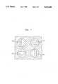
- FIG. 7depicts a top view of another VCSEL array.
- each VCSELemits optical radiation having a direction of polarization 210 or 215 perpendicular to the direction of polarization 215 or 210 of the adjacent VCSELs.
- each of the VCSELs that form the arrayhas an elongated active region.
- the direction of the longitudinal axes of the VCSELsalternates so that the direction of the longitudinal axis of each VCSEL is at right angles to that of its adjacent VCSELs both above and below it and to the left and right in the array.
- the optical radiation emitted from each VCSELhas a direction of polarization along the longitudinal axis of the VCSEL.
- radiation emitted from any VCSELhas a direction of polarization perpendicular to the direction of polarization of its four adjacent VCSELs.
- each of the VCSELsis the same as that depicted in FIGS. 2(a)-(c).
- each of the VCSELscan also be the one shown in FIGS. 4(a)-(b).
Landscapes
- Physics & Mathematics (AREA)
- Optics & Photonics (AREA)
- Chemical & Material Sciences (AREA)
- Engineering & Computer Science (AREA)
- Nanotechnology (AREA)
- Condensed Matter Physics & Semiconductors (AREA)
- General Physics & Mathematics (AREA)
- Electromagnetism (AREA)
- Life Sciences & Earth Sciences (AREA)
- Biophysics (AREA)
- Crystallography & Structural Chemistry (AREA)
- Semiconductor Lasers (AREA)
Abstract
Description
Claims (19)
Priority Applications (1)
| Application Number | Priority Date | Filing Date | Title |
|---|---|---|---|
| US08/210,526US5412680A (en) | 1994-03-18 | 1994-03-18 | Linear polarization of semiconductor laser |
Applications Claiming Priority (1)
| Application Number | Priority Date | Filing Date | Title |
|---|---|---|---|
| US08/210,526US5412680A (en) | 1994-03-18 | 1994-03-18 | Linear polarization of semiconductor laser |
Publications (1)
| Publication Number | Publication Date |
|---|---|
| US5412680Atrue US5412680A (en) | 1995-05-02 |
Family
ID=22783252
Family Applications (1)
| Application Number | Title | Priority Date | Filing Date |
|---|---|---|---|
| US08/210,526Expired - LifetimeUS5412680A (en) | 1994-03-18 | 1994-03-18 | Linear polarization of semiconductor laser |
Country Status (1)
| Country | Link |
|---|---|
| US (1) | US5412680A (en) |
Cited By (69)
| Publication number | Priority date | Publication date | Assignee | Title |
|---|---|---|---|---|
| WO1995031021A1 (en)* | 1994-05-05 | 1995-11-16 | Cornell Research Foundation, Inc. | Strain-compensated multiple quantum well laser structures |
| US5594751A (en)* | 1995-06-26 | 1997-01-14 | Optical Concepts, Inc. | Current-apertured vertical cavity laser |
| EP0760545A1 (en)* | 1995-08-28 | 1997-03-05 | Motorola, Inc. | Short wavelength VSCEL with al-free active region |
| EP0772269A1 (en)* | 1995-10-31 | 1997-05-07 | Hewlett-Packard Company | Vertical-cavity surface-emitting laser |
| US5729567A (en)* | 1995-04-28 | 1998-03-17 | Hewlett-Packard Company | Multilayer film structure and vertical cavity surface emitting lasers |
| US5778018A (en)* | 1994-10-13 | 1998-07-07 | Nec Corporation | VCSELs (vertical-cavity surface emitting lasers) and VCSEL-based devices |
| US5812571A (en)* | 1996-10-25 | 1998-09-22 | W. L. Gore & Associates, Inc. | High-power vertical cavity surface emitting laser cluster |
| WO1998053537A1 (en)* | 1997-05-17 | 1998-11-26 | University Of Bristol | Laser devices |
| US5850408A (en)* | 1994-12-05 | 1998-12-15 | Canon Kabushiki Kaisha | Method of driving semiconductor laser with wide modulation band, optical communication method, semiconductor laser device, node, and optical communication system |
| US5886972A (en)* | 1996-01-03 | 1999-03-23 | Motorola | Recording information in a phase change optical medium with a vertical cavity surface emitting laser |
| EP0924820A3 (en)* | 1997-12-18 | 1999-07-14 | Hewlett-Packard Company | Polarisation-controlled VCSELS using externally applied unitaxial stress |
| US5953362A (en)* | 1997-12-15 | 1999-09-14 | Pamulapati; Jagadeesh | Strain induce control of polarization states in vertical cavity surface emitting lasers and method of making same |
| US5960020A (en)* | 1997-02-20 | 1999-09-28 | Mitsubishi Denki Kabushiki Kaisha | Semiconductor laser diode including ridge and partially disordered active layer |
| US6002705A (en)* | 1997-12-03 | 1999-12-14 | Xerox Corporation | Wavelength and polarization multiplexed vertical cavity surface emitting lasers |
| US6011811A (en)* | 1996-02-27 | 2000-01-04 | Telefonaktiebolaget Lm Ericsson | Buried heterostructure with aluminum-free active layer and method of making same |
| US6134251A (en)* | 1997-07-29 | 2000-10-17 | Seiko Epson Corporation | Surface emission semiconductor laser |
| US6243407B1 (en) | 1997-03-21 | 2001-06-05 | Novalux, Inc. | High power laser devices |
| US6304588B1 (en)* | 1997-02-07 | 2001-10-16 | Xerox Corporation | Method and structure for eliminating polarization instability in laterally-oxidized VCSELs |
| US6310707B1 (en)* | 1996-10-25 | 2001-10-30 | Seiko Epson Corporation | Optical wireless data communication system, and transmitter and receiver used therefor |
| US6399407B1 (en)* | 1996-12-12 | 2002-06-04 | California Institute Of Technology | Methods of electrostatic control in semiconductor devices |
| US20020106160A1 (en)* | 2000-12-29 | 2002-08-08 | Honeywell International Inc. | Resonant reflector for increased wavelength and polarization control |
| WO2002048748A3 (en)* | 2000-08-22 | 2003-03-13 | Univ California | Current leveling layer integrated with aperture for intracavity device |
| US6548835B1 (en) | 2000-11-02 | 2003-04-15 | U-L-M Photonics Gmbh | Optoelectronic device having a highly conductive carrier tunneling current aperture |
| US20030096439A1 (en)* | 1999-09-20 | 2003-05-22 | Hsing-Chung Lee | Methods for forming index guided vertical cavity surface emitting lasers |
| US6570905B1 (en) | 2000-11-02 | 2003-05-27 | U-L-M Photonics Gmbh | Vertical cavity surface emitting laser with reduced parasitic capacitance |
| US6587494B2 (en)* | 1999-12-28 | 2003-07-01 | Kabushiki Kaisha Toshiba | Semiconductor laser device |
| US6683898B2 (en) | 2001-03-09 | 2004-01-27 | Alight Technologies A/S | Mode control using transversal bandgap structure in VCSELs |
| US20040042518A1 (en)* | 2002-09-03 | 2004-03-04 | Tatum James A. | Single mode VCSEL |
| US20040066819A1 (en)* | 2000-11-28 | 2004-04-08 | Johnson Ralph H. | Versatile method and system for single mode VCSELs |
| US20040069208A1 (en)* | 2000-07-14 | 2004-04-15 | Lommen Franciscus Alphons Marie | Process for crystallizing enantiomerically enriched 2-acetylthio-3-phenylpropionic acid |
| US20040081215A1 (en)* | 2002-10-28 | 2004-04-29 | Honeywell International Inc. | Distributed bragg reflector for optoelectronic device |
| US20040101009A1 (en)* | 2002-11-21 | 2004-05-27 | Honeywell International Inc. | Long wavelength VCSEL with tunnel junction, and implant |
| EP1130720A4 (en)* | 1999-09-13 | 2004-07-21 | Furukawa Electric Co Ltd | Surface-emission semiconductor laser |
| US20040222363A1 (en)* | 2003-05-07 | 2004-11-11 | Honeywell International Inc. | Connectorized optical component misalignment detection system |
| US20040247250A1 (en)* | 2003-06-03 | 2004-12-09 | Honeywell International Inc. | Integrated sleeve pluggable package |
| US20040264536A1 (en)* | 2003-06-27 | 2004-12-30 | Honeywell International Inc. | Dielectric VCSEL gain guide |
| US20040264530A1 (en)* | 2003-06-27 | 2004-12-30 | Honeywell International Inc. | VCSEL having thermal management |
| US20040264855A1 (en)* | 2003-06-30 | 2004-12-30 | Bo Su Chen | Optical system with reduced back reflection |
| US20050013542A1 (en)* | 2003-07-16 | 2005-01-20 | Honeywell International Inc. | Coupler having reduction of reflections to light source |
| US20050014390A1 (en)* | 2003-07-18 | 2005-01-20 | Honeywell International Inc. | Edge bead control method and apparatus |
| US20050013539A1 (en)* | 2003-07-17 | 2005-01-20 | Honeywell International Inc. | Optical coupling system |
| US20050013553A1 (en)* | 2003-07-16 | 2005-01-20 | Honeywell International Inc. | Optical coupling system |
| US20050019973A1 (en)* | 2003-07-23 | 2005-01-27 | Palo Alto Research Center, Incorporated | Phase array oxide-confined VCSEL |
| US20050031011A1 (en)* | 2000-11-28 | 2005-02-10 | Biard James R. | Electron affinity engineered VCSELs |
| US20050036533A1 (en)* | 2000-12-29 | 2005-02-17 | Honeywell To Finisar | Tunable detector |
| US6862310B2 (en)* | 2001-01-17 | 2005-03-01 | Avalon Photonics Ltd. | Polarization-stable vertical cavity surface emitting laser device and a method of stabilizing the polarization of a vertical cavity surface emitting laser device |
| US20050092710A1 (en)* | 2003-10-29 | 2005-05-05 | Biard James R. | Long wavelength VCSEL device processing |
| DE19611393B4 (en)* | 1995-03-23 | 2005-07-28 | Samsung Electronics Co., Ltd., Suwon | Vertical cavity resonator surface emitting laser (VCSEL) |
| US20050201680A1 (en)* | 2003-06-30 | 2005-09-15 | Cox James A. | Methods for signal transmission in optical fiber |
| US6963598B1 (en) | 2000-05-23 | 2005-11-08 | Finisar Corporation | System and method for VCSEL polarization control |
| US20060045162A1 (en)* | 2004-08-31 | 2006-03-02 | Finisar Corporation | Distributed bragg reflector for optoelectronic device |
| US20060056762A1 (en)* | 2003-07-02 | 2006-03-16 | Honeywell International Inc. | Lens optical coupler |
| JP2006120881A (en)* | 2004-10-22 | 2006-05-11 | Sony Corp | Surface-emission semiconductor laser element |
| US7054345B2 (en) | 2003-06-27 | 2006-05-30 | Finisar Corporation | Enhanced lateral oxidation |
| US20060268954A1 (en)* | 2004-08-31 | 2006-11-30 | Johnson Ralph H | Light emitting semiconductor device having an electrical confinement barrier near the active region |
| US7298942B2 (en) | 2003-06-06 | 2007-11-20 | Finisar Corporation | Pluggable optical optic system having a lens fiber stop |
| US20080023688A1 (en)* | 2006-07-31 | 2008-01-31 | Finisar Corporation | Efficient carrier injection in a semiconductor device |
| WO2008074927A1 (en)* | 2006-12-21 | 2008-06-26 | Timo Aalto | Vertical cavity surface emitting laser structure |
| US20080232414A1 (en)* | 2007-01-19 | 2008-09-25 | Sony Corporation | Light emitting element, method for manufacturing light emitting element, light emitting element assembly, and method for manufacturing light emitting element assembly |
| US7433381B2 (en) | 2003-06-25 | 2008-10-07 | Finisar Corporation | InP based long wavelength VCSEL |
| US20090305447A1 (en)* | 2008-06-06 | 2009-12-10 | Finisar Corporation | Implanted vertical cavity surface emitting laser |
| US20090310632A1 (en)* | 2008-06-11 | 2009-12-17 | Ricoh Company, Ltd. | Surface emitting laser element, surface emitting laser array, optical scanning device, and image forming apparatus |
| US8031752B1 (en) | 2007-04-16 | 2011-10-04 | Finisar Corporation | VCSEL optimized for high speed data |
| US20150180212A1 (en)* | 2013-12-20 | 2015-06-25 | Seiko Epson Corporation | Vertical cavity surface emitting laser and atomic oscillator |
| US20150180206A1 (en)* | 2013-12-20 | 2015-06-25 | Seiko Epson Corporation | Vertical cavity surface emitting laser and atomic oscillator |
| US20150180214A1 (en)* | 2013-12-20 | 2015-06-25 | Seiko Epson Corporation | Vertical cavity surface emitting laser and atomic oscillator |
| WO2016030741A1 (en)* | 2014-08-27 | 2016-03-03 | Align Technology, Inc. | Illumination means with uniform energy profile and vcsel based low coherence emitter for confocal 3d scanner |
| US20200244040A1 (en)* | 2019-01-27 | 2020-07-30 | Hewlett Packard Enterprise Development Lp | Intensity noise mitigation for vertical-cavity surface emitting lasers |
| WO2023174717A1 (en)* | 2022-03-16 | 2023-09-21 | Trumpf Photonic Components Gmbh | Semiconductor component |
Citations (7)
| Publication number | Priority date | Publication date | Assignee | Title |
|---|---|---|---|---|
| US4949351A (en)* | 1988-04-15 | 1990-08-14 | Omron Tateisi Electronics Co. | Surface-emitting semiconductor laser and manufacturing method of same |
| JPH0311779A (en)* | 1989-06-09 | 1991-01-21 | Hikari Gijutsu Kenkyu Kaihatsu Kk | Manufacture of surface type optical semiconductor element |
| US5063569A (en)* | 1990-12-19 | 1991-11-05 | At&T Bell Laboratories | Vertical-cavity surface-emitting laser with non-epitaxial multilayered dielectric reflectors located on both surfaces |
| US5115442A (en)* | 1990-04-13 | 1992-05-19 | At&T Bell Laboratories | Top-emitting surface emitting laser structures |
| US5245622A (en)* | 1992-05-07 | 1993-09-14 | Bandgap Technology Corporation | Vertical-cavity surface-emitting lasers with intra-cavity structures |
| US5325386A (en)* | 1992-04-21 | 1994-06-28 | Bandgap Technology Corporation | Vertical-cavity surface emitting laser assay display system |
| US5331654A (en)* | 1993-03-05 | 1994-07-19 | Photonics Research Incorporated | Polarized surface-emitting laser |
- 1994
- 1994-03-18USUS08/210,526patent/US5412680A/ennot_activeExpired - Lifetime
Patent Citations (7)
| Publication number | Priority date | Publication date | Assignee | Title |
|---|---|---|---|---|
| US4949351A (en)* | 1988-04-15 | 1990-08-14 | Omron Tateisi Electronics Co. | Surface-emitting semiconductor laser and manufacturing method of same |
| JPH0311779A (en)* | 1989-06-09 | 1991-01-21 | Hikari Gijutsu Kenkyu Kaihatsu Kk | Manufacture of surface type optical semiconductor element |
| US5115442A (en)* | 1990-04-13 | 1992-05-19 | At&T Bell Laboratories | Top-emitting surface emitting laser structures |
| US5063569A (en)* | 1990-12-19 | 1991-11-05 | At&T Bell Laboratories | Vertical-cavity surface-emitting laser with non-epitaxial multilayered dielectric reflectors located on both surfaces |
| US5325386A (en)* | 1992-04-21 | 1994-06-28 | Bandgap Technology Corporation | Vertical-cavity surface emitting laser assay display system |
| US5245622A (en)* | 1992-05-07 | 1993-09-14 | Bandgap Technology Corporation | Vertical-cavity surface-emitting lasers with intra-cavity structures |
| US5331654A (en)* | 1993-03-05 | 1994-07-19 | Photonics Research Incorporated | Polarized surface-emitting laser |
Cited By (119)
| Publication number | Priority date | Publication date | Assignee | Title |
|---|---|---|---|---|
| WO1995031021A1 (en)* | 1994-05-05 | 1995-11-16 | Cornell Research Foundation, Inc. | Strain-compensated multiple quantum well laser structures |
| US5778018A (en)* | 1994-10-13 | 1998-07-07 | Nec Corporation | VCSELs (vertical-cavity surface emitting lasers) and VCSEL-based devices |
| US6154479A (en)* | 1994-10-13 | 2000-11-28 | Nec Corporation | VCSELs (vertical-cavity surface emitting lasers) and VCSEL-based devices |
| US5850408A (en)* | 1994-12-05 | 1998-12-15 | Canon Kabushiki Kaisha | Method of driving semiconductor laser with wide modulation band, optical communication method, semiconductor laser device, node, and optical communication system |
| DE19611393B4 (en)* | 1995-03-23 | 2005-07-28 | Samsung Electronics Co., Ltd., Suwon | Vertical cavity resonator surface emitting laser (VCSEL) |
| US5729567A (en)* | 1995-04-28 | 1998-03-17 | Hewlett-Packard Company | Multilayer film structure and vertical cavity surface emitting lasers |
| US5879961A (en)* | 1995-06-26 | 1999-03-09 | Optical Concepts, Inc. | Method for increasing laser efficiency in a vertical-cavity surface emitting laser |
| US5594751A (en)* | 1995-06-26 | 1997-01-14 | Optical Concepts, Inc. | Current-apertured vertical cavity laser |
| KR100440650B1 (en)* | 1995-08-28 | 2004-10-14 | 모토로라 인코포레이티드 | Surface emitting laser with short wavelength vertical cavity surface |
| EP0760545A1 (en)* | 1995-08-28 | 1997-03-05 | Motorola, Inc. | Short wavelength VSCEL with al-free active region |
| EP0772269A1 (en)* | 1995-10-31 | 1997-05-07 | Hewlett-Packard Company | Vertical-cavity surface-emitting laser |
| US5886972A (en)* | 1996-01-03 | 1999-03-23 | Motorola | Recording information in a phase change optical medium with a vertical cavity surface emitting laser |
| US6011811A (en)* | 1996-02-27 | 2000-01-04 | Telefonaktiebolaget Lm Ericsson | Buried heterostructure with aluminum-free active layer and method of making same |
| US5812571A (en)* | 1996-10-25 | 1998-09-22 | W. L. Gore & Associates, Inc. | High-power vertical cavity surface emitting laser cluster |
| US6310707B1 (en)* | 1996-10-25 | 2001-10-30 | Seiko Epson Corporation | Optical wireless data communication system, and transmitter and receiver used therefor |
| US6399407B1 (en)* | 1996-12-12 | 2002-06-04 | California Institute Of Technology | Methods of electrostatic control in semiconductor devices |
| US7160749B2 (en)* | 1997-02-07 | 2007-01-09 | Xerox Corporation | Method and structure for eliminating polarization instability in laterally—oxidized VCSELs |
| US20060187991A1 (en)* | 1997-02-07 | 2006-08-24 | Xerox Corporation | Laterally oxidized vertical cavity surface emitting lasers |
| US20050158902A1 (en)* | 1997-02-07 | 2005-07-21 | Xerox Corporation | Method and structure for eliminating polarization instability in laterally - oxidized VCSELs |
| US7596161B2 (en) | 1997-02-07 | 2009-09-29 | Xerox Corporation | Laterally oxidized vertical cavity surface emitting lasers |
| US6304588B1 (en)* | 1997-02-07 | 2001-10-16 | Xerox Corporation | Method and structure for eliminating polarization instability in laterally-oxidized VCSELs |
| US5960020A (en)* | 1997-02-20 | 1999-09-28 | Mitsubishi Denki Kabushiki Kaisha | Semiconductor laser diode including ridge and partially disordered active layer |
| US6243407B1 (en) | 1997-03-21 | 2001-06-05 | Novalux, Inc. | High power laser devices |
| US6639931B1 (en) | 1997-05-17 | 2003-10-28 | University Of Bristol | Laser devices |
| WO1998053537A1 (en)* | 1997-05-17 | 1998-11-26 | University Of Bristol | Laser devices |
| US6134251A (en)* | 1997-07-29 | 2000-10-17 | Seiko Epson Corporation | Surface emission semiconductor laser |
| US6603783B1 (en)* | 1997-07-29 | 2003-08-05 | Seiko Epson Corporation | Surface emitting type semiconductor laser |
| US6002705A (en)* | 1997-12-03 | 1999-12-14 | Xerox Corporation | Wavelength and polarization multiplexed vertical cavity surface emitting lasers |
| US5953362A (en)* | 1997-12-15 | 1999-09-14 | Pamulapati; Jagadeesh | Strain induce control of polarization states in vertical cavity surface emitting lasers and method of making same |
| EP0924820A3 (en)* | 1997-12-18 | 1999-07-14 | Hewlett-Packard Company | Polarisation-controlled VCSELS using externally applied unitaxial stress |
| US6188711B1 (en) | 1997-12-18 | 2001-02-13 | Agilent Technologies, Inc. | Polarization-controlled VCSELs using externally applied uniaxial stress |
| EP1130720A4 (en)* | 1999-09-13 | 2004-07-21 | Furukawa Electric Co Ltd | Surface-emission semiconductor laser |
| US20030096439A1 (en)* | 1999-09-20 | 2003-05-22 | Hsing-Chung Lee | Methods for forming index guided vertical cavity surface emitting lasers |
| US6822993B2 (en)* | 1999-09-20 | 2004-11-23 | Jds Uniphase Corporation | Index guided vertical cavity surface emitting lasers |
| US20030138017A1 (en)* | 1999-09-20 | 2003-07-24 | Hsing-Chung Lee | Index guided vertical cavity surface emitting lasers |
| US6577658B1 (en)* | 1999-09-20 | 2003-06-10 | E20 Corporation, Inc. | Method and apparatus for planar index guided vertical cavity surface emitting lasers |
| US6852558B2 (en) | 1999-09-20 | 2005-02-08 | Jds Uniphase Corporation | Methods for forming index guided vertical cavity surface emitting lasers |
| US6687277B2 (en) | 1999-12-28 | 2004-02-03 | Kabushiki Kaisha Toshiba | Semiconductor laser device |
| US6587494B2 (en)* | 1999-12-28 | 2003-07-01 | Kabushiki Kaisha Toshiba | Semiconductor laser device |
| US6963598B1 (en) | 2000-05-23 | 2005-11-08 | Finisar Corporation | System and method for VCSEL polarization control |
| US20040069208A1 (en)* | 2000-07-14 | 2004-04-15 | Lommen Franciscus Alphons Marie | Process for crystallizing enantiomerically enriched 2-acetylthio-3-phenylpropionic acid |
| WO2002048748A3 (en)* | 2000-08-22 | 2003-03-13 | Univ California | Current leveling layer integrated with aperture for intracavity device |
| US6570905B1 (en) | 2000-11-02 | 2003-05-27 | U-L-M Photonics Gmbh | Vertical cavity surface emitting laser with reduced parasitic capacitance |
| US6548835B1 (en) | 2000-11-02 | 2003-04-15 | U-L-M Photonics Gmbh | Optoelectronic device having a highly conductive carrier tunneling current aperture |
| US20050031011A1 (en)* | 2000-11-28 | 2005-02-10 | Biard James R. | Electron affinity engineered VCSELs |
| US7308011B2 (en) | 2000-11-28 | 2007-12-11 | Finisar Corporation | Versatile method and system for single mode VCSELs |
| US7065124B2 (en) | 2000-11-28 | 2006-06-20 | Finlsar Corporation | Electron affinity engineered VCSELs |
| US20040066819A1 (en)* | 2000-11-28 | 2004-04-08 | Johnson Ralph H. | Versatile method and system for single mode VCSELs |
| US20040066820A1 (en)* | 2000-11-28 | 2004-04-08 | Johnson Ralph H. | Versatile method and system for single mode VCSELs |
| US6905900B1 (en) | 2000-11-28 | 2005-06-14 | Finisar Corporation | Versatile method and system for single mode VCSELs |
| US7221691B2 (en) | 2000-11-28 | 2007-05-22 | Finisar Corporation | Versatile method and system for single mode VCSELs |
| US20040213311A1 (en)* | 2000-11-28 | 2004-10-28 | Johnson Ralph H | Single mode vertical cavity surface emitting laser |
| US20050036533A1 (en)* | 2000-12-29 | 2005-02-17 | Honeywell To Finisar | Tunable detector |
| US20020106160A1 (en)* | 2000-12-29 | 2002-08-08 | Honeywell International Inc. | Resonant reflector for increased wavelength and polarization control |
| US6836501B2 (en) | 2000-12-29 | 2004-12-28 | Finisar Corporation | Resonant reflector for increased wavelength and polarization control |
| US8599897B2 (en) | 2000-12-29 | 2013-12-03 | Finisar Corporation | Tunable detector |
| US6862310B2 (en)* | 2001-01-17 | 2005-03-01 | Avalon Photonics Ltd. | Polarization-stable vertical cavity surface emitting laser device and a method of stabilizing the polarization of a vertical cavity surface emitting laser device |
| US6683898B2 (en) | 2001-03-09 | 2004-01-27 | Alight Technologies A/S | Mode control using transversal bandgap structure in VCSELs |
| US6965626B2 (en) | 2002-09-03 | 2005-11-15 | Finisar Corporation | Single mode VCSEL |
| US20040042518A1 (en)* | 2002-09-03 | 2004-03-04 | Tatum James A. | Single mode VCSEL |
| US6990135B2 (en) | 2002-10-28 | 2006-01-24 | Finisar Corporation | Distributed bragg reflector for optoelectronic device |
| US7251264B2 (en) | 2002-10-28 | 2007-07-31 | Finisar Corporation | Distributed bragg reflector for optoelectronic device |
| US20050190812A1 (en)* | 2002-10-28 | 2005-09-01 | Johnson Ralph H. | Distributed bragg reflector for optoelectronic device |
| US20040081215A1 (en)* | 2002-10-28 | 2004-04-29 | Honeywell International Inc. | Distributed bragg reflector for optoelectronic device |
| US20040101009A1 (en)* | 2002-11-21 | 2004-05-27 | Honeywell International Inc. | Long wavelength VCSEL with tunnel junction, and implant |
| US6813293B2 (en) | 2002-11-21 | 2004-11-02 | Finisar Corporation | Long wavelength VCSEL with tunnel junction, and implant |
| US20040222363A1 (en)* | 2003-05-07 | 2004-11-11 | Honeywell International Inc. | Connectorized optical component misalignment detection system |
| US20040247250A1 (en)* | 2003-06-03 | 2004-12-09 | Honeywell International Inc. | Integrated sleeve pluggable package |
| US7298942B2 (en) | 2003-06-06 | 2007-11-20 | Finisar Corporation | Pluggable optical optic system having a lens fiber stop |
| US7433381B2 (en) | 2003-06-25 | 2008-10-07 | Finisar Corporation | InP based long wavelength VCSEL |
| US20040264536A1 (en)* | 2003-06-27 | 2004-12-30 | Honeywell International Inc. | Dielectric VCSEL gain guide |
| US20040264530A1 (en)* | 2003-06-27 | 2004-12-30 | Honeywell International Inc. | VCSEL having thermal management |
| US7054345B2 (en) | 2003-06-27 | 2006-05-30 | Finisar Corporation | Enhanced lateral oxidation |
| US7277461B2 (en) | 2003-06-27 | 2007-10-02 | Finisar Corporation | Dielectric VCSEL gain guide |
| US7075962B2 (en) | 2003-06-27 | 2006-07-11 | Finisar Corporation | VCSEL having thermal management |
| US7149383B2 (en) | 2003-06-30 | 2006-12-12 | Finisar Corporation | Optical system with reduced back reflection |
| US20040264855A1 (en)* | 2003-06-30 | 2004-12-30 | Bo Su Chen | Optical system with reduced back reflection |
| US7139454B2 (en) | 2003-06-30 | 2006-11-21 | Finisar Corporation | Methods for signal transmission in optical fiber |
| US6961489B2 (en) | 2003-06-30 | 2005-11-01 | Finisar Corporation | High speed optical system |
| US20050201680A1 (en)* | 2003-06-30 | 2005-09-15 | Cox James A. | Methods for signal transmission in optical fiber |
| US20060056762A1 (en)* | 2003-07-02 | 2006-03-16 | Honeywell International Inc. | Lens optical coupler |
| US20050013553A1 (en)* | 2003-07-16 | 2005-01-20 | Honeywell International Inc. | Optical coupling system |
| US20050013542A1 (en)* | 2003-07-16 | 2005-01-20 | Honeywell International Inc. | Coupler having reduction of reflections to light source |
| US7210857B2 (en) | 2003-07-16 | 2007-05-01 | Finisar Corporation | Optical coupling system |
| US20050013539A1 (en)* | 2003-07-17 | 2005-01-20 | Honeywell International Inc. | Optical coupling system |
| US6887801B2 (en) | 2003-07-18 | 2005-05-03 | Finisar Corporation | Edge bead control method and apparatus |
| US20050014390A1 (en)* | 2003-07-18 | 2005-01-20 | Honeywell International Inc. | Edge bead control method and apparatus |
| US7257141B2 (en) | 2003-07-23 | 2007-08-14 | Palo Alto Research Center Incorporated | Phase array oxide-confined VCSELs |
| US20050019973A1 (en)* | 2003-07-23 | 2005-01-27 | Palo Alto Research Center, Incorporated | Phase array oxide-confined VCSEL |
| US20050092710A1 (en)* | 2003-10-29 | 2005-05-05 | Biard James R. | Long wavelength VCSEL device processing |
| US7031363B2 (en) | 2003-10-29 | 2006-04-18 | Finisar Corporation | Long wavelength VCSEL device processing |
| US7920612B2 (en) | 2004-08-31 | 2011-04-05 | Finisar Corporation | Light emitting semiconductor device having an electrical confinement barrier near the active region |
| US20060045162A1 (en)* | 2004-08-31 | 2006-03-02 | Finisar Corporation | Distributed bragg reflector for optoelectronic device |
| US7596165B2 (en) | 2004-08-31 | 2009-09-29 | Finisar Corporation | Distributed Bragg Reflector for optoelectronic device |
| US20060268954A1 (en)* | 2004-08-31 | 2006-11-30 | Johnson Ralph H | Light emitting semiconductor device having an electrical confinement barrier near the active region |
| JP2006120881A (en)* | 2004-10-22 | 2006-05-11 | Sony Corp | Surface-emission semiconductor laser element |
| US20080023688A1 (en)* | 2006-07-31 | 2008-01-31 | Finisar Corporation | Efficient carrier injection in a semiconductor device |
| US7829912B2 (en) | 2006-07-31 | 2010-11-09 | Finisar Corporation | Efficient carrier injection in a semiconductor device |
| WO2008074927A1 (en)* | 2006-12-21 | 2008-06-26 | Timo Aalto | Vertical cavity surface emitting laser structure |
| US20100103969A1 (en)* | 2006-12-21 | 2010-04-29 | Timo Aalto | Vertical cavity surface emitting laser structure |
| US20080232414A1 (en)* | 2007-01-19 | 2008-09-25 | Sony Corporation | Light emitting element, method for manufacturing light emitting element, light emitting element assembly, and method for manufacturing light emitting element assembly |
| US8183074B2 (en)* | 2007-01-19 | 2012-05-22 | Sony Corporation | Light emitting element, method for manufacturing light emitting element, light emitting element assembly, and method for manufacturing light emitting element assembly |
| US8031752B1 (en) | 2007-04-16 | 2011-10-04 | Finisar Corporation | VCSEL optimized for high speed data |
| US20090305447A1 (en)* | 2008-06-06 | 2009-12-10 | Finisar Corporation | Implanted vertical cavity surface emitting laser |
| US20090310632A1 (en)* | 2008-06-11 | 2009-12-17 | Ricoh Company, Ltd. | Surface emitting laser element, surface emitting laser array, optical scanning device, and image forming apparatus |
| US7978739B2 (en) | 2008-06-11 | 2011-07-12 | Ricoh Company, Ltd. | Surface emitting laser element, surface emitting laser array, optical scanning device, and image forming apparatus |
| EP2133965A3 (en)* | 2008-06-11 | 2011-02-09 | Ricoh Company, Ltd. | Surface emitting laser element, surface emitting laser array, optical scanning device, and image forming apparatus |
| US20150180212A1 (en)* | 2013-12-20 | 2015-06-25 | Seiko Epson Corporation | Vertical cavity surface emitting laser and atomic oscillator |
| US20150180206A1 (en)* | 2013-12-20 | 2015-06-25 | Seiko Epson Corporation | Vertical cavity surface emitting laser and atomic oscillator |
| US20150180214A1 (en)* | 2013-12-20 | 2015-06-25 | Seiko Epson Corporation | Vertical cavity surface emitting laser and atomic oscillator |
| US9257816B2 (en)* | 2013-12-20 | 2016-02-09 | Seiko Epson Corporation | Vertical cavity surface emitting laser and atomic oscillator |
| WO2016030741A1 (en)* | 2014-08-27 | 2016-03-03 | Align Technology, Inc. | Illumination means with uniform energy profile and vcsel based low coherence emitter for confocal 3d scanner |
| US9660418B2 (en) | 2014-08-27 | 2017-05-23 | Align Technology, Inc. | VCSEL based low coherence emitter for confocal 3D scanner |
| US10148066B2 (en) | 2014-08-27 | 2018-12-04 | Align Technology, Inc. | VCSEL based low coherence emitter for confocal 3D scanner |
| US10756511B2 (en) | 2014-08-27 | 2020-08-25 | Align Technology, Inc. | VCSEL based low coherence emitter for confocal 3D scanner |
| US11387627B2 (en) | 2014-08-27 | 2022-07-12 | Align Technology, Inc. | Intraoral scanner with integrated viewfinder |
| US20200244040A1 (en)* | 2019-01-27 | 2020-07-30 | Hewlett Packard Enterprise Development Lp | Intensity noise mitigation for vertical-cavity surface emitting lasers |
| US10985531B2 (en)* | 2019-01-27 | 2021-04-20 | Hewlett Packard Enterprise Development Lp | Intensity noise mitigation for vertical-cavity surface emitting lasers |
| WO2023174717A1 (en)* | 2022-03-16 | 2023-09-21 | Trumpf Photonic Components Gmbh | Semiconductor component |
Similar Documents
| Publication | Publication Date | Title |
|---|---|---|
| US5412680A (en) | Linear polarization of semiconductor laser | |
| US5056098A (en) | Vertical cavity laser with mirror having controllable reflectivity | |
| US4594718A (en) | Combination index/gain guided semiconductor lasers | |
| US5953362A (en) | Strain induce control of polarization states in vertical cavity surface emitting lasers and method of making same | |
| US6885690B2 (en) | Transverse mode and polarization control of surface emitting lasers through the formation of a dielectric stack | |
| EP0337688B1 (en) | Phase-locked array of semiconductor lasers using closely spaced antiguides | |
| US6040590A (en) | Semiconductor device with electrostatic control | |
| US6683898B2 (en) | Mode control using transversal bandgap structure in VCSELs | |
| EP0333418B1 (en) | Semiconductor laser device | |
| US5363397A (en) | Integrated short cavity laser with bragg mirrors | |
| US7218660B2 (en) | Single-mode vertical cavity surface emitting lasers and methods of making the same | |
| US4821276A (en) | Super-luminescent diode | |
| WO1994021013A1 (en) | Polarized surface-emitting laser | |
| US20050201439A1 (en) | Semiconductor light emitting device and semiconductor light emitting device module | |
| US7570682B2 (en) | VCSEL pumped in a monolithically optical manner and comprising a laterally applied edge emitter | |
| US7164157B2 (en) | Light emitting device and light emitting device module | |
| US6487225B2 (en) | Surface-emitting laser device | |
| US5438585A (en) | Unstable resonator semiconductor laser | |
| US6577661B1 (en) | Semiconductor laser with lateral light confinement by polygonal surface optical grating resonator | |
| US4965806A (en) | Semiconductor laser devices having lateral refractive index tailoring | |
| JPH06196814A (en) | Surface light-emitting device | |
| US4581742A (en) | Semiconductor laser having a non-absorbing passive region with beam guiding | |
| US5586136A (en) | Semiconductor laser device with a misoriented substrate | |
| EP0284684B1 (en) | Inverted channel substrate planar semiconductor laser | |
| JP2927661B2 (en) | Super luminescent diode element and method of manufacturing the same |
Legal Events
| Date | Code | Title | Description |
|---|---|---|---|
| AS | Assignment | Owner name:PHOTONICS RESEARCH INCORPORATED, COLORADO Free format text:ASSIGNMENT OF ASSIGNORS INTEREST;ASSIGNOR:BANDGAP TECHNOLOGY CORPORATION;REEL/FRAME:007101/0102 Effective date:19940706 | |
| AS | Assignment | Owner name:BANDGAP TECHNOLOGY CORPORATION, COLORADO Free format text:ASSIGNMENT OF ASSIGNORS INTEREST;ASSIGNOR:SWIRHUN, STANLEY E.;REEL/FRAME:007213/0576 Effective date:19940321 | |
| AS | Assignment | Owner name:BANDGAP TECHNOLOGY CORPORATION, COLORADO Free format text:ASSIGNMENT OF ASSIGNORS INTEREST;ASSIGNOR:O'NEIL, THOMAS J., JR.;REEL/FRAME:007213/0578 Effective date:19940316 | |
| STCF | Information on status: patent grant | Free format text:PATENTED CASE | |
| AS | Assignment | Owner name:VIXEL CORPORATION, COLORADO Free format text:MERGER;ASSIGNOR:PHOTONICS RESEARCH INCORPORATED;REEL/FRAME:007558/0538 Effective date:19950213 | |
| AS | Assignment | Owner name:ALPERT, HERB, CALIFORNIA Free format text:ASSIGNMENT OF ASSIGNORS INTEREST;ASSIGNOR:VIXEL CORPORATION;REEL/FRAME:007644/0496 Effective date:19950630 Owner name:MOSS, JEROME S., CALIFORNIA Free format text:ASSIGNMENT OF ASSIGNORS INTEREST;ASSIGNOR:VIXEL CORPORATION;REEL/FRAME:007644/0496 Effective date:19950630 | |
| AS | Assignment | Owner name:VIXEL CORPORATION, COLORADO Free format text:RELEASE OF SECURITY INTEREST;ASSIGNORS:ALPERT, HERB;MOSS, JEROME S.;REEL/FRAME:007869/0039 Effective date:19960308 | |
| FPAY | Fee payment | Year of fee payment:4 | |
| AS | Assignment | Owner name:TRANSAMERICA BUSINESS CREDIT CORPORAION, ILLINOIS Free format text:ASSIGNMENT OF ASSIGNORS INTEREST;ASSIGNOR:CIELO COMMUNICATIONS, INC.;REEL/FRAME:009648/0189 Effective date:19981125 Owner name:TRANSAMERICA BUSINESS CREDIT CORPORATION, CALIFORN Free format text:ASSIGNMENT OF ASSIGNORS INTEREST;ASSIGNOR:CIELO COMMUNICATIONS, INC.;REEL/FRAME:009648/0189 Effective date:19981125 | |
| AS | Assignment | Owner name:CIELO COMMUNCATIONS, INC., COLORADO Free format text:ASSIGNMENT OF ASSIGNORS INTEREST;ASSIGNOR:VIXEL CORPORATION;REEL/FRAME:009719/0759 Effective date:19990113 | |
| AS | Assignment | Owner name:CIELO COMMUNICATIONS, INC., COLORADO Free format text:ASSIGNMENT OF ASSIGNORS INTEREST;ASSIGNOR:VIXEL CORPORATION;REEL/FRAME:009711/0202 Effective date:19990113 | |
| AS | Assignment | Owner name:CLELO COMMUNICATIONS, INC., COLORADO Free format text:ASSIGNMENT OF ASSIGNORS INTEREST;ASSIGNOR:VIXEL CORPORATION;REEL/FRAME:009922/0299 Effective date:19990113 | |
| AS | Assignment | Owner name:COMDISCO, INC., ILLINOIS Free format text:SECURITY INTEREST;ASSIGNOR:CIELO COMMUNICATIONS, INC.;REEL/FRAME:013128/0513 Effective date:20020626 | |
| AS | Assignment | Owner name:GATX VENTURES, INC., AS AGENT, CALIFORNIA Free format text:SECURITY AGREEMENT;ASSIGNOR:CIELO COMMUNICATIONS, INC.;REEL/FRAME:013193/0218 Effective date:20020501 | |
| REMI | Maintenance fee reminder mailed | ||
| FPAY | Fee payment | Year of fee payment:8 | |
| SULP | Surcharge for late payment | Year of fee payment:7 | |
| AS | Assignment | Owner name:OPTICAL COMMUNICATION PRODUCTS, INC., CALIFORNIA Free format text:ASSIGNMENT OF ASSIGNORS INTEREST;ASSIGNOR:CIELO COMMUNICTIONS, INC.;REEL/FRAME:013525/0720 Effective date:20021025 | |
| AS | Assignment | Owner name:CIELO COMMUNICATIONS, INC., CALIFORNIA Free format text:RELEASE AND REASSIGNMENT;ASSIGNOR:TRANSAMERICA TECHNOLOGY FINANCE CORPORATION SUCCESSOR IN INTEREST TO TRANSAMERICA BUSINESS CREDIT CORPORATION;REEL/FRAME:013767/0883 Effective date:20021008 | |
| FPAY | Fee payment | Year of fee payment:12 |