US5412646A - Asynchronous transfer mode switch architecture - Google Patents
Asynchronous transfer mode switch architectureDownload PDFInfo
- Publication number
- US5412646A US5412646AUS08/242,217US24221794AUS5412646AUS 5412646 AUS5412646 AUS 5412646AUS 24221794 AUS24221794 AUS 24221794AUS 5412646 AUS5412646 AUS 5412646A
- Authority
- US
- United States
- Prior art keywords
- segments
- concentrator
- inputs
- memories
- cell
- Prior art date
- Legal status (The legal status is an assumption and is not a legal conclusion. Google has not performed a legal analysis and makes no representation as to the accuracy of the status listed.)
- Expired - Lifetime
Links
Images


Classifications
- H—ELECTRICITY
- H04—ELECTRIC COMMUNICATION TECHNIQUE
- H04L—TRANSMISSION OF DIGITAL INFORMATION, e.g. TELEGRAPHIC COMMUNICATION
- H04L12/00—Data switching networks
- H04L12/54—Store-and-forward switching systems
- H04L12/56—Packet switching systems
- H04L12/5601—Transfer mode dependent, e.g. ATM
- H—ELECTRICITY
- H04—ELECTRIC COMMUNICATION TECHNIQUE
- H04L—TRANSMISSION OF DIGITAL INFORMATION, e.g. TELEGRAPHIC COMMUNICATION
- H04L49/00—Packet switching elements
- H04L49/10—Packet switching elements characterised by the switching fabric construction
- H04L49/104—Asynchronous transfer mode [ATM] switching fabrics
- H04L49/105—ATM switching elements
- H04L49/106—ATM switching elements using space switching, e.g. crossbar or matrix
- H—ELECTRICITY
- H04—ELECTRIC COMMUNICATION TECHNIQUE
- H04L—TRANSMISSION OF DIGITAL INFORMATION, e.g. TELEGRAPHIC COMMUNICATION
- H04L49/00—Packet switching elements
- H04L49/15—Interconnection of switching modules
- H04L49/1515—Non-blocking multistage, e.g. Clos
- H04L49/153—ATM switching fabrics having parallel switch planes
- H04L49/1538—Cell slicing
- H—ELECTRICITY
- H04—ELECTRIC COMMUNICATION TECHNIQUE
- H04L—TRANSMISSION OF DIGITAL INFORMATION, e.g. TELEGRAPHIC COMMUNICATION
- H04L49/00—Packet switching elements
- H04L49/25—Routing or path finding in a switch fabric
- H04L49/253—Routing or path finding in a switch fabric using establishment or release of connections between ports
- H04L49/255—Control mechanisms for ATM switching fabrics
- H—ELECTRICITY
- H04—ELECTRIC COMMUNICATION TECHNIQUE
- H04L—TRANSMISSION OF DIGITAL INFORMATION, e.g. TELEGRAPHIC COMMUNICATION
- H04L49/00—Packet switching elements
- H04L49/45—Arrangements for providing or supporting expansion
- H04L49/455—Provisions for supporting expansion in ATM switches
- H—ELECTRICITY
- H04—ELECTRIC COMMUNICATION TECHNIQUE
- H04L—TRANSMISSION OF DIGITAL INFORMATION, e.g. TELEGRAPHIC COMMUNICATION
- H04L12/00—Data switching networks
- H04L12/54—Store-and-forward switching systems
- H04L12/56—Packet switching systems
- H04L12/5601—Transfer mode dependent, e.g. ATM
- H04L2012/5638—Services, e.g. multimedia, GOS, QOS
- H04L2012/5646—Cell characteristics, e.g. loss, delay, jitter, sequence integrity
- H04L2012/565—Sequence integrity
- H—ELECTRICITY
- H04—ELECTRIC COMMUNICATION TECHNIQUE
- H04L—TRANSMISSION OF DIGITAL INFORMATION, e.g. TELEGRAPHIC COMMUNICATION
- H04L12/00—Data switching networks
- H04L12/54—Store-and-forward switching systems
- H04L12/56—Packet switching systems
- H04L12/5601—Transfer mode dependent, e.g. ATM
- H04L2012/5678—Traffic aspects, e.g. arbitration, load balancing, smoothing, buffer management
- H04L2012/5681—Buffer or queue management
Definitions
- the inventionrelates to packet switching systems and more particularly relates to an architecture for an asynchronous transfer mode switch.
- Asynchronous Transfer Mode (ATM) switchhinges on whether the switch is "growable"-meaning that the switching capacity of the switch may be expanded to handle an increase in bandwidth.
- ATMAsynchronous Transfer Mode
- U.S. Pat. No. 5,256,265discloses an architecture for an ATM switch which may grow (expand) from an 8 ⁇ 8 packet switch to a 32 ⁇ 32 packet switch, as shown in FIG. 1.
- One drawback of such an architectureis that when the capacity of the switch is expanded, the required concentration access speed increases proportionately.
- Another drawbackis that the bandwidth data rate at the output of an expansion unit 404 becomes k times the input bandwidth data rate of the switch, where k is the number of 8 ⁇ 8 packet switch modules employed at the output of the switch.
- the expansion bandwidthis kxnxR, where R is the input bandwidth of each line and is typically 2.4 gigabits/sec. Since k is proportional to the size of an ATM switch, i.e., k is proportional to n, then it can be appreciated that the bandwidth of the interconnection between the expansion unit 404 and associated concentrators 101 grows as the square of the size of the switch and, therefore, becomes unwieldy to implement when the size of the ATM switch is increased.
- the interconnection bandwidth between the expansion unit 404 and associated concentrators 101may be readily managed by constructing an ATM switch such that the interconnection is contained within integrated circuit devices, rather than being external to the devices, as is done in the prior art.
- the expansion and concentration functions for the ATM switchare contained, in accord with an aspect of the invention, on the same device.
- the current level of technologydoes not permit integration of the expansion and concentration functions on a single device for a high capacity ATM switch.
- the decrease in concentrator access time that occurs as a result of an increase in the bandwidth (capacity) of an ATM switchmay be readily dealt with, in accordance with an aspect of the invention, by using in each concentrator unit a plurality of parallel First In, First Out (FIFO) memory circuits, rather than just a single memory circuit.
- FIFOFirst In, First Out
- FIG. 1is a broad block diagram of a prior art ATM switch:
- FIG. 2is a broad block diagram of an ATM switch arranged in accord with the principles of the invention
- FIG. 3is a block diagram of the expansion module of FIG. 2;
- FIG. 4is a block diagram of the expand/concentrator unit of FIG. 3;
- FIGS. 5 and 6graphically illustrate the operation of an expand/concentrator unit of FIG. 4;
- FIG. 7is a functional block diagram of the FIFO control unit of FIG. 4;
- FIG. 8illustrates in simplified block diagram form the way in which the ATM switch of FIG. 2 may be expanded to accommodate 2n inputs.
- FIG. 9illustrates in simplified block diagram form the way in which the ATM switch of FIG. 2 may be expanded into a mnxn switch.
- ATM switch 100 shown in FIG. 2comprises an expansion module 200 that receives n inputs, each providing a stream of ATM cells at a predetermined maximum rate of, e.g., 2.4 Gb/s. Each input is interconnected internally to the expansion module 200 (shown below) via a respective one of the routing processors 55-l through 55-n.
- a routing processor 55responsive to receipt of a cell via an associated data path, prepends to the cell header routing information identifying a particular one of the packet switch modules 300-l through 300-k that will forward the cell to its intended destination.
- the routing informationwould identify more than one packet switch module, which would then forward the cell to a number of different destinations.
- the resulting cellis then supplied to the concentrator units contained in expansion module 200.
- the outputs of the concentratorsare then supplied to respective packet switch modules 300-l through 300-k based on the prepended routing information. It is noted that many techniques are known for implementing a packet switch module 300. For example, see U.S. Pat. Nos. 4,603,416, 5,233,606 and 5,278,969 which disclose examples of such packet switch modules.
- Expansion module 200more particularly, includes a plurality of conventional cell multiplexer/cell slicer units 60-l through 60-k, a plurality of expand/concentrator units 70-l through 70-j and a plurality of conventional segment combiner circuits 80-l through 80-k, as shown in FIG. 3.
- Each multiplexer/cell slicer unite.g., unit 60-l, serves n/k inputs such that a stream of data cells may be received via each input.
- a multiplexer/cell slicer unit 60When a cell is received at one of its inputs, a multiplexer/cell slicer unit 60, e.g., unit 60-l, "strips off" the aforementioned prepended routing information and supplies the information to each expand/concentrator unit 70 via an associated one of the multilead busses 10-l through 10-k.
- the leads of multilead bus 10-lrespectively connect to expand/concentrator units 70-l through 70-j.
- unit 60-ldistributes the routing information that it receives to each of the units 70-l through 70-j.
- Each unit 70-l through 70-jthus receives routing information relating to respective cells from each of the units 60-l through 60-k.
- Each multiplexer/cell slicer unit 60also multiplexes the cells that it receives via its associated inputs into a single stream of cells having a bandwidth of Rn/k, where R, as mentioned above, is the bandwidth of each input line, n is the total number of inputs 50 and k is the number of packet switch modules 300.
- Cell multiplier/cell slicer unit 60then segments each multiplexer cell into j segments and supplies the segments to expand/concentrator circuits 70-l through 70-j, respectively. For example, a first segment is supplied to circuit 70-l, a second segment is supplied to circuit 70-2, a third segment is supplied to circuit 70-3 (not shown) and so on.
- This aspectis represented in FIG. 3 by designations 61-l through 61-k, in which a plurality of connections 61-l originate from units 60-l through 60k, respectively.
- CLUsConcentrator Logic Units
- Such fan out of a segmentis, in accord with an aspect of the invention, internal to the expand/concentrator unit 70. (This is in contrast to the prior art in which the fan out is disposed external to a concentrator unit, as shown in FIG. 1, i.e., the expansion between elements 404 and 401.)
- Each CLU of a unit 70, FIG. 3then either accepts and stores or discards the segment that it receives at its input based on the associated routing information received via a lead of a respective one of the control busses 10-l through 10-k.
- Each expand/concentrator 70concentrates the segments that it accepts via respective ones of its k inputs into streams of segments and forwards the streams to respective ones of the segment combiner circuits 80-l through 80-k.
- Each segment combiner circuit 80accepts segments from each of the expand/concentrator units 70 and combines associated segments into an ATM cell. The combiner circuit 80 then forwards the packet to an associated packet switch module 300.
- a switch module 300forwards the cell to a destination identified, directly or indirectly, in the cell header.
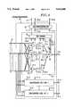
- an expand/concentrator unit 70includes k CLUs as shown in FIG. 4.
- a segment received at a unit 70is fanned out, in accord with an aspect of the invention, to each of the CLUs 72-l through 72-k.
- a CLUe.g., CLU 72-l
- the storage and retrieval of a segment in a FIFO 74is also under the control of circuit 75, as will be discussed below.
- Each FIFO 74is associated with an input of output selector circuit 79, which also operates under the control of FIFO control circuit 75.
- An expand/concentrator unit 70also includes a selection/distribution circuit 25.
- the selection/distribution circuit 25,more particularly, associates routing information that it receives via each of the multi-lead busses 10 with a particular CLU, e.g., CLU 72-l. Circuit 25 then multiplexes the selected information onto respective leads of a multilead bus 11, e.g., bus 11-l, for presentation to the associated FIFO control circuit 75.
- an expand/concentrator unit 70receives routing information associated with a cell via one of the busses 10 and presents such information to its associated selection/distribution circuit 25 for processing and distribution over respective ones of the busses 11.
- selection/distribution circuit 25assembles the routing information contained on busses 10-l through 10-k and then associates the information with cells destined for the same Concentrator Logic Units (CLUs), 72-i by "packing" such information onto the same control bus 11-i for delivery to the associated CLU. For example, the destination addresses for cells received via inputs 50-l through 50-n/k are forwarded over control bus 10-l.
- CLUsConcentrator Logic Units
- selection/distribution 25passes the destination information received (a) via input 50-l and control bus 10-l to control bus 11-l, (b) via inputs 50-2 through 50-n/k and control bus 10-l to control bus 11-3, and (c) via all other inputs and control busses 10-2 through 10-k to control bus 11-l.
- the associated FIFO control circuit 75controls (a) which input of a selector 73 is passed to its associated FIFO 74 via respective ones of busses 76-l through 76-K, and (b) which FIFO 74 will store the inputed segment via respective ones of busses 77-l through 77-k.
- Circuit 75also controls via bus 78 which one of the FIFO's 74-l through 74-K presents a cell segment to a respective input of selector 79, and controls which one of the selection 79 inputs is presented to the associated output 71, during a current system time slot.
- FIFO control circuit 75also operates to ensure that the storage of segments accepted via associated selectors 73 is done, in accord with an aspect of the invention, in round-robin fashion so that the storage of such segments is equally distributed across all of the FIFOs 74-l through 74-k of a CLU. What this means is that when a number of segments are selected by respective ones of the selectors 73, then such segments are supplied, under the control of circuit 75, to associated ones of the FIFOs 74 for storage therein. Circuit 75 thus determines and controls via busses 76 and 77 which segments are stored in which FIFOs 74.
- busses 10selection/distribution 25
- busses 11FIFO control 75
- busses 76, 77 and 78are not shown. It is to be understood, of course, that FIG. 5 and the following discussion is not to be taken as a limitation of our inventive architecture and is provided for the sole purpose of furthering an understanding of our invention.
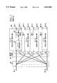
- selectors 73-l through 73-4as shown in FIG. 5 (and as also shown in FIG. 4 for selectors 73-l through 73-k.) Responsive to particular control signals issued by FIFO control 75 (not shown in FIG. 5), selectors 73-l, 73-2 and 73-3 select and output segments A, B and C, respectively.
- FIFO control 75directs FIFOs 74-1, 74-2 and 74-3 to respectively store segments A, B and C in their respective memories, but not segment X 1 , since that segment may be destined for one or more packet switch modules, other than the one connected to bus 71. This will also be the case for segments X 2 and X 3 arriving at time slot T 2 . This is shown in the time diagram of FIG. 6 for time slot T 0 . Assume that during the next time slot T 1 cell segments D, E and F are supplied via respective leads 61 to each of the selectors 73.
- FIFO control 75directs selectors 73-4, 73-1 and 73-2 to select and output segments D, E and F, respectively.
- FIFO control 75directs FIFO 74-4 to store segment D in its memory and directs FIFOs 74-1 and 74-2 to store segments E and F, respectively.
- FIFO control 75directs FIFO 74-1 to output segment A to selector 79 for presentation to lead 71.
- the contents of FIFOs 74-1 through 74-4is shown in FIG.
- time slot T 1which indicates that segment A has been outputted to selector 79 and segments D, E and F have been stored in FIFOs 74-4, 74-1 and 74-2, respectively.
- the timing diagramalso shows that during succeeding time slots T 2 through T 6 segments B through F are respectively outputted in sequence to selector 79 as also shown for lead 71, thus completing the concentrating function of the segments to the same lead.
- FIG. 7A functional block diagram of FIFO control unit 75 is illustrated in FIG. 7.
- the inputs to a unit 75comprises a k-bit bus 11.
- a bit within bus 11is asserted as a "1" if the corresponding input of bus 61 contains a cell segment that is to be accepted and forwarded to an associated Packet Switch Module (PSM).
- PSMPacket Switch Module
- the outputs of a FIFO control unit 75include control busses 76 and 77 as well as control bus 78.
- Each bus 76-iis a k-bit bus that controls which input a corresponding selector 73-i selects.
- Control bus 77is a k-bit but such that each lead 77-i is a 1-bit push control signal that controls whether a cell segment is "pushed" (stored) into the corresponding FIFO 74-i.
- Control bus 78is also a k-bit bus such that each lead 78-i carries a one-bit pop signal that controls if a cell segment is to be "popped" (read) from the corresponding FIFO 74-i.
- Control bus 78also controls which of the FIFO 74 outputs is selected by selector 79 for presentation to bus 71, as mentioned above.
- the POINTER(t)is then set to ((1c+q) modulo k) and t is incremented in preparation for the next cell cycle.
- the push control signal 77-i for the ((1c+i)th FIFOis asserted if one of the leads of bus 76-i is asserted, i.e., the associated selector 73-i is in the process of selecting a cell segment via one of the inputs 61, so that the selected cell segment will be pushed into the corresponding FIFO; otherwise, the push control signal 77-i will be inactive.
- Control bus 78is also updated so that the contents of the next FIFO is selected by selector 79 in round-robin fashion. Specifically, if the ith lead of bus 78 is asserted during time t, then the (i+1) modulo k th lead is asserted during time t+1.
- a breakdown of a FIFO control unit 75functionally would include an active input counter and a plurality (e.g., k) selector controllers 20.
- the active input counterwould include k summing circuits 10 for generating a set of outputs SUM[l ] through SUM[k] such that SUM[j] is indicative of the number of active inputs from input l through input j.
- the value SUM[k]is supplied to modulo k adder 12 so that the value of 1c for the next cycle may be generated, as mentioned above.
- circulating shift register 14includes k register circuits such that a bit is shifted from one register to a next register responsive to a clock signal as a way of activating a corresponding one of the leads of bus 78.
- An input selector controller 20, on the other hand, in a functional sense,would include k comparators 21, k "AND" circuits 22 and a modulo k subtracter 23.
- the modulo k subtractergenerates a distance (i.e., an off-set value) of the ith selector from the last FIFO accessed in cell cycle t-1. For example, if k equals 8 and if the latter FIFO happened to be FIFO 3, then tile off-set value for selector controller 7 (1) would be 4 (6).
- the off-set valuewould then be compared with the set of outputs generated by the active input counter. If a match is found and tile associated active bit equals a value of one, then the corresponding "AND" gate would output a value of one to its associated lead 76. As such, at most only one lead 76 of a selector controller output would be active.
- FIG. 8illustrates the way in which our inventive architecture may be expanded to double the capacity of the switch of FIG. 2.
- each of the n inputsis supplied to expansion modules 200-1 and 200-2 and each of the other n inputs is supplied to expansion modules 200-3 and 200-4.
- the outputs of expansion modules 200-1 and 200-3are combined two at a time via a plurality (e.g., k) 2:1 concentrators 250-l through 250-k, in the manner shown in FIG. 8.
- a concentrator 250is, therefore, functionally similar to that of a concentrator logic unit 72 (FIG. 4). In this way any one or more of the 2n inputs may be routed, in turn, to any one of the first plurality (k) of Packet Switch Modules (PSM) 300-l through 300-k. Expansion modules 200-2 and 200-4 are arranged similarly so that any one or more of the 2n inputs may also be routed, in turn, to any one of the second plurality (k) of PSMs 300-k+l through 300-2k.
- PSMPacket Switch Modules
- FIG. 9illustrates in generalized form the way in which our inventive architecture may be readily expanded by a factor of m times. That is, the switch architecture shown in FIG. 9 is a generalized form of the switch architecture shown in FIG. 8.
Landscapes
- Engineering & Computer Science (AREA)
- Computer Networks & Wireless Communication (AREA)
- Signal Processing (AREA)
- Physics & Mathematics (AREA)
- Mathematical Physics (AREA)
- Data Exchanges In Wide-Area Networks (AREA)
- Use Of Switch Circuits For Exchanges And Methods Of Control Of Multiplex Exchanges (AREA)
Abstract
Description
Claims (8)
Priority Applications (4)
| Application Number | Priority Date | Filing Date | Title |
|---|---|---|---|
| US08/242,217US5412646A (en) | 1994-05-13 | 1994-05-13 | Asynchronous transfer mode switch architecture |
| CA002145704ACA2145704C (en) | 1994-05-13 | 1995-03-28 | Asynchronous transfer mode switch architecture |
| EP95303012AEP0682432A3 (en) | 1994-05-13 | 1995-05-03 | Asynchronous transfer mode switch architecture |
| JP7135753AJP2915323B2 (en) | 1994-05-13 | 1995-05-10 | Packet switch and its extension module |
Applications Claiming Priority (1)
| Application Number | Priority Date | Filing Date | Title |
|---|---|---|---|
| US08/242,217US5412646A (en) | 1994-05-13 | 1994-05-13 | Asynchronous transfer mode switch architecture |
Publications (1)
| Publication Number | Publication Date |
|---|---|
| US5412646Atrue US5412646A (en) | 1995-05-02 |
Family
ID=22913915
Family Applications (1)
| Application Number | Title | Priority Date | Filing Date |
|---|---|---|---|
| US08/242,217Expired - LifetimeUS5412646A (en) | 1994-05-13 | 1994-05-13 | Asynchronous transfer mode switch architecture |
Country Status (4)
| Country | Link |
|---|---|
| US (1) | US5412646A (en) |
| EP (1) | EP0682432A3 (en) |
| JP (1) | JP2915323B2 (en) |
| CA (1) | CA2145704C (en) |
Cited By (25)
| Publication number | Priority date | Publication date | Assignee | Title |
|---|---|---|---|---|
| US5479398A (en)* | 1994-12-22 | 1995-12-26 | At&T Corp | Digital data concentrator |
| US5537403A (en)* | 1994-12-30 | 1996-07-16 | At&T Corp. | Terabit per second packet switch having distributed out-of-band control of circuit and packet switching communications |
| US5636210A (en)* | 1995-08-02 | 1997-06-03 | Agrawal; Jagannath P. | Asynchronous transfer mode packet switch |
| US5642349A (en)* | 1994-12-30 | 1997-06-24 | Lucent Technologies Inc. | Terabit per second ATM packet switch having distributed out-of-band control |
| US5781549A (en)* | 1996-02-23 | 1998-07-14 | Allied Telesyn International Corp. | Method and apparatus for switching data packets in a data network |
| AU694291B2 (en)* | 1994-12-30 | 1998-07-16 | At & T Corporation | Terabit per second packet switch |
| US5856977A (en)* | 1997-05-15 | 1999-01-05 | Yang; Muh-Rong | Distribution network switch for very large gigabit switching architecture |
| US5875190A (en)* | 1996-09-27 | 1999-02-23 | Law; Ka Lun | Asynchronous transfer mode switching system |
| GB2337405A (en)* | 1998-05-11 | 1999-11-17 | Gen Datacomm Adv Res | ATM switch |
| WO2000028703A1 (en)* | 1998-11-10 | 2000-05-18 | Kabushiki Kaisha Toshiba | Matrix switch |
| US6289011B1 (en)* | 1997-05-21 | 2001-09-11 | Samsung Electronics Co., Ltd. | 2n×n multiplexing switch |
| US6295299B1 (en)* | 1997-08-29 | 2001-09-25 | Extreme Networks, Inc. | Data path architecture for a LAN switch |
| US6580714B1 (en)* | 1997-11-04 | 2003-06-17 | Nec Corporation | Concentrator type ATM switch for an ATM switching system |
| US20030133465A1 (en)* | 2002-01-11 | 2003-07-17 | Vic Alfano | System for reordering sequenced based packets in a switching network |
| WO2003094446A1 (en)* | 2002-04-30 | 2003-11-13 | International Business Machines Corporation | Method and arrangement for local synchronization in master-slave distributed communication systems |
| US20030214949A1 (en)* | 2002-05-16 | 2003-11-20 | Nadim Shaikli | System for reordering sequenced based packets in a switching network |
| EP1001648A3 (en)* | 1998-11-13 | 2003-11-26 | Lucent Technologies Inc. | Switch architecture for digital multiplexed signals |
| US6728251B1 (en)* | 1998-08-28 | 2004-04-27 | International Business Machines Corporation | Switching apparatus comprising a centralized switch core and at least one SCAL element(s) for the attachment of various protocol adapters |
| US6731645B1 (en) | 2000-02-29 | 2004-05-04 | International Business Machines Corporation | Methods, switches, systems, and computer program products for fair transmission of data received at multiple inputs in the order received in a queued memory switch |
| US6831923B1 (en)* | 1995-08-04 | 2004-12-14 | Cisco Technology, Inc. | Pipelined multiple issue packet switch |
| WO2005002276A1 (en)* | 2003-06-26 | 2005-01-06 | Marconi Communications Spa | Switching network |
| US7224693B1 (en)* | 2000-08-11 | 2007-05-29 | Ericsson Ab | Long packet handling |
| US7360026B1 (en)* | 2003-10-06 | 2008-04-15 | Altera Corporation | Method and apparatus for synchronizing data with a reduced clock cycle response time |
| US20090063702A1 (en)* | 2002-06-20 | 2009-03-05 | Cisco Technology, Inc. | Crossbar apparatus for a forwarding table memory in a router |
| US8270401B1 (en)* | 2001-07-30 | 2012-09-18 | Cisco Technology, Inc. | Packet routing and switching device |
Citations (6)
| Publication number | Priority date | Publication date | Assignee | Title |
|---|---|---|---|---|
| US4955017A (en)* | 1989-08-29 | 1990-09-04 | At&T Bell Laboratories | Growable packet switch architecture |
| US4955016A (en)* | 1989-08-29 | 1990-09-04 | At&T Bell Laboratories | Interconnect fabric providing connectivity between an input and arbitrary output(s) of a group of outlets |
| US5148428A (en)* | 1989-05-02 | 1992-09-15 | Bell Communictions Research, Inc. | Modular architecture for very large packet switch |
| US5172371A (en)* | 1990-08-09 | 1992-12-15 | At&T Bell Laboratories | Growable switch |
| US5253251A (en)* | 1991-01-08 | 1993-10-12 | Nec Corporation | Switching system with time-stamped packet distribution input stage and packet sequencing output stage |
| US5256958A (en)* | 1991-11-26 | 1993-10-26 | At&T Bell Laboratories | Concentrator-based growable packet switch |
Family Cites Families (1)
| Publication number | Priority date | Publication date | Assignee | Title |
|---|---|---|---|---|
| JP2993715B2 (en)* | 1990-08-17 | 1999-12-27 | 株式会社日立製作所 | ATM switch and control method thereof |
- 1994
- 1994-05-13USUS08/242,217patent/US5412646A/ennot_activeExpired - Lifetime
- 1995
- 1995-03-28CACA002145704Apatent/CA2145704C/ennot_activeExpired - Fee Related
- 1995-05-03EPEP95303012Apatent/EP0682432A3/ennot_activeWithdrawn
- 1995-05-10JPJP7135753Apatent/JP2915323B2/ennot_activeExpired - Lifetime
Patent Citations (6)
| Publication number | Priority date | Publication date | Assignee | Title |
|---|---|---|---|---|
| US5148428A (en)* | 1989-05-02 | 1992-09-15 | Bell Communictions Research, Inc. | Modular architecture for very large packet switch |
| US4955017A (en)* | 1989-08-29 | 1990-09-04 | At&T Bell Laboratories | Growable packet switch architecture |
| US4955016A (en)* | 1989-08-29 | 1990-09-04 | At&T Bell Laboratories | Interconnect fabric providing connectivity between an input and arbitrary output(s) of a group of outlets |
| US5172371A (en)* | 1990-08-09 | 1992-12-15 | At&T Bell Laboratories | Growable switch |
| US5253251A (en)* | 1991-01-08 | 1993-10-12 | Nec Corporation | Switching system with time-stamped packet distribution input stage and packet sequencing output stage |
| US5256958A (en)* | 1991-11-26 | 1993-10-26 | At&T Bell Laboratories | Concentrator-based growable packet switch |
Cited By (47)
| Publication number | Priority date | Publication date | Assignee | Title |
|---|---|---|---|---|
| US5479398A (en)* | 1994-12-22 | 1995-12-26 | At&T Corp | Digital data concentrator |
| US5537403A (en)* | 1994-12-30 | 1996-07-16 | At&T Corp. | Terabit per second packet switch having distributed out-of-band control of circuit and packet switching communications |
| US5642349A (en)* | 1994-12-30 | 1997-06-24 | Lucent Technologies Inc. | Terabit per second ATM packet switch having distributed out-of-band control |
| AU694291B2 (en)* | 1994-12-30 | 1998-07-16 | At & T Corporation | Terabit per second packet switch |
| US5636210A (en)* | 1995-08-02 | 1997-06-03 | Agrawal; Jagannath P. | Asynchronous transfer mode packet switch |
| US6831923B1 (en)* | 1995-08-04 | 2004-12-14 | Cisco Technology, Inc. | Pipelined multiple issue packet switch |
| US5781549A (en)* | 1996-02-23 | 1998-07-14 | Allied Telesyn International Corp. | Method and apparatus for switching data packets in a data network |
| US5875190A (en)* | 1996-09-27 | 1999-02-23 | Law; Ka Lun | Asynchronous transfer mode switching system |
| US5856977A (en)* | 1997-05-15 | 1999-01-05 | Yang; Muh-Rong | Distribution network switch for very large gigabit switching architecture |
| CN1120652C (en)* | 1997-05-21 | 2003-09-03 | 三星电子株式会社 | 2n×n multi-way switch |
| US6289011B1 (en)* | 1997-05-21 | 2001-09-11 | Samsung Electronics Co., Ltd. | 2n×n multiplexing switch |
| US6295299B1 (en)* | 1997-08-29 | 2001-09-25 | Extreme Networks, Inc. | Data path architecture for a LAN switch |
| US20020034189A1 (en)* | 1997-08-29 | 2002-03-21 | Haddock Stephen R. | Data path architecture for a lan switch |
| US7130308B2 (en)* | 1997-08-29 | 2006-10-31 | Extreme Networks, Inc. | Data path architecture for a LAN switch |
| US6580714B1 (en)* | 1997-11-04 | 2003-06-17 | Nec Corporation | Concentrator type ATM switch for an ATM switching system |
| GB2337405A (en)* | 1998-05-11 | 1999-11-17 | Gen Datacomm Adv Res | ATM switch |
| US6728251B1 (en)* | 1998-08-28 | 2004-04-27 | International Business Machines Corporation | Switching apparatus comprising a centralized switch core and at least one SCAL element(s) for the attachment of various protocol adapters |
| WO2000028703A1 (en)* | 1998-11-10 | 2000-05-18 | Kabushiki Kaisha Toshiba | Matrix switch |
| US6393019B1 (en) | 1998-11-10 | 2002-05-21 | Kabushiki Kaisha Toshiba | Matrix switch |
| EP1001648A3 (en)* | 1998-11-13 | 2003-11-26 | Lucent Technologies Inc. | Switch architecture for digital multiplexed signals |
| US6731645B1 (en) | 2000-02-29 | 2004-05-04 | International Business Machines Corporation | Methods, switches, systems, and computer program products for fair transmission of data received at multiple inputs in the order received in a queued memory switch |
| US7224693B1 (en)* | 2000-08-11 | 2007-05-29 | Ericsson Ab | Long packet handling |
| US9094237B2 (en) | 2001-07-30 | 2015-07-28 | Cisco Technology, Inc. | Packet routing and switching device |
| US8270401B1 (en)* | 2001-07-30 | 2012-09-18 | Cisco Technology, Inc. | Packet routing and switching device |
| US6967951B2 (en)* | 2002-01-11 | 2005-11-22 | Internet Machines Corp. | System for reordering sequenced based packets in a switching network |
| US20060072578A1 (en)* | 2002-01-11 | 2006-04-06 | Vic Alfano | Reordering packets |
| US20030133465A1 (en)* | 2002-01-11 | 2003-07-17 | Vic Alfano | System for reordering sequenced based packets in a switching network |
| US8107377B2 (en) | 2002-01-11 | 2012-01-31 | Bunson Bell, Llc | Reordering packets |
| US8913618B2 (en) | 2002-01-11 | 2014-12-16 | Bunson Bell, Limited Liability Company | Reordering packets |
| US7856011B2 (en) | 2002-01-11 | 2010-12-21 | Vic Alfano | Reordering packets |
| US20100189123A1 (en)* | 2002-01-11 | 2010-07-29 | Vic Alfano | Reordering Packets |
| CN1297116C (en)* | 2002-04-30 | 2007-01-24 | 国际商业机器公司 | Method and device for local synchronization in master-slave distributed communication system |
| US20060251124A1 (en)* | 2002-04-30 | 2006-11-09 | Michel Colmant | Method and arrangement for local sychronization in master-slave distributed communication systems |
| WO2003094446A1 (en)* | 2002-04-30 | 2003-11-13 | International Business Machines Corporation | Method and arrangement for local synchronization in master-slave distributed communication systems |
| US7720105B2 (en) | 2002-04-30 | 2010-05-18 | International Business Machines Corporation | Method and arrangement for local synchronization in master-slave distributed communication systems |
| US7646780B2 (en)* | 2002-05-16 | 2010-01-12 | Topside Research, Llc | System for reordering sequenced based packets in a switching network |
| US7668187B2 (en)* | 2002-05-16 | 2010-02-23 | Topside Research, Llc | Method for reordering sequenced packets |
| US20070081539A1 (en)* | 2002-05-16 | 2007-04-12 | Nadim Shaikli | Method For Reordering Sequenced Packets |
| US20070081558A1 (en)* | 2002-05-16 | 2007-04-12 | Nadim Shaikli | System For Reordering Sequenced Based Packets In A Switching Network |
| US20030214949A1 (en)* | 2002-05-16 | 2003-11-20 | Nadim Shaikli | System for reordering sequenced based packets in a switching network |
| US20090063702A1 (en)* | 2002-06-20 | 2009-03-05 | Cisco Technology, Inc. | Crossbar apparatus for a forwarding table memory in a router |
| US8270399B2 (en) | 2002-06-20 | 2012-09-18 | Cisco Technology, Inc. | Crossbar apparatus for a forwarding table memory in a router |
| US7729360B2 (en) | 2003-06-26 | 2010-06-01 | Ericsson Ab | Switching network |
| US20070064688A1 (en)* | 2003-06-26 | 2007-03-22 | Stefano Prettegiani | Switching network |
| WO2005002276A1 (en)* | 2003-06-26 | 2005-01-06 | Marconi Communications Spa | Switching network |
| CN1820537B (en)* | 2003-06-26 | 2010-11-03 | 爱立信股份有限公司 | Switching network |
| US7360026B1 (en)* | 2003-10-06 | 2008-04-15 | Altera Corporation | Method and apparatus for synchronizing data with a reduced clock cycle response time |
Also Published As
| Publication number | Publication date |
|---|---|
| EP0682432A2 (en) | 1995-11-15 |
| JPH0856231A (en) | 1996-02-27 |
| CA2145704C (en) | 1999-09-28 |
| EP0682432A3 (en) | 2001-03-28 |
| JP2915323B2 (en) | 1999-07-05 |
| CA2145704A1 (en) | 1995-11-14 |
Similar Documents
| Publication | Publication Date | Title |
|---|---|---|
| US5412646A (en) | Asynchronous transfer mode switch architecture | |
| US4516238A (en) | Self-routing switching network | |
| EP0471344B1 (en) | Traffic shaping method and circuit | |
| US5440553A (en) | Output buffered packet switch with a flexible buffer management scheme | |
| US5856977A (en) | Distribution network switch for very large gigabit switching architecture | |
| EP0941627B1 (en) | Switching fabric | |
| JPH05207062A (en) | Packet switching system | |
| US5214640A (en) | High-speed packet switching system | |
| US5912892A (en) | Method of providing fractional path service on an ATM network | |
| US5305310A (en) | Packet switching system having arbitrative function for competing packets | |
| CA1335609C (en) | Communication switching element | |
| US5648957A (en) | Distributor employing controlled switching elements | |
| CA2006392C (en) | Modular expandable digital single-stage switching network in atm (asynchronous transfer mode) technology for a fast packet-switched transmission of information | |
| US6445708B1 (en) | ATM switch with VC priority buffers | |
| JPH0927812A (en) | ATM switch address generation circuit | |
| GB2306076A (en) | ATM network switch | |
| JP2757907B2 (en) | ATM switch and control method thereof | |
| CA2066567C (en) | Circuit arrangement with at least one input and one output for transmitting a signal which can be filtered, parallelized and digitized | |
| JP2756604B2 (en) | Self-routing switch network | |
| JPH1168776A (en) | Shaping device | |
| US5475708A (en) | Circuit arrangement with at least one input and at least one output for forwarding an input signal that can be filtered, parallelized and digitized | |
| JP2726108B2 (en) | Cell switching equipment | |
| JP2871652B2 (en) | ATM switch | |
| KR960000162B1 (en) | Interconnection network | |
| Park et al. | FBSF: A New Fast Packet Switching Fabric Based on Multistage Interconnection Network with Multiple Outlets |
Legal Events
| Date | Code | Title | Description |
|---|---|---|---|
| AS | Assignment | Owner name:AMERICAN TELEPHONE AND TELEGRAPH COMPANY, NEW YORK Free format text:ASSIGNMENT OF ASSIGNORS INTEREST;ASSIGNORS:CYR, GREGORY JOHN;HEDLUND, KURT ARNOLD;NOCIOLO, LAWRENCE J.;AND OTHERS;REEL/FRAME:007003/0701;SIGNING DATES FROM 19940504 TO 19940512 | |
| STCF | Information on status: patent grant | Free format text:PATENTED CASE | |
| AS | Assignment | Owner name:AT&T IPM CORP., FLORIDA Free format text:ASSIGNMENT OF ASSIGNORS INTEREST;ASSIGNOR:AT&T CORP.;REEL/FRAME:007467/0511 Effective date:19950428 | |
| FEPP | Fee payment procedure | Free format text:PAYOR NUMBER ASSIGNED (ORIGINAL EVENT CODE: ASPN); ENTITY STATUS OF PATENT OWNER: LARGE ENTITY | |
| FPAY | Fee payment | Year of fee payment:4 | |
| FPAY | Fee payment | Year of fee payment:8 | |
| AS | Assignment | Owner name:JPMORGAN CHASE BANK, AS COLLATERAL AGENT, TEXAS Free format text:SECURITY AGREEMENT;ASSIGNOR:LUCENT TECHNOLOGIES INC.;REEL/FRAME:014402/0797 Effective date:20030528 | |
| FPAY | Fee payment | Year of fee payment:12 | |
| AS | Assignment | Owner name:LUCENT TECHNOLOGIES INC., NEW JERSEY Free format text:TERMINATION AND RELEASE OF SECURITY INTEREST IN PATENT RIGHTS;ASSIGNOR:JPMORGAN CHASE BANK, N.A. (FORMERLY KNOWN AS THE CHASE MANHATTAN BANK), AS ADMINISTRATIVE AGENT;REEL/FRAME:018590/0832 Effective date:20061130 | |
| AS | Assignment | Owner name:CREDIT SUISSE AG, NEW YORK Free format text:SECURITY INTEREST;ASSIGNOR:ALCATEL-LUCENT USA INC.;REEL/FRAME:030510/0627 Effective date:20130130 | |
| AS | Assignment | Owner name:ALCATEL-LUCENT USA INC., NEW JERSEY Free format text:RELEASE BY SECURED PARTY;ASSIGNOR:CREDIT SUISSE AG;REEL/FRAME:033950/0001 Effective date:20140819 |