US5412608A - Method of erasing data on non-volatile semi-conductor memory - Google Patents
Method of erasing data on non-volatile semi-conductor memoryDownload PDFInfo
- Publication number
- US5412608A US5412608AUS08/150,809US15080993AUS5412608AUS 5412608 AUS5412608 AUS 5412608AUS 15080993 AUS15080993 AUS 15080993AUS 5412608 AUS5412608 AUS 5412608A
- Authority
- US
- United States
- Prior art keywords
- data
- voltage
- erasing
- state
- control gate
- Prior art date
- Legal status (The legal status is an assumption and is not a legal conclusion. Google has not performed a legal analysis and makes no representation as to the accuracy of the status listed.)
- Expired - Lifetime
Links
Images


Classifications
- G—PHYSICS
- G11—INFORMATION STORAGE
- G11C—STATIC STORES
- G11C16/00—Erasable programmable read-only memories
- G11C16/02—Erasable programmable read-only memories electrically programmable
- G11C16/06—Auxiliary circuits, e.g. for writing into memory
- G11C16/34—Determination of programming status, e.g. threshold voltage, overprogramming or underprogramming, retention
- G11C16/3404—Convergence or correction of memory cell threshold voltages; Repair or recovery of overerased or overprogrammed cells
- G11C16/3409—Circuits or methods to recover overerased nonvolatile memory cells detected during erase verification, usually by means of a "soft" programming step
- G—PHYSICS
- G11—INFORMATION STORAGE
- G11C—STATIC STORES
- G11C16/00—Erasable programmable read-only memories
- G11C16/02—Erasable programmable read-only memories electrically programmable
- G11C16/06—Auxiliary circuits, e.g. for writing into memory
- G11C16/34—Determination of programming status, e.g. threshold voltage, overprogramming or underprogramming, retention
- G11C16/3404—Convergence or correction of memory cell threshold voltages; Repair or recovery of overerased or overprogrammed cells
Definitions
- This inventionrelates to a method of erasing data on a non-volatile semi-conductor memory, and more particularly to a method of erasing data on a non-volatile semi-conductor memory wherein a large number of field effect transistors each having a floating gate electrode are arrayed as memory cells.
- FIG. 1(A)is a circuit diagram of a memory cell of a non-volatile semi-conductor memory wherein a large number of field effect transistors (hereinafter referred to as FETs) each having a floating gate electrode are arrayed as memory cells
- FIG. 1(B)is a sectional view showing the structure of the memory cell.
- the memory cell shown in FIGS. 1(A) and 1(B)includes P-type silicon substrate 1, tunnel oxide film 2 formed by using a silicon thermal oxidation technique, a thin film forming technique based on the CVD (chemical vapour deposition) method, a photolithography technique, a thin film dry etching technique or some other suitable technique, floating gate electrode FG of polycrystalline silicon, interlayer insulator film 3, a gate electrode portion of the two polycrystalline silicon layer type, and source electrode S and drain electrode D of a diffused layer formed by using an ion implantation technique of phosphor or arsenic.
- CVDchemical vapour deposition
- electronsare accumulated into floating gate electrode FG through tunnel oxide film 2 to raise the threshold level voltage of the FET memory cell at control gate electrode CG in order to write data, and the electrons are removed from floating gate electrode FG through tunnel oxide film 2 to lower the threshold level voltage in order to erase the data.
- the threshold levels of the memory cells after erasure of datadisperse within a range of several volts due to dispersion in film thickness, film quality or working accuracy of tunnel oxide film 2 of the memory cells.
- a method which makes use of injection of hot carriers into the floating gate electrodes arising from the drain avalanche phenomenonis conventionally known (Seiji Yamada, Technical Digest of 1991 International Electron Devices Meeting, pp.307-310).
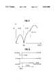
- FIG. 5is a diagram showing the relationship of gate current I g to floating gate voltage V fg* , and control gate voltage V cg when floating gate electrode FG is charged positively.
- hot carriers generated by the source-drain currentare injected into floating gate electrode FG.
- the types of hot carriersdepend upon the floating gate voltage, and are classfied, from the low voltage side as, hot holes (in the area of (H.H.) in FIG. 5) originating in a drain avalanche phenomenon, hot electrons (in the area of (H.E.) in FIG. 5) originating from a drain avalanche phenomenon, and channel hot electrons (in the area of (C.H.E.) in FIG. 5). It is important here that, when the floating gate voltage increases to the level indicated by V fg * in FIG.
- F-NFinler-Nordhein
- control gate electrode CGis set to 0 V, and a pulse of 5.0 V is applied for 0.5 seconds to source electrode S.
- the feedback mechanism between the floating gate electrode and the hot electron injection amount described aboveoperates so that the floating gate voltage converges to 2.0 V.
- the threshold level of control gate electrode CG after data erasurealso converges to a fixed value, which can suppress possible fluctuation of the threshold levels of the memory cells.
- the threshold level voltagecan be controlled within a range of about 0.7 V depending upon the dispersion of the configuration of source electrode S or some other factor.
- the source-drain current for causing the drain avalanche phenomenonis required, in addition to electrons to flow into floating gate electrode FG. Accordingly, there is a further problem in that the disposition to make the threshold voltages uniform after erasure of data results in higher power dissipation.
- the semi-conductor memorycomprises a plurality of n-type field effect transistors formed on a semi-conductor substrate, each transistor having a source electrode, a drain electrode, a floating gate electrode and a control gate electrode arrayed as non-volatile memory cells.
- the method of erasing datacomprises the steps of applying, for each of the n-type field effect transistors, a negative first voltage, to the control gate electrode, with respect to the potential at the source electrode and the drain electrode for the first application time so that the threshold level voltage of the field effect transistor which is lowest in speed of data erasing operation by the F-N tunnel current becomes the nearest value of the writing state within a predetermined range in the data erasing state, and applying, to each of the n-type field effect transistors, a positive second voltage, to the control gate electrode, with respect to the potential at the source electrode and the drain electrode for the second application time so that the threshold level voltage of the field effect transistor which is highest in speed of data writing operation by the F-N tunnel current becomes the nearest value of the writing state within the range of the data erasing state.
- a method of erasing data on a non-volatile semi-conductor memory of the typewherein a plurality of n-type field effect transistors formed on a semi-conductor substrate, each transistor having a source electrode, a drain electrode, a floating gate electrode and a control gate electrode arrayed as non-volatile memory cells.
- the method of erasing datacomprises the steps of applying, for each of the n-type field effect transistors, a positive first voltage, to the control gate electrodes, with respect to the potential at the source electrode and the drain electrode for a first application time so that the threshold level voltage of the field effect transistor which is lowest in speed of data erasing operation by the F-N tunnel current becomes the nearest value of writing state within a predetermined range of the data erasing state and applying, to each of the n-type field effect transistors, a negative second voltage, to the control gate electrode, with respect to the potential at the source electrode and the drain electrode for a second application time so that the threshold voltage of the field effect transistor which is highest in speed of data writing operation by the F-N tunnel current becomes the nearest value of writing state within the range of the data erasing state.
- the first application timeis preferably 0.01 second
- the first voltageis 19 volts
- the second applicaion timeis 0.1 second
- the second voltageis 14 volts.
- FIGS. 1(A) and 1(B)are a circuit diagram of a memory cell of a non-volatile semi-conductor memory as an object for erasure of data and a sectional view showing the structure of the memory, respectively;
- FIGS. 2(A) and 2(B)are a circuit diagram of the memory cell of a first embodiment of the present invention and a timing chart illustrating application of voltages to the electrodes of the memory cell upon erasure of data, respectively;
- FIG. 3is a characteristic diagram illustrating variations with respect to time of the memory cell threshold voltage upon erasure of data by the F-N tunnel current and upon injection of electrons into the floating gate;
- FIG. 4is a timing chart of application of voltages to the electrodes upon erasure of data of a memory cell of a second embodiment of the present invention
- FIG. 5is a characteristic diagram of the gate current with respect to the floating gate voltage and the control gate voltage of a memory cell according to a method of erasing data on a conventional non-volatile semi-conductor memory
- FIG. 6is a timing chart of application of voltages to the electrodes upon erasure of data of a memory cell of a conventional non-evaporate semiconductor memory.
- FIGS. 2(A) and 2(B)are a circuit diagram of a memory cell illustrating a first embodiment of the present invention and a timing chart of applying voltages to the electrodes of the memory cell upon erasure of data, respectively.
- the first embodimentis described in accordance with the progress of the disposition upon erasure of data. It is to be noted that the structure of the memory cell is the same as that of the conventional memory cell shown in FIGS. 1(A) and 1(B).
- drain electrode D, source electrode S and substrate Sub of each memory cellare set to 0 V while a pulse of -19 V and a pulse width of 0.01 second is applied to control gate electrode CG to remove electrons accumulated in floating gate electrode FG by an F-N tunnel current.
- the fluctuation with respect to application time of the threshold voltage of the memory cell upon erasure of data by the F-N tunnel currentis indicated by curves C1 and C2 in FIG. 3.
- All the memory cellsare designed as to have the same characteristics. However, actual memory cells typically have different characteristics. Therefore, data erasing operation speed fluctuates in every memory cells.
- a threshold voltageis lowered as the curve C1.
- the threshold voltagebecomes equal to 3 V which is the upper limit value (value nearest to that in the writing state) within the range of the threshold voltage set for the data erasing condition.
- the threshold voltage of another memory cell having highest erasing operation speedis lowered as the curve C2.
- the threshold voltagebecomes equal to 1 V.
- the threshold level voltagesfluctuate within the range of 2 V.
- the threshold voltage of the memory cell having lowest erasing operation speedis already equal to 3 V, and in this instance, even if a pulse of 14 V and 0.1 second is applied to control gate electrode CG, the threshold level voltage of the memory cell remains equal to 3 V, because injection of electrons into floating gate electrode FG by the F-N tunnel current does not take place unless the pulse width is longer than 0.1 second (refer to curve C3 in FIG. 3). Consequently, the threshold voltages converge approximately to 3 V, and dispersion of the threshold level voltages is suppressed.
- FIG. 4is a timing chart of application of voltages to the electrodes upon erasure of data of a memory cell of a second embodiment of the present invention. The second embodiment is described below in accordance with the procedure of the disposition upon erasure of data.
- drain electrode D, source electrode S and substrate Sub of each memory cellare set to 5 V while a pulse of -14 V and a pulse width of 0.01 second is applied to control gate electrode CG to remove electrons accumulated in floating gate electrode FG by the F-N tunnel current.
- drain electrode D, source electrode S and substrate Subare set to -5 V while a pulse of 9 V and a pulse width of 0.1 second is applied to control gate electrode CG to inject electrons into floating gate electrode FG by the F-N tunnel current.
- the absolute values of the voltages applied to the electrodesare different from those in the first embodiment, but the effective bias voltages between the control gate electrode and the source, drain and substrate electrodes, as well as the effects are exactly the same as those of the first embodiment.
- the absolute values of the voltages applied to the electrodesare lower than those in the first embodiment. Therefore, the second embodiment is more advantageous in terms of the voltage withstanding property and the required power supply.
- the present inventionsince it is constructed so that injection of electrons into floating gate electrode 3 using the F-N tunnel current is performed for a predetermined period of time after erasure of data, there is an advantage in that possible dispersion of the threshold level voltages after erasure of data can be suppressed. Further, since only the F-N tunnel current is used in order to control the threshold voltages to a fixed value, there is another advantage in that the voltage withstanding property of the junction between each diffused layer and the substrate is not degraded at all. Further, since the current which is produced when the threshold level voltages are controlled to a fixed value after erasure of data involves only electrons flowing into the floating gate electrode, there is a further advantage in that power dissipation can be reduced.
Landscapes
- Read Only Memory (AREA)
- Non-Volatile Memory (AREA)
Abstract
Description
Claims (7)
Applications Claiming Priority (2)
| Application Number | Priority Date | Filing Date | Title |
|---|---|---|---|
| JP30343192AJP2871355B2 (en) | 1992-11-13 | 1992-11-13 | Data erasing method for nonvolatile semiconductor memory device |
| JP4-303431 | 1992-11-13 |
Publications (1)
| Publication Number | Publication Date |
|---|---|
| US5412608Atrue US5412608A (en) | 1995-05-02 |
Family
ID=17920927
Family Applications (1)
| Application Number | Title | Priority Date | Filing Date |
|---|---|---|---|
| US08/150,809Expired - LifetimeUS5412608A (en) | 1992-11-13 | 1993-11-12 | Method of erasing data on non-volatile semi-conductor memory |
Country Status (5)
| Country | Link |
|---|---|
| US (1) | US5412608A (en) |
| EP (1) | EP0597722B1 (en) |
| JP (1) | JP2871355B2 (en) |
| KR (1) | KR960001321B1 (en) |
| DE (1) | DE69321685T2 (en) |
Cited By (13)
| Publication number | Priority date | Publication date | Assignee | Title |
|---|---|---|---|---|
| US5561387A (en)* | 1995-07-26 | 1996-10-01 | Taiwan Semiconductor Manufacturing Company Ltd | Method for measuring gate insulation layer thickness |
| US5838618A (en)* | 1997-09-11 | 1998-11-17 | Taiwan Semiconductor Manufacturing Company Ltd. | Bi-modal erase method for eliminating cycling-induced flash EEPROM cell write/erase threshold closure |
| US5959893A (en)* | 1996-06-29 | 1999-09-28 | Hyundai Electronics Industries Co., Ltd. | Method of erasing a flash memory device |
| US6005809A (en)* | 1998-06-19 | 1999-12-21 | Taiwan Semiconductor Manufacturing Company, Ltd. | Program and erase method for a split gate flash EEPROM |
| US6049486A (en)* | 1999-01-04 | 2000-04-11 | Taiwan Semiconductor Manufacturing Company | Triple mode erase scheme for improving flash EEPROM cell threshold voltage (VT) cycling closure effect |
| US6614693B1 (en) | 2002-03-19 | 2003-09-02 | Taiwan Semiconductor Manufacturing Company | Combination erase waveform to reduce oxide trapping centers generation rate of flash EEPROM |
| US6728140B2 (en) | 2001-12-05 | 2004-04-27 | Nexflash Technologies, Inc. | Threshold voltage convergence |
| US20060067125A1 (en)* | 2004-09-27 | 2006-03-30 | Macronix International Co., Ltd. | Programming and erasing method for charge-trapping memory devices |
| US20070036001A1 (en)* | 2005-07-29 | 2007-02-15 | Renesas Technology Corp. | Floating-gate nonvolatile semiconductor memory device |
| US20100124126A1 (en)* | 2008-11-14 | 2010-05-20 | Vishal Sarin | Erase voltage reduction in a non-volatile memory device |
| US20110286290A1 (en)* | 2010-05-20 | 2011-11-24 | Semiconductor Energy Laboratory Co., Ltd. | Driving method of semiconductor device |
| US8303642B1 (en)* | 2003-05-23 | 2012-11-06 | Advanced Cardiovascular Systems, Inc. | Metal injection molded tubing for drug eluting stents |
| CN114464222A (en)* | 2015-09-30 | 2022-05-10 | 禾瑞亚科技股份有限公司 | Methods to prevent loss of storage unit data |
Families Citing this family (5)
| Publication number | Priority date | Publication date | Assignee | Title |
|---|---|---|---|---|
| FR2718289B1 (en)* | 1994-03-30 | 1996-08-02 | Sgs Thomson Microelectronics | Electrically programmable memory cell. |
| US5903494A (en)* | 1994-03-30 | 1999-05-11 | Sgs-Thomson Microelectronics S.A. | Electrically programmable memory cell |
| WO1999031669A1 (en)* | 1997-12-18 | 1999-06-24 | Advanced Micro Devices, Inc. | Biasing method and structure for reducing band-to-band and/or avalanche currents during the erase of flash memory devices |
| JP4586219B2 (en)* | 1999-09-17 | 2010-11-24 | ソニー株式会社 | Erase method for nonvolatile semiconductor memory device |
| JP2008262626A (en)* | 2007-04-11 | 2008-10-30 | Renesas Technology Corp | Nonvolatile semiconductor memory |
Citations (3)
| Publication number | Priority date | Publication date | Assignee | Title |
|---|---|---|---|---|
| JPH02223097A (en)* | 1989-02-22 | 1990-09-05 | Toshiba Corp | Nonvolatile semiconductor memory |
| US5255237A (en)* | 1991-04-10 | 1993-10-19 | Nec Corporation | Method of erasing a nonvolatile semiconductor storage |
| US5295107A (en)* | 1992-03-02 | 1994-03-15 | Nec Corporation | Method of erasing data stored in flash type nonvolatile memory cell |
Family Cites Families (4)
| Publication number | Priority date | Publication date | Assignee | Title |
|---|---|---|---|---|
| US5132935A (en)* | 1990-04-16 | 1992-07-21 | Ashmore Jr Benjamin H | Erasure of eeprom memory arrays to prevent over-erased cells |
| JPH046698A (en)* | 1990-04-24 | 1992-01-10 | Mitsubishi Electric Corp | Non-volatile semiconductor memory device |
| JP2754887B2 (en)* | 1990-08-24 | 1998-05-20 | 三菱電機株式会社 | Nonvolatile semiconductor memory device and write / erase method therefor |
| JPH05235368A (en)* | 1992-02-19 | 1993-09-10 | Nec Corp | Erasing of data |
- 1992
- 1992-11-13JPJP30343192Apatent/JP2871355B2/ennot_activeExpired - Fee Related
- 1993
- 1993-11-12DEDE69321685Tpatent/DE69321685T2/ennot_activeExpired - Fee Related
- 1993-11-12EPEP93309051Apatent/EP0597722B1/ennot_activeExpired - Lifetime
- 1993-11-12USUS08/150,809patent/US5412608A/ennot_activeExpired - Lifetime
- 1993-11-13KRKR1019930024134Apatent/KR960001321B1/ennot_activeExpired - Fee Related
Patent Citations (3)
| Publication number | Priority date | Publication date | Assignee | Title |
|---|---|---|---|---|
| JPH02223097A (en)* | 1989-02-22 | 1990-09-05 | Toshiba Corp | Nonvolatile semiconductor memory |
| US5255237A (en)* | 1991-04-10 | 1993-10-19 | Nec Corporation | Method of erasing a nonvolatile semiconductor storage |
| US5295107A (en)* | 1992-03-02 | 1994-03-15 | Nec Corporation | Method of erasing data stored in flash type nonvolatile memory cell |
Non-Patent Citations (2)
| Title |
|---|
| Seiji Yamada et al, "A Self-Convergence Erasing Scheme For a Simple Stacked Gate Flash Eeprom", Sep. 1991 IEEE, pp. 11.4.1-11.4.4. |
| Seiji Yamada et al, A Self Convergence Erasing Scheme For a Simple Stacked Gate Flash Eeprom , Sep. 1991 IEEE , pp. 11.4.1 11.4.4.* |
Cited By (20)
| Publication number | Priority date | Publication date | Assignee | Title |
|---|---|---|---|---|
| US5561387A (en)* | 1995-07-26 | 1996-10-01 | Taiwan Semiconductor Manufacturing Company Ltd | Method for measuring gate insulation layer thickness |
| US5959893A (en)* | 1996-06-29 | 1999-09-28 | Hyundai Electronics Industries Co., Ltd. | Method of erasing a flash memory device |
| US5838618A (en)* | 1997-09-11 | 1998-11-17 | Taiwan Semiconductor Manufacturing Company Ltd. | Bi-modal erase method for eliminating cycling-induced flash EEPROM cell write/erase threshold closure |
| US6005809A (en)* | 1998-06-19 | 1999-12-21 | Taiwan Semiconductor Manufacturing Company, Ltd. | Program and erase method for a split gate flash EEPROM |
| US6049486A (en)* | 1999-01-04 | 2000-04-11 | Taiwan Semiconductor Manufacturing Company | Triple mode erase scheme for improving flash EEPROM cell threshold voltage (VT) cycling closure effect |
| US6728140B2 (en) | 2001-12-05 | 2004-04-27 | Nexflash Technologies, Inc. | Threshold voltage convergence |
| US6614693B1 (en) | 2002-03-19 | 2003-09-02 | Taiwan Semiconductor Manufacturing Company | Combination erase waveform to reduce oxide trapping centers generation rate of flash EEPROM |
| US8303642B1 (en)* | 2003-05-23 | 2012-11-06 | Advanced Cardiovascular Systems, Inc. | Metal injection molded tubing for drug eluting stents |
| US20090114976A1 (en)* | 2004-09-27 | 2009-05-07 | Hang-Ting Lue | Programming and Erasing Method for Charge-Trapping Memory Devices |
| US7274601B2 (en)* | 2004-09-27 | 2007-09-25 | Macronix International Co., Ltd. | Programming and erasing method for charge-trapping memory devices |
| US8023328B2 (en) | 2004-09-27 | 2011-09-20 | Macronix International Co., Ltd. | Memory device with charge trapping layer |
| US20060067125A1 (en)* | 2004-09-27 | 2006-03-30 | Macronix International Co., Ltd. | Programming and erasing method for charge-trapping memory devices |
| US20070036001A1 (en)* | 2005-07-29 | 2007-02-15 | Renesas Technology Corp. | Floating-gate nonvolatile semiconductor memory device |
| US20100124126A1 (en)* | 2008-11-14 | 2010-05-20 | Vishal Sarin | Erase voltage reduction in a non-volatile memory device |
| WO2010056504A3 (en)* | 2008-11-14 | 2010-07-29 | Micron Technology, Inc. | Erase voltage reduction in a non-volatile memory device |
| US8064267B2 (en) | 2008-11-14 | 2011-11-22 | Micron Technology, Inc. | Erase voltage reduction in a non-volatile memory device |
| US8391080B2 (en) | 2008-11-14 | 2013-03-05 | Micron Technology, Inc. | Erase voltage reduction in a non-volatile memory device |
| US20110286290A1 (en)* | 2010-05-20 | 2011-11-24 | Semiconductor Energy Laboratory Co., Ltd. | Driving method of semiconductor device |
| US8416622B2 (en)* | 2010-05-20 | 2013-04-09 | Semiconductor Energy Laboratory Co., Ltd. | Driving method of a semiconductor device with an inverted period having a negative potential applied to a gate of an oxide semiconductor transistor |
| CN114464222A (en)* | 2015-09-30 | 2022-05-10 | 禾瑞亚科技股份有限公司 | Methods to prevent loss of storage unit data |
Also Published As
| Publication number | Publication date |
|---|---|
| JP2871355B2 (en) | 1999-03-17 |
| EP0597722B1 (en) | 1998-10-21 |
| EP0597722A2 (en) | 1994-05-18 |
| JPH06150676A (en) | 1994-05-31 |
| EP0597722A3 (en) | 1995-05-24 |
| DE69321685D1 (en) | 1998-11-26 |
| KR960001321B1 (en) | 1996-01-25 |
| DE69321685T2 (en) | 1999-03-18 |
Similar Documents
| Publication | Publication Date | Title |
|---|---|---|
| US5412608A (en) | Method of erasing data on non-volatile semi-conductor memory | |
| JP3061924B2 (en) | Method of erasing nonvolatile storage device | |
| JP4422936B2 (en) | Erasing method of twin MONOS memory array | |
| KR101056797B1 (en) | Nonvolatile Semiconductor Memory | |
| EP0218342B1 (en) | Memory cells for integrated circuits | |
| US4630085A (en) | Erasable, programmable read-only memory device | |
| US7443731B2 (en) | Semiconductor nonvolatile memory device | |
| US4996571A (en) | Non-volatile semiconductor memory device erasing operation | |
| EP2416367A2 (en) | Multi-state memory cell with asymetric charge trapping | |
| US7515479B2 (en) | Nonvolatile semiconductor storage device and method for writing therein | |
| US5617358A (en) | Nonvolatile semiconductor memory device capable of converging threshold voltage with low power supply voltage | |
| JPH05235368A (en) | Erasing of data | |
| US4878199A (en) | Semiconductor memory device | |
| US5883835A (en) | Control method for non-volatile memory | |
| JPH04105368A (en) | Non-volatile semiconductor memory device and its writing/erasing method | |
| KR100663345B1 (en) | Nonvolatile Memory Cell Array with Common Drain Lines | |
| US5650964A (en) | Method of inhibiting degradation of ultra short channel charge-carrying devices during discharge | |
| KR100609216B1 (en) | Nonvolatile Memory Devices | |
| JPH06291327A (en) | Semiconductor non-volatile memory | |
| US5991203A (en) | Circuit and method of erasing a nonvolatile semiconductor memory | |
| JPH09260611A (en) | Electronic device | |
| KR100304000B1 (en) | A semiconductor memory and an erasing method for the semiconductor memory | |
| US6078522A (en) | Non-volatile semiconductor memory device | |
| JP3172347B2 (en) | Information writing method for nonvolatile semiconductor memory device | |
| KR20010033348A (en) | Biasing method and structure for reduceing band-to-band and/or avalanche currents during the erase of flash memory devices |
Legal Events
| Date | Code | Title | Description |
|---|---|---|---|
| AS | Assignment | Owner name:NEC CORPORATION, JAPAN Free format text:ASSIGNMENT OF ASSIGNORS INTEREST;ASSIGNOR:OYAMA, KEN-ICHI;REEL/FRAME:006868/0361 Effective date:19940107 | |
| STCF | Information on status: patent grant | Free format text:PATENTED CASE | |
| FEPP | Fee payment procedure | Free format text:PAYER NUMBER DE-ASSIGNED (ORIGINAL EVENT CODE: RMPN); ENTITY STATUS OF PATENT OWNER: LARGE ENTITY Free format text:PAYOR NUMBER ASSIGNED (ORIGINAL EVENT CODE: ASPN); ENTITY STATUS OF PATENT OWNER: LARGE ENTITY | |
| FEPP | Fee payment procedure | Free format text:PAYOR NUMBER ASSIGNED (ORIGINAL EVENT CODE: ASPN); ENTITY STATUS OF PATENT OWNER: LARGE ENTITY | |
| FPAY | Fee payment | Year of fee payment:4 | |
| FPAY | Fee payment | Year of fee payment:8 | |
| AS | Assignment | Owner name:NEC ELECTRONICS CORPORATION, JAPAN Free format text:ASSIGNMENT OF ASSIGNORS INTEREST;ASSIGNOR:NEC CORPORATION;REEL/FRAME:013758/0440 Effective date:20021101 | |
| FPAY | Fee payment | Year of fee payment:12 | |
| AS | Assignment | Owner name:RENESAS ELECTRONICS CORPORATION, JAPAN Free format text:CHANGE OF NAME;ASSIGNOR:NEC ELECTRONICS CORPORATION;REEL/FRAME:025149/0840 Effective date:20100401 |