US5412239A - Contact geometry for improved lateral MOSFET - Google Patents
Contact geometry for improved lateral MOSFETDownload PDFInfo
- Publication number
- US5412239A US5412239AUS08/062,507US6250793AUS5412239AUS 5412239 AUS5412239 AUS 5412239AUS 6250793 AUS6250793 AUS 6250793AUS 5412239 AUS5412239 AUS 5412239A
- Authority
- US
- United States
- Prior art keywords
- cells
- metal
- region
- source
- lateral mosfet
- Prior art date
- Legal status (The legal status is an assumption and is not a legal conclusion. Google has not performed a legal analysis and makes no representation as to the accuracy of the status listed.)
- Expired - Lifetime
Links
- 239000002184metalSubstances0.000claimsabstractdescription114
- 210000000746body regionAnatomy0.000claimsdescription15
- 239000000758substrateSubstances0.000claimsdescription13
- 239000000463materialSubstances0.000claimsdescription5
- 238000000926separation methodMethods0.000claimsdescription5
- 239000004065semiconductorSubstances0.000claimsdescription4
- 238000009792diffusion processMethods0.000description6
- 229910021420polycrystalline siliconInorganic materials0.000description6
- 229920005591polysiliconPolymers0.000description6
- 238000000034methodMethods0.000description3
- 230000000694effectsEffects0.000description2
- 230000001154acute effectEffects0.000description1
- 230000005684electric fieldEffects0.000description1
- 238000005530etchingMethods0.000description1
- 230000012447hatchingEffects0.000description1
- 238000004519manufacturing processMethods0.000description1
- 235000012054mealsNutrition0.000description1
- 229910052710siliconInorganic materials0.000description1
- 239000010703siliconSubstances0.000description1
Images


Classifications
- H—ELECTRICITY
- H10—SEMICONDUCTOR DEVICES; ELECTRIC SOLID-STATE DEVICES NOT OTHERWISE PROVIDED FOR
- H10D—INORGANIC ELECTRIC SEMICONDUCTOR DEVICES
- H10D30/00—Field-effect transistors [FET]
- H10D30/60—Insulated-gate field-effect transistors [IGFET]
- H10D30/64—Double-diffused metal-oxide semiconductor [DMOS] FETs
- H10D30/65—Lateral DMOS [LDMOS] FETs
- H—ELECTRICITY
- H10—SEMICONDUCTOR DEVICES; ELECTRIC SOLID-STATE DEVICES NOT OTHERWISE PROVIDED FOR
- H10D—INORGANIC ELECTRIC SEMICONDUCTOR DEVICES
- H10D64/00—Electrodes of devices having potential barriers
- H10D64/20—Electrodes characterised by their shapes, relative sizes or dispositions
- H10D64/23—Electrodes carrying the current to be rectified, amplified, oscillated or switched, e.g. sources, drains, anodes or cathodes
- H10D64/251—Source or drain electrodes for field-effect devices
- H10D64/257—Source or drain electrodes for field-effect devices for lateral devices wherein the source or drain electrodes are characterised by top-view geometrical layouts, e.g. interdigitated, semi-circular, annular or L-shaped electrodes
- H—ELECTRICITY
- H01—ELECTRIC ELEMENTS
- H01L—SEMICONDUCTOR DEVICES NOT COVERED BY CLASS H10
- H01L2924/00—Indexing scheme for arrangements or methods for connecting or disconnecting semiconductor or solid-state bodies as covered by H01L24/00
- H01L2924/0001—Technical content checked by a classifier
- H01L2924/0002—Not covered by any one of groups H01L24/00, H01L24/00 and H01L2224/00
- H—ELECTRICITY
- H10—SEMICONDUCTOR DEVICES; ELECTRIC SOLID-STATE DEVICES NOT OTHERWISE PROVIDED FOR
- H10D—INORGANIC ELECTRIC SEMICONDUCTOR DEVICES
- H10D62/00—Semiconductor bodies, or regions thereof, of devices having potential barriers
- H10D62/10—Shapes, relative sizes or dispositions of the regions of the semiconductor bodies; Shapes of the semiconductor bodies
- H10D62/113—Isolations within a component, i.e. internal isolations
- H10D62/115—Dielectric isolations, e.g. air gaps
- H10D62/116—Dielectric isolations, e.g. air gaps adjoining the input or output regions of field-effect devices, e.g. adjoining source or drain regions
- H—ELECTRICITY
- H10—SEMICONDUCTOR DEVICES; ELECTRIC SOLID-STATE DEVICES NOT OTHERWISE PROVIDED FOR
- H10D—INORGANIC ELECTRIC SEMICONDUCTOR DEVICES
- H10D62/00—Semiconductor bodies, or regions thereof, of devices having potential barriers
- H10D62/10—Shapes, relative sizes or dispositions of the regions of the semiconductor bodies; Shapes of the semiconductor bodies
- H10D62/124—Shapes, relative sizes or dispositions of the regions of semiconductor bodies or of junctions between the regions
- H10D62/126—Top-view geometrical layouts of the regions or the junctions
- H10D62/127—Top-view geometrical layouts of the regions or the junctions of cellular field-effect devices, e.g. multicellular DMOS transistors or IGBTs
- H—ELECTRICITY
- H10—SEMICONDUCTOR DEVICES; ELECTRIC SOLID-STATE DEVICES NOT OTHERWISE PROVIDED FOR
- H10D—INORGANIC ELECTRIC SEMICONDUCTOR DEVICES
- H10D62/00—Semiconductor bodies, or regions thereof, of devices having potential barriers
- H10D62/10—Shapes, relative sizes or dispositions of the regions of the semiconductor bodies; Shapes of the semiconductor bodies
- H10D62/17—Semiconductor regions connected to electrodes not carrying current to be rectified, amplified or switched, e.g. channel regions
- H10D62/393—Body regions of DMOS transistors or IGBTs
- H—ELECTRICITY
- H10—SEMICONDUCTOR DEVICES; ELECTRIC SOLID-STATE DEVICES NOT OTHERWISE PROVIDED FOR
- H10D—INORGANIC ELECTRIC SEMICONDUCTOR DEVICES
- H10D64/00—Electrodes of devices having potential barriers
- H10D64/20—Electrodes characterised by their shapes, relative sizes or dispositions
- H10D64/27—Electrodes not carrying the current to be rectified, amplified, oscillated or switched, e.g. gates
- H10D64/311—Gate electrodes for field-effect devices
- H10D64/411—Gate electrodes for field-effect devices for FETs
- H10D64/511—Gate electrodes for field-effect devices for FETs for IGFETs
- H10D64/514—Gate electrodes for field-effect devices for FETs for IGFETs characterised by the insulating layers
- H10D64/516—Gate electrodes for field-effect devices for FETs for IGFETs characterised by the insulating layers the thicknesses being non-uniform
- H—ELECTRICITY
- H10—SEMICONDUCTOR DEVICES; ELECTRIC SOLID-STATE DEVICES NOT OTHERWISE PROVIDED FOR
- H10D—INORGANIC ELECTRIC SEMICONDUCTOR DEVICES
- H10D64/00—Electrodes of devices having potential barriers
- H10D64/20—Electrodes characterised by their shapes, relative sizes or dispositions
- H10D64/27—Electrodes not carrying the current to be rectified, amplified, oscillated or switched, e.g. gates
- H10D64/311—Gate electrodes for field-effect devices
- H10D64/411—Gate electrodes for field-effect devices for FETs
- H10D64/511—Gate electrodes for field-effect devices for FETs for IGFETs
- H10D64/517—Gate electrodes for field-effect devices for FETs for IGFETs characterised by the conducting layers
- H10D64/519—Gate electrodes for field-effect devices for FETs for IGFETs characterised by the conducting layers characterised by their top-view geometrical layouts
Definitions
- This inventionrelates to lateral MOSFETs, and in particular, to an improved technique for establishing the contact between a metal layer and the source and drain cells of the MOSFET.
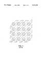
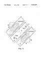
- the source and drain diffusionsare located on a single surface of a semiconductor substrate. While lateral MOSFETs can be constructed of long alternating stripes of source and drain regions separated by a gate stripe, it is well known that a closed cell arrangement typically provides a lower on-resistance in a given area. In such closed cell lateral MOSFET designs the cells are arranged in rows and columns as shown in FIG. 1, wherein cells alternate between source and drain regions in both columns and rows. Source and drain metal interconnection lines are then deposited diagonally, such that the source and drain metal lines alternate with one another across the face of the chip.
- FIGS. 2A and 2Billustrate top and cross-sectional views, respectively, of a typical cell.
- a diffusion 20 of N+ type materialis made in a P substrate 21.
- the N+ diffusionis accessed by a metal contact 22.
- the metal contact 22is surrounded laterally by a layer of gate material 23, typically polysilicon, which is separated from the top surface of substrate 21 by a gate oxide layer 24.
- a thermal oxide layer 25 and a thick oxide layer 26separate the polysilicon gate 23 from the metal contact 22.
- a minimal clearanceshown as "x" in FIGS. 2A and 2B, must maintained between them. If this minimal distance is not maintained, errors in alignment, for example, may create a short between the metal contact and the gate.
- a typical value of xis 1 ⁇ m.
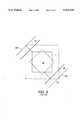
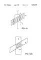
- FIG. 3is a top plan view of a junction between the metal contact 22 and one of the diagonal metal lines, designated by the reference numeral 30, which illustrates the problem that occurs at this location.
- Metal contact 22should be spaced at least a minimal distance from the edge of metal line 30, a distance which is designated as "v" in FIG. 3. Otherwise, a slight misalignment of the metal line may expose the contact. If the metal line does not cover the contact, then subsequent processing may etch holes through the silicon, destroying the junction and shorting out the device. It is well known that no portion of contact 22 should be left uncovered by metal line 30. As is evident from FIG. 3, metal 30 would have to be widened (see dashed lines 30A) to maintain the required separation between metal contact 22 and the edges of the meal line. This would very likely require that the source and drain cells be spaced further apart than is desirable fore minimizing the on-resistance of the MOSFET.
- the minimal distance vcould be maintained by rotating metal contact 22 through a 45° angle (as shown by the dashed lines). However, this will result in metal contact 22 being closer than the minimal distance x to the polysilicon gate 23. (The opening in gate 23 is illustrated by the dotted and dashed line in FIG. 3.)
- the cross-sectional area of the metal contactis maximized, while the minimal clearance between both the edge of the gate and the edge of a diagonal metal line is maintained.
- a metal contact to a region of a lateral MOSFETis structured such that its corners which face the edges of an overlying diagonal metal line are truncated. This maximizes the cross-sectional area of the contact while maintaining minimal clearance between the edges of the gate and the metal line.
- the cross-sectional shape of metal contactis normally rectangular. By truncating the two opposite corners, a six-sided figure is formed, although the sides of the figure are not necessarily equal. In an extreme case, if the truncation goes all the way back to an adjacent corner of the rectangle, a parallelogram is formed.
- This techniquecan be used in various types of MOSFETs, including those which have a body contact region separated from the source and drain cells, those which have a body contact region within each source cell, and those in which the drain cells are smaller than the source cells.
- This techniquecan also be used in configuring vias which extend between diagonal metal lines and an overlying metal layer.
- FIG. 1illustrates the layout of source and drain cells in a typical lateral MOSFET.
- FIGS. 2A and 2Billustrate top plan and cross-sectional views, respectively, of a cell in a typical lateral MOSFET.
- FIG. 3illustrates a top plan view of a junction between a metal contact and a diagonal metal line.
- FIG. 4illustrates the six-sided cross-sectional shape of a metal contact in accordance with the invention.
- FIG. 5illustrates an alternative metal contact in accordance with the invention, whose cross-sectional shape is a parallelogram.
- FIGS. 6A and 6Billustrate a top plan view and a perspective view, respectively, of a conventional lateral MOSFET without a local source/body short.
- FIGS. 7A and 7Billustrate a top plan view and a perspective view, respectively, of a conventional lateral MOSFET with a local source/body short.
- FIGS. 8A and 8Billustrate a top plan view and a perspective view, respectively, of a drain-enclosed lateral DMOS with a local source/body short.
- FIG. 9illustrates a perspective view of a drain-enclosed lateral DMOS wherein the gate layer does not extend the entire distance between the drain and the source/body cells.
- FIG. 10illustrates a drain-enclosed lateral DMOS in which the gate layer extends partially over a field oxide layer.
- FIG. 11illustrates a plan view of a lateral MOSFET in which the source/body cells are larger than the drain cells.
- FIG. 12illustrates a cross-sectional view of a lateral MOSFET cell including two overlying metal layers.
- FIG. 13illustrates a general plan view of the two metal layers.
- FIGS. 14A and 14Billustrate detailed plan views of a via between lines in the two metal layers.
- FIG. 15illustrates a pattern of vias used to interconnect diagonal metal lines to overlying vertical metal lines in accordance with another aspect of the invention.
- FIG. 4illustrates a top view of a metal contact in accordance with this invention.
- Metal contact 22Ais similar to contact 22 (FIG. 3) except that the corners of the contact facing the edges of diagonal metal line 30 have been truncated.
- the minimal distance x between the metal contact and the polysilicon gate 23 and the minimal distance v between the metal contact and the edge of metal line 30have been maintained, while the cross-sectional area of metal contacts 22A has been maximized. Maximizing the cross-sectional area of metal contact 22A helps to minimize the on-resistance of the MOSFET. Truncating the corners of metal contact 22A eliminates the need to widen metal line 30.
- a wide metal lineis desirable to minimize the metal line's contribution to the MOSFET's resistance and to maximize its current handling capability, a wide metal line is only desirable when it does not require larger spacings between devices.
- R dsis the on-resistance of the MOSFET
- Lis the distance separating the sources and the drains (i.e., the channel length)
- Wis the total length of all drain edges which face sources. Avoiding the need to widen the metal line 30 allows one to maintain the cell separation L at a desired value, whereas if metal line 30 were widened the effect would be to increase L. Thus the overall effect of truncating the corners of metal contact 22A is to maintain R ds at an minimum value.
- FIG. 5illustrates a gate layer 50 which has a rectangular opening and a metal line 51 which is oriented at an oblique angle other than 45° to the sides of the gate opening.
- truncating the corners of metal contact 52may yield the shape of a parallelogram.
- FIGS. 6-10illustrate several of these possibilities.
- FIG. 6Aillustrates a top plan view
- FIG. 6Billustrates a perspective view of a conventional lateral MOSFET with a remote body contact region.
- the source and drain cellsinclude N+ diffusions in a P substrate, and a P+ body contact diffusion is formed at the edge of the MOSFET. Whether or not the body is shorted to the source electrically depends on the circuit application. In any event, providing a P+ diffusion only at the periphery reduces cell size and thereby improves on-resistance (i.e., more cells/area).
- FIG. 7Aillustrates a top plan view and FIG. 7B a perspective view of a MOSFET which has a local P+ body contact region in each source cell.
- the source and body regionsmust be shorted, and this requires a larger metal contact than the source cells in the embodiment of FIGS. 6A and 6B.
- FIG. 8Aillustrates a top plan view and FIG. 8B a perspective view of a drain-enclosed, lateral double diffused MOSFET (DMOS).
- the substrateis N-type material
- the channelis formed in the P body region, which extends under the gate.
- the total distance between the cellsis the summation of the width of the channel region (L) and the width (L D ) of a "drift" region which extends between the drain and the P body region.
- the metal contactmust create a short between the source and body regions in each source/body cell.
- FIGS. 8A and 8Billustrate a perspective view of a lateral DMOS in which the gate does not cover the entire area between the source/body region and the drain region, i.e., the "drift" region is left largely uncovered by the gate. This reduces the electric field in the drift region, with the result that this embodiment allows a higher voltage than the embodiment shown in FIGS. 8A and 8B.
- FIG. 10illustrates a perspective view of an embodiment similar to that shown in FIG. 9, except that the gate extends over a relatively thick field oxide. This further increases the capability of the MOSFET to withstand high voltages.
- the metal contacts to the source and drain cellsare essentially the same size. In the embodiments shown in FIGS. 7-10, however, the metal contacts extending to the source/body regions are normally somewhat larger than those which contact the drain regions.
- This type of arrangementis illustrated generally in the top view of FIG. 11, where a gate layer 80 has large openings 80S for the source/body cells and small openings 80D for the drain cells.
- Metal lines 81, 82 and 83intersect the cells diagonally. The cross hatching indicates the metal contacts.
- the metal contacts in the source/body cellsmust be truncated to maintain a minimal distance from the edges of the metal lines whereas the metal contacts in the drain cells need not be truncated.
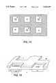
- FIG. 12shows a first metal layer 90 separated from a second layer 91 by a dielectric layer 92.
- a via 93extends through dielectric layer 92 to make contact between metal layers between 90 and 91.
- via 93is shown directly over the metal contact for purposes of illustration, in general it is common for the via to be spaced apart from the contact.
- FIG. 13illustrates how contact might be made between diagonal lines of metal layer 90 and vertical lines of metal layer 91 to provide connections to drain and source terminals at the edges of the MOSFET. (The location of the vias are indicated by dots.)
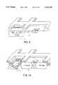
- FIG. 14Aillustrates a detailed top view of a single intersection between a diagonal line of metal layer 90 and a vertical line of metal layer 91.
- a via 92connects the two metal lines.
- a margin "u"should be maintained between the edges of lines 90 and 91 and the perimeter of via 92.
- FIG. 14Aindicates, this yields a via whose cross-section is in the shape of a parallelogram.
- FIG. 14Billustrates a via 93 having a six-sided shape similar to the one shown previously for use with a contact. The advantage of a six-sided shape over the parallelogram of FIG. 14A is that it avoids acute angles, which may complicate the manufacture of transistors.
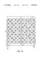
- FIG. 15Illustrated in FIG. 15 is a plan view of a number of diagonal metal lines 100 in a first metal layer overlain by two vertical metal interconnect lines 101 and 102 in a second metal layer.
- Source and drain cells 103designated “S” and “D", respectively
- vias 104cross-hatched extending between the first and second metal layers are also shown. It will be noted that along any given metal line 100, the cells 103 and vias 104 alternate, while the source cells are connected to interconnect line 101 and the drain cells are connected to interconnect line 102. This alternating via/contact layout minimizes the distance which current must flow exclusively in the first metal layer before reaching a via, thereby reducing metal resistance and current density in the metal lines 100.
Landscapes
- Insulated Gate Type Field-Effect Transistor (AREA)
- Electrodes Of Semiconductors (AREA)
- Internal Circuitry In Semiconductor Integrated Circuit Devices (AREA)
Abstract
Description
Claims (15)
Priority Applications (5)
| Application Number | Priority Date | Filing Date | Title |
|---|---|---|---|
| US08/062,507US5412239A (en) | 1993-05-14 | 1993-05-14 | Contact geometry for improved lateral MOSFET |
| DE69417798TDE69417798T2 (en) | 1993-05-14 | 1994-05-12 | Lateral MOSFET with contact structure |
| EP94303417AEP0624909B1 (en) | 1993-05-14 | 1994-05-12 | Lateral MOSFET with contact structure |
| JP12419994AJP3943604B2 (en) | 1993-05-14 | 1994-05-13 | Lateral MOSFET |
| JP2006319878AJP4597945B2 (en) | 1993-05-14 | 2006-11-28 | Lateral MOSFET |
Applications Claiming Priority (1)
| Application Number | Priority Date | Filing Date | Title |
|---|---|---|---|
| US08/062,507US5412239A (en) | 1993-05-14 | 1993-05-14 | Contact geometry for improved lateral MOSFET |
Publications (1)
| Publication Number | Publication Date |
|---|---|
| US5412239Atrue US5412239A (en) | 1995-05-02 |
Family
ID=22042930
Family Applications (1)
| Application Number | Title | Priority Date | Filing Date |
|---|---|---|---|
| US08/062,507Expired - LifetimeUS5412239A (en) | 1993-05-14 | 1993-05-14 | Contact geometry for improved lateral MOSFET |
Country Status (4)
| Country | Link |
|---|---|
| US (1) | US5412239A (en) |
| EP (1) | EP0624909B1 (en) |
| JP (2) | JP3943604B2 (en) |
| DE (1) | DE69417798T2 (en) |
Cited By (26)
| Publication number | Priority date | Publication date | Assignee | Title |
|---|---|---|---|---|
| WO1996010267A1 (en)* | 1994-09-27 | 1996-04-04 | Micrel, Inc. | High voltage lateral dmos device with enhanced drift region |
| US5648288A (en)* | 1992-03-20 | 1997-07-15 | Siliconix Incorporated | Threshold adjustment in field effect semiconductor devices |
| US5672894A (en)* | 1994-10-20 | 1997-09-30 | Nippondenso Co., Ltd. | Semiconductor device |
| US5945709A (en)* | 1994-12-30 | 1999-08-31 | Siliconix Incorporated | Integrated circuit die having thick bus to reduce distributed resistance |
| US6133598A (en)* | 1997-05-29 | 2000-10-17 | Lg Semicon Co., Ltd. | Semiconductor device with diagonal capacitor bit line and fabrication method thereof |
| US6274896B1 (en) | 2000-01-14 | 2001-08-14 | Lexmark International, Inc. | Drive transistor with fold gate |
| US6479877B2 (en) | 2000-04-19 | 2002-11-12 | Denso Corporation | Semiconductor device for load drive circuit |
| US20040075113A1 (en)* | 2002-10-15 | 2004-04-22 | Yoshiaki Nakayama | Semiconductor equipment |
| US20040084776A1 (en)* | 2002-10-30 | 2004-05-06 | Yutaka Fukuda | Semiconductor equipment |
| US20040119154A1 (en)* | 2002-12-20 | 2004-06-24 | Michael Briere | Flip chip fet device |
| US20040125577A1 (en)* | 2002-12-27 | 2004-07-01 | Patrizio Vinciarelli | Low loss, high density array interconnection |
| US20050253183A1 (en)* | 2004-04-22 | 2005-11-17 | Kabushiki Kaisha Toshiba | Non-volatile semiconductor memory device and method of fabricating the same |
| US7109558B2 (en) | 2001-06-06 | 2006-09-19 | Denso Corporation | Power MOS transistor having capability for setting substrate potential independently of source potential |
| US7185302B1 (en)* | 2004-06-01 | 2007-02-27 | Polar Semiconductor, Inc. | Method for generating layouts by chamfering corners of polygons |
| US20090302479A1 (en)* | 2008-06-06 | 2009-12-10 | Avago Technologies Wireless Ip (Singapore) Pte. Ltd. | Semiconductor structures having vias |
| CN101246906B (en)* | 2007-02-16 | 2012-01-04 | 电力集成公司 | Gate Pullback at the End of High Voltage Transistor Structures |
| US8169081B1 (en) | 2007-12-27 | 2012-05-01 | Volterra Semiconductor Corporation | Conductive routings in integrated circuits using under bump metallization |
| US20130221437A1 (en)* | 2012-02-29 | 2013-08-29 | Standard Microsystems Corporation | Transistor with minimized resistance |
| US20130320522A1 (en)* | 2012-05-30 | 2013-12-05 | Taiwan Semiconductor Manufacturing Company, Ltd. | Re-distribution Layer Via Structure and Method of Making Same |
| US20140206301A1 (en)* | 2012-03-27 | 2014-07-24 | Hemasundar Mohan Geddada | Transceiver with an integrated rx/tx configurable passive network |
| US9024327B2 (en) | 2007-12-14 | 2015-05-05 | Cree, Inc. | Metallization structure for high power microelectronic devices |
| US9543396B2 (en) | 2013-12-13 | 2017-01-10 | Power Integrations, Inc. | Vertical transistor device structure with cylindrically-shaped regions |
| US20170278757A1 (en)* | 2007-12-03 | 2017-09-28 | Infineon Technologies Ag | Methods of Manufacturing Semiconductor Devices |
| CN109390396A (en)* | 2013-08-21 | 2019-02-26 | 晶元光电股份有限公司 | High electron mobility transistor |
| US10325988B2 (en) | 2013-12-13 | 2019-06-18 | Power Integrations, Inc. | Vertical transistor device structure with cylindrically-shaped field plates |
| US20220067259A1 (en)* | 2020-08-31 | 2022-03-03 | Taiwan Semiconductor Manufacturing Company Ltd. | Structure and method of non-rectangular cell in semiconductor device |
Families Citing this family (21)
| Publication number | Priority date | Publication date | Assignee | Title |
|---|---|---|---|---|
| JP3570052B2 (en)* | 1995-01-19 | 2004-09-29 | セイコーエプソン株式会社 | Semiconductor memory device and method of manufacturing the same |
| JP2997179B2 (en)* | 1995-01-27 | 2000-01-11 | モトローラ株式会社 | Power MOS transistor |
| EP0766309A3 (en)* | 1995-08-28 | 1998-04-29 | Texas Instruments Incorporated | Field effect transistor which multi-level metallisation related to integrated circuits |
| US7941675B2 (en) | 2002-12-31 | 2011-05-10 | Burr James B | Adaptive power control |
| US7323367B1 (en) | 2002-12-31 | 2008-01-29 | Transmeta Corporation | Diagonal deep well region for routing body-bias voltage for MOSFETS in surface well regions |
| US6936898B2 (en) | 2002-12-31 | 2005-08-30 | Transmeta Corporation | Diagonal deep well region for routing body-bias voltage for MOSFETS in surface well regions |
| US7228242B2 (en) | 2002-12-31 | 2007-06-05 | Transmeta Corporation | Adaptive power control based on pre package characterization of integrated circuits |
| US7174528B1 (en) | 2003-10-10 | 2007-02-06 | Transmeta Corporation | Method and apparatus for optimizing body bias connections in CMOS circuits using a deep n-well grid structure |
| US7649402B1 (en) | 2003-12-23 | 2010-01-19 | Tien-Min Chen | Feedback-controlled body-bias voltage source |
| US7129771B1 (en) | 2003-12-23 | 2006-10-31 | Transmeta Corporation | Servo loop for well bias voltage source |
| US7012461B1 (en) | 2003-12-23 | 2006-03-14 | Transmeta Corporation | Stabilization component for a substrate potential regulation circuit |
| US7692477B1 (en) | 2003-12-23 | 2010-04-06 | Tien-Min Chen | Precise control component for a substrate potential regulation circuit |
| US7645673B1 (en) | 2004-02-03 | 2010-01-12 | Michael Pelham | Method for generating a deep N-well pattern for an integrated circuit design |
| US7388260B1 (en) | 2004-03-31 | 2008-06-17 | Transmeta Corporation | Structure for spanning gap in body-bias voltage routing structure |
| US7774625B1 (en) | 2004-06-22 | 2010-08-10 | Eric Chien-Li Sheng | Adaptive voltage control by accessing information stored within and specific to a microprocessor |
| US7562233B1 (en) | 2004-06-22 | 2009-07-14 | Transmeta Corporation | Adaptive control of operating and body bias voltages |
| US7598573B2 (en) | 2004-11-16 | 2009-10-06 | Robert Paul Masleid | Systems and methods for voltage distribution via multiple epitaxial layers |
| JP4372046B2 (en) | 2005-05-18 | 2009-11-25 | 株式会社東芝 | Semiconductor device |
| US7305647B1 (en) | 2005-07-28 | 2007-12-04 | Transmeta Corporation | Using standard pattern tiles and custom pattern tiles to generate a semiconductor design layout having a deep well structure for routing body-bias voltage |
| JP5066928B2 (en)* | 2007-02-08 | 2012-11-07 | 株式会社デンソー | Semiconductor device |
| JP2015170607A (en)* | 2014-03-04 | 2015-09-28 | 株式会社デンソー岩手 | lateral MOSFET |
Citations (3)
| Publication number | Priority date | Publication date | Assignee | Title |
|---|---|---|---|---|
| US4012764A (en)* | 1974-12-04 | 1977-03-15 | Hitachi, Ltd. | Semiconductor integrated circuit device |
| US4196443A (en)* | 1978-08-25 | 1980-04-01 | Rca Corporation | Buried contact configuration for CMOS/SOS integrated circuits |
| US4951101A (en)* | 1988-08-25 | 1990-08-21 | Micrel Incorporated | Diamond shorting contact for semiconductors |
Family Cites Families (11)
| Publication number | Priority date | Publication date | Assignee | Title |
|---|---|---|---|---|
| US4148047A (en)* | 1978-01-16 | 1979-04-03 | Honeywell Inc. | Semiconductor apparatus |
| JPS6053085A (en)* | 1983-09-02 | 1985-03-26 | Hitachi Ltd | Junction field effect transistor |
| US4636825A (en)* | 1985-10-04 | 1987-01-13 | Fairchild Semiconductor Corporation | Distributed field effect transistor structure |
| IT1213027B (en)* | 1986-01-24 | 1989-12-07 | Sgs Microelettrica Spa | DENSITY.! SEMICONDUCTOR INTEGRATED CIRCUIT, IN PARTICULAR OF THE TYPE INCLUDING HIGH VOLTAGE DEVICES AND HIGH SIGNAL PROCESSING DEVICES |
| JPH07112064B2 (en)* | 1986-02-10 | 1995-11-29 | 株式会社東芝 | Insulated gate field effect transistor |
| JPH02268467A (en)* | 1989-04-10 | 1990-11-02 | New Japan Radio Co Ltd | Semiconductor integrated circuit |
| JPH03239369A (en)* | 1990-02-16 | 1991-10-24 | Nissan Motor Co Ltd | semiconductor equipment |
| JPH04109677A (en)* | 1990-08-29 | 1992-04-10 | Seiko Instr Inc | MOS transistor |
| EP0487022B1 (en)* | 1990-11-23 | 1997-04-23 | Texas Instruments Incorporated | A method of simultaneously fabricating an insulated gate-field-effect transistor and a bipolar transistor |
| EP0566262A2 (en)* | 1992-04-15 | 1993-10-20 | National Semiconductor Corporation | Field effect transistor with a deep P body contacted by the source electrode |
| JP3248251B2 (en)* | 1992-07-31 | 2002-01-21 | 松下電器産業株式会社 | Method for producing electrode foil for aluminum electrolytic capacitor |
- 1993
- 1993-05-14USUS08/062,507patent/US5412239A/ennot_activeExpired - Lifetime
- 1994
- 1994-05-12DEDE69417798Tpatent/DE69417798T2/ennot_activeExpired - Fee Related
- 1994-05-12EPEP94303417Apatent/EP0624909B1/ennot_activeExpired - Lifetime
- 1994-05-13JPJP12419994Apatent/JP3943604B2/ennot_activeExpired - Lifetime
- 2006
- 2006-11-28JPJP2006319878Apatent/JP4597945B2/ennot_activeExpired - Lifetime
Patent Citations (3)
| Publication number | Priority date | Publication date | Assignee | Title |
|---|---|---|---|---|
| US4012764A (en)* | 1974-12-04 | 1977-03-15 | Hitachi, Ltd. | Semiconductor integrated circuit device |
| US4196443A (en)* | 1978-08-25 | 1980-04-01 | Rca Corporation | Buried contact configuration for CMOS/SOS integrated circuits |
| US4951101A (en)* | 1988-08-25 | 1990-08-21 | Micrel Incorporated | Diamond shorting contact for semiconductors |
Cited By (45)
| Publication number | Priority date | Publication date | Assignee | Title |
|---|---|---|---|---|
| US5648288A (en)* | 1992-03-20 | 1997-07-15 | Siliconix Incorporated | Threshold adjustment in field effect semiconductor devices |
| US5517046A (en)* | 1993-11-19 | 1996-05-14 | Micrel, Incorporated | High voltage lateral DMOS device with enhanced drift region |
| WO1996010267A1 (en)* | 1994-09-27 | 1996-04-04 | Micrel, Inc. | High voltage lateral dmos device with enhanced drift region |
| US5672894A (en)* | 1994-10-20 | 1997-09-30 | Nippondenso Co., Ltd. | Semiconductor device |
| US6159841A (en)* | 1994-12-30 | 2000-12-12 | Siliconix Incorporated | Method of fabricating lateral power MOSFET having metal strap layer to reduce distributed resistance |
| US5945709A (en)* | 1994-12-30 | 1999-08-31 | Siliconix Incorporated | Integrated circuit die having thick bus to reduce distributed resistance |
| US6344391B1 (en) | 1997-05-29 | 2002-02-05 | Hyundai Electronics Industries Co., Ltd. | Fabrication method of semiconductor device with diagonal capacitor bit line |
| US6133598A (en)* | 1997-05-29 | 2000-10-17 | Lg Semicon Co., Ltd. | Semiconductor device with diagonal capacitor bit line and fabrication method thereof |
| US6274896B1 (en) | 2000-01-14 | 2001-08-14 | Lexmark International, Inc. | Drive transistor with fold gate |
| US6479877B2 (en) | 2000-04-19 | 2002-11-12 | Denso Corporation | Semiconductor device for load drive circuit |
| US7109558B2 (en) | 2001-06-06 | 2006-09-19 | Denso Corporation | Power MOS transistor having capability for setting substrate potential independently of source potential |
| US6958543B2 (en) | 2002-10-15 | 2005-10-25 | Denso Corporation | Semiconductor equipment with lateral and vertical MOS regions |
| US20040075113A1 (en)* | 2002-10-15 | 2004-04-22 | Yoshiaki Nakayama | Semiconductor equipment |
| US20040084776A1 (en)* | 2002-10-30 | 2004-05-06 | Yutaka Fukuda | Semiconductor equipment |
| FR2846793A1 (en)* | 2002-10-30 | 2004-05-07 | Denso Corp | SEMICONDUCTOR EQUIPMENT INCLUDING UPPER AND LOWER LAYER WIRING |
| US6903460B2 (en) | 2002-10-30 | 2005-06-07 | Denso Corporation | Semiconductor equipment |
| US7166898B2 (en)* | 2002-12-20 | 2007-01-23 | Picor Corporation | Flip chip FET device |
| US6969909B2 (en) | 2002-12-20 | 2005-11-29 | Vlt, Inc. | Flip chip FET device |
| US20050269647A1 (en)* | 2002-12-20 | 2005-12-08 | Vlt Corporation, A Texas Corporation | Flip chip FET device |
| US20040119154A1 (en)* | 2002-12-20 | 2004-06-24 | Michael Briere | Flip chip fet device |
| US7038917B2 (en)* | 2002-12-27 | 2006-05-02 | Vlt, Inc. | Low loss, high density array interconnection |
| US20040125577A1 (en)* | 2002-12-27 | 2004-07-01 | Patrizio Vinciarelli | Low loss, high density array interconnection |
| US20050253183A1 (en)* | 2004-04-22 | 2005-11-17 | Kabushiki Kaisha Toshiba | Non-volatile semiconductor memory device and method of fabricating the same |
| US7185302B1 (en)* | 2004-06-01 | 2007-02-27 | Polar Semiconductor, Inc. | Method for generating layouts by chamfering corners of polygons |
| CN101246906B (en)* | 2007-02-16 | 2012-01-04 | 电力集成公司 | Gate Pullback at the End of High Voltage Transistor Structures |
| CN102412267B (en)* | 2007-02-16 | 2015-01-07 | 电力集成公司 | Grid pulling at end of high voltage transistor structure |
| CN102412267A (en)* | 2007-02-16 | 2012-04-11 | 电力集成公司 | High-voltage Vertical Fet |
| US9601613B2 (en) | 2007-02-16 | 2017-03-21 | Power Integrations, Inc. | Gate pullback at ends of high-voltage vertical transistor structure |
| US20170278757A1 (en)* | 2007-12-03 | 2017-09-28 | Infineon Technologies Ag | Methods of Manufacturing Semiconductor Devices |
| US9024327B2 (en) | 2007-12-14 | 2015-05-05 | Cree, Inc. | Metallization structure for high power microelectronic devices |
| US8169081B1 (en) | 2007-12-27 | 2012-05-01 | Volterra Semiconductor Corporation | Conductive routings in integrated circuits using under bump metallization |
| US8664767B2 (en) | 2007-12-27 | 2014-03-04 | Volterra Semiconductor Corporation | Conductive routings in integrated circuits using under bump metallization |
| US8933520B1 (en) | 2007-12-27 | 2015-01-13 | Volterra Semiconductor LLC | Conductive routings in integrated circuits using under bump metallization |
| US20090302479A1 (en)* | 2008-06-06 | 2009-12-10 | Avago Technologies Wireless Ip (Singapore) Pte. Ltd. | Semiconductor structures having vias |
| US8836029B2 (en)* | 2012-02-29 | 2014-09-16 | Smsc Holdings S.A.R.L. | Transistor with minimized resistance |
| US20130221437A1 (en)* | 2012-02-29 | 2013-08-29 | Standard Microsystems Corporation | Transistor with minimized resistance |
| US20140206301A1 (en)* | 2012-03-27 | 2014-07-24 | Hemasundar Mohan Geddada | Transceiver with an integrated rx/tx configurable passive network |
| US20130320522A1 (en)* | 2012-05-30 | 2013-12-05 | Taiwan Semiconductor Manufacturing Company, Ltd. | Re-distribution Layer Via Structure and Method of Making Same |
| CN109390396A (en)* | 2013-08-21 | 2019-02-26 | 晶元光电股份有限公司 | High electron mobility transistor |
| US9543396B2 (en) | 2013-12-13 | 2017-01-10 | Power Integrations, Inc. | Vertical transistor device structure with cylindrically-shaped regions |
| US10325988B2 (en) | 2013-12-13 | 2019-06-18 | Power Integrations, Inc. | Vertical transistor device structure with cylindrically-shaped field plates |
| US20220067259A1 (en)* | 2020-08-31 | 2022-03-03 | Taiwan Semiconductor Manufacturing Company Ltd. | Structure and method of non-rectangular cell in semiconductor device |
| US12039242B2 (en)* | 2020-08-31 | 2024-07-16 | Taiwan Semiconductor Manufacturing Company Ltd. | Structure and method of non-rectangular cell in semiconductor device |
| US20240330561A1 (en)* | 2020-08-31 | 2024-10-03 | Taiwan Semiconductor Manufacturing Company Ltd. | Structure and method of rectangular cell in semiconductor device |
| US12353816B2 (en)* | 2020-08-31 | 2025-07-08 | Taiwan Semiconductor Manufacturing Company Ltd. | Structure and method of rectangular cell in semiconductor device |
Also Published As
| Publication number | Publication date |
|---|---|
| EP0624909B1 (en) | 1999-04-14 |
| DE69417798D1 (en) | 1999-05-20 |
| JP3943604B2 (en) | 2007-07-11 |
| JPH07142729A (en) | 1995-06-02 |
| DE69417798T2 (en) | 1999-08-26 |
| EP0624909A2 (en) | 1994-11-17 |
| JP4597945B2 (en) | 2010-12-15 |
| EP0624909A3 (en) | 1995-09-20 |
| JP2007096341A (en) | 2007-04-12 |
Similar Documents
| Publication | Publication Date | Title |
|---|---|---|
| US5412239A (en) | Contact geometry for improved lateral MOSFET | |
| JP3136885B2 (en) | Power MOSFET | |
| US5672528A (en) | Method for making semiconductor device having field limiting ring | |
| US6767779B2 (en) | Asymmetrical MOSFET layout for high currents and high speed operation | |
| EP0234276A2 (en) | Insulated gate type field effect transistor | |
| EP0282705B1 (en) | Fet structure arrangement having low on resistance | |
| US5763914A (en) | Cell topology for power transistors with increased packing density | |
| EP0237361B1 (en) | Semiconductor memory device | |
| US6885071B2 (en) | Semiconductor integrated circuit making use of standard cells | |
| US6492691B2 (en) | High integration density MOS technology power device structure | |
| US6730963B2 (en) | Minimum sized cellular MOS-gated device geometry | |
| JPS63311766A (en) | Mis power transistor | |
| US6060761A (en) | Lateral type transistor | |
| US4961101A (en) | Semiconductor MOSFET device with offset regions | |
| JPH08250600A (en) | Semiconductor device and manufacturing method thereof | |
| US6713822B2 (en) | Semiconductor device | |
| US6541827B1 (en) | Semiconductor device having a patterned insulated gate | |
| KR100225944B1 (en) | Semiconductor device having variable drain current type transistor | |
| JPH1168092A (en) | Groove type semiconductor device | |
| JPH09129878A (en) | Semiconductor device | |
| US4302765A (en) | Geometry for fabricating enhancement and depletion-type, pull-up field effect transistor devices | |
| EP0100677B1 (en) | Semiconductor devices including lateral-type transistors | |
| KR0184262B1 (en) | Semiconductor device | |
| US7022564B1 (en) | Method of forming a low thermal resistance device and structure | |
| JPH10326876A (en) | Semiconductor device |
Legal Events
| Date | Code | Title | Description |
|---|---|---|---|
| STPP | Information on status: patent application and granting procedure in general | Free format text:APPLICATION UNDERGOING PREEXAM PROCESSING | |
| AS | Assignment | Owner name:SILICONIX INCORPORATED Free format text:ASSIGNMENT OF ASSIGNORS INTEREST;ASSIGNOR:WILLIAMS, RICHARD K.;REEL/FRAME:006773/0345 Effective date:19930826 | |
| CC | Certificate of correction | ||
| FPAY | Fee payment | Year of fee payment:4 | |
| FPAY | Fee payment | Year of fee payment:8 | |
| REMI | Maintenance fee reminder mailed | ||
| FPAY | Fee payment | Year of fee payment:12 | |
| AS | Assignment | Owner name:COMERICA BANK, AS AGENT,MICHIGAN Free format text:SECURITY AGREEMENT;ASSIGNORS:VISHAY SPRAGUE, INC., SUCCESSOR IN INTEREST TO VISHAY EFI, INC. AND VISHAY THIN FILM, LLC;VISHAY DALE ELECTRONICS, INC.;VISHAY INTERTECHNOLOGY, INC.;AND OTHERS;REEL/FRAME:024006/0515 Effective date:20100212 Owner name:COMERICA BANK, AS AGENT, MICHIGAN Free format text:SECURITY AGREEMENT;ASSIGNORS:VISHAY SPRAGUE, INC., SUCCESSOR IN INTEREST TO VISHAY EFI, INC. AND VISHAY THIN FILM, LLC;VISHAY DALE ELECTRONICS, INC.;VISHAY INTERTECHNOLOGY, INC.;AND OTHERS;REEL/FRAME:024006/0515 Effective date:20100212 | |
| AS | Assignment | Owner name:VISHAY GENERAL SEMICONDUCTOR, LLC, F/K/A GENERAL S Free format text:RELEASE BY SECURED PARTY;ASSIGNOR:COMERICA BANK, AS AGENT, A TEXAS BANKING ASSOCIATION (FORMERLY A MICHIGAN BANKING CORPORATION);REEL/FRAME:025489/0184 Effective date:20101201 Owner name:VISHAY INTERTECHNOLOGY, INC., A DELAWARE CORPORATI Free format text:RELEASE BY SECURED PARTY;ASSIGNOR:COMERICA BANK, AS AGENT, A TEXAS BANKING ASSOCIATION (FORMERLY A MICHIGAN BANKING CORPORATION);REEL/FRAME:025489/0184 Effective date:20101201 Owner name:SILICONIX INCORPORATED, A DELAWARE CORPORATION, PE Free format text:RELEASE BY SECURED PARTY;ASSIGNOR:COMERICA BANK, AS AGENT, A TEXAS BANKING ASSOCIATION (FORMERLY A MICHIGAN BANKING CORPORATION);REEL/FRAME:025489/0184 Effective date:20101201 Owner name:VISHAY MEASUREMENTS GROUP, INC., A DELAWARE CORPOR Free format text:RELEASE BY SECURED PARTY;ASSIGNOR:COMERICA BANK, AS AGENT, A TEXAS BANKING ASSOCIATION (FORMERLY A MICHIGAN BANKING CORPORATION);REEL/FRAME:025489/0184 Effective date:20101201 Owner name:VISHAY DALE ELECTRONICS, INC., A DELAWARE CORPORAT Free format text:RELEASE BY SECURED PARTY;ASSIGNOR:COMERICA BANK, AS AGENT, A TEXAS BANKING ASSOCIATION (FORMERLY A MICHIGAN BANKING CORPORATION);REEL/FRAME:025489/0184 Effective date:20101201 Owner name:VISHAY SPRAGUE, INC., SUCCESSOR-IN-INTEREST TO VIS Free format text:RELEASE BY SECURED PARTY;ASSIGNOR:COMERICA BANK, AS AGENT, A TEXAS BANKING ASSOCIATION (FORMERLY A MICHIGAN BANKING CORPORATION);REEL/FRAME:025489/0184 Effective date:20101201 Owner name:YOSEMITE INVESTMENT, INC., AN INDIANA CORPORATION, Free format text:RELEASE BY SECURED PARTY;ASSIGNOR:COMERICA BANK, AS AGENT, A TEXAS BANKING ASSOCIATION (FORMERLY A MICHIGAN BANKING CORPORATION);REEL/FRAME:025489/0184 Effective date:20101201 Owner name:VISHAY VITRAMON, INCORPORATED, A DELAWARE CORPORAT Free format text:RELEASE BY SECURED PARTY;ASSIGNOR:COMERICA BANK, AS AGENT, A TEXAS BANKING ASSOCIATION (FORMERLY A MICHIGAN BANKING CORPORATION);REEL/FRAME:025489/0184 Effective date:20101201 | |
| AS | Assignment | Owner name:JPMORGAN CHASE BANK, N.A., AS ADMINISTRATIVE AGENT, TEXAS Free format text:SECURITY AGREEMENT;ASSIGNORS:VISHAY INTERTECHNOLOGY, INC.;VISHAY DALE ELECTRONICS, INC.;SILICONIX INCORPORATED;AND OTHERS;REEL/FRAME:025675/0001 Effective date:20101201 Owner name:JPMORGAN CHASE BANK, N.A., AS ADMINISTRATIVE AGENT Free format text:SECURITY AGREEMENT;ASSIGNORS:VISHAY INTERTECHNOLOGY, INC.;VISHAY DALE ELECTRONICS, INC.;SILICONIX INCORPORATED;AND OTHERS;REEL/FRAME:025675/0001 Effective date:20101201 | |
| AS | Assignment | Owner name:VISHAY DALE ELECTRONICS, INC., NEBRASKA Free format text:RELEASE BY SECURED PARTY;ASSIGNOR:JPMORGAN CHASE BANK, N.A., AS ADMINISTRATIVE AGENT;REEL/FRAME:049826/0312 Effective date:20190716 Owner name:VISHAY INTERTECHNOLOGY, INC., PENNSYLVANIA Free format text:RELEASE BY SECURED PARTY;ASSIGNOR:JPMORGAN CHASE BANK, N.A., AS ADMINISTRATIVE AGENT;REEL/FRAME:049826/0312 Effective date:20190716 Owner name:VISHAY SPRAGUE, INC., VERMONT Free format text:RELEASE BY SECURED PARTY;ASSIGNOR:JPMORGAN CHASE BANK, N.A., AS ADMINISTRATIVE AGENT;REEL/FRAME:049826/0312 Effective date:20190716 Owner name:VISHAY EFI, INC., VERMONT Free format text:RELEASE BY SECURED PARTY;ASSIGNOR:JPMORGAN CHASE BANK, N.A., AS ADMINISTRATIVE AGENT;REEL/FRAME:049826/0312 Effective date:20190716 Owner name:SILICONIX INCORPORATED, CALIFORNIA Free format text:RELEASE BY SECURED PARTY;ASSIGNOR:JPMORGAN CHASE BANK, N.A., AS ADMINISTRATIVE AGENT;REEL/FRAME:049826/0312 Effective date:20190716 Owner name:VISHAY VITRAMON, INC., VERMONT Free format text:RELEASE BY SECURED PARTY;ASSIGNOR:JPMORGAN CHASE BANK, N.A., AS ADMINISTRATIVE AGENT;REEL/FRAME:049826/0312 Effective date:20190716 Owner name:VISHAY TECHNO COMPONENTS, LLC, VERMONT Free format text:RELEASE BY SECURED PARTY;ASSIGNOR:JPMORGAN CHASE BANK, N.A., AS ADMINISTRATIVE AGENT;REEL/FRAME:049826/0312 Effective date:20190716 Owner name:DALE ELECTRONICS, INC., NEBRASKA Free format text:RELEASE BY SECURED PARTY;ASSIGNOR:JPMORGAN CHASE BANK, N.A., AS ADMINISTRATIVE AGENT;REEL/FRAME:049826/0312 Effective date:20190716 Owner name:SPRAGUE ELECTRIC COMPANY, VERMONT Free format text:RELEASE BY SECURED PARTY;ASSIGNOR:JPMORGAN CHASE BANK, N.A., AS ADMINISTRATIVE AGENT;REEL/FRAME:049826/0312 Effective date:20190716 |