US5410583A - Shift register useful as a select line scanner for a liquid crystal display - Google Patents
Shift register useful as a select line scanner for a liquid crystal displayDownload PDFInfo
- Publication number
- US5410583A US5410583AUS08/289,324US28932494AUS5410583AUS 5410583 AUS5410583 AUS 5410583AUS 28932494 AUS28932494 AUS 28932494AUS 5410583 AUS5410583 AUS 5410583A
- Authority
- US
- United States
- Prior art keywords
- transistor
- pull
- coupled
- input
- stage
- Prior art date
- Legal status (The legal status is an assumption and is not a legal conclusion. Google has not performed a legal analysis and makes no representation as to the accuracy of the status listed.)
- Expired - Lifetime
Links
Images


Classifications
- G—PHYSICS
- G09—EDUCATION; CRYPTOGRAPHY; DISPLAY; ADVERTISING; SEALS
- G09G—ARRANGEMENTS OR CIRCUITS FOR CONTROL OF INDICATING DEVICES USING STATIC MEANS TO PRESENT VARIABLE INFORMATION
- G09G3/00—Control arrangements or circuits, of interest only in connection with visual indicators other than cathode-ray tubes
- G09G3/20—Control arrangements or circuits, of interest only in connection with visual indicators other than cathode-ray tubes for presentation of an assembly of a number of characters, e.g. a page, by composing the assembly by combination of individual elements arranged in a matrix no fixed position being assigned to or needed to be assigned to the individual characters or partial characters
- G09G3/34—Control arrangements or circuits, of interest only in connection with visual indicators other than cathode-ray tubes for presentation of an assembly of a number of characters, e.g. a page, by composing the assembly by combination of individual elements arranged in a matrix no fixed position being assigned to or needed to be assigned to the individual characters or partial characters by control of light from an independent source
- G09G3/36—Control arrangements or circuits, of interest only in connection with visual indicators other than cathode-ray tubes for presentation of an assembly of a number of characters, e.g. a page, by composing the assembly by combination of individual elements arranged in a matrix no fixed position being assigned to or needed to be assigned to the individual characters or partial characters by control of light from an independent source using liquid crystals
- G09G3/3611—Control of matrices with row and column drivers
- G09G3/3674—Details of drivers for scan electrodes
- G09G3/3677—Details of drivers for scan electrodes suitable for active matrices only
- G—PHYSICS
- G11—INFORMATION STORAGE
- G11C—STATIC STORES
- G11C19/00—Digital stores in which the information is moved stepwise, e.g. shift registers
- G11C19/28—Digital stores in which the information is moved stepwise, e.g. shift registers using semiconductor elements
- G—PHYSICS
- G11—INFORMATION STORAGE
- G11C—STATIC STORES
- G11C19/00—Digital stores in which the information is moved stepwise, e.g. shift registers
- G—PHYSICS
- G09—EDUCATION; CRYPTOGRAPHY; DISPLAY; ADVERTISING; SEALS
- G09G—ARRANGEMENTS OR CIRCUITS FOR CONTROL OF INDICATING DEVICES USING STATIC MEANS TO PRESENT VARIABLE INFORMATION
- G09G2230/00—Details of flat display driving waveforms
- G—PHYSICS
- G09—EDUCATION; CRYPTOGRAPHY; DISPLAY; ADVERTISING; SEALS
- G09G—ARRANGEMENTS OR CIRCUITS FOR CONTROL OF INDICATING DEVICES USING STATIC MEANS TO PRESENT VARIABLE INFORMATION
- G09G2310/00—Command of the display device
- G09G2310/02—Addressing, scanning or driving the display screen or processing steps related thereto
- G09G2310/0264—Details of driving circuits
- G09G2310/0286—Details of a shift registers arranged for use in a driving circuit
Definitions
- This inventionrelates generally to shift registers and particularly to a shift register stage useful as a select line scanner for liquid crystal displays.
- LCDsLiquid crystal television and computer displays
- U.S. Pat. Nos. 4,742,346 and 4,766,430both issued to G. G. Gillette et al.
- Displays of the type described in the Gillette patentsinclude a matrix of liquid crystal cells which are arranged at the crossovers of data lines and select lines. The select lines are sequentially selected by a select line scanner to produce the horizontal lines of the display. The data lines apply the brightness (gray scale) signals to the columns of liquid crystal cells as the select lines are sequentially selected.
- the drive circuitrywhich drives the select line scanner, which selects the horizontal lines to be displayed, is fabricated directly onto the same substrate and at the same time as the liquid crystal cells are fabricated. Also, because a large number of data lines and select lines are required for a television or computer display, and because the small pixel pitch limits the space available for laying out the driver circuitry, it is essential to keep the circuitry as simple as possible.
- FIG. 1illustrates an example of a known scan register described in U.S. Pat. No. 5,222,082, which may be integrated with a liquid crystal display device.
- This registeris driven with multiphase clocking signals C1, C2, C3, with different ones of the clock phases applied to different ones of the scan register stages 11.
- FIG. 2illustrates one of the scan register stages in detail.
- the scan register stageincludes an input section including transistors 18 and 19, an intermediate section including transistors 20 and 21 and an output section including transistors 16 and 17.
- the output sectionis arranged as a push-pull amplifier, with a clocked supply potential connected to its supply connection 14. An output is accessed at the interconnection of the transistors 16 and 17.
- the input sectionis arranged as a switched amplifier to exhibit a predetermined potential during the clock phase applied to the supply terminal of the output section.
- the output signal, P1, of the input stageis coupled to drive the output transistor 16. More particularly the output, P1, follows the input signal applied to the gate electrode of transistor 18.
- the output of the input sectionwill be high when the clock phase applied to terminal 14 goes high, and a high level is translated to the output terminal 13.
- the high level at node P1is retained at node P1 until the occurrence of a clock phase C3 when the input signal is low.
- the gate of the output transistor 16will be at a high level when the clock C1 goes high providing a charging path to output 13 and when clock C1 goes low, providing a path to discharge the output node 13.
- the intermediate sectionis arranged as a clocked inverting amplifier responsive to the input signal.
- the output of the intermediate stageis coupled to the gate electrode of the pull down transistor 17 of the output stage.
- the intermediate stageincludes pull up and pull down transistors 20 and 21 respectively.
- the conductance of transistor 21is greater than that of transistor 20 so that if both transistors 20 and 21 are conducting concurrently, the output potential at node P2 will remain low.
- the clock applied to transistor 20is high when the input signal is high, the output transistor 17 will be maintained in a non-conducting state.
- input signal pulsesoccur relatively infrequently. As a result node P2 will normally be charged high for every clock pulse of clock phase C3 and output transistor 17 will normally be conducting.
- the drains of transistors 18 and 20receive a relatively positive biasing voltage V DD of about 16 volts.
- V DDrelatively positive biasing voltage
- node P2is normally biased at about 16 volts.
- the threshold of transistor 19increases, its ability to discharge node P1 decreases, and more time is required to turn off transistor 16. The result is that some of the clock C1 voltage may leak onto the output node 13 and undesirably affect subsequent register stages as well as erroneously addressing an LCD row of pixels.
- the present inventionaddresses these problems and provides a shift register stage which not only precludes false output values, but also consumes less power.
- the present inventionis a shift register stage for inclusion in a cascade connection of like stages and to be energized by plural phase clock signals. Adjacent stages of such cascade connection are energized by different combinations of the plural phase clock signals.
- the shift register stageincludes an input circuit and an output stage.
- the output stageincludes a push-pull amplifier comprising pull up and pull down transistors, each having respective control electrodes.
- the output terminal of the push-pull amplifieris the output terminal for the shift register stage.
- the input circuitis responsive to a scan pulse applied to its input terminal for generating first and second control signals which are coupled to the control electrodes of the pull-up and pull-down transistors for conditioning the push-pull amplifier to provide output scan pulses.
- the principal conduction path of a clamp transistoris coupled between the control electrode of the pull up transistor and a source of potential of value sufficient to turn off the pull up transistor.
- the control electrode of the clamp transistoris connected to an output terminal of a subsequent stage of said cascade connection.
- FIG. 1is a block diagram of a prior art shift register including a plurality of cascaded stages.
- FIG. 2is a schematic diagram of a known shift register stage which may be utilized in the FIG. 1 shift register.
- FIG. 3is a schematic diagram of a shift register stage embodying the present invention.
- FIG. 4is a block diagram of a shift register including a cascade connection of a number of stages illustrated in FIG. 3.
- FIG. 5is a diagram of the relative timing of the output signals and the respective clock signals occurring at respective nodes of the FIGS. 4 shift register utilizing stages illustrated in FIG. 3.
- FIGS. 6 and 7are schematic diagrams of alternative shift register stages embodying the invention.
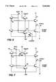
- FIG. 3illustrates the shift register stage of the present invention. This stage is similar to the FIG. 2 stage but with several significant differences.
- First an additional transistor 25is included in the improved stage.
- Transistor 25has its drainsource conduction path coupled between node P1 and a point of reference potential sufficient to turn pull-up transistor 16 off.
- the gate of transistor 25is connected to the output terminal of a subsequent stage. If the present stage is numbered n in a cascade connection of ordinally numbered stages, the gate of transistor 25 is preferably coupled to the output of stage n+2. However, the gate of transistor 25 may be coupled to an other stage, such as stage n+3, with beneficial results.
- Transistor 25will aid in the pull down of node P1 allowing transistor 19 to be smaller in design. In fact the pull down of node P1 may be almost totally under the control of transistor 25 such that the function of transistor 19 may be simply to hold node P1 low once it has been pulled down.
- Transistor 19, being relegated to a hold down functioncan be operated with a lower gate voltage.
- the supply potential applied to the intermediate stagecan therefore be reduced, from for example 16 volts in the FIG. 2 register stage, to about 2 volts in the FIG. 3 register stage.
- This reduction in supply voltage and consequent reduction in gate voltage applied to transistors 19 and 17tends to beneficially lessen the amount of drift in the threshold voltage in transistors 19 and 17. This results in the stage becoming significantly more reliable as well as extending its usable lifetime.
- transistor 17can also be reduced because with the inclusion of transistor 25, it can be assured that a) node P1 will be held low precluding transistor 16 from competing with transistor 17, and b) the safety factor for proper operation is increased due to the stabilizing of the threshold voltage of transistor 17. Note that since transistors 19 and 17 may be reduced in size, transistor 25 may be included without increasing the stage area (in integrated form).
- transistor 18Having the gate and drain electrodes of transistor 18 interconnected conditions transistor 18 to operate as a diode.
- transistor 18may be replaced with a diode.
- Diode connected transistor 18charges node P1 to the input pulse amplitude (minus a threshold value) and transistors 25 and 19 subsequently discharge node P1. Since a diode connected transistor conducts unidirectionally, the potential at node P1 may beneficially be boosted to higher potentials when the clock signal applied to the supply terminal of the output amplifier goes high. That is the gate to drain and gate to source capacitances of pullup transistor 16 will couple a substantial portion of the clock voltage at terminals 14 and 13 to node P1, thereby enhancing the drive capability of transistor 16.
- FIG. 4illustrates a cascade connection of a plurality of stages of the type shown in FIG. 3.
- successive register stagesare driven by different clock phases of a three phase clock C1, C2, C3.
- the output terminal of each successive register stageis coupled to the input terminal of the next register stage.
- the gate electrode of respective transistors 25 of stage nis connected to the output terminal of stage n+2.
- the gate electrode of the respective transistors 25may be coupled to the output terminals of other stages i.e. the gate electrode of transistor 25 of stage n may be connected to the output terminal of stage n+3 etc.
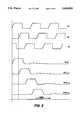
- FIG. 5illustrates voltage-time waveforms for the respective clock phases and selected register stage output terminals. Recall that the output signal of one stage is the input signal for the next stage, hence no unique input signal need be shown.
- the illustrated shift register of FIG. 4is shown utilizing 3-phase clocks, hence 3-phase clocks are included in FIG. 5. It can be seen that after each output terminal outputs the scan pulse, there is a small build up in the output potential only immediately following the scan pulse. This occurs because the transistor 19, having been made smaller, has not completely pulled down node P1, and a portion of the clock phase coupled to the supply terminal of the output stage has leaked through transistor 16. Once transistor 25 has been conditioned to conduct, node P1 is pulled completely down, precluding further leakage of clock pulses through respective transistor 16. Note the FIG. 5 waveforms are generated for the gate electrodes of the respective transistors 25 of respective stages n being connected to the output terminals of respective stages n+3.
- the output pulsesare shown as overlapping.
- the amount of overlapis a function of the amount by which the clock phases overlap.
- the desired output pulse overlapis adjustable for a particular application by adjusting the clock phase overlap.
- FIG. 6illustrates an alternative shift register stage where the control electrode of the clamping transistor 25 is connected to a different one of the clock phases than the one connected to the drain electrode of transistor 16.
- the transistor 25may be connected to the clock phase not connected to transistors 20 and 16.
- the control electrode of transistor 25may be connected to one of the alternative clock phases not connected to transistors 20 and 16.
- the constraint on the clock phase which is connected to the control electrode of the clamping transistor 25is that its pulses occur after both the input signal pulse phase and the clock phase connected to the drain of transistor 16. Connecting the transistor 25 to a clock phase rather than the output connection of a subsequent register stage provides the circuit designer with layout alternatives with respect to integrated circuit topology.
- FIG. 7illustrates a further alternative register stage.
- the source-drain path of the clamping transistor 255is connected between node P1 and the input terminal 12, and its control electrode is connected to clock phase C3.
- the input terminal 12 of an N stage registeris held at a low potential (substantially VSS) at least (N-1)/N th of the time the register is operated, hence the clamping transistor 255 will, when turned on, clamp node P1 low to cut off transistor 16.
- the gate of transistor 255is pulsed every clock cycle insuring that the node P1 is regularly and frequently clamped low.
- the drain electrode of transistor 18may either be connected to a source of constant supply potential, such as VDD, or alternatively it may be connected to the input terminal 12 as shown in FIG. 3.
Landscapes
- Engineering & Computer Science (AREA)
- Chemical & Material Sciences (AREA)
- Crystallography & Structural Chemistry (AREA)
- Physics & Mathematics (AREA)
- Computer Hardware Design (AREA)
- General Physics & Mathematics (AREA)
- Theoretical Computer Science (AREA)
- Liquid Crystal Display Device Control (AREA)
- Shift Register Type Memory (AREA)
- Control Of Indicators Other Than Cathode Ray Tubes (AREA)
Abstract
Description
This is a continuation of application Ser. No. 193,930, filed Feb. 9, 1994, now abandoned, which is a continuation-in-part application of application Ser. No. 08/141,364, filed 28 Oct. 1993, now abandoned.
This invention relates generally to shift registers and particularly to a shift register stage useful as a select line scanner for liquid crystal displays.
Liquid crystal television and computer displays (LCDs) are known in the art. For example, see U.S. Pat. Nos. 4,742,346 and 4,766,430, both issued to G. G. Gillette et al. Displays of the type described in the Gillette patents include a matrix of liquid crystal cells which are arranged at the crossovers of data lines and select lines. The select lines are sequentially selected by a select line scanner to produce the horizontal lines of the display. The data lines apply the brightness (gray scale) signals to the columns of liquid crystal cells as the select lines are sequentially selected.
Preferably, the drive circuitry, which drives the select line scanner, which selects the horizontal lines to be displayed, is fabricated directly onto the same substrate and at the same time as the liquid crystal cells are fabricated. Also, because a large number of data lines and select lines are required for a television or computer display, and because the small pixel pitch limits the space available for laying out the driver circuitry, it is essential to keep the circuitry as simple as possible.
FIG. 1 illustrates an example of a known scan register described in U.S. Pat. No. 5,222,082, which may be integrated with a liquid crystal display device. This register is driven with multiphase clocking signals C1, C2, C3, with different ones of the clock phases applied to different ones of the scan register stages 11.
FIG. 2 illustrates one of the scan register stages in detail. The scan register stage includes an inputsection including transistors section including transistors section including transistors
The output section is arranged as a push-pull amplifier, with a clocked supply potential connected to itssupply connection 14. An output is accessed at the interconnection of thetransistors
The input section is arranged as a switched amplifier to exhibit a predetermined potential during the clock phase applied to the supply terminal of the output section. The output signal, P1, of the input stage, is coupled to drive theoutput transistor 16. More particularly the output, P1, follows the input signal applied to the gate electrode oftransistor 18. The output of the input section will be high when the clock phase applied toterminal 14 goes high, and a high level is translated to theoutput terminal 13. The high level at node P1 is retained at node P1 until the occurrence of a clock phase C3 when the input signal is low. Thus the gate of theoutput transistor 16 will be at a high level when the clock C1 goes high providing a charging path tooutput 13 and when clock C1 goes low, providing a path to discharge theoutput node 13.
The intermediate section is arranged as a clocked inverting amplifier responsive to the input signal. The output of the intermediate stage is coupled to the gate electrode of the pull downtransistor 17 of the output stage. The intermediate stage includes pull up and pull downtransistors transistor 21 is greater than that oftransistor 20 so that if bothtransistors transistor 20 is high when the input signal is high, theoutput transistor 17 will be maintained in a non-conducting state. However since the application of the stage is as a scan register, input signal pulses occur relatively infrequently. As a result node P2 will normally be charged high for every clock pulse of clock phase C3 andoutput transistor 17 will normally be conducting.
The drains oftransistors transistors transistor 19 increases, its ability to discharge node P1 decreases, and more time is required to turn offtransistor 16. The result is that some of the clock C1 voltage may leak onto theoutput node 13 and undesirably affect subsequent register stages as well as erroneously addressing an LCD row of pixels.
The present invention addresses these problems and provides a shift register stage which not only precludes false output values, but also consumes less power.
The present invention is a shift register stage for inclusion in a cascade connection of like stages and to be energized by plural phase clock signals. Adjacent stages of such cascade connection are energized by different combinations of the plural phase clock signals. The shift register stage includes an input circuit and an output stage. The output stage includes a push-pull amplifier comprising pull up and pull down transistors, each having respective control electrodes. The output terminal of the push-pull amplifier is the output terminal for the shift register stage. The input circuit is responsive to a scan pulse applied to its input terminal for generating first and second control signals which are coupled to the control electrodes of the pull-up and pull-down transistors for conditioning the push-pull amplifier to provide output scan pulses. The principal conduction path of a clamp transistor is coupled between the control electrode of the pull up transistor and a source of potential of value sufficient to turn off the pull up transistor. The control electrode of the clamp transistor is connected to an output terminal of a subsequent stage of said cascade connection.
FIG. 1 is a block diagram of a prior art shift register including a plurality of cascaded stages.
FIG. 2 is a schematic diagram of a known shift register stage which may be utilized in the FIG. 1 shift register.
FIG. 3 is a schematic diagram of a shift register stage embodying the present invention.
FIG. 4 is a block diagram of a shift register including a cascade connection of a number of stages illustrated in FIG. 3.
FIG. 5 is a diagram of the relative timing of the output signals and the respective clock signals occurring at respective nodes of the FIGS. 4 shift register utilizing stages illustrated in FIG. 3.
FIGS. 6 and 7 are schematic diagrams of alternative shift register stages embodying the invention.
FIG. 3 illustrates the shift register stage of the present invention. This stage is similar to the FIG. 2 stage but with several significant differences. First anadditional transistor 25 is included in the improved stage.Transistor 25 has its drainsource conduction path coupled between node P1 and a point of reference potential sufficient to turn pull-uptransistor 16 off. The gate oftransistor 25 is connected to the output terminal of a subsequent stage. If the present stage is numbered n in a cascade connection of ordinally numbered stages, the gate oftransistor 25 is preferably coupled to the output of stage n+2. However, the gate oftransistor 25 may be coupled to an other stage, such as stage n+3, with beneficial results.Transistor 25 will aid in the pull down of nodeP1 allowing transistor 19 to be smaller in design. In fact the pull down of node P1 may be almost totally under the control oftransistor 25 such that the function oftransistor 19 may be simply to hold node P1 low once it has been pulled down.
The size oftransistor 17 can also be reduced because with the inclusion oftransistor 25, it can be assured that a) node P1 will be heldlow precluding transistor 16 from competing withtransistor 17, and b) the safety factor for proper operation is increased due to the stabilizing of the threshold voltage oftransistor 17. Note that sincetransistors transistor 25 may be included without increasing the stage area (in integrated form).
An additional change is the elimination of the power supply coupled to the drain electrode oftransistor 18 in the FIG. 2 stage. This supply has been replaced by connecting the drain electrode oftransistor 18 to the input terminal. Since thetransistor 18 draws substantially no source drain current, this connection does not significantly load the output of the preceding cascade connected stage. In addition to eliminating the supply, this change has the further beneficial effect of tending to make the input stage more immune to noise on the input.
Having the gate and drain electrodes oftransistor 18interconnected conditions transistor 18 to operate as a diode. Thus, infact transistor 18 may be replaced with a diode. Diode connectedtransistor 18 charges node P1 to the input pulse amplitude (minus a threshold value) andtransistors pullup transistor 16 will couple a substantial portion of the clock voltage atterminals transistor 16.
FIG. 4 illustrates a cascade connection of a plurality of stages of the type shown in FIG. 3. In the arrangement shown successive register stages are driven by different clock phases of a three phase clock C1, C2, C3. The output terminal of each successive register stage is coupled to the input terminal of the next register stage. The gate electrode ofrespective transistors 25 of stage n is connected to the output terminal ofstage n+ 2. Recall however, that the gate electrode of therespective transistors 25 may be coupled to the output terminals of other stages i.e. the gate electrode oftransistor 25 of stage n may be connected to the output terminal of stage n+3 etc.
FIG. 5 illustrates voltage-time waveforms for the respective clock phases and selected register stage output terminals. Recall that the output signal of one stage is the input signal for the next stage, hence no unique input signal need be shown. The illustrated shift register of FIG. 4 is shown utilizing 3-phase clocks, hence 3-phase clocks are included in FIG. 5. It can be seen that after each output terminal outputs the scan pulse, there is a small build up in the output potential only immediately following the scan pulse. This occurs because thetransistor 19, having been made smaller, has not completely pulled down node P1, and a portion of the clock phase coupled to the supply terminal of the output stage has leaked throughtransistor 16. Oncetransistor 25 has been conditioned to conduct, node P1 is pulled completely down, precluding further leakage of clock pulses throughrespective transistor 16. Note the FIG. 5 waveforms are generated for the gate electrodes of therespective transistors 25 of respective stages n being connected to the output terminals of respective stages n+3.
The output pulses are shown as overlapping. The amount of overlap is a function of the amount by which the clock phases overlap. Thus the desired output pulse overlap is adjustable for a particular application by adjusting the clock phase overlap.
FIG. 6 illustrates an alternative shift register stage where the control electrode of the clampingtransistor 25 is connected to a different one of the clock phases than the one connected to the drain electrode oftransistor 16. In a three phase non-overlapping clocking system, thetransistor 25 may be connected to the clock phase not connected totransistors transistor 25 may be connected to one of the alternative clock phases not connected totransistors transistor 25 is that its pulses occur after both the input signal pulse phase and the clock phase connected to the drain oftransistor 16. Connecting thetransistor 25 to a clock phase rather than the output connection of a subsequent register stage provides the circuit designer with layout alternatives with respect to integrated circuit topology.
FIG. 7 illustrates a further alternative register stage. In this embodiment the source-drain path of the clampingtransistor 255 is connected between node P1 and theinput terminal 12, and its control electrode is connected to clock phase C3. Theinput terminal 12 of an N stage register is held at a low potential (substantially VSS) at least (N-1)/Nth of the time the register is operated, hence the clampingtransistor 255 will, when turned on, clamp node P1 low to cut offtransistor 16. The gate oftransistor 255 is pulsed every clock cycle insuring that the node P1 is regularly and frequently clamped low.
Consider a multiphase clock system where the clocks applied totransistors instance transistor 255 will be pulsed on when the input signal onterminal 12 is high.Transistor 255 will therefore aid in pulling node P1 high, allowingtransistor 18 to be of smaller dimensions. During the clock cycle that an input pulse is applied toterminal 12, the node P1 will be high for the entire clock cycle. However this has no effect on the desired operation of the shift register. Node P1 will be clamped low by the clock C3 during the next clock cycle.
The drain electrode oftransistor 18 may either be connected to a source of constant supply potential, such as VDD, or alternatively it may be connected to theinput terminal 12 as shown in FIG. 3.
Claims (20)
1. A shift register comprising a plurality of substantially identical cascaded stages, each of said stages having an input terminal and an output terminal, said shift register including means for providing a plurality of phase shifted clock signals and means for providing an input signal; said register stages comprising:
an output stage comprising a push-pull amplifier including pull-up and pull-down transistors (16, 17) having respective principal conduction paths connected in series with an interconnection of the pull-up and pull-down transistors forming said register stage output terminal, said push-pull amplifier having a supply terminal (14) for applying one of said plurality of phase shifted clock signals, and said pull-up and pull-down transistors having respective control electrodes;
input circuitry (18-21), responsive to a scan pulse applied to said input terminal (12) for generating first and second control signals which are coupled to the control electrodes of said pull-up and pull-down transistors for conditioning said push-pull amplifier to provide output scan pulses; and
a clamping transistor (25) having a conduction path coupled between the control electrode of the pull up transistor and a source of potential (VSS) of value sufficient to turn off the pull up transistor (16), said clamping transistor having a control electrode coupled to the output terminal of a subsequent one of said cascaded stages.
2. The shift register stage set forth in claim 1 wherein said input circuitry includes first (18) and second (19) transistors having their conduction paths coupled in series with an output terminal (P1) formed at an interconnection of said first and second transistors and coupled to the control electrode of the pull up transistor, said first transistor having a control and first electrode coupled to said input terminal (12) of said input stage, for receiving an input scan pulse.
3. The shift register stage set forth in claim 1 wherein said input circuit further includes third (20) and fourth (21) transistors having their conduction paths coupled in series between supply potentials, with an output terminal (P2) formed at an interconnection of said third (20) and fourth (21) transistors and which is coupled to the control electrode of said pull down transistor and to a control electrode of said second transistor, said third transistor having a control electrode coupled to one of said plurality of phase shifted clock signals, and said fourth transistor having an input terminal coupled to the input terminal (12) of said input stage.
4. The shift register stage set forth in claim 1 wherein said input circuitry includes a diode and a transistor having their conduction paths coupled in series with an output terminal (P1) formed at an interconnection of said diode and transistor and coupled to the control electrode of said pull up transistor, said diode having an electrode coupled to said input terminal of said stage for receiving a scan pulse.
5. A shift register comprising a plurality of substantially identical cascaded stages, each of said stages having an input terminal and an output terminal, said shift register including means for providing a plurality of phase shifted clock signals and means for providing an input signal; said register stages comprising:
an output stage comprising a push-pull amplifier including pull-up (16) and pull-down (17) transistors having respective principal conduction paths connected in series with an interconnection of the pull-up and pull-down transistors forming said register stage output terminal, said push-pull amplifier having a supply terminal (C1) for applying one of said plurality of phase shifted clock signals, and said pull-up and pull-down transistors having respective control electrodes;
an input stage (18, 19) having an output terminal (P1) coupled to the control electrode of said pull-up transistor, and having an input terminal (12) for receiving an input signal, said input stage output terminal following potential changes applied to said input terminal at least for input signal transitions in one direction;
an intermediate stage (20, 21) including a clocked inverting amplifier, having an output terminal (P2) coupled to the control electrode of said pull-down transistor, an input terminal coupled to the input terminal of said register stage, a supply terminal (VDD) for applying supply potential, and a clock input terminal (C3) for applying another of said plurality of phase shifted clock signals, said another of said plurality of phase shifted clock signals selectively activating said inverting amplifier; and
a clamping transistor (25) having a conduction path coupled between the control electrode of the pull up transistor and a source (VSS) of potential of value sufficient to turn off the pull up transistor, said clamping transistor having a control electrode coupled to the output terminal of a subsequent one of said cascaded stages.
6. The shift register stage set forth in claim 5 wherein said input stage includes first and second transistor having their conduction paths coupled in series with said output terminal of said input stage formed at an interconnection of said first and second transistors, said first transistor having a control and first electrode coupled to said input terminal of said input stage, and said second transistor having a control electrode coupled to the output terminal of said intermediate stage.
7. The shift register stage set forth in claim 5 wherein said intermediate stage includes first and second transistor having their conduction paths coupled in series between supply potentials, with said output terminal of said intermediate stage formed at an interconnection of said first and second transistors, said first transistor having a control electrode coupled to said another of said plurality of phase shifted clock signals, and said second transistor having an input terminal coupled to the input terminal of said input stage.
8. The shift register stage set forth in claim 7 wherein said input stage includes third and fourth transistors having respective conduction paths coupled in series with said output terminal of said input stage formed at an interconnection of said third and fourth transistors, said third transistor having a control and first electrode coupled to said input terminal of said input stage, and said fourth transistor having a control electrode coupled to the output terminal of said intermediate stage.
9. The shift register stage set forth in claim 5 wherein said input stage includes a diode and a transistor having their conduction paths coupled in series with said output terminal of said input stage formed at an interconnection of said diode and transistor, said diode having an electrode coupled to said input terminal of said input stage, and said transistor having a control electrode coupled to the output terminal of said intermediate stage.
10. A shift register comprising a plurality of substantially identical cascaded stages, each of said stages having an input terminal and an output terminal, said shift register including means for providing a plurality of phase shifted clock signals and means for providing an input signal; said register stages comprising:
an output stage comprising a push-pull amplifier including pull-up and pull-down transistors having respective principal conduction paths connected in series, with an interconnection of the pull-up and pull-down transistors forming said register stage output terminal, said push-pull amplifier having a supply terminal for applying one of said plurality of phase shifted clock signals, and said pull-up and pull-down transistors having respective control electrodes;
input circuitry, responsive to a scan pulse applied to said input terminal for generating first and second control signals which are coupled to the control electrodes of said pull-up and pull-down transistors for conditioning said push-pull amplifier to provide output scan pulses; and
a clamping transistor having a control electrode and having a conduction path coupled between the control electrode of said pull up transistor and a source of potential, said potential having a value, at least fifty percent of the time during which said register is energized, sufficient to turn off the pull up transistor; and
means for applying a control signal to the control electrode of said clamping transistor, said control signal being substantially out of phase with said one of said plurality of phase shifted clock signals.
11. The shift register set forth is claim 10 wherein said means for applying a control signal to the control electrode of said clamping transistor comprises a connection to another of said plurality of phase shifted clock signals different from said one of said plurality of phase shifted clock signals.
12. The shift register set forth in claim 11 wherein said source of potential comprises a connection to said stage input terminal.
13. The shift register stage set forth in claim 10 wherein said input circuitry includes first and second transistors having their conduction paths coupled in series with an output terminal formed at an interconnection of said first and second transistors and coupled to the control electrode of the pull up transistor, said first transistor having a control and first electrode coupled to said input terminal of said input stage, for receiving an input scan pulse.
14. The shift register stage set forth in claim 10 wherein said input circuit further includes third and fourth transistors having their conduction paths coupled in series between supply potentials, with an output terminal formed at an interconnection of said third and fourth transistors and which is coupled to the control electrode of said pull down transistor and to a control electrode of said second transistor, said third transistor having a control electrode coupled to one of said plurality of phase shifted clock signals, and said fourth transistor having an input terminal coupled to the input terminal of said input stage.
15. The shift register stage set forth in claim 10 wherein said input circuitry includes a diode and a transistor having their conduction paths coupled in series with an output terminal (P1) formed at an interconnection of said diode and transistor and coupled to the control electrode of said pull up transistor, said diode having an electrode coupled to said input terminal of said stage for receiving a scan pulse.
16. A shift register comprising a plurality of substantially identical cascaded stages, each of said stages having an input terminal and an output terminal, said shift register including means for providing a plurality of phase shifted clock signals and means for providing an input signal; said register stages comprising:
an output section comprising a pull-up transistor having a principal conduction path connected in series with a DC impedance, and wherein an interconnection of the pull-up transistor and the DC impedance constitutes said register stage output terminal, said output section having a supply terminal for applying one of said plurality of phase shifted clock signals to the principal conduction path of said pull-up transistor, and said pull-up transistor having a control electrode;
input circuitry including a clamping transistor, said input circuitry responsive to a scan pulse applied to said input terminal of said stage for generating a control signal which is coupled to the control electrode of said pull-up transistor for conditioning said output section to provide output scan pulses, and said clamping transistor having a principal conduction path coupled between the control electrode of said pull up transistor and a source of potential sufficient to turn off said pull up transistor and having a control electrode coupled to an output terminal of a subsequent stage of said cascaded stages.
17. The shift register stage set forth in claim 16 wherein said input circuitry includes a diode and said clamping transistor having respective principal conduction paths coupled in series with an output terminal (P1) formed at an interconnection of said diode and clamping transistor and coupled to the control electrode of said pull up transistor, said diode having an electrode coupled to said input terminal of said stage for receiving a scan pulse.
18. The shift register stage set forth in claim 16 wherein said input circuitry includes a first transistor and said clamping transistor having respective principal conduction paths coupled in series with an output terminal formed at an interconnection of said first and clamping transistors and coupled to the control electrode of the pull up transistor, said first transistor having at least a control electrode coupled to said input terminal of said input stage, for receiving an input scan pulse.
19. The shift register stage set forth in claim 16 wherein said DC impedance is a transistor having a principal conduction path in series with the principal conduction path of said pull-up transistor, and having a control electrode, and;
circuitry for applying to said control electrode of said transistor, for at least a portion of at least one period of said phase shifted clock signals, a potential of sufficient magnitude to condition said transistor into conduction.
20. The shift register stage set forth in claim 16 wherein said circuitry for applying a potential of sufficient magnitude to condition said transistor into conduction comprises:
an inverting amplifier having an input terminal coupled to the input terminal of said stage and an output terminal coupled to the control electrode of said transistor.
Priority Applications (2)
| Application Number | Priority Date | Filing Date | Title |
|---|---|---|---|
| US08/289,324US5410583A (en) | 1993-10-28 | 1994-08-11 | Shift register useful as a select line scanner for a liquid crystal display |
| CZ19942516ACZ287534B6 (en) | 1993-10-28 | 1994-10-12 | Shift register useful particularly as a select line scanner for a liquid crystal display |
Applications Claiming Priority (3)
| Application Number | Priority Date | Filing Date | Title |
|---|---|---|---|
| US14136493A | 1993-10-28 | 1993-10-28 | |
| US19393094A | 1994-02-09 | 1994-02-09 | |
| US08/289,324US5410583A (en) | 1993-10-28 | 1994-08-11 | Shift register useful as a select line scanner for a liquid crystal display |
Related Parent Applications (1)
| Application Number | Title | Priority Date | Filing Date |
|---|---|---|---|
| US19393094AContinuation | 1993-10-28 | 1994-02-09 |
Publications (1)
| Publication Number | Publication Date |
|---|---|
| US5410583Atrue US5410583A (en) | 1995-04-25 |
Family
ID=26839036
Family Applications (1)
| Application Number | Title | Priority Date | Filing Date |
|---|---|---|---|
| US08/289,324Expired - LifetimeUS5410583A (en) | 1993-10-28 | 1994-08-11 | Shift register useful as a select line scanner for a liquid crystal display |
Country Status (12)
| Country | Link |
|---|---|
| US (1) | US5410583A (en) |
| EP (1) | EP0651395B1 (en) |
| JP (1) | JP4034362B2 (en) |
| KR (1) | KR100317408B1 (en) |
| CN (1) | CN1049755C (en) |
| DE (1) | DE69420667T2 (en) |
| ES (1) | ES2135519T3 (en) |
| MY (1) | MY119362A (en) |
| RU (1) | RU2116678C1 (en) |
| SG (1) | SG87733A1 (en) |
| TR (1) | TR28054A (en) |
| TW (1) | TW355782B (en) |
Cited By (89)
| Publication number | Priority date | Publication date | Assignee | Title |
|---|---|---|---|---|
| US5517542A (en)* | 1995-03-06 | 1996-05-14 | Thomson Consumer Electronics, S.A. | Shift register with a transistor operating in a low duty cycle |
| US5701136A (en)* | 1995-03-06 | 1997-12-23 | Thomson Consumer Electronics S.A. | Liquid crystal display driver with threshold voltage drift compensation |
| US5859630A (en)* | 1996-12-09 | 1999-01-12 | Thomson Multimedia S.A. | Bi-directional shift register |
| US5949398A (en)* | 1996-04-12 | 1999-09-07 | Thomson Multimedia S.A. | Select line driver for a display matrix with toggling backplane |
| US6052426A (en)* | 1994-05-17 | 2000-04-18 | Thomson Lcd | Shift register using M.I.S. transistors of like polarity |
| US6295046B1 (en)* | 1997-09-03 | 2001-09-25 | Lg Philips Lcd Co., Ltd. | Shift register unit and display device |
| US6300928B1 (en) | 1997-08-09 | 2001-10-09 | Lg Electronics Inc. | Scanning circuit for driving liquid crystal display |
| US6426743B1 (en)* | 1999-02-09 | 2002-07-30 | Lg. Philips Lcd Co., Ltd | Shift register |
| US6437596B1 (en) | 1999-01-28 | 2002-08-20 | International Business Machines Corporation | Integrated circuits for testing a display array |
| US6448954B1 (en)* | 1995-11-06 | 2002-09-10 | Semiconductor Energy Laboratory Co., Ltd. | Active matrix display device and scanning circuit |
| US20030002615A1 (en)* | 2001-06-29 | 2003-01-02 | Casio Computer Co., Ltd. | Shift register and electronic apparatus |
| US6630920B1 (en)* | 1998-04-07 | 2003-10-07 | Sony Corporation | Pel drive circuit, combination pel-drive-circuit/pel-integrated device, and liquid crystal display device |
| US20030210220A1 (en)* | 2002-05-10 | 2003-11-13 | Alps Electric Co., Ltd. | Shift register apparatus and display apparatus |
| KR100415618B1 (en)* | 2001-12-26 | 2004-01-24 | 엘지.필립스 엘시디 주식회사 | Shift Register |
| US20040263439A1 (en)* | 2003-06-30 | 2004-12-30 | Sanyo Electric Co., Ltd. | Display |
| US20050083292A1 (en)* | 2002-06-15 | 2005-04-21 | Seung-Hwan Moon | Method of driving a shift register, a shift register, a liquid crystal display device having the shift register |
| US6919874B1 (en) | 1994-05-17 | 2005-07-19 | Thales Avionics Lcd S.A. | Shift register using M.I.S. transistors and supplementary column |
| US6940300B1 (en) | 1998-09-23 | 2005-09-06 | International Business Machines Corporation | Integrated circuits for testing an active matrix display array |
| US20050264505A1 (en)* | 2004-05-27 | 2005-12-01 | Lg Philips Lcd Co., Ltd. | Shift register and liquid crystal display device using the same |
| US20050285840A1 (en)* | 2004-06-29 | 2005-12-29 | Yong-Ho Jang | Driving circuit including shift register and flat panel display device using the same |
| US20060001637A1 (en)* | 2004-06-30 | 2006-01-05 | Sang-Jin Pak | Shift register, display device having the same and method of driving the same |
| US20060022920A1 (en)* | 2004-07-28 | 2006-02-02 | Lg.Philips Lcd Co., Ltd. | Display device and driving method thereof |
| US20060044247A1 (en)* | 2004-08-31 | 2006-03-02 | Lg. Philips Lcd Co. Ltd. | Built-in gate driver and display device having the same |
| US20060061535A1 (en)* | 2004-09-23 | 2006-03-23 | Lg Philips Lcd Co., Ltd. | Liquid crystal display device and method of driving the same |
| US20060145998A1 (en)* | 2004-12-31 | 2006-07-06 | Lg. Philips Lcd Co., Ltd. | Driving unit for liquid crystal display device |
| US20060256066A1 (en)* | 2002-06-10 | 2006-11-16 | Seung-Hwan Moon | Shift register, liquid crystal display device having the shift register and method of driving scan lines using the same |
| US20060262588A1 (en)* | 2005-04-05 | 2006-11-23 | Stmicroelectronics Sa | Memory circuit containing a chain of stages |
| US20060267911A1 (en)* | 2005-05-26 | 2006-11-30 | Lg.Philips Lcd Co., Ltd. | Shift register and display device using the same and driving method thereof |
| US20070035505A1 (en)* | 2005-08-11 | 2007-02-15 | Au Optronics Corp. | Shift register circuit |
| US20070046327A1 (en)* | 2005-08-25 | 2007-03-01 | Au Optronics Corp. | Shift register circuit |
| US20070085809A1 (en)* | 2005-10-18 | 2007-04-19 | Au Optronics Corporation | Backup shift register module for a gateline driving circuit |
| KR100722124B1 (en) | 2005-08-29 | 2007-05-25 | 삼성에스디아이 주식회사 | Scan Driving Circuit and Organic Electroluminescent Device Using the Same |
| US20070245193A1 (en)* | 2006-03-22 | 2007-10-18 | Au Optronics Corp. | Liquid crystal display and shift register unit thereof |
| CN100362593C (en)* | 2003-01-25 | 2008-01-16 | 夏普株式会社 | Shift Register |
| KR100803163B1 (en)* | 2001-09-03 | 2008-02-14 | 삼성전자주식회사 | LCD Display |
| US20080042962A1 (en)* | 2006-08-21 | 2008-02-21 | Au Optronics Corporation | Display and display panel thereof |
| US20080055293A1 (en)* | 2006-09-01 | 2008-03-06 | Au Optronics Corp. | Signal-driving system and shift register unit thereof |
| US20080079682A1 (en)* | 2006-09-01 | 2008-04-03 | Au Optronics Corp. | Control circuit for releasing residual charges |
| US20080088564A1 (en)* | 2006-10-17 | 2008-04-17 | Au Optronics Corporation | Driving Circuit of Liquid Crystal Display |
| CN100403385C (en)* | 2001-02-13 | 2008-07-16 | 三星电子株式会社 | Shift register and liquid crystal display using shift register |
| US20080174580A1 (en)* | 2006-10-13 | 2008-07-24 | Au Optronics Corporation | Gate Driver and Driving Method Thereof in Liquid Crystal Display |
| US20080191994A1 (en)* | 2007-02-09 | 2008-08-14 | Innolux Display Corp. | Shift register with no overlap effective output signal and liquid crystal display using the same |
| US20080192883A1 (en)* | 2007-02-09 | 2008-08-14 | Innolux Display Corp. | Shift register with six transistors and liquid crystal display using the same |
| US20080191993A1 (en)* | 2007-02-09 | 2008-08-14 | Innolux Display Corp. | Shift register with lower power consumption and liquid crystal display using the same |
| US20080279327A1 (en)* | 2007-05-09 | 2008-11-13 | Chunghwa Picture Tubes, Ltd. | Shift register and shift register apparatus thereof |
| CN100489932C (en)* | 2006-01-17 | 2009-05-20 | 奇晶光电股份有限公司 | Flat panel display, display driving device and shift register |
| US20090129495A1 (en)* | 2004-06-25 | 2009-05-21 | Yongseok Jin | Allocation of radio resource in orthogonal frequency division multiplexing system |
| CN100495576C (en)* | 2005-09-07 | 2009-06-03 | 友达光电股份有限公司 | shift register circuit |
| CN100514403C (en)* | 2006-01-17 | 2009-07-15 | 奇晶光电股份有限公司 | Shift temporary storage device |
| CN100520895C (en)* | 2006-02-07 | 2009-07-29 | 友达光电股份有限公司 | Shift register for starting feedback circuit according to next-stage signal |
| US20090189677A1 (en)* | 2008-01-25 | 2009-07-30 | Samsung Electronics Co., Ltd | Gate driving circuit and display apparatus having the same |
| US20090213982A1 (en)* | 2008-02-21 | 2009-08-27 | Hsin-Wei Peng | Shift register and liquid crystal display (lcd) |
| US20100054392A1 (en)* | 2008-08-27 | 2010-03-04 | Au Optronics Corp. | Shift register |
| KR100962660B1 (en) | 2003-05-31 | 2010-06-11 | 삼성전자주식회사 | Gate driving circuit |
| US20100201659A1 (en)* | 2009-02-12 | 2010-08-12 | Semiconductor Energy Laboratory Co., Ltd. | Pulse output circuit, display device, and electronic device |
| CN101339810B (en)* | 2007-07-06 | 2010-08-25 | 群康科技(深圳)有限公司 | Shift register and LCD device using the same |
| US20100226473A1 (en)* | 2009-03-05 | 2010-09-09 | Au Optronics Corp. | Shift register |
| US20100246750A1 (en)* | 2009-03-26 | 2010-09-30 | Semiconductor Energy Laboratory Co., Ltd. | Semiconductor Device and Electronic Device Including Semiconductor Device |
| US20100245335A1 (en)* | 2009-03-26 | 2010-09-30 | Semiconductor Energy Laboratory Co., Ltd. | Liquid crystal display device, driving method of the same, and electronic device including the same |
| US20100245307A1 (en)* | 2009-03-26 | 2010-09-30 | Semiconductor Energy Laboratory Co., Ltd. | Liquid Crystal Display Device and Electronic Device Including the Same |
| US7831010B2 (en) | 2007-11-12 | 2010-11-09 | Mitsubishi Electric Corporation | Shift register circuit |
| US20100315403A1 (en)* | 2008-02-19 | 2010-12-16 | Shotaro Kaneyoshi | Display device, method for driving the display device, and scan signal line driving circuit |
| US20100321372A1 (en)* | 2008-02-19 | 2010-12-23 | Akihisa Iwamoto | Display device and method for driving display |
| US20110001732A1 (en)* | 2008-02-19 | 2011-01-06 | Hideki Morii | Shift register circuit, display device, and method for driving shift register circuit |
| US20110033022A1 (en)* | 2008-04-29 | 2011-02-10 | Patrick Zebedee | Digital logic circuit, shift register and active matrix device |
| US7949085B2 (en) | 2006-06-29 | 2011-05-24 | Au Optronics Corp. | Stressless shift register |
| US20110193832A1 (en)* | 2010-02-09 | 2011-08-11 | Sony Corporation | Display device and electronic apparatus |
| US20110193622A1 (en)* | 2006-10-17 | 2011-08-11 | Semiconductor Energy Laboratory Co., Ltd. | Pulse output circuit, shift register, and display device |
| US20110193853A1 (en)* | 2008-11-28 | 2011-08-11 | Sharp Kabushiki Kaisha | Scanning signal line drive circuit, shift register and display device |
| US20110199354A1 (en)* | 2008-12-10 | 2011-08-18 | Yasuaki Iwase | Scanning signal line drive circuit, shift register, and drive method of shift register |
| US20110234565A1 (en)* | 2008-12-12 | 2011-09-29 | Sharp Kabushiki Kaisha | Shift register circuit, display device, and method for driving shift register circuit |
| US20120013588A1 (en)* | 2010-07-19 | 2012-01-19 | Samsung Mobile Display Co., Ltd. | Display, Scan Driving Apparatus for the Display, and Driving Method Thereof |
| US20120188210A1 (en)* | 2010-02-08 | 2012-07-26 | Peking University Shenzhen Graduate School | Gate driving circuit unit, gate driving circuit and display device |
| US20130177128A1 (en)* | 2012-01-11 | 2013-07-11 | Hannstar Display Corp. | Shift register and method thereof |
| CN103500561A (en)* | 2013-10-12 | 2014-01-08 | 昆山龙腾光电有限公司 | Gate driving circuit |
| TWI460735B (en)* | 2006-06-02 | 2014-11-11 | Semiconductor Energy Lab | Liquid crystal display device and electronic device |
| TWI488187B (en)* | 2012-11-30 | 2015-06-11 | Au Optronics Corp | Shift register and display apparatus |
| US9153341B2 (en) | 2005-10-18 | 2015-10-06 | Semiconductor Energy Laboratory Co., Ltd. | Shift register, semiconductor device, display device, and electronic device |
| US9171842B2 (en) | 2012-07-30 | 2015-10-27 | Semiconductor Energy Laboratory Co., Ltd. | Sequential circuit and semiconductor device |
| US9406699B2 (en) | 2006-01-07 | 2016-08-02 | Semiconductor Energy Laboratory Co., Ltd. | Semiconductor device, and display device and electronic device having the same |
| US20160240159A1 (en)* | 2013-10-08 | 2016-08-18 | Sharp Kabushiki Kaisha | Shift register and display device |
| US9842861B2 (en) | 2006-09-29 | 2017-12-12 | Semiconductor Energy Laboratory Co., Ltd. | Display device |
| US9881688B2 (en) | 2012-10-05 | 2018-01-30 | Sharp Kabushiki Kaisha | Shift register |
| US9959822B2 (en) | 2009-10-16 | 2018-05-01 | Semiconductor Energy Laboratory Co., Ltd. | Liquid crystal display device and electronic device including the liquid crystal display device |
| US20180174503A1 (en)* | 2016-12-19 | 2018-06-21 | Lg Display Co., Ltd. | Gate driving circuit |
| CN112233622A (en)* | 2020-10-22 | 2021-01-15 | 深圳市华星光电半导体显示技术有限公司 | GOA circuit and display panel |
| US11296120B2 (en) | 2009-10-09 | 2022-04-05 | Semiconductor Energy Laboratory Co., Ltd. | Shift register and display device and driving method thereof |
| US11348653B2 (en) | 2010-03-02 | 2022-05-31 | Semiconductor Energy Laboratory Co., Ltd. | Pulse signal output circuit and shift register |
| US11545105B2 (en) | 2009-09-16 | 2023-01-03 | Semiconductor Energy Laboratory Co., Ltd. | Semiconductor device and electronic appliance |
Families Citing this family (54)
| Publication number | Priority date | Publication date | Assignee | Title |
|---|---|---|---|---|
| DE19950860B4 (en)* | 1998-10-21 | 2009-08-27 | Lg Display Co., Ltd. | shift register |
| JP3777894B2 (en)* | 1999-08-06 | 2006-05-24 | カシオ計算機株式会社 | Shift register and electronic device |
| JP3809750B2 (en)* | 1999-12-02 | 2006-08-16 | カシオ計算機株式会社 | Shift register and electronic device |
| JP4761643B2 (en)* | 2001-04-13 | 2011-08-31 | 東芝モバイルディスプレイ株式会社 | Shift register, drive circuit, electrode substrate, and flat display device |
| KR100830903B1 (en)* | 2001-12-27 | 2008-05-22 | 삼성전자주식회사 | Shift register and liquid crystal display device having same |
| JP4302535B2 (en)* | 2002-04-08 | 2009-07-29 | サムスン エレクトロニクス カンパニー リミテッド | Gate driving circuit and liquid crystal display device having the same |
| KR100860239B1 (en)* | 2002-04-08 | 2008-09-25 | 삼성전자주식회사 | Liquid crystal display apparatus |
| KR100863502B1 (en)* | 2002-07-02 | 2008-10-15 | 삼성전자주식회사 | Shift register and liquid crystal display having the same |
| TWI309831B (en)* | 2002-09-25 | 2009-05-11 | Semiconductor Energy Lab | Clocked inverter, nand, nor and shift register |
| KR100910562B1 (en) | 2002-12-17 | 2009-08-03 | 삼성전자주식회사 | Drive of display device |
| US7319452B2 (en)* | 2003-03-25 | 2008-01-15 | Samsung Electronics Co., Ltd. | Shift register and display device having the same |
| KR101022293B1 (en)* | 2003-03-25 | 2011-03-21 | 삼성전자주식회사 | Shift register and display device having same |
| CN100358052C (en)* | 2003-04-04 | 2007-12-26 | 胜华科技股份有限公司 | Shift register |
| CN100359607C (en)* | 2003-06-04 | 2008-01-02 | 友达光电股份有限公司 | shift register circuit |
| JP4535696B2 (en)* | 2003-06-27 | 2010-09-01 | 三洋電機株式会社 | Display device |
| JP4565816B2 (en)* | 2003-06-30 | 2010-10-20 | 三洋電機株式会社 | Display device |
| US7289594B2 (en) | 2004-03-31 | 2007-10-30 | Lg.Philips Lcd Co., Ltd. | Shift registrer and driving method thereof |
| KR101053207B1 (en)* | 2004-10-06 | 2011-08-01 | 엘지디스플레이 주식회사 | Shift register and stage circuit for liquid crystal display device for overlap driving |
| KR101055208B1 (en)* | 2004-11-11 | 2011-08-08 | 엘지디스플레이 주식회사 | Shift register |
| KR101055207B1 (en)* | 2004-11-11 | 2011-08-08 | 엘지디스플레이 주식회사 | Shift register |
| JP4794158B2 (en)* | 2004-11-25 | 2011-10-19 | 三洋電機株式会社 | Display device |
| KR101078454B1 (en)* | 2004-12-31 | 2011-10-31 | 엘지디스플레이 주식회사 | Shift register without noises and liquid crystal display device having thereof |
| KR101143004B1 (en)* | 2005-06-13 | 2012-05-11 | 삼성전자주식회사 | Shift register and display device including shifter register |
| KR101183431B1 (en)* | 2005-06-23 | 2012-09-14 | 엘지디스플레이 주식회사 | Gate driver |
| KR100714003B1 (en)* | 2005-08-22 | 2007-05-04 | 삼성에스디아이 주식회사 | Shift register circuit |
| KR101308440B1 (en)* | 2005-10-27 | 2013-09-16 | 엘지디스플레이 주식회사 | A shift register |
| JP2006120308A (en)* | 2005-10-28 | 2006-05-11 | Casio Comput Co Ltd | Shift register and electronic apparatus |
| JP4654923B2 (en)* | 2006-01-26 | 2011-03-23 | カシオ計算機株式会社 | Shift register circuit and display driving device |
| CN100547416C (en)* | 2006-03-16 | 2009-10-07 | 统宝光电股份有限公司 | Scanning detection device and method for flat panel display |
| KR100776510B1 (en)* | 2006-04-18 | 2007-11-16 | 삼성에스디아이 주식회사 | Scan driving circuit and organic light emitting display device using same |
| JP2007317288A (en)* | 2006-05-25 | 2007-12-06 | Mitsubishi Electric Corp | Shift register circuit and image display apparatus including the same |
| TWI366814B (en)* | 2006-07-12 | 2012-06-21 | Wintek Corp | Shift register |
| CN100463042C (en)* | 2006-09-27 | 2009-02-18 | 友达光电股份有限公司 | Control circuit capable of eliminating residual charge |
| JP5525685B2 (en)* | 2006-10-17 | 2014-06-18 | 株式会社半導体エネルギー研究所 | Semiconductor device and electronic equipment |
| CN100426067C (en)* | 2006-11-14 | 2008-10-15 | 友达光电股份有限公司 | Driving circuit of liquid crystal display device |
| JP2008140489A (en)* | 2006-12-04 | 2008-06-19 | Seiko Epson Corp | Shift register, scanning line driving circuit, data line driving circuit, electro-optical device, and electronic apparatus |
| KR101351375B1 (en)* | 2006-12-27 | 2014-01-14 | 엘지디스플레이 주식회사 | A shift register |
| JP4968681B2 (en)* | 2007-07-17 | 2012-07-04 | Nltテクノロジー株式会社 | Semiconductor circuit, display device using the same, and driving method thereof |
| CN101377956B (en)* | 2007-08-31 | 2010-12-29 | 群康科技(深圳)有限公司 | Shift register and LCD |
| CN101388253B (en)* | 2007-09-14 | 2011-07-27 | 群康科技(深圳)有限公司 | Shifting register and LCD |
| CN101527170B (en)* | 2008-03-03 | 2011-05-11 | 中华映管股份有限公司 | Shift register and liquid crystal display |
| JP5472781B2 (en)* | 2008-10-08 | 2014-04-16 | Nltテクノロジー株式会社 | Shift register, display device, and shift register driving method |
| BRPI1013283A2 (en)* | 2009-06-15 | 2019-04-09 | Sharp Kk | shift log and display device |
| JP5209117B2 (en)* | 2009-06-17 | 2013-06-12 | シャープ株式会社 | Flip-flop, shift register, display drive circuit, display device, display panel |
| WO2010150574A1 (en)* | 2009-06-25 | 2010-12-29 | シャープ株式会社 | Shift register circuit, display device provided with same, and shift register circuit driving method |
| JP5208277B2 (en)* | 2009-07-15 | 2013-06-12 | シャープ株式会社 | Scanning signal line driving circuit and display device including the same |
| CN102598145B (en)* | 2009-11-04 | 2013-10-30 | 夏普株式会社 | Shift register and scanning signal line driving circuit provided there with, and display device |
| JP5132818B2 (en)* | 2009-12-15 | 2013-01-30 | シャープ株式会社 | Scanning signal line driving circuit and display device including the same |
| KR101373979B1 (en)* | 2010-05-07 | 2014-03-14 | 엘지디스플레이 주식회사 | Gate shift register and display device using the same |
| CN102479552B (en)* | 2010-11-25 | 2015-11-18 | 上海天马微电子有限公司 | PMOS dynamic shift register unit and dynamic shift register |
| RU2486611C1 (en)* | 2011-11-11 | 2013-06-27 | Открытое акционерное общество "Научно-производственный центр "Полюс" | Redundant register in multi-phase code |
| TWI460699B (en)* | 2012-04-06 | 2014-11-11 | Innocom Tech Shenzhen Co Ltd | Image display system and bi-directional shift register circuit |
| JP6159004B2 (en)* | 2016-11-21 | 2017-07-05 | 株式会社半導体エネルギー研究所 | Semiconductor device |
| US12205530B2 (en) | 2022-09-26 | 2025-01-21 | Beijing Boe Optoelectronics Technology Co., Ltd. | Scan circuit and display apparatus |
Citations (4)
| Publication number | Priority date | Publication date | Assignee | Title |
|---|---|---|---|---|
| US5055720A (en)* | 1990-08-31 | 1991-10-08 | Simtek Corporation | Current mirror sense amplifier with reduced current consumption and enhanced output signal |
| US5055709A (en)* | 1990-04-30 | 1991-10-08 | Motorola, Inc. | DCFL latch having a shared load |
| US5222082A (en)* | 1991-02-28 | 1993-06-22 | Thomson Consumer Electronics, S.A. | Shift register useful as a select line scanner for liquid crystal display |
| US5300822A (en)* | 1991-12-25 | 1994-04-05 | Nec Corporation | Power-on-reset circuit |
Family Cites Families (9)
| Publication number | Priority date | Publication date | Assignee | Title |
|---|---|---|---|---|
| GB1459951A (en)* | 1974-07-25 | 1976-12-31 | Integrated Photomatrix Ltd | Shift registers |
| JPS58181321A (en)* | 1982-04-16 | 1983-10-24 | Hitachi Ltd | Solid-state scanning circuit |
| JPS5945696A (en)* | 1982-09-08 | 1984-03-14 | Sony Corp | Signal transmitting circuit |
| US4496857A (en)* | 1982-11-01 | 1985-01-29 | International Business Machines Corporation | High speed low power MOS buffer circuit for converting TTL logic signal levels to MOS logic signal levels |
| SU1269210A1 (en)* | 1985-04-01 | 1986-11-07 | Предприятие П/Я В-2892 | Shift register based on insulated-gate field-effect transistors |
| US4766430A (en)* | 1986-12-19 | 1988-08-23 | General Electric Company | Display device drive circuit |
| US4958085A (en)* | 1987-10-30 | 1990-09-18 | Canon Kabushiki Kaisha | Scanning circuit outputting scanning pulse signals of two or more phases |
| US5136622A (en)* | 1991-02-28 | 1992-08-04 | Thomson, S.A. | Shift register, particularly for a liquid crystal display |
| JPH0583377A (en)* | 1991-09-25 | 1993-04-02 | Nec Corp | Subscriber line testing system |
- 1994
- 1994-08-11USUS08/289,324patent/US5410583A/ennot_activeExpired - Lifetime
- 1994-10-13TWTW083109508Apatent/TW355782B/ennot_activeIP Right Cessation
- 1994-10-19ESES94116460Tpatent/ES2135519T3/ennot_activeExpired - Lifetime
- 1994-10-19SGSG9602599Apatent/SG87733A1/enunknown
- 1994-10-19EPEP94116460Apatent/EP0651395B1/ennot_activeExpired - Lifetime
- 1994-10-19DEDE69420667Tpatent/DE69420667T2/ennot_activeExpired - Lifetime
- 1994-10-25KRKR1019940027251Apatent/KR100317408B1/ennot_activeExpired - Lifetime
- 1994-10-27JPJP26421994Apatent/JP4034362B2/ennot_activeExpired - Fee Related
- 1994-10-27RURU94039290Apatent/RU2116678C1/enactive
- 1994-10-27CNCN94113666Apatent/CN1049755C/ennot_activeExpired - Lifetime
- 1994-10-28TRTR01130/94Apatent/TR28054A/enunknown
- 1994-10-28MYMYPI94002870Apatent/MY119362A/enunknown
Patent Citations (4)
| Publication number | Priority date | Publication date | Assignee | Title |
|---|---|---|---|---|
| US5055709A (en)* | 1990-04-30 | 1991-10-08 | Motorola, Inc. | DCFL latch having a shared load |
| US5055720A (en)* | 1990-08-31 | 1991-10-08 | Simtek Corporation | Current mirror sense amplifier with reduced current consumption and enhanced output signal |
| US5222082A (en)* | 1991-02-28 | 1993-06-22 | Thomson Consumer Electronics, S.A. | Shift register useful as a select line scanner for liquid crystal display |
| US5300822A (en)* | 1991-12-25 | 1994-04-05 | Nec Corporation | Power-on-reset circuit |
Cited By (178)
| Publication number | Priority date | Publication date | Assignee | Title |
|---|---|---|---|---|
| US6919874B1 (en) | 1994-05-17 | 2005-07-19 | Thales Avionics Lcd S.A. | Shift register using M.I.S. transistors and supplementary column |
| US6052426A (en)* | 1994-05-17 | 2000-04-18 | Thomson Lcd | Shift register using M.I.S. transistors of like polarity |
| US5701136A (en)* | 1995-03-06 | 1997-12-23 | Thomson Consumer Electronics S.A. | Liquid crystal display driver with threshold voltage drift compensation |
| US5517542A (en)* | 1995-03-06 | 1996-05-14 | Thomson Consumer Electronics, S.A. | Shift register with a transistor operating in a low duty cycle |
| US6448954B1 (en)* | 1995-11-06 | 2002-09-10 | Semiconductor Energy Laboratory Co., Ltd. | Active matrix display device and scanning circuit |
| US6741231B2 (en)* | 1995-11-06 | 2004-05-25 | Semiconductor Energy Laboratory Co., Ltd. | Active matrix display device and scanning circuit |
| US5949398A (en)* | 1996-04-12 | 1999-09-07 | Thomson Multimedia S.A. | Select line driver for a display matrix with toggling backplane |
| KR100430314B1 (en)* | 1996-04-12 | 2004-07-15 | 톰슨 | Select line drive for a display matrix with toggling backplane |
| US5859630A (en)* | 1996-12-09 | 1999-01-12 | Thomson Multimedia S.A. | Bi-directional shift register |
| US6300928B1 (en) | 1997-08-09 | 2001-10-09 | Lg Electronics Inc. | Scanning circuit for driving liquid crystal display |
| US6295046B1 (en)* | 1997-09-03 | 2001-09-25 | Lg Philips Lcd Co., Ltd. | Shift register unit and display device |
| US6630920B1 (en)* | 1998-04-07 | 2003-10-07 | Sony Corporation | Pel drive circuit, combination pel-drive-circuit/pel-integrated device, and liquid crystal display device |
| US6940300B1 (en) | 1998-09-23 | 2005-09-06 | International Business Machines Corporation | Integrated circuits for testing an active matrix display array |
| US6437596B1 (en) | 1999-01-28 | 2002-08-20 | International Business Machines Corporation | Integrated circuits for testing a display array |
| US6426743B1 (en)* | 1999-02-09 | 2002-07-30 | Lg. Philips Lcd Co., Ltd | Shift register |
| CN100403385C (en)* | 2001-02-13 | 2008-07-16 | 三星电子株式会社 | Shift register and liquid crystal display using shift register |
| US20030002615A1 (en)* | 2001-06-29 | 2003-01-02 | Casio Computer Co., Ltd. | Shift register and electronic apparatus |
| US6876353B2 (en)* | 2001-06-29 | 2005-04-05 | Casio Computer Co., Ltd. | Shift register and electronic apparatus |
| KR100803163B1 (en)* | 2001-09-03 | 2008-02-14 | 삼성전자주식회사 | LCD Display |
| KR100415618B1 (en)* | 2001-12-26 | 2004-01-24 | 엘지.필립스 엘시디 주식회사 | Shift Register |
| US20030210220A1 (en)* | 2002-05-10 | 2003-11-13 | Alps Electric Co., Ltd. | Shift register apparatus and display apparatus |
| US20060256066A1 (en)* | 2002-06-10 | 2006-11-16 | Seung-Hwan Moon | Shift register, liquid crystal display device having the shift register and method of driving scan lines using the same |
| US8866724B2 (en)* | 2002-06-10 | 2014-10-21 | Samsung Display Co., Ltd. | Shift register, liquid crystal display device having the shift register and method of driving scan lines using the same |
| US7696974B2 (en)* | 2002-06-15 | 2010-04-13 | Samsung Electronics Co., Ltd. | Method of driving a shift register, a shift register, a liquid crystal display device having the shift register |
| US20050083292A1 (en)* | 2002-06-15 | 2005-04-21 | Seung-Hwan Moon | Method of driving a shift register, a shift register, a liquid crystal display device having the shift register |
| CN100362593C (en)* | 2003-01-25 | 2008-01-16 | 夏普株式会社 | Shift Register |
| KR100962660B1 (en) | 2003-05-31 | 2010-06-11 | 삼성전자주식회사 | Gate driving circuit |
| US7474284B2 (en)* | 2003-06-30 | 2009-01-06 | Sanyo Electric Co., Ltd. | Shift register for driving display |
| US20040263439A1 (en)* | 2003-06-30 | 2004-12-30 | Sanyo Electric Co., Ltd. | Display |
| US20050264505A1 (en)* | 2004-05-27 | 2005-12-01 | Lg Philips Lcd Co., Ltd. | Shift register and liquid crystal display device using the same |
| US9135878B2 (en)* | 2004-05-27 | 2015-09-15 | Lg Display Co., Ltd. | Shift register and liquid crystal display device using the same |
| US8027243B2 (en)* | 2004-06-25 | 2011-09-27 | Lg Electronics Inc. | Allocation of radio resource in orthogonal frequency division multiplexing system |
| US20090129495A1 (en)* | 2004-06-25 | 2009-05-21 | Yongseok Jin | Allocation of radio resource in orthogonal frequency division multiplexing system |
| US20050285840A1 (en)* | 2004-06-29 | 2005-12-29 | Yong-Ho Jang | Driving circuit including shift register and flat panel display device using the same |
| US8581825B2 (en) | 2004-06-29 | 2013-11-12 | Lg Display Co., Ltd. | Driving circuit including shift register and flat panel display device using the same |
| US8031158B2 (en)* | 2004-06-29 | 2011-10-04 | Lg Display Co., Ltd. | Driving circuit including shift register and flat panel display device using the same |
| TWI393093B (en)* | 2004-06-30 | 2013-04-11 | Samsung Display Co Ltd | Shift register, display device having the shift register, and driving method thereof |
| US8605027B2 (en)* | 2004-06-30 | 2013-12-10 | Samsung Display Co., Ltd. | Shift register, display device having the same and method of driving the same |
| US20060001637A1 (en)* | 2004-06-30 | 2006-01-05 | Sang-Jin Pak | Shift register, display device having the same and method of driving the same |
| US7782282B2 (en) | 2004-07-28 | 2010-08-24 | Lg Display Co., Ltd. | Display device and driving method thereof |
| DE102005029995B4 (en)* | 2004-07-28 | 2015-05-13 | Lg Display Co., Ltd. | Display device and driving method of the same |
| US20060022920A1 (en)* | 2004-07-28 | 2006-02-02 | Lg.Philips Lcd Co., Ltd. | Display device and driving method thereof |
| US7505023B2 (en)* | 2004-08-31 | 2009-03-17 | Lg. Display Co., Ltd. | Built-in gate driver and display device having the same |
| US20060044247A1 (en)* | 2004-08-31 | 2006-03-02 | Lg. Philips Lcd Co. Ltd. | Built-in gate driver and display device having the same |
| US7839374B2 (en)* | 2004-09-23 | 2010-11-23 | Lg. Display Co., Ltd. | Liquid crystal display device and method of driving the same |
| US20060061535A1 (en)* | 2004-09-23 | 2006-03-23 | Lg Philips Lcd Co., Ltd. | Liquid crystal display device and method of driving the same |
| US20060145998A1 (en)* | 2004-12-31 | 2006-07-06 | Lg. Philips Lcd Co., Ltd. | Driving unit for liquid crystal display device |
| US8384648B2 (en)* | 2004-12-31 | 2013-02-26 | Lg Display Co., Ltd. | Liquid crystal display device and driving unit thereof |
| US7428178B2 (en)* | 2005-04-05 | 2008-09-23 | Stmicroelectronics Sa | Memory circuit containing a chain of stages |
| US20060262588A1 (en)* | 2005-04-05 | 2006-11-23 | Stmicroelectronics Sa | Memory circuit containing a chain of stages |
| US8860650B2 (en) | 2005-05-26 | 2014-10-14 | Lg Display Co., Ltd. | Shift register having reduced load and display device using the same and driving method thereof |
| US8040313B2 (en)* | 2005-05-26 | 2011-10-18 | Lg Display Co., Ltd. | Shift register and display device using the same and driving method thereof |
| US20060267911A1 (en)* | 2005-05-26 | 2006-11-30 | Lg.Philips Lcd Co., Ltd. | Shift register and display device using the same and driving method thereof |
| US7317780B2 (en)* | 2005-08-11 | 2008-01-08 | Au Optronics Corp. | Shift register circuit |
| US20070035505A1 (en)* | 2005-08-11 | 2007-02-15 | Au Optronics Corp. | Shift register circuit |
| US7342568B2 (en)* | 2005-08-25 | 2008-03-11 | Au Optronics Corp. | Shift register circuit |
| US20070046327A1 (en)* | 2005-08-25 | 2007-03-01 | Au Optronics Corp. | Shift register circuit |
| KR100722124B1 (en) | 2005-08-29 | 2007-05-25 | 삼성에스디아이 주식회사 | Scan Driving Circuit and Organic Electroluminescent Device Using the Same |
| CN100495576C (en)* | 2005-09-07 | 2009-06-03 | 友达光电股份有限公司 | shift register circuit |
| US12002529B2 (en) | 2005-10-18 | 2024-06-04 | Semiconductor Energy Laboratory Co., Ltd. | Shift register, semiconductor device, display device, and electronic device |
| US10311960B2 (en) | 2005-10-18 | 2019-06-04 | Semiconductor Energy Laboratory Co., Ltd. | Shift register, semiconductor device, display device, and electronic device |
| US7636077B2 (en) | 2005-10-18 | 2009-12-22 | Au Optronics Corporation | Backup shift register module for a gateline driving circuit |
| US20070085809A1 (en)* | 2005-10-18 | 2007-04-19 | Au Optronics Corporation | Backup shift register module for a gateline driving circuit |
| US9153341B2 (en) | 2005-10-18 | 2015-10-06 | Semiconductor Energy Laboratory Co., Ltd. | Shift register, semiconductor device, display device, and electronic device |
| US11699497B2 (en) | 2005-10-18 | 2023-07-11 | Semiconductor Energy Laboratory Co., Ltd. | Shift register, semiconductor device, display device, and electronic device |
| US9646714B2 (en) | 2005-10-18 | 2017-05-09 | Semiconductor Energy Laboratory Co., Ltd. | Shift register, semiconductor device, display device, and electronic device |
| US11011244B2 (en) | 2005-10-18 | 2021-05-18 | Semiconductor Energy Laboratory Co., Ltd. | Shift register, semiconductor device, display device, and electronic device |
| US11133335B2 (en) | 2006-01-07 | 2021-09-28 | Semiconductor Energy Laboratory Co., Ltd. | Semiconductor device, and display device and electronic device having the same |
| US12027532B2 (en) | 2006-01-07 | 2024-07-02 | Semiconductor Energy Laboratory Co., Ltd. | Semiconductor device, and display device and electronic device having the same |
| US11563037B2 (en) | 2006-01-07 | 2023-01-24 | Semiconductor Energy Laboratory Co., Ltd. | Semiconductor device, and display device and electronic device having the same |
| US10325932B2 (en) | 2006-01-07 | 2019-06-18 | Semiconductor Energy Laboratory Co., Ltd. | Semiconductor device, and display device and electronic device having the same |
| US9406699B2 (en) | 2006-01-07 | 2016-08-02 | Semiconductor Energy Laboratory Co., Ltd. | Semiconductor device, and display device and electronic device having the same |
| CN100489932C (en)* | 2006-01-17 | 2009-05-20 | 奇晶光电股份有限公司 | Flat panel display, display driving device and shift register |
| CN100514403C (en)* | 2006-01-17 | 2009-07-15 | 奇晶光电股份有限公司 | Shift temporary storage device |
| CN100520895C (en)* | 2006-02-07 | 2009-07-29 | 友达光电股份有限公司 | Shift register for starting feedback circuit according to next-stage signal |
| US7746314B2 (en)* | 2006-03-22 | 2010-06-29 | Au Optronics Corp. | Liquid crystal display and shift register unit thereof |
| US20070245193A1 (en)* | 2006-03-22 | 2007-10-18 | Au Optronics Corp. | Liquid crystal display and shift register unit thereof |
| US9070593B2 (en) | 2006-06-02 | 2015-06-30 | Semiconductor Energy Laboratory Co., Ltd. | Liquid crystal display device and electronic device |
| TWI460735B (en)* | 2006-06-02 | 2014-11-11 | Semiconductor Energy Lab | Liquid crystal display device and electronic device |
| US9461071B2 (en) | 2006-06-02 | 2016-10-04 | Semiconductor Energy Laboratory Co., Ltd. | Liquid crystal display device and electronic device |
| US9954010B2 (en) | 2006-06-02 | 2018-04-24 | Semiconductor Energy Laboratory Co., Ltd. | Liquid crystal display device and electronic device |
| US9214473B2 (en) | 2006-06-02 | 2015-12-15 | Semiconductor Energy Laboratory Co., Ltd. | Liquid crystal display device and electronic device |
| US11189647B2 (en) | 2006-06-02 | 2021-11-30 | Semiconductor Energy Laboratory Co., Ltd. | Liquid crystal display device and electronic device |
| US10304868B2 (en) | 2006-06-02 | 2019-05-28 | Semiconductor Energy Laboratory Co., Ltd. | Liquid crystal display device and electronic device |
| US11664388B2 (en) | 2006-06-02 | 2023-05-30 | Semiconductor Energy Laboratory Co., Ltd. | Liquid crystal display device and electronic device |
| US10720452B2 (en) | 2006-06-02 | 2020-07-21 | Semiconductor Energy Laboratory Co., Ltd. | Liquid crystal display device and electronic device |
| US12119355B2 (en) | 2006-06-02 | 2024-10-15 | Semiconductor Energy Laboratory Co., Ltd. | Liquid crystal display device and electronic device |
| US7949085B2 (en) | 2006-06-29 | 2011-05-24 | Au Optronics Corp. | Stressless shift register |
| US20080042962A1 (en)* | 2006-08-21 | 2008-02-21 | Au Optronics Corporation | Display and display panel thereof |
| US20080079682A1 (en)* | 2006-09-01 | 2008-04-03 | Au Optronics Corp. | Control circuit for releasing residual charges |
| US20080055293A1 (en)* | 2006-09-01 | 2008-03-06 | Au Optronics Corp. | Signal-driving system and shift register unit thereof |
| US7992063B2 (en) | 2006-09-01 | 2011-08-02 | Au Optronics Corp. | Control circuit for releasing residual charges |
| US7928942B2 (en)* | 2006-09-01 | 2011-04-19 | Au Optronics Corp. | Signal-driving system and shift register unit thereof |
| US10930683B2 (en) | 2006-09-29 | 2021-02-23 | Semiconductor Energy Laboratory Co., Ltd. | Display device |
| US12107092B2 (en) | 2006-09-29 | 2024-10-01 | Semiconductor Energy Laboratory Co., Ltd. | Display device |
| US11967598B2 (en) | 2006-09-29 | 2024-04-23 | Semiconductor Energy Laboratory Co., Ltd. | Display device |
| US9842861B2 (en) | 2006-09-29 | 2017-12-12 | Semiconductor Energy Laboratory Co., Ltd. | Display device |
| US10297618B2 (en) | 2006-09-29 | 2019-05-21 | Semiconductor Energy Laboratory Co., Ltd. | Display device |
| US20080174580A1 (en)* | 2006-10-13 | 2008-07-24 | Au Optronics Corporation | Gate Driver and Driving Method Thereof in Liquid Crystal Display |
| US7843421B2 (en) | 2006-10-13 | 2010-11-30 | Au Optronics Corporation | Gate driver and driving method thereof in liquid crystal display |
| US20080088564A1 (en)* | 2006-10-17 | 2008-04-17 | Au Optronics Corporation | Driving Circuit of Liquid Crystal Display |
| US9064753B2 (en) | 2006-10-17 | 2015-06-23 | Semiconductor Energy Laboratory Co., Ltd. | Pulse output circuit, shift register, and display device |
| US20110193622A1 (en)* | 2006-10-17 | 2011-08-11 | Semiconductor Energy Laboratory Co., Ltd. | Pulse output circuit, shift register, and display device |
| US8766901B2 (en) | 2006-10-17 | 2014-07-01 | Semiconductor Energy Laboratory Co., Ltd. | Pulse output circuit, shift register, and display device |
| US8508459B2 (en) | 2006-10-17 | 2013-08-13 | Semiconductor Energy Laboratory Co., Ltd. | Pulse output circuit, shift register, and display device |
| US20080192883A1 (en)* | 2007-02-09 | 2008-08-14 | Innolux Display Corp. | Shift register with six transistors and liquid crystal display using the same |
| US20080191993A1 (en)* | 2007-02-09 | 2008-08-14 | Innolux Display Corp. | Shift register with lower power consumption and liquid crystal display using the same |
| CN101241766B (en)* | 2007-02-09 | 2010-12-08 | 群康科技(深圳)有限公司 | Shift register and LCD device |
| US8054934B2 (en) | 2007-02-09 | 2011-11-08 | Chimei Innolux Corporation | Shift register with no overlap effective output signal and liquid crystal display using the same |
| US7844026B2 (en) | 2007-02-09 | 2010-11-30 | Chimei Innolux Corporation | Shift register with six transistors and liquid crystal display using the same |
| US8050379B2 (en) | 2007-02-09 | 2011-11-01 | Chimei Innolux Corporation | Shift register with lower power consumption and liquid crystal display using the same |
| US20080191994A1 (en)* | 2007-02-09 | 2008-08-14 | Innolux Display Corp. | Shift register with no overlap effective output signal and liquid crystal display using the same |
| US20080279327A1 (en)* | 2007-05-09 | 2008-11-13 | Chunghwa Picture Tubes, Ltd. | Shift register and shift register apparatus thereof |
| US7590214B2 (en) | 2007-05-09 | 2009-09-15 | Chunghwa Picture Tubes, Ltd. | Shift register and shift register apparatus thereof |
| CN101339810B (en)* | 2007-07-06 | 2010-08-25 | 群康科技(深圳)有限公司 | Shift register and LCD device using the same |
| US7831010B2 (en) | 2007-11-12 | 2010-11-09 | Mitsubishi Electric Corporation | Shift register circuit |
| US20090189677A1 (en)* | 2008-01-25 | 2009-07-30 | Samsung Electronics Co., Ltd | Gate driving circuit and display apparatus having the same |
| US8264443B2 (en)* | 2008-01-25 | 2012-09-11 | Samsung Electronics Co., Ltd. | Ripple preventing gate driving circuit and display apparatus having the same |
| US20110001732A1 (en)* | 2008-02-19 | 2011-01-06 | Hideki Morii | Shift register circuit, display device, and method for driving shift register circuit |
| US20100321372A1 (en)* | 2008-02-19 | 2010-12-23 | Akihisa Iwamoto | Display device and method for driving display |
| US20100315403A1 (en)* | 2008-02-19 | 2010-12-16 | Shotaro Kaneyoshi | Display device, method for driving the display device, and scan signal line driving circuit |
| US20090213982A1 (en)* | 2008-02-21 | 2009-08-27 | Hsin-Wei Peng | Shift register and liquid crystal display (lcd) |
| US7760846B2 (en) | 2008-02-21 | 2010-07-20 | Chunghwa Picture Tubes, Ltd. | Shift register and liquid crystal display (LCD) |
| US8107587B2 (en) | 2008-04-29 | 2012-01-31 | Sharp Kabushiki Kaisha | Digital logic circuit, shift register and active matrix device |
| US20110033022A1 (en)* | 2008-04-29 | 2011-02-10 | Patrick Zebedee | Digital logic circuit, shift register and active matrix device |
| US7907696B2 (en) | 2008-08-27 | 2011-03-15 | Au Optronics Corp. | Shift register |
| US20100054392A1 (en)* | 2008-08-27 | 2010-03-04 | Au Optronics Corp. | Shift register |
| US8605028B2 (en)* | 2008-11-28 | 2013-12-10 | Sharp Kabushiki Kaisha | Scanning signal line drive circuit, shift register and display device |
| US20110193853A1 (en)* | 2008-11-28 | 2011-08-11 | Sharp Kabushiki Kaisha | Scanning signal line drive circuit, shift register and display device |
| US8587508B2 (en) | 2008-12-10 | 2013-11-19 | Sharp Kabushiki Kaisha | Scanning signal line drive circuit, shift register, and drive method of driving shift register |
| US20110199354A1 (en)* | 2008-12-10 | 2011-08-18 | Yasuaki Iwase | Scanning signal line drive circuit, shift register, and drive method of shift register |
| US20110234565A1 (en)* | 2008-12-12 | 2011-09-29 | Sharp Kabushiki Kaisha | Shift register circuit, display device, and method for driving shift register circuit |
| US9048117B2 (en) | 2009-02-12 | 2015-06-02 | Semiconductor Energy Laboratory Co., Ltd. | Pulse output circuit, display device, and electronic device |
| US20100201659A1 (en)* | 2009-02-12 | 2010-08-12 | Semiconductor Energy Laboratory Co., Ltd. | Pulse output circuit, display device, and electronic device |
| US8330702B2 (en) | 2009-02-12 | 2012-12-11 | Semiconductor Energy Laboratory Co., Ltd. | Pulse output circuit, display device, and electronic device |
| US8175215B2 (en) | 2009-03-05 | 2012-05-08 | Au Optronics Corp. | Shift register |
| US20100226473A1 (en)* | 2009-03-05 | 2010-09-09 | Au Optronics Corp. | Shift register |
| US12223924B2 (en) | 2009-03-26 | 2025-02-11 | Semiconductor Energy Laboratory Co., Ltd. | Liquid crystal display device and electronic device including the same |
| US10964281B2 (en) | 2009-03-26 | 2021-03-30 | Semiconductor Energy Laboratory Co., Ltd. | Liquid crystal display device, driving method of the same, and electronic device including the same |
| US11514871B2 (en) | 2009-03-26 | 2022-11-29 | Semiconductor Energy Laboratory Co., Ltd. | Liquid crystal display device, driving method of the same, and electronic device including the same |
| US8664981B2 (en) | 2009-03-26 | 2014-03-04 | Semiconductor Energy Laboratory Co., Ltd. | Semiconductor device and electronic device including semiconductor device |
| US9268185B2 (en) | 2009-03-26 | 2016-02-23 | Semiconductor Energy Laboratory Co., Ltd. | Semiconductor device including transistors and electronic device including the same |
| US9576983B2 (en) | 2009-03-26 | 2017-02-21 | Semiconductor Energy Laboratory Co., Ltd. | Liquid crystal display device and electronic device including the same |
| US12183301B2 (en) | 2009-03-26 | 2024-12-31 | Semiconductor Energy Laboratory Co., Ltd. | Liquid crystal display device, driving method of the same, and electronic device including the same |
| US11114054B2 (en) | 2009-03-26 | 2021-09-07 | Semiconductor Energy Laboratory Co., Ltd. | Semiconductor device |
| US8872751B2 (en) | 2009-03-26 | 2014-10-28 | Semiconductor Energy Laboratory Co., Ltd. | Liquid crystal display device having interconnected transistors and electronic device including the same |
| US20100245307A1 (en)* | 2009-03-26 | 2010-09-30 | Semiconductor Energy Laboratory Co., Ltd. | Liquid Crystal Display Device and Electronic Device Including the Same |
| US20100245335A1 (en)* | 2009-03-26 | 2010-09-30 | Semiconductor Energy Laboratory Co., Ltd. | Liquid crystal display device, driving method of the same, and electronic device including the same |
| US20100246750A1 (en)* | 2009-03-26 | 2010-09-30 | Semiconductor Energy Laboratory Co., Ltd. | Semiconductor Device and Electronic Device Including Semiconductor Device |
| US10460690B2 (en) | 2009-03-26 | 2019-10-29 | Semiconductor Energy Laboratory Co., Ltd. | Liquid crystal display device and electronic device including the same |
| US8319528B2 (en) | 2009-03-26 | 2012-11-27 | Semiconductor Energy Laboratory Co., Ltd. | Semiconductor device having interconnected transistors and electronic device including semiconductor device |
| US11545105B2 (en) | 2009-09-16 | 2023-01-03 | Semiconductor Energy Laboratory Co., Ltd. | Semiconductor device and electronic appliance |
| US12400617B2 (en) | 2009-09-16 | 2025-08-26 | Semiconductor Energy Laboratory Co., Ltd. | Semiconductor device and electronic appliance |
| US11984093B2 (en) | 2009-09-16 | 2024-05-14 | Semiconductor Energy Laboratory Co., Ltd. | Semiconductor device and electronic appliance |
| US11296120B2 (en) | 2009-10-09 | 2022-04-05 | Semiconductor Energy Laboratory Co., Ltd. | Shift register and display device and driving method thereof |
| US12159875B2 (en) | 2009-10-09 | 2024-12-03 | Semiconductor Energy Laboratory Co., Ltd. | Shift register and display device and driving method thereof |
| US9959822B2 (en) | 2009-10-16 | 2018-05-01 | Semiconductor Energy Laboratory Co., Ltd. | Liquid crystal display device and electronic device including the liquid crystal display device |
| US10565946B2 (en) | 2009-10-16 | 2020-02-18 | Semiconductor Energy Laboratory Co., Ltd. | Liquid crystal display device and electronic device including the liquid crystal display device |
| US8766958B2 (en)* | 2010-02-08 | 2014-07-01 | Peking University Shenzhen Graduate School | Gate driving circuit unit, gate driving circuit and display device |
| US20120188210A1 (en)* | 2010-02-08 | 2012-07-26 | Peking University Shenzhen Graduate School | Gate driving circuit unit, gate driving circuit and display device |
| US8669971B2 (en) | 2010-02-09 | 2014-03-11 | Japan Display West Inc. | Display device and electronic apparatus |
| US20110193832A1 (en)* | 2010-02-09 | 2011-08-11 | Sony Corporation | Display device and electronic apparatus |
| US11348653B2 (en) | 2010-03-02 | 2022-05-31 | Semiconductor Energy Laboratory Co., Ltd. | Pulse signal output circuit and shift register |
| US11942170B2 (en) | 2010-03-02 | 2024-03-26 | Semiconductor Energy Laboratory Co., Ltd. | Pulse signal output circuit and shift register |
| US20120013588A1 (en)* | 2010-07-19 | 2012-01-19 | Samsung Mobile Display Co., Ltd. | Display, Scan Driving Apparatus for the Display, and Driving Method Thereof |
| US8466905B2 (en)* | 2010-07-19 | 2013-06-18 | Samsung Display Co., Ltd. | Display, scan driving apparatus for the display, and driving method thereof |
| US20130177128A1 (en)* | 2012-01-11 | 2013-07-11 | Hannstar Display Corp. | Shift register and method thereof |
| US9171842B2 (en) | 2012-07-30 | 2015-10-27 | Semiconductor Energy Laboratory Co., Ltd. | Sequential circuit and semiconductor device |
| US9881688B2 (en) | 2012-10-05 | 2018-01-30 | Sharp Kabushiki Kaisha | Shift register |
| TWI488187B (en)* | 2012-11-30 | 2015-06-11 | Au Optronics Corp | Shift register and display apparatus |
| US20160240159A1 (en)* | 2013-10-08 | 2016-08-18 | Sharp Kabushiki Kaisha | Shift register and display device |
| CN103500561A (en)* | 2013-10-12 | 2014-01-08 | 昆山龙腾光电有限公司 | Gate driving circuit |
| CN103500561B (en)* | 2013-10-12 | 2015-06-17 | 昆山龙腾光电有限公司 | Gate driving circuit |
| US10198987B2 (en)* | 2016-12-19 | 2019-02-05 | Lg Display Co., Ltd. | Gate driving circuit |
| CN108206000A (en)* | 2016-12-19 | 2018-06-26 | 乐金显示有限公司 | Gate driving circuit |
| US20180174503A1 (en)* | 2016-12-19 | 2018-06-21 | Lg Display Co., Ltd. | Gate driving circuit |
| CN112233622B (en)* | 2020-10-22 | 2022-04-05 | 深圳市华星光电半导体显示技术有限公司 | GOA circuit and display panel |
| CN112233622A (en)* | 2020-10-22 | 2021-01-15 | 深圳市华星光电半导体显示技术有限公司 | GOA circuit and display panel |
Also Published As
| Publication number | Publication date |
|---|---|
| ES2135519T3 (en) | 1999-11-01 |
| KR950012313A (en) | 1995-05-16 |
| JPH07182891A (en) | 1995-07-21 |
| EP0651395A3 (en) | 1995-09-06 |
| SG87733A1 (en) | 2002-04-16 |
| EP0651395A2 (en) | 1995-05-03 |
| EP0651395B1 (en) | 1999-09-15 |
| KR100317408B1 (en) | 2002-02-19 |
| RU94039290A (en) | 1996-08-27 |
| JP4034362B2 (en) | 2008-01-16 |
| TW355782B (en) | 1999-04-11 |
| CN1049755C (en) | 2000-02-23 |
| MY119362A (en) | 2005-05-31 |
| TR28054A (en) | 1995-12-27 |
| DE69420667D1 (en) | 1999-10-21 |
| RU2116678C1 (en) | 1998-07-27 |
| DE69420667T2 (en) | 2000-01-13 |
| CN1116752A (en) | 1996-02-14 |
Similar Documents
| Publication | Publication Date | Title |
|---|---|---|
| US5410583A (en) | Shift register useful as a select line scanner for a liquid crystal display | |
| EP0696803B1 (en) | A shift register useful as a select line scanner for a liquid crystal display | |
| US11769455B2 (en) | Shift register unit set, gate driving circuit and display apparatus | |
| JP4165907B2 (en) | Two-way shift register | |
| US6295046B1 (en) | Shift register unit and display device | |
| KR100838653B1 (en) | Shift register circuit and image display device having the same | |
| US6300928B1 (en) | Scanning circuit for driving liquid crystal display | |
| US7336254B2 (en) | Shift register that suppresses operation failure due to transistor threshold variations, and liquid crystal driving circuit including the shift register | |
| US8531376B2 (en) | Bootstrap circuit, and shift register, scanning circuit, display device using the same | |
| US5517543A (en) | Circuit device for controlling circuit components connected in series or in a matrix-like network | |
| KR100358846B1 (en) | Selection drive circuit for liquid crystal display | |
| US20050179636A1 (en) | Peripheral driver circuit of liquid crystal electro-optical device | |
| KR20000026582A (en) | Shift register circuit | |
| US4158786A (en) | Display device driving voltage providing circuit | |
| KR20070070087A (en) | Shift register circuit and image display device having the same | |
| US6919874B1 (en) | Shift register using M.I.S. transistors and supplementary column | |
| US6937687B2 (en) | Bi-directional shift register control circuit | |
| US20250131879A1 (en) | Display panel, driving method therefor, and display device | |
| US5432529A (en) | Output circuit for electronic display device driver | |
| JPH07235844A (en) | Output buffer circuit for analog driver ic | |
| KR100186547B1 (en) | Gate driving circuit of liquid crystal display element | |
| US20020003242A1 (en) | Semiconductor circuit in which power consumption is reduced and semiconductor circuit system using the same | |
| CN107564449B (en) | Gate drive circuit and display device | |
| KR100196027B1 (en) | Display Scanning Circuit | |
| JP3993270B2 (en) | Shift register circuit |
Legal Events
| Date | Code | Title | Description |
|---|---|---|---|
| STCF | Information on status: patent grant | Free format text:PATENTED CASE | |
| FPAY | Fee payment | Year of fee payment:4 | |
| FPAY | Fee payment | Year of fee payment:8 | |
| FPAY | Fee payment | Year of fee payment:12 |