US5410178A - Semiconductor films - Google Patents
Semiconductor filmsDownload PDFInfo
- Publication number
- US5410178A US5410178AUS08/293,903US29390394AUS5410178AUS 5410178 AUS5410178 AUS 5410178AUS 29390394 AUS29390394 AUS 29390394AUS 5410178 AUS5410178 AUS 5410178A
- Authority
- US
- United States
- Prior art keywords
- inp
- growth
- substrate
- tlp
- flow
- Prior art date
- Legal status (The legal status is an assumption and is not a legal conclusion. Google has not performed a legal analysis and makes no representation as to the accuracy of the status listed.)
- Expired - Fee Related
Links
- 239000004065semiconductorSubstances0.000titleclaimsabstractdescription9
- 229910045601alloyInorganic materials0.000claimsdescription9
- 239000000956alloySubstances0.000claimsdescription9
- WGPCGCOKHWGKJJ-UHFFFAOYSA-NsulfanylidenezincChemical group[Zn]=SWGPCGCOKHWGKJJ-UHFFFAOYSA-N0.000claimsdescription2
- 239000000758substrateSubstances0.000abstractdescription28
- OKKJLVBELUTLKV-UHFFFAOYSA-NMethanolChemical compoundOCOKKJLVBELUTLKV-UHFFFAOYSA-N0.000description21
- 238000000034methodMethods0.000description14
- 239000007789gasSubstances0.000description12
- CVEQRUADOXXBRI-UHFFFAOYSA-NcyclopentadienylthalliumChemical compound[Tl+].C=1C=C[CH-]C=1CVEQRUADOXXBRI-UHFFFAOYSA-N0.000description11
- 239000000463materialSubstances0.000description9
- 238000005259measurementMethods0.000description7
- IBEFSUTVZWZJEL-UHFFFAOYSA-NtrimethylindiumChemical compoundC[In](C)CIBEFSUTVZWZJEL-UHFFFAOYSA-N0.000description7
- KFZMGEQAYNKOFK-UHFFFAOYSA-NIsopropanolChemical compoundCC(C)OKFZMGEQAYNKOFK-UHFFFAOYSA-N0.000description6
- 238000005229chemical vapour depositionMethods0.000description6
- 150000004678hydridesChemical class0.000description6
- 239000000203mixtureSubstances0.000description6
- 241000894007speciesSpecies0.000description6
- XYFCBTPGUUZFHI-UHFFFAOYSA-NPhosphineChemical compoundPXYFCBTPGUUZFHI-UHFFFAOYSA-N0.000description5
- 239000002019doping agentSubstances0.000description5
- 229910052716thalliumInorganic materials0.000description5
- BKVIYDNLLOSFOA-UHFFFAOYSA-NthalliumChemical compound[Tl]BKVIYDNLLOSFOA-UHFFFAOYSA-N0.000description5
- IJGRMHOSHXDMSA-UHFFFAOYSA-NAtomic nitrogenChemical compoundN#NIJGRMHOSHXDMSA-UHFFFAOYSA-N0.000description4
- 125000000217alkyl groupChemical group0.000description4
- 239000012159carrier gasSubstances0.000description4
- 150000001875compoundsChemical class0.000description4
- 238000007598dipping methodMethods0.000description4
- WPYVAWXEWQSOGY-UHFFFAOYSA-Nindium antimonideChemical compound[Sb]#[In]WPYVAWXEWQSOGY-UHFFFAOYSA-N0.000description4
- 229910052751metalInorganic materials0.000description4
- 239000002184metalSubstances0.000description4
- BLRPTPMANUNPDV-UHFFFAOYSA-NSilaneChemical compound[SiH4]BLRPTPMANUNPDV-UHFFFAOYSA-N0.000description3
- 229910000756V alloyInorganic materials0.000description3
- 229910052794bromiumInorganic materials0.000description3
- 238000006243chemical reactionMethods0.000description3
- -1ethyl phosphorousChemical compound0.000description3
- 238000002474experimental methodMethods0.000description3
- 229910052738indiumInorganic materials0.000description3
- 230000003287optical effectEffects0.000description3
- 239000010935stainless steelSubstances0.000description3
- 229910001220stainless steelInorganic materials0.000description3
- 235000012431wafersNutrition0.000description3
- WKBOTKDWSSQWDR-UHFFFAOYSA-NBromine atomChemical compound[Br]WKBOTKDWSSQWDR-UHFFFAOYSA-N0.000description2
- 229910003556H2 SO4Inorganic materials0.000description2
- 238000002441X-ray diffractionMethods0.000description2
- GDTBXPJZTBHREO-UHFFFAOYSA-NbromineSubstancesBrBrGDTBXPJZTBHREO-UHFFFAOYSA-N0.000description2
- 238000000354decomposition reactionMethods0.000description2
- 230000001419dependent effectEffects0.000description2
- 238000009792diffusion processMethods0.000description2
- APFVFJFRJDLVQX-UHFFFAOYSA-Nindium atomChemical compound[In]APFVFJFRJDLVQX-UHFFFAOYSA-N0.000description2
- 238000004943liquid phase epitaxyMethods0.000description2
- 229910052757nitrogenInorganic materials0.000description2
- 125000002524organometallic groupChemical group0.000description2
- 239000012071phaseSubstances0.000description2
- 229910000073phosphorus hydrideInorganic materials0.000description2
- 239000010453quartzSubstances0.000description2
- VYPSYNLAJGMNEJ-UHFFFAOYSA-Nsilicon dioxideInorganic materialsO=[Si]=OVYPSYNLAJGMNEJ-UHFFFAOYSA-N0.000description2
- OTRPZROOJRIMKW-UHFFFAOYSA-NtriethylindiganeChemical compoundCC[In](CC)CCOTRPZROOJRIMKW-UHFFFAOYSA-N0.000description2
- 238000000927vapour-phase epitaxyMethods0.000description2
- 239000002699waste materialSubstances0.000description2
- OKTJSMMVPCPJKN-UHFFFAOYSA-NCarbonChemical compound[C]OKTJSMMVPCPJKN-UHFFFAOYSA-N0.000description1
- UFHFLCQGNIYNRP-UHFFFAOYSA-NHydrogenChemical compound[H][H]UFHFLCQGNIYNRP-UHFFFAOYSA-N0.000description1
- 235000010627Phaseolus vulgarisNutrition0.000description1
- 244000046052Phaseolus vulgarisSpecies0.000description1
- MODGUXHMLLXODK-UHFFFAOYSA-N[Br].COChemical compound[Br].COMODGUXHMLLXODK-UHFFFAOYSA-N0.000description1
- 238000013019agitationMethods0.000description1
- 230000009286beneficial effectEffects0.000description1
- 230000003197catalytic effectEffects0.000description1
- 238000012512characterization methodMethods0.000description1
- 238000000151depositionMethods0.000description1
- 230000008021depositionEffects0.000description1
- 238000010586diagramMethods0.000description1
- HQWPLXHWEZZGKY-UHFFFAOYSA-NdiethylzincChemical compoundCC[Zn]CCHQWPLXHWEZZGKY-UHFFFAOYSA-N0.000description1
- 238000009826distributionMethods0.000description1
- 238000001035dryingMethods0.000description1
- 229910002804graphiteInorganic materials0.000description1
- 239000010439graphiteSubstances0.000description1
- 229910021478group 5 elementInorganic materials0.000description1
- 239000001257hydrogenSubstances0.000description1
- 229910052739hydrogenInorganic materials0.000description1
- 238000010952in-situ formationMethods0.000description1
- 230000006698inductionEffects0.000description1
- 229910052742ironInorganic materials0.000description1
- 238000004020luminiscence typeMethods0.000description1
- 238000004519manufacturing processMethods0.000description1
- 150000002739metalsChemical class0.000description1
- 238000012986modificationMethods0.000description1
- 230000004048modificationEffects0.000description1
- 239000002808molecular sieveSubstances0.000description1
- 230000003071parasitic effectEffects0.000description1
- 230000003094perturbing effectEffects0.000description1
- 238000000197pyrolysisMethods0.000description1
- 230000001105regulatory effectEffects0.000description1
- 238000011160researchMethods0.000description1
- 229920006395saturated elastomerPolymers0.000description1
- 238000004467single crystal X-ray diffractionMethods0.000description1
- URGAHOPLAPQHLN-UHFFFAOYSA-Nsodium aluminosilicateChemical compound[Na+].[Al+3].[O-][Si]([O-])=O.[O-][Si]([O-])=OURGAHOPLAPQHLN-UHFFFAOYSA-N0.000description1
- 239000007790solid phaseSubstances0.000description1
- 229910052718tinInorganic materials0.000description1
Images
Classifications
- H—ELECTRICITY
- H10—SEMICONDUCTOR DEVICES; ELECTRIC SOLID-STATE DEVICES NOT OTHERWISE PROVIDED FOR
- H10H—INORGANIC LIGHT-EMITTING SEMICONDUCTOR DEVICES HAVING POTENTIAL BARRIERS
- H10H20/00—Individual inorganic light-emitting semiconductor devices having potential barriers, e.g. light-emitting diodes [LED]
- H10H20/80—Constructional details
- H10H20/81—Bodies
- H10H20/822—Materials of the light-emitting regions
- H10H20/824—Materials of the light-emitting regions comprising only Group III-V materials, e.g. GaP
- H—ELECTRICITY
- H01—ELECTRIC ELEMENTS
- H01B—CABLES; CONDUCTORS; INSULATORS; SELECTION OF MATERIALS FOR THEIR CONDUCTIVE, INSULATING OR DIELECTRIC PROPERTIES
- H01B1/00—Conductors or conductive bodies characterised by the conductive materials; Selection of materials as conductors
- H01B1/02—Conductors or conductive bodies characterised by the conductive materials; Selection of materials as conductors mainly consisting of metals or alloys
- H—ELECTRICITY
- H01—ELECTRIC ELEMENTS
- H01S—DEVICES USING THE PROCESS OF LIGHT AMPLIFICATION BY STIMULATED EMISSION OF RADIATION [LASER] TO AMPLIFY OR GENERATE LIGHT; DEVICES USING STIMULATED EMISSION OF ELECTROMAGNETIC RADIATION IN WAVE RANGES OTHER THAN OPTICAL
- H01S5/00—Semiconductor lasers
- H01S5/30—Structure or shape of the active region; Materials used for the active region
- H01S5/32—Structure or shape of the active region; Materials used for the active region comprising PN junctions, e.g. hetero- or double- heterostructures
- H01S5/323—Structure or shape of the active region; Materials used for the active region comprising PN junctions, e.g. hetero- or double- heterostructures in AIIIBV compounds, e.g. AlGaAs-laser, InP-based laser
- H01S5/3235—Structure or shape of the active region; Materials used for the active region comprising PN junctions, e.g. hetero- or double- heterostructures in AIIIBV compounds, e.g. AlGaAs-laser, InP-based laser emitting light at a wavelength longer than 1000 nm, e.g. InP-based 1300 nm and 1500 nm lasers
- H—ELECTRICITY
- H10—SEMICONDUCTOR DEVICES; ELECTRIC SOLID-STATE DEVICES NOT OTHERWISE PROVIDED FOR
- H10F—INORGANIC SEMICONDUCTOR DEVICES SENSITIVE TO INFRARED RADIATION, LIGHT, ELECTROMAGNETIC RADIATION OF SHORTER WAVELENGTH OR CORPUSCULAR RADIATION
- H10F71/00—Manufacture or treatment of devices covered by this subclass
- H10F71/127—The active layers comprising only Group III-V materials, e.g. GaAs or InP
- H10F71/1272—The active layers comprising only Group III-V materials, e.g. GaAs or InP comprising at least three elements, e.g. GaAlAs or InGaAsP
- H—ELECTRICITY
- H10—SEMICONDUCTOR DEVICES; ELECTRIC SOLID-STATE DEVICES NOT OTHERWISE PROVIDED FOR
- H10H—INORGANIC LIGHT-EMITTING SEMICONDUCTOR DEVICES HAVING POTENTIAL BARRIERS
- H10H20/00—Individual inorganic light-emitting semiconductor devices having potential barriers, e.g. light-emitting diodes [LED]
- H10H20/01—Manufacture or treatment
- H10H20/011—Manufacture or treatment of bodies, e.g. forming semiconductor layers
- H10H20/013—Manufacture or treatment of bodies, e.g. forming semiconductor layers having light-emitting regions comprising only Group III-V materials
- H—ELECTRICITY
- H01—ELECTRIC ELEMENTS
- H01S—DEVICES USING THE PROCESS OF LIGHT AMPLIFICATION BY STIMULATED EMISSION OF RADIATION [LASER] TO AMPLIFY OR GENERATE LIGHT; DEVICES USING STIMULATED EMISSION OF ELECTROMAGNETIC RADIATION IN WAVE RANGES OTHER THAN OPTICAL
- H01S5/00—Semiconductor lasers
- H01S5/30—Structure or shape of the active region; Materials used for the active region
- H01S5/32—Structure or shape of the active region; Materials used for the active region comprising PN junctions, e.g. hetero- or double- heterostructures
- H01S5/323—Structure or shape of the active region; Materials used for the active region comprising PN junctions, e.g. hetero- or double- heterostructures in AIIIBV compounds, e.g. AlGaAs-laser, InP-based laser
- H01S5/3235—Structure or shape of the active region; Materials used for the active region comprising PN junctions, e.g. hetero- or double- heterostructures in AIIIBV compounds, e.g. AlGaAs-laser, InP-based laser emitting light at a wavelength longer than 1000 nm, e.g. InP-based 1300 nm and 1500 nm lasers
- H01S5/32391—Structure or shape of the active region; Materials used for the active region comprising PN junctions, e.g. hetero- or double- heterostructures in AIIIBV compounds, e.g. AlGaAs-laser, InP-based laser emitting light at a wavelength longer than 1000 nm, e.g. InP-based 1300 nm and 1500 nm lasers based on In(Ga)(As)P
- Y—GENERAL TAGGING OF NEW TECHNOLOGICAL DEVELOPMENTS; GENERAL TAGGING OF CROSS-SECTIONAL TECHNOLOGIES SPANNING OVER SEVERAL SECTIONS OF THE IPC; TECHNICAL SUBJECTS COVERED BY FORMER USPC CROSS-REFERENCE ART COLLECTIONS [XRACs] AND DIGESTS
- Y02—TECHNOLOGIES OR APPLICATIONS FOR MITIGATION OR ADAPTATION AGAINST CLIMATE CHANGE
- Y02E—REDUCTION OF GREENHOUSE GAS [GHG] EMISSIONS, RELATED TO ENERGY GENERATION, TRANSMISSION OR DISTRIBUTION
- Y02E10/00—Energy generation through renewable energy sources
- Y02E10/50—Photovoltaic [PV] energy
- Y02E10/544—Solar cells from Group III-V materials
Definitions
- This applicationrelates to semiconductor III-V alloy compounds, and more particularly to a method of making III-V alloy compounds for use in photonic and electronic devices such as diode lasers and photodetectors.
- MOCVDmetal-organic chemical vapor deposition
- Open-tube flow systemsare used at atmospheric or reduced pressures in producing the III-V alloys.
- the processrequires only one high-temperature zone for the in situ formation and growth of the semiconductor compound directly on a heated substrate.
- Low pressure (LP-) MOCVD growth methodoffers an improved thickness uniformity and compositional homogeneity, reduction of autodoping, reduction of parasitic decomposition in the gas phase, and allows the growth of high-quality material over a large surface area. Growth by MOCVD takes place far from a thermodynamic equilibrium, and growth rates are determined generally by the arrival rate of material at the growing surface rather than by temperature-dependent reactions between the gas and solid phases.
- InAsSbis the III-V semiconductor alloy with the smallest energy bandgap, but its bandgap is not large enough to cover the entire 8-12 ⁇ m range. Even though further reduction in the bandgap has been achieved using strained-layer InAsSb/InSb superlattices, no lattice-matched substrate is available for these materials, so that there remains the problem of obtaining device-quality materials.
- InTlSbhas successfully grown by low-pressure metalorganic chemical vapor deposition (LP-MOCVD) and a reduction in the bandgap energy of 100 MeV was confirmed through optical characterizations.
- LP-MOCVDlow-pressure metalorganic chemical vapor deposition
- An object, therefore, of the inventionis the growth of high quality III-V materials with a bandgap in the 2-12 ⁇ m range.
- a further object of the subject inventionis a InTlP grown by low-pressure metalorganic chemical vapor deposition (LP-MOCVD).
- LP-MOCVDlow-pressure metalorganic chemical vapor deposition
- a still further object of the subject inventionan alloy of the composition (InP) 1-x (TlP 3 ) x for use as an infrared material for use in lasers and photodetectors, where x is between 0.1 and 0.9.
- the subject inventioncomprising (InP) 1-x (TlP 3 ) x which is prepared by growing an InP epilayer on a semi-insulating p(Fe) doped or n + (Sn) doped InP substrate through LP-MOCVD.
- trimethylindium and phosphinewere used as the sources of In and P.
- the growth temperature and pressurewas maintained at 510° C. and 76 torr, respectively.
- Growth of (InP) 1-x (TlP 3 ) x (0.1 ⁇ x ⁇ 0.9)was performed on the InP substrate by introducing a small flow of cyclopentadienylthallium (CpTl) without perturbing other growth conditions.
- the (InP) x-1 (TlP) x layermay be doped to vary the properties of the epilayer.
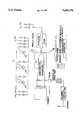
- the FIGUREis a schematic diagram of the LP-MOCVD reactor for use in the method of the subject invention.
- the reactor and associated gas-distribution scheme used herein shown in FIGUREThe system consists of a cooled quartz reaction tube (diameter 5 cm in the substrate area) pumped by a high-capacity roughing pump (120 hr -1 ) to a vacuum between 10 and 300 Torr.
- the substratewas mounted on a pyrolytically coated graphite susceptor that was heated by rf induction at 1 MHz.
- the pressure inside the reactorwas measured by a mechanical gauge and the temperature by an infrared pyrometer.
- a molecular sievewas used to impede oil back-diffusion at the input of the pump.
- the working pressurewas adjusted by varying the flow rate of the pump by using a control gate valve.
- the gas panelwas classical, using 1/4-inch stainless steel tubes and Swagelock fittings. Flow rates were controlled by mass flowmeters.
- the reactorwas purged with a nitrogen flow of 4 liters min -1 , and the working pressure of 75 Torr was established by opening the gate valve that separated the pump and the reactor.
- the evacuation line that was used at atmospheric pressurewas automatically closed by the opening of the gate valve.
- the gas flow rateswere measured under standard conditions, i.e., 1 atm and 20° C., even when the reactor was at subatmospheric pressure.
- the pressure in the gas panelwas regulated by the needle valve placed between the gas panel and the reactor. The needle valve was adjusted to maintain a constant pressure of 1 atm on the gas panel, thereby ensuring reproducibility of flow-rate measurements.
- group-III speciesi.e., trimethyl, indium (TMI), triethyl indium (TEI), and cyclopentadienyl thallium (CpTl), are contained in stainless steel bubblers, which are held in controlled temperature baths at 31° and 0° C., respectively.
- An accurately metered flow of purified H 2 for TMI and CpTlis passed through the appropriate bubbler.
- the saturated vapor that emerges from the bottleis immediately diluted by a flow of hydrogen.
- Nitrogenmay also be used as a carrier gas.
- the mole fraction, and thus the partial pressure, of the source speciesis lower in the mixture and is prevented from condensing in the stainless steel pipe work.
- ethyl phosphorousEt 3 P
- Me 3 Pmethyl phosphorous
- t-BuPt-butyl phosphorous
- PH 3phosphine
- the metal alkyl or hydride flowcan be either injected into the reactor or into the waste line by using three-way valves. In each case, the source flow is first switched into the waste line to establish the flow rate and then switched into the reactor.
- the total gas flow rateis 8 liters min -1 . Stable flows are achieved by the use of mass flow controllers.
- Semi-insulating or n + substratesare supplied by MCP, Crystacomm, Metals Research, or Sumitomo in the form of ingots or polished wafers. Wafers are sliced 2° off (100) toward (110) and chemically etched for 10 seconds at room temperature in a 15% bromine-methanol solution in order to remove 20 ⁇ m from each side. The wafers were then mechanochemically polished in a solution of 1.5% bromine in methanol, removing a further 80-100 ⁇ m. The substrates were finally cleaned in methanol and rinsed in isopropyl alcohol.
- the substrateswere etched again, just before use, by dipping in 1% bromine in methanol at room temperature for one minute, rinsing in warm isopropyl alcohol, and drying.
- An n + tin-doped substrate and a semi-insulating iron-doped substratewere generally used for each experiment.
- the epitaxial layer qualityis sensitive to the pretreatment of the substrate and the alloy composition.
- Pretreatment of the substrates prior to epitaxial growthwas thus found to be beneficial.
- One such pretreatment procedureis as follows:
- the hot susceptorhas a catalytic effect on the decomposition of the gaseous products; the growth rate is proportional to the flow rate of the group-III species but is independent of temperature between 470° and 540° C. and of the partial pressure of group-V species as well.
- the gas moleculesdiffuse across the boundary layer to the substrate surface, where the metal alkyls and hydrides decompose to produce the group-III and group-V elemental species.
- the elemental speciesmove on the hot surface until they find an available lattice site, where growth then occurs.
- High quality (InP) 1-x (TlP 3 ) xmay be grown in the method of the subject invention by low pressure metalorganic chemical vapor deposition (LP-MOCVD).
- LP-MOCVDlow pressure metalorganic chemical vapor deposition
- Other forms of deposition of III-V filmsmay be used as well, including MBE. (Molecular Beam Epitoxy), MOMBE (metalorganic molecular bean epitay), LPE (liquid phase epitaxy) and VPE (vapor phase epitaxy).
- the layers of the heterostructureare grown by the induction-heated horizontal cool wall reactor of FIG. 1, as described below in more detail.
- Trimethylindium (TMI) and cyclopentadienyl thallium (CpTl)are used as the sources of indium and thallium respectively.
- Pure phosphine (PH 3 ) supplied by Matheson Inc.is used as the P source.
- Sampleis grown on a Fe doped InP substrate. The optimum growth conditions are listed in the Table, Doping of the substrate is conducted with elemental Fe for p-type doping and SiH 4 for n-type doping.
- Doping of the epilayercan be conducted with n-type dopants such as H 2 S OR SiH 4 , or with p-type dopants such as diethylzinc. Doping is performed through the bubbler shown in FIG. 1 with H 2 as carrier gas and at temperatures from -15° C. to ambient temperatures at 20-90 cm 3 min. -1 and onto either a hot or cooled substrate (535° C.). SiH 4 may be simply directed at ambient temperatures onto the hot substrate at 20-90 cm 3 min..sup. -1.
- the heat sourceis terminated and the substrate allowed to cool; the metal and hydride sources are terminated; the dopant flow, for instance, is initiated at the temperatures indicated for diffusion onto the cooled substrate/epilayer which has been previously grown. After about 2-3 minutes, the dopant flow is terminated and the next epilayer grown.
- the InP layercan be grown at approximately 70-80 Torr and preferably 76 Torr and low temperature, between 470° and 540° C., preferably 510° C., by using TMI and PH 3 in H 2 or N 2 , or H 2 and N 2 carrier gas.
- Thalliumcan be introduced at 76 Torr and low temperature, between 470° and 540° C. and preferably 510° C., using CpTl in a H 2 or N 2 or H 2 and N 2 carrier gas.
- Uniform composition (InP) x-1 (TlP 3 ) x over an area of 10 cm 2 of InP substratehas been obtained.
- the growth rateis small (5 ⁇ sec -1 ), and it takes less than 1 second for the gas flow to reach its new steady state.
- Epilayers of 10 ⁇ to 5 ⁇ m thickcan be grown by the method of the subject invention, dependent on whether a photodetector use or a laser use is required.
- the thickness of an epilayerwas measured by a bevel stain technique (solution),and the composition calculated either from the PL wavelength or from the value of the lattice parameter as measured by single-crystal x-ray diffraction.
- the epilayer of (InP) x-1 (TlP 3 ) xare grown as follows.
- a semiconductor alloy for an infrared detectorwas prepared on an InP substrate according to the above methods and in the following manner. First, a 400- ⁇ m thick InP substrate doped with Fe and/or Sn is prepared and cleaned. A 01.5 ⁇ m epilayer of InP, is grown on the Fe and Sn doped InP substrates. The growth temperature was 510° C. for 90 minutes. A flow of CpTl was introduced at 510° C. for 30 minutes. The resulting (InP) x-1 (TlP 3 ) x epilayer was 1.05 ⁇ m thick.
Landscapes
- Physics & Mathematics (AREA)
- Condensed Matter Physics & Semiconductors (AREA)
- General Physics & Mathematics (AREA)
- Electromagnetism (AREA)
- Optics & Photonics (AREA)
- Chemical Vapour Deposition (AREA)
Abstract
Description
This application relates to semiconductor III-V alloy compounds, and more particularly to a method of making III-V alloy compounds for use in photonic and electronic devices such as diode lasers and photodetectors.
The growth of semiconductor III-V compounds by chemical vapor deposition (CVD) using organometallics and hydrides as elemental sources has recently developed into a viable process with many potential commercial applications. The metallo-organic chemical vapor deposition (MOCVD) process, based on the pyrolysis of alkyls of group-III elements in an atmosphere of the hydrides of group-V elements, is a common growth technique because it is well adapted to the growth of submicron layers and heterostructures.
Open-tube flow systems are used at atmospheric or reduced pressures in producing the III-V alloys. The process requires only one high-temperature zone for the in situ formation and growth of the semiconductor compound directly on a heated substrate.
Low pressure (LP-) MOCVD growth method offers an improved thickness uniformity and compositional homogeneity, reduction of autodoping, reduction of parasitic decomposition in the gas phase, and allows the growth of high-quality material over a large surface area. Growth by MOCVD takes place far from a thermodynamic equilibrium, and growth rates are determined generally by the arrival rate of material at the growing surface rather than by temperature-dependent reactions between the gas and solid phases.
There have been many III-V materials investigated for long wavelength (8-12 μm) infrared detector applications. So far, InAsSb is the III-V semiconductor alloy with the smallest energy bandgap, but its bandgap is not large enough to cover the entire 8-12 μm range. Even though further reduction in the bandgap has been achieved using strained-layer InAsSb/InSb superlattices, no lattice-matched substrate is available for these materials, so that there remains the problem of obtaining device-quality materials. InTlSb has successfully grown by low-pressure metalorganic chemical vapor deposition (LP-MOCVD) and a reduction in the bandgap energy of 100 MeV was confirmed through optical characterizations. The lattice of InTlSb was found to contact with increased thallium content and the resulting mismatch with InSb was found to be larger than the predicted estimate. Moreover, a solubility limit of thallium in InSb has been calculated to be ˜15%, beyond which a two-phase region consisting of zinc-blend and CsCl-type structures is predicted. As a result, it is concluded that InTlSb/InSb is inoperative for use in semiconductor applications.
An object, therefore, of the invention is the growth of high quality III-V materials with a bandgap in the 2-12 μm range.
A further object of the subject invention is a InTlP grown by low-pressure metalorganic chemical vapor deposition (LP-MOCVD).
A still further object of the subject invention an alloy of the composition (InP)1-x (TlP3)x for use as an infrared material for use in lasers and photodetectors, where x is between 0.1 and 0.9.
These and other objects are attained by the subject invention comprising (InP)1-x (TlP3)x which is prepared by growing an InP epilayer on a semi-insulating p(Fe) doped or n+ (Sn) doped InP substrate through LP-MOCVD. In the method of the subject invention, trimethylindium and phosphine were used as the sources of In and P. The growth temperature and pressure was maintained at 510° C. and 76 torr, respectively. Growth of (InP)1-x (TlP3)x (0.1≦x≦0.9) was performed on the InP substrate by introducing a small flow of cyclopentadienylthallium (CpTl) without perturbing other growth conditions. The (InP)x-1 (TlP)x layer may be doped to vary the properties of the epilayer.
The FIGURE is a schematic diagram of the LP-MOCVD reactor for use in the method of the subject invention.
The reactor and associated gas-distribution scheme used herein shown in FIGURE. The system consists of a cooled quartz reaction tube (diameter 5 cm in the substrate area) pumped by a high-capacity roughing pump (120 hr-1) to a vacuum between 10 and 300 Torr. The substrate was mounted on a pyrolytically coated graphite susceptor that was heated by rf induction at 1 MHz. The pressure inside the reactor was measured by a mechanical gauge and the temperature by an infrared pyrometer. A molecular sieve was used to impede oil back-diffusion at the input of the pump. The working pressure was adjusted by varying the flow rate of the pump by using a control gate valve. The gas panel was classical, using 1/4-inch stainless steel tubes and Swagelock fittings. Flow rates were controlled by mass flowmeters.
The reactor was purged with a nitrogen flow of 4 liters min-1, and the working pressure of 75 Torr was established by opening the gate valve that separated the pump and the reactor. The evacuation line that was used at atmospheric pressure was automatically closed by the opening of the gate valve. The gas flow rates were measured under standard conditions, i.e., 1 atm and 20° C., even when the reactor was at subatmospheric pressure. The pressure in the gas panel was regulated by the needle valve placed between the gas panel and the reactor. The needle valve was adjusted to maintain a constant pressure of 1 atm on the gas panel, thereby ensuring reproducibility of flow-rate measurements.
The gas source used in this study for the growth of InP and (InP)1-x (TlP3)x by LP-MOCVD are listed in the accompanying tabulation. The organometallic
______________________________________ Group-III Sources Group-V Sources ______________________________________ In (C.sub.2 H.sub.5).sub.3 Et.sub.3 P In (CH.sub.3).sub.3 Me.sub.3 P CpTl t-BuP PH.sub.3 ______________________________________
group-III species i.e., trimethyl, indium (TMI), triethyl indium (TEI), and cyclopentadienyl thallium (CpTl), are contained in stainless steel bubblers, which are held in controlled temperature baths at 31° and 0° C., respectively. An accurately metered flow of purified H2 for TMI and CpTl is passed through the appropriate bubbler. To ensure that the source material remains in vapor form, the saturated vapor that emerges from the bottle is immediately diluted by a flow of hydrogen. Nitrogen may also be used as a carrier gas. The mole fraction, and thus the partial pressure, of the source species is lower in the mixture and is prevented from condensing in the stainless steel pipe work.
Pure ethyl phosphorous (Et3 P), methyl phosphorous (Me3 P), t-butyl phosphorous (t-BuP) or phosphine (PH3) are used as sources of P. The metal alkyl or hydride flow can be either injected into the reactor or into the waste line by using three-way valves. In each case, the source flow is first switched into the waste line to establish the flow rate and then switched into the reactor. The total gas flow rate is 8 liters min-1. Stable flows are achieved by the use of mass flow controllers.
Semi-insulating or n+ substrates are supplied by MCP, Crystacomm, Metals Research, or Sumitomo in the form of ingots or polished wafers. Wafers are sliced 2° off (100) toward (110) and chemically etched for 10 seconds at room temperature in a 15% bromine-methanol solution in order to remove 20 μm from each side. The wafers were then mechanochemically polished in a solution of 1.5% bromine in methanol, removing a further 80-100 μm. The substrates were finally cleaned in methanol and rinsed in isopropyl alcohol. The substrates were etched again, just before use, by dipping in 1% bromine in methanol at room temperature for one minute, rinsing in warm isopropyl alcohol, and drying. An n+ tin-doped substrate and a semi-insulating iron-doped substrate were generally used for each experiment.
The epitaxial layer quality is sensitive to the pretreatment of the substrate and the alloy composition.
Pretreatment of the substrates prior to epitaxial growth was thus found to be beneficial. One such pretreatment procedure is as follows:
1. Dipping in H2 SO4 for 3 minutes with ultrasonic agitation;
2. Rinsing in Deionized H2 O;
3. Rinsing in hot methanol;
4. Dipping in 3% Br in methanol at room temperature for 3 minutes (ultrasonic bath);
5. Rinsing in hot methanol;
6. Dipping in H2 SO4 for 3 minutes;
7. Rinsing in deionized H2 O, and
8. Rinsing in hot methanol.
After this treatment, it is possible to preserve the substrate for one or two weeks without repeating this treatment prior to growth.
Growth takes place by introducing metered amounts of the group-III alkyls and the group-V hydrides into a quartz reaction tube containing a substrate placed on an rf-heated susceptor surface. The hot susceptor has a catalytic effect on the decomposition of the gaseous products; the growth rate is proportional to the flow rate of the group-III species but is independent of temperature between 470° and 540° C. and of the partial pressure of group-V species as well. The gas molecules diffuse across the boundary layer to the substrate surface, where the metal alkyls and hydrides decompose to produce the group-III and group-V elemental species. The elemental species move on the hot surface until they find an available lattice site, where growth then occurs.
High quality (InP)1-x (TlP3)x may be grown in the method of the subject invention by low pressure metalorganic chemical vapor deposition (LP-MOCVD). Other forms of deposition of III-V films may be used as well, including MBE. (Molecular Beam Epitoxy), MOMBE (metalorganic molecular bean epitay), LPE (liquid phase epitaxy) and VPE (vapor phase epitaxy).
In the MOCVD method the layers of the heterostructure are grown by the induction-heated horizontal cool wall reactor of FIG. 1, as described below in more detail. Trimethylindium (TMI) and cyclopentadienyl thallium (CpTl) are used as the sources of indium and thallium respectively. Pure phosphine (PH3) supplied by Matheson Inc. is used as the P source. Sample is grown on a Fe doped InP substrate. The optimum growth conditions are listed in the Table, Doping of the substrate is conducted with elemental Fe for p-type doping and SiH4 for n-type doping. Doping of the epilayer can be conducted with n-type dopants such as H2 S OR SiH4, or with p-type dopants such as diethylzinc. Doping is performed through the bubbler shown in FIG. 1 with H2 as carrier gas and at temperatures from -15° C. to ambient temperatures at 20-90 cm3 min.-1 and onto either a hot or cooled substrate (535° C.). SiH4 may be simply directed at ambient temperatures onto the hot substrate at 20-90 cm3 min..sup. -1.
In a preferred doping method for incorporating the maximum amount of dopant on a layer, once the layer to be doped is fully grown, the heat source is terminated and the substrate allowed to cool; the metal and hydride sources are terminated; the dopant flow, for instance, is initiated at the temperatures indicated for diffusion onto the cooled substrate/epilayer which has been previously grown. After about 2-3 minutes, the dopant flow is terminated and the next epilayer grown.
TABLE 1 ______________________________________ Optimum growth conditions of (InP).sub.1-x (T1P.sub.3).sub.x structure on a InP substrate. ______________________________________ Growth Pressure 76 (Torr) Growth Temperature 510 (°C.) Total H.sub.2 Flow 3 (liter/min) TMI (cc/min) 120 PH.sub.3 (cc/min 30 CpTl 10 Growth Rate 150 (Å/min) ______________________________________
The InP layer can be grown at approximately 70-80 Torr and preferably 76 Torr and low temperature, between 470° and 540° C., preferably 510° C., by using TMI and PH3 in H2 or N2, or H2 and N2 carrier gas.
Thallium can be introduced at 76 Torr and low temperature, between 470° and 540° C. and preferably 510° C., using CpTl in a H2 or N2 or H2 and N2 carrier gas. Uniform composition (InP)x-1 (TlP3)x over an area of 10 cm2 of InP substrate has been obtained. The growth rate is small (5 Å sec-1), and it takes less than 1 second for the gas flow to reach its new steady state. Epilayers of 10 Å to 5 μm thick can be grown by the method of the subject invention, dependent on whether a photodetector use or a laser use is required.
The thickness of an epilayer was measured by a bevel stain technique (solution),and the composition calculated either from the PL wavelength or from the value of the lattice parameter as measured by single-crystal x-ray diffraction. The epilayer of (InP)x-1 (TlP3)x are grown as follows.
A semiconductor alloy for an infrared detector was prepared on an InP substrate according to the above methods and in the following manner. First, a 400-μm thick InP substrate doped with Fe and/or Sn is prepared and cleaned. A 01.5 μm epilayer of InP, is grown on the Fe and Sn doped InP substrates. The growth temperature was 510° C. for 90 minutes. A flow of CpTl was introduced at 510° C. for 30 minutes. The resulting (InP)x-1 (TlP3)x epilayer was 1.05 μm thick.
The structural, electrical, and optical properties of these films were then compared using X-ray diffraction system, electrochemical C-V (ECV) profiler, Hall system, and photolumincscence (PL). X-ray diffraction measurements of both samples showed one sharp peak at an angle corresponding to InP. This is not an unexpected result for the (InP)1-x (TlP3)x film since the lattice-mismatch should be negligible for such thallium concentrations. A large difference between the two films was observed in their electrical characteristics. In comparison to the hall mobility of InP (20,000 cm2 /Vs) measured at 77K, the mobility of the (InP)1-x (TlP3) sample was nearly an order lower (3000 cm2 /Vs). At the same time, the carrier concentration determined by both Hall measurements and ECV profiler was higher for the (InP)1-x (TlP3)x sample. ECV profile also revealed a difference in the thickness of the two epilayers which were both grown for 3 hours. From this measurement, the respective growth rates of InP and (InP)1-x (TlP3)x were calculated to be approximately 0.50 μ m/hr and 0.65 μm/hr.
In optical measurements, a PL experiment performed on InP/InP at 77K displayed a lone peak around 880 nm which corresponds to the luminescence wavelength of InP. For (InP)1-x (TlP3)x /InP, a peak at a wavelength around 7 μm was observed in addition to an InP peak at 880 nm. In order to confirm this observation, photoconductivity measurement was carried out on the (InP)1-x (TlP3)x /InP sample at 77K. For this experiment, the clover-shaped sample patterned for the Hall measurement was used. The measurement showed a weak but a definite photoresponse with a cut-off wavelength around 6-7 μm.
From the above it is concluded that a (InP)1-x (TlP3)x film (0.1≦x≦0.9) has a stable zinc blende structure with a maximum lattice mismatch between the endpoints of 1.28%. Further the film of the subject invention accepts both p-doping and n-doping. A bandgap of about 7 μm is observed, thereby making it suitable for long wavelength infrared detector applications as well as lasers.
While the invention has been described with reference to a preferred embodiment, it will be understood by those skilled in the art that various changes may be made and equivalents may be substituted for elements thereof without departing from the scope of the invention. In addition, many modifications may be made to adapt a particular situation or material to the teachings of the invention without departing from the essential scope thereof. Therefore, it is intended that the invention not be limited to the particular embodiment disclosed as the best mode contemplated for carrying out this invention, but that the invention will include all embodiments and equivalents falling within the scope of the appended claims.
Various features of the invention are set forth in the following claims.
Claims (3)
1. An alloy for use as a semiconductor film comprising (InP)1-x (TlP3)x where 0.1≦x≦0.9.
2. The alloy of claim 1 wherein said alloy has a zinc blende structure.
3. The alloy of claim 1 wherein said alloy is doped with a p-type element or a n-type element.
Priority Applications (4)
| Application Number | Priority Date | Filing Date | Title |
|---|---|---|---|
| US08/293,903US5410178A (en) | 1994-08-22 | 1994-08-22 | Semiconductor films |
| US08/354,225US5462008A (en) | 1994-08-22 | 1994-12-12 | Semiconductor films |
| PCT/US1995/009983WO1996006461A1 (en) | 1994-08-22 | 1995-08-07 | Improved semiconductor films |
| AU32401/95AAU3240195A (en) | 1994-08-22 | 1995-08-07 | Improved semiconductor films |
Applications Claiming Priority (1)
| Application Number | Priority Date | Filing Date | Title |
|---|---|---|---|
| US08/293,903US5410178A (en) | 1994-08-22 | 1994-08-22 | Semiconductor films |
Related Child Applications (1)
| Application Number | Title | Priority Date | Filing Date |
|---|---|---|---|
| US08/354,225DivisionUS5462008A (en) | 1994-08-22 | 1994-12-12 | Semiconductor films |
Publications (1)
| Publication Number | Publication Date |
|---|---|
| US5410178Atrue US5410178A (en) | 1995-04-25 |
Family
ID=23131060
Family Applications (2)
| Application Number | Title | Priority Date | Filing Date |
|---|---|---|---|
| US08/293,903Expired - Fee RelatedUS5410178A (en) | 1994-08-22 | 1994-08-22 | Semiconductor films |
| US08/354,225Expired - Fee RelatedUS5462008A (en) | 1994-08-22 | 1994-12-12 | Semiconductor films |
Family Applications After (1)
| Application Number | Title | Priority Date | Filing Date |
|---|---|---|---|
| US08/354,225Expired - Fee RelatedUS5462008A (en) | 1994-08-22 | 1994-12-12 | Semiconductor films |
Country Status (3)
| Country | Link |
|---|---|
| US (2) | US5410178A (en) |
| AU (1) | AU3240195A (en) |
| WO (1) | WO1996006461A1 (en) |
Cited By (8)
| Publication number | Priority date | Publication date | Assignee | Title |
|---|---|---|---|---|
| US5599732A (en)* | 1995-08-21 | 1997-02-04 | Northwestern University | Method for growing III-V semiconductor films using a coated reaction chamber |
| USRE36315E (en)* | 1994-08-12 | 1999-09-28 | S.R.I. International | Compounds and infrared devices including stoichiometric semiconductor compounds of indium, thallium, and including at least one of arsenic and phosphorus |
| US20050034661A1 (en)* | 1998-12-21 | 2005-02-17 | Finisar Corporation | System for developing a nitrogen-containing active region |
| US20050098380A1 (en)* | 2003-09-23 | 2005-05-12 | Luscombe Terry L. | Vehicle mounted utility apparatus with quick attachment means |
| JP2005244141A (en)* | 2004-02-27 | 2005-09-08 | Toyo Univ | InSb nanowire structure |
| US20070201525A1 (en)* | 2004-10-01 | 2007-08-30 | Finisar Corporation | Vertical cavity surface emitting laser having strain reduced quantum wells |
| US20110090930A1 (en)* | 2004-10-01 | 2011-04-21 | Finisar Corporation | Vertical cavity surface emitting laser with undoped top mirror |
| CN112730549A (en)* | 2021-01-13 | 2021-04-30 | 福建中科光芯光电科技有限公司 | Method for improving semiconductor doping concentration test precision |
Families Citing this family (4)
| Publication number | Priority date | Publication date | Assignee | Title |
|---|---|---|---|---|
| FR2775388B1 (en)* | 1998-02-26 | 2001-12-07 | Sagem | INDIUM-BASED ALLOY AND INFRARED TRANSDUCER USING SUCH ALLOY |
| JP2000058971A (en)* | 1998-08-04 | 2000-02-25 | Mitsubishi Electric Corp | Semiconductor laser device and method of manufacturing the same |
| DE10007059A1 (en)* | 2000-02-16 | 2001-08-23 | Aixtron Ag | Method and device for producing coated substrates by means of condensation coating |
| JP2022065415A (en)* | 2020-10-15 | 2022-04-27 | ウシオ電機株式会社 | Infrared LED element |
Citations (13)
| Publication number | Priority date | Publication date | Assignee | Title |
|---|---|---|---|---|
| US3364084A (en)* | 1959-06-18 | 1968-01-16 | Monsanto Co | Production of epitaxial films |
| US3663320A (en)* | 1968-08-02 | 1972-05-16 | Nippon Electric Co | Vapor growth process for gallium arsenide |
| US3849874A (en)* | 1972-07-28 | 1974-11-26 | Bell & Howell Co | Method for making a semiconductor strain transducer |
| US4207122A (en)* | 1978-01-11 | 1980-06-10 | International Standard Electric Corporation | Infra-red light emissive devices |
| US4368098A (en)* | 1969-10-01 | 1983-01-11 | Rockwell International Corporation | Epitaxial composite and method of making |
| US4404265A (en)* | 1969-10-01 | 1983-09-13 | Rockwell International Corporation | Epitaxial composite and method of making |
| US4720309A (en)* | 1985-07-23 | 1988-01-19 | Benoit Deveaud | Saturatable absorbant with very short switching times |
| US4793872A (en)* | 1986-03-07 | 1988-12-27 | Thomson-Csf | III-V Compound heteroepitaxial 3-D semiconductor structures utilizing superlattices |
| US4874438A (en)* | 1986-04-01 | 1989-10-17 | Toyo Communication Equipment Co., Ltd. | Intermetallic compound semiconductor thin film and method of manufacturing same |
| US4902356A (en)* | 1988-01-21 | 1990-02-20 | Mitsubishi Monsanto Chemical Company | Epitaxial substrate for high-intensity led, and method of manufacturing same |
| US4908686A (en)* | 1988-08-01 | 1990-03-13 | California Institute Of Technology | Stacked silicide/silicon mid- to long-wavelength infrared detector |
| US4952811A (en)* | 1989-06-21 | 1990-08-28 | The United States Of America As Represented By The Administrator Of The National Aeronautics And Space Administration | Field induced gap infrared detector |
| US5232869A (en)* | 1991-07-30 | 1993-08-03 | Shell Research Limited | Metal deposition |
Family Cites Families (7)
| Publication number | Priority date | Publication date | Assignee | Title |
|---|---|---|---|---|
| US3696262A (en)* | 1970-01-19 | 1972-10-03 | Varian Associates | Multilayered iii-v photocathode having a transition layer and a high quality active layer |
| US3805601A (en)* | 1972-07-28 | 1974-04-23 | Bell & Howell Co | High sensitivity semiconductor strain gauge |
| US4782034A (en)* | 1987-06-04 | 1988-11-01 | American Telephone And Telegraph Company, At&T Bell Laboratories | Semi-insulating group III-V based compositions doped using bis arene titanium sources |
| JPS63276895A (en)* | 1987-05-08 | 1988-11-15 | Hitachi Ltd | Manufacture for electroluminescent element |
| JPH0817160B2 (en)* | 1987-10-06 | 1996-02-21 | 昭和電工株式会社 | Vapor growth method |
| NL8802458A (en)* | 1988-10-07 | 1990-05-01 | Philips Nv | PROCESS FOR THE MANUFACTURE OF AN EPITAXIAL INDIUM PHOSPHIDE LAYER ON A SUBSTRATE SURFACE. |
| JPH0388324A (en)* | 1989-08-31 | 1991-04-12 | Nippon Telegr & Teleph Corp <Ntt> | Method for forming compound semiconductor thin film |
- 1994
- 1994-08-22USUS08/293,903patent/US5410178A/ennot_activeExpired - Fee Related
- 1994-12-12USUS08/354,225patent/US5462008A/ennot_activeExpired - Fee Related
- 1995
- 1995-08-07AUAU32401/95Apatent/AU3240195A/ennot_activeAbandoned
- 1995-08-07WOPCT/US1995/009983patent/WO1996006461A1/enactiveApplication Filing
Patent Citations (13)
| Publication number | Priority date | Publication date | Assignee | Title |
|---|---|---|---|---|
| US3364084A (en)* | 1959-06-18 | 1968-01-16 | Monsanto Co | Production of epitaxial films |
| US3663320A (en)* | 1968-08-02 | 1972-05-16 | Nippon Electric Co | Vapor growth process for gallium arsenide |
| US4368098A (en)* | 1969-10-01 | 1983-01-11 | Rockwell International Corporation | Epitaxial composite and method of making |
| US4404265A (en)* | 1969-10-01 | 1983-09-13 | Rockwell International Corporation | Epitaxial composite and method of making |
| US3849874A (en)* | 1972-07-28 | 1974-11-26 | Bell & Howell Co | Method for making a semiconductor strain transducer |
| US4207122A (en)* | 1978-01-11 | 1980-06-10 | International Standard Electric Corporation | Infra-red light emissive devices |
| US4720309A (en)* | 1985-07-23 | 1988-01-19 | Benoit Deveaud | Saturatable absorbant with very short switching times |
| US4793872A (en)* | 1986-03-07 | 1988-12-27 | Thomson-Csf | III-V Compound heteroepitaxial 3-D semiconductor structures utilizing superlattices |
| US4874438A (en)* | 1986-04-01 | 1989-10-17 | Toyo Communication Equipment Co., Ltd. | Intermetallic compound semiconductor thin film and method of manufacturing same |
| US4902356A (en)* | 1988-01-21 | 1990-02-20 | Mitsubishi Monsanto Chemical Company | Epitaxial substrate for high-intensity led, and method of manufacturing same |
| US4908686A (en)* | 1988-08-01 | 1990-03-13 | California Institute Of Technology | Stacked silicide/silicon mid- to long-wavelength infrared detector |
| US4952811A (en)* | 1989-06-21 | 1990-08-28 | The United States Of America As Represented By The Administrator Of The National Aeronautics And Space Administration | Field induced gap infrared detector |
| US5232869A (en)* | 1991-07-30 | 1993-08-03 | Shell Research Limited | Metal deposition |
Non-Patent Citations (56)
| Title |
|---|
| Accurate determination of misfit strain, layer thickness, and critical layer thickness in ultrathin buried strained InGaAs/GaAs layer b x ray diffraction, Y. C. Chen, P. K. Bhattacharya and J. Singh, American Vacuum Society, Mar./Apr. 1992, pp. 769 770.* |
| Accurate determination of misfit strain, layer thickness, and critical layer thickness in ultrathin buried strained InGaAs/GaAs layer b x-ray diffraction, Y. C. Chen, P. K. Bhattacharya and J. Singh, American Vacuum Society, Mar./Apr. 1992, pp. 769-770. |
| Applied Physics Letters, Photoconductance measurements on InTlSb/InSb/GaAs grown by low pressure metalorganic chemical vapor deposition, P. T. Staveteig, Y. H. Choi, G. Labeyrie, E. Bigan and M. Razeghi, American Institute of Physics, 24 Jan. 1994, vol. 64, No. 4, pp. 460 462.* |
| Applied Physics Letters, Photoconductance measurements on InTlSb/InSb/GaAs grown by low-pressure metalorganic chemical vapor deposition, P. T. Staveteig, Y. H. Choi, G. Labeyrie, E. Bigan and M. Razeghi, American Institute of Physics, 24 Jan. 1994, vol. 64, No. 4, pp. 460-462. |
| Chapter 1 Growth Technolgy, C. Hilsum, Aug. 1988.* |
| Chapter 4 GaInAsP InP Systems: MOCVD Growth, Characterization and Application, pp. 164 215.* |
| Chapter 4 GaInAsP-InP Systems: MOCVD Growth, Characterization and Application, pp. 164-215. |
| Chapter 5: Low Pressure Metallo Organic Chemical Vapor Deposition of Ga x In 1 x As y P 1 y Alloys, Manijeh Razeghi, Semiconductors and Semimetals, vol. 22, Part A pp. 300 378.* |
| Chapter 5: Low-Pressure Metallo-Organic Chemical Vapor Deposition of Gax In1-x Asy P1-y Alloys, Manijeh Razeghi, Semiconductors and Semimetals, vol. 22, Part A pp. 300-378. |
| Dictionary of Physics, Longmans, Greens and Co. Ltd., p. 292.* |
| Efficiency of photoluminescence and excess carrier confinement in InGaAsP/GaAs structures prepared by metalorganic chemical vapor deposition, J. Diaz, J. Yi, M. Erdtmann, X. He, E. Kolev, D. Garbuzov, E. Bigan and M. Raseghi, American Institute of Physics, 15 Jul. 1994, pp. 700 704.* |
| Efficiency of photoluminescence and excess carrier confinement in InGaAsP/GaAs structures prepared by metalorganic chemical-vapor deposition, J. Diaz, J. Yi, M. Erdtmann, X. He, E. Kolev, D. Garbuzov, E. Bigan and M. Raseghi, American Institute of Physics, 15 Jul. 1994, pp. 700-704. |
| Electron Transport Properties of Ga 0.51 In 0.49 P for Device Applications, C. Besikci and M. Razeghi, IEEE, 1994, pp. 1066 1069.* |
| Electron Transport Properties of Ga0.51 In0.49 P for Device Applications, C. Besikci and M. Razeghi, IEEE, 1994, pp. 1066-1069. |
| Ga 0.51 In 0.49 P/Ga x In 1 x As lattice matched (x 1) and strained (x 0.85) two dimensional electron gas field effect transistors, M. Razeghi, F. Omnes, Ph Maurel, Y. J. Chan and D. Pavlidis, IOP Publishing Ltd, 1991, pp. 103 107.* |
| Ga0.51 In0.49 P/Gax In1-x As lattice-matched (x=1) and strained (x=0.85) two-dimensional electron gas field-effect transistors, M. Razeghi, F. Omnes, Ph Maurel, Y. J. Chan and D. Pavlidis, IOP Publishing Ltd, 1991, pp. 103-107. |
| Gas source molecular beam epitaxial growth of normal incidence GaAs/AlGaAs quantum well infrared photodectors, J. M. Kuo, S. S. Pei, S. Hui, S. D. Gunapala and B. F. Levine, American Vacuum Society, Mar./Apr. 1992, pp. 769 770.* |
| Gas source molecular-beam epitaxial growth of normal incidence GaAs/AlGaAs quantum well infrared photodectors, J. M. Kuo, S. S. Pei, S. Hui, S. D. Gunapala and B. F. Levine, American Vacuum Society, Mar./Apr. 1992, pp. 769-770. |
| Growth of In 1 x Tl x Sb, a new infrared material, by low pressure metalorganic chemical vapor deposition, Y. H. Choi, C. Besikci, R. Sudharsanan and M. Razeghi, American Institute of Physics, 19 Jun. 1993, pp. 361 363.* |
| Growth of In1-x Tlx Sb, a new infrared material, by low-pressure metalorganic chemical vapor deposition, Y. H. Choi, C. Besikci, R. Sudharsanan and M. Razeghi, American Institute of Physics, 19 Jun. 1993, pp. 361-363. |
| Growth of InSb and GaAs by metalorganic chemical vapor deposition, R. M. Biefeld, and G. A. Hebner, Elsevier Science Publishers B.V. ( North Holland ), 1991, pp. 272 278.* |
| Growth of InSb and GaAs by metalorganic chemical vapor deposition, R. M. Biefeld, and G. A. Hebner, Elsevier Science Publishers B.V. (North Holland), 1991, pp. 272-278. |
| Hawley s Condensed Chemical Dictionary (Twelfth Edition), Van Nostrand Reinhold, 1993, p. 38.* |
| Hawley's Condensed Chemical Dictionary (Twelfth Edition), Van Nostrand Reinhold, 1993, p. 38. |
| High mobility InSb grown by organometallic vapor phase epitaxy, D. K. Gaskill, G. T. Stauf and N. Bottka, American Institute of Physics, 29 Apr. 1991, pp. 1905 1907.* |
| High photoconductive gain in lateral InAsSb strained layer superlattice infrared detectors, S. R. Kurtz, R. M. Biefeld, L. R. Dawson, I. J. Fritz and T. E. Zipperian, American Institute of Physics, 14 Nov. 1988, pp. 1961 1963.* |
| High photoconductive gain in lateral InAsSb strained-layer superlattice infrared detectors, S. R. Kurtz, R. M. Biefeld, L. R. Dawson, I. J. Fritz and T. E. Zipperian, American Institute of Physics, 14 Nov. 1988, pp. 1961-1963. |
| High Power 0.8 m InGaAsP GaAs SCH SQW Lasers, D. Z. Garbuzov, N. Yu Antonishkis, A. D. Bondarev, A. B. Gulakov, S. N. Zhigulin, N. I. Katsavets, A. V. Kochergin and E. V. Rafailov (Invited Paper) IEEE, 1991, pp. 1531 1535.* |
| High power laser diodes based on InGaAsP alloys, M. Razeghi, Nature, vol. 369, 23 Jun. 1994, pp. 631 633.* |
| High-mobility InSb grown by organometallic vapor phase epitaxy, D. K. Gaskill, G. T. Stauf and N. Bottka, American Institute of Physics, 29 Apr. 1991, pp. 1905-1907. |
| High-Power 0.8 μm InGaAsP-GaAs SCH SQW Lasers, D. Z. Garbuzov, N. Yu Antonishkis, A. D. Bondarev, A. B. Gulakov, S. N. Zhigulin, N. I. Katsavets, A. V. Kochergin and E. V. Rafailov (Invited Paper) IEEE, 1991, pp. 1531-1535. |
| High-power laser diodes based on InGaAsP alloys, M. Razeghi, Nature, vol. 369, 23 Jun. 1994, pp. 631-633. |
| InGaP/InGaAsP/GaAs 0.808 m Separate Confinement Laser Diodes Grown by Metalorganic Chemical Vapor Deposition, J. Diaz, I. Eliashevich, K. Mobarhan, E. Kolev, L. J. Wang, D. Z. Garbuzov and M. Razeghi, IEEE, 1994, pp. 132 134.* |
| InGaP/InGaAsP/GaAs 0.808 μm Separate Confinement Laser Diodes Grown by Metalorganic Chemical Vapor Deposition, J. Diaz, I. Eliashevich, K. Mobarhan, E. Kolev, L. J. Wang, D. Z. Garbuzov and M. Razeghi, IEEE, 1994, pp. 132-134. |
| Interface roughness scattering in thin, undoped GaInP/GaAs quantum wells, W. C. Mitchel, G. J. Brown and Ikai Lo, American Institute of Physics, 19 Sep. 1994, pp. 1578 1580.* |
| Interface roughness scattering in thin, undoped GaInP/GaAs quantum wells, W. C. Mitchel, G. J. Brown and Ikai Lo, American Institute of Physics, 19 Sep. 1994, pp. 1578-1580. |
| InTlSb: An infrared detector material M. van Schilfgaarde and A. Sher, American Institute of Physics, 19 Apr. 1993, pp. 1857 1859.* |
| InTlSb: An infrared detector material? M. van Schilfgaarde and A. Sher, American Institute of Physics, 19 Apr. 1993, pp. 1857-1859. |
| Journal of Applied Physics, Y. H. Choi, P. T. Staveteig, E. Bigan and M. Razeghi, American Institute of Physics, vol. 75, No. 6, 15 Mar. 1994, pp. 3196 3198.* |
| Journal of Applied Physics, Y. H. Choi, P. T. Staveteig, E. Bigan and M. Razeghi, American Institute of Physics, vol. 75, No. 6, 15 Mar. 1994, pp. 3196-3198. |
| On the Description of the Collision Terms in Three Valley Hydrodynamic Models for GaAs Device Modeling, C. Besikci and M. Razeghi, IEEE, vol. 41, No. 8, Aug. 1994, pp. 1471 1475.* |
| On the Description of the Collision Terms in Three-Valley Hydrodynamic Models for GaAs Device Modeling, C. Besikci and M. Razeghi, IEEE, vol. 41, No. 8, Aug. 1994, pp. 1471-1475. |
| Organometallic vapor phase epitaxial growth and characterization of InAsBi and InAsBi and InAsSbBi, K. Y. Ma, Z. M. Fang, D. H. Jaw, R. M. Cohen and G. B. Stringfellow, American Institute of Physics, 4 Dec. 1989, pp. 2420 2422.* |
| Organometallic vapor phase epitaxial growth and characterization of InAsBi and InAsBi and InAsSbBi, K. Y. Ma, Z. M. Fang, D. H. Jaw, R. M. Cohen and G. B. Stringfellow, American Institute of Physics, 4 Dec. 1989, pp. 2420-2422. |
| P Tl (Phosphorus Thallium), R. C. Sharma and Y. A. Chang, Binary Alloy Phase Diagrams.* |
| Photoexcited escape probability, optical gain, and noise in quantum well infrared photodetectors, B. F. Levine, A. Zussman, S. D. Gunapala, M. T. Asom, J. M. Kuo and W. S. Hobson, American Institute of Physics, 1 Nov. 1992 pp. 4429 4443.* |
| Photoexcited escape probability, optical gain, and noise in quantum well infrared photodetectors, B. F. Levine, A. Zussman, S. D. Gunapala, M. T. Asom, J. M. Kuo and W. S. Hobson, American Institute of Physics, 1 Nov. 1992 pp. 4429-4443. |
| P-Tl (Phosphorus-Thallium), R. C. Sharma and Y. A. Chang, Binary Alloy Phase Diagrams. |
| Thallium incorporation in molecular beam epitaxial InSb, C. E. C. Wood, A. Noreika and M. Francombe, American Institute of Physics, May 15, 1986, pp. 3610 3612.* |
| Thallium incorporation in molecular-beam-epitaxial InSb, C. E. C. Wood, A. Noreika and M. Francombe, American Institute of Physics, May 15, 1986, pp. 3610-3612. |
| The Electrochemical Society, Inc., 184th Meeting Program, Oct. 10 15, 1993.* |
| The Electrochemical Society, Inc., 184th Meeting Program, Oct. 10-15, 1993. |
| The MOCVD Challenge vol. 1: A Survey of GaInAsP InP for Photonic and Electronic Applications, M. Razeghi, IOP Publishing Ltd, 1989, pp. 3 28.* |
| The MOCVD Challenge vol. 1: A Survey of GaInAsP-InP for Photonic and Electronic Applications, M. Razeghi, IOP Publishing Ltd, 1989, pp. 3-28. |
| Vapor Phase Epitaxial Growth and Characterization of Ga 1 y In 1 As 1 x P x , K. Sugiyama, H. Kojima, G. Enda and M. Shibata, Japanese Journal of Applied Physics, vol. 16, No. 12, Dec. 1977, pp. 2197 2203.* |
| Vapor Phase Epitaxial Growth and Characterization of Ga1-y In1 As1-x Px, K. Sugiyama, H. Kojima, G. Enda and M. Shibata, Japanese Journal of Applied Physics, vol. 16, No. 12, Dec. 1977, pp. 2197-2203. |
Cited By (10)
| Publication number | Priority date | Publication date | Assignee | Title |
|---|---|---|---|---|
| USRE36315E (en)* | 1994-08-12 | 1999-09-28 | S.R.I. International | Compounds and infrared devices including stoichiometric semiconductor compounds of indium, thallium, and including at least one of arsenic and phosphorus |
| US5599732A (en)* | 1995-08-21 | 1997-02-04 | Northwestern University | Method for growing III-V semiconductor films using a coated reaction chamber |
| US20050034661A1 (en)* | 1998-12-21 | 2005-02-17 | Finisar Corporation | System for developing a nitrogen-containing active region |
| US20050098380A1 (en)* | 2003-09-23 | 2005-05-12 | Luscombe Terry L. | Vehicle mounted utility apparatus with quick attachment means |
| JP2005244141A (en)* | 2004-02-27 | 2005-09-08 | Toyo Univ | InSb nanowire structure |
| US20070201525A1 (en)* | 2004-10-01 | 2007-08-30 | Finisar Corporation | Vertical cavity surface emitting laser having strain reduced quantum wells |
| US20110090930A1 (en)* | 2004-10-01 | 2011-04-21 | Finisar Corporation | Vertical cavity surface emitting laser with undoped top mirror |
| US8168456B2 (en) | 2004-10-01 | 2012-05-01 | Finisar Corporation | Vertical cavity surface emitting laser with undoped top mirror |
| US8451875B2 (en) | 2004-10-01 | 2013-05-28 | Finisar Corporation | Vertical cavity surface emitting laser having strain reduced quantum wells |
| CN112730549A (en)* | 2021-01-13 | 2021-04-30 | 福建中科光芯光电科技有限公司 | Method for improving semiconductor doping concentration test precision |
Also Published As
| Publication number | Publication date |
|---|---|
| US5462008A (en) | 1995-10-31 |
| AU3240195A (en) | 1996-03-14 |
| WO1996006461A1 (en) | 1996-02-29 |
Similar Documents
| Publication | Publication Date | Title |
|---|---|---|
| EP0586321B1 (en) | Formation of supersaturated rare earth doped semiconductor layers by CVD | |
| US6066204A (en) | High pressure MOCVD reactor system | |
| US4659401A (en) | Growth of epitaxial films by plasma enchanced chemical vapor deposition (PE-CVD) | |
| Duchemin et al. | GaInAs and GaInAsP materials grown by low pressure MOCVD for microwave and optoelectronic applications | |
| US5410178A (en) | Semiconductor films | |
| US4636268A (en) | Chemical beam deposition method utilizing alkyl compounds in a carrier gas | |
| Haywood et al. | Growth of GaSb by MOVPE; Optimization of electrical quality with respect to growth rate, pressure, temperature and IIIV ratio | |
| Kuech et al. | Disilane: A new silicon doping source in metalorganic chemical vapor deposition of GaAs | |
| US6271104B1 (en) | Fabrication of defect free III-nitride materials | |
| US6108360A (en) | Long wavelength DH, SCH and MQW lasers based on Sb | |
| US5389396A (en) | InGaAsP/GaAs diode laser | |
| US5663976A (en) | Buried-ridge laser device | |
| US5658825A (en) | Method of making an InAsSb/InAsSbP diode lasers | |
| Kurtz et al. | Incorporation of nitrogen into GaAsN grown by MOCVD using different precursors | |
| Oshima et al. | Evaluation of GaAs solar cells grown under different conditions via hydride vapor phase epitaxy | |
| US5384151A (en) | InGaAsP/GaAs diode laser | |
| US5821155A (en) | Method of growing n-type III-V semiconductor materials on a substrate using SiI4 | |
| US6461884B1 (en) | Diode laser | |
| Chen et al. | The use of triisopropylantimony for the growth of InSb and GaSb | |
| Ludowise et al. | Use of column V alkyls in organometallic vapor phase epitaxy (OMVPE) | |
| US7329554B2 (en) | Reactive codoping of GaAlInP compound semiconductors | |
| Tsang | Chemical beam epitaxy of InGaAs | |
| Thompson | The effects of substrate misorientation on silicon doping efficiency in MOVPE grown GaAs | |
| EP0138965A1 (en) | Tetramethyltin dopant source for mocvd grown epitaxial semiconductor layers. | |
| Noda et al. | ZnxCd1− xTe Epitaxial Growth by Remote Plasma Enhanced MOCVD Method |
Legal Events
| Date | Code | Title | Description |
|---|---|---|---|
| AS | Assignment | Owner name:NORTHWESTERN UNIVERSITY, ILLINOIS Free format text:ASSIGNMENT OF ASSIGNORS INTEREST;ASSIGNOR:RAZEGHI, MANIJEH;REEL/FRAME:007130/0053 Effective date:19940818 | |
| CC | Certificate of correction | ||
| AS | Assignment | Owner name:NAVY, SECRETARY OF THE, UNITED STATES OF AMERICA, Free format text:CONFIRMATORY LICENSE;ASSIGNOR:NORTHWESTERN UNIVERSITY;REEL/FRAME:008479/0358 Effective date:19950111 | |
| REMI | Maintenance fee reminder mailed | ||
| LAPS | Lapse for failure to pay maintenance fees | ||
| FP | Lapsed due to failure to pay maintenance fee | Effective date:19990425 | |
| STCH | Information on status: patent discontinuation | Free format text:PATENT EXPIRED DUE TO NONPAYMENT OF MAINTENANCE FEES UNDER 37 CFR 1.362 |