US5409865A - Process for assembling a TAB grid array package for an integrated circuit - Google Patents
Process for assembling a TAB grid array package for an integrated circuitDownload PDFInfo
- Publication number
- US5409865A US5409865AUS08/201,869US20186994AUS5409865AUS 5409865 AUS5409865 AUS 5409865AUS 20186994 AUS20186994 AUS 20186994AUS 5409865 AUS5409865 AUS 5409865A
- Authority
- US
- United States
- Prior art keywords
- package
- tab
- semiconductor die
- tga
- tab tape
- Prior art date
- Legal status (The legal status is an assumption and is not a legal conclusion. Google has not performed a legal analysis and makes no representation as to the accuracy of the status listed.)
- Expired - Lifetime
Links
Images


Classifications
- H—ELECTRICITY
- H01—ELECTRIC ELEMENTS
- H01L—SEMICONDUCTOR DEVICES NOT COVERED BY CLASS H10
- H01L23/00—Details of semiconductor or other solid state devices
- H01L23/28—Encapsulations, e.g. encapsulating layers, coatings, e.g. for protection
- H01L23/31—Encapsulations, e.g. encapsulating layers, coatings, e.g. for protection characterised by the arrangement or shape
- H01L23/3107—Encapsulations, e.g. encapsulating layers, coatings, e.g. for protection characterised by the arrangement or shape the device being completely enclosed
- H01L23/3121—Encapsulations, e.g. encapsulating layers, coatings, e.g. for protection characterised by the arrangement or shape the device being completely enclosed a substrate forming part of the encapsulation
- H01L23/3128—Encapsulations, e.g. encapsulating layers, coatings, e.g. for protection characterised by the arrangement or shape the device being completely enclosed a substrate forming part of the encapsulation the substrate having spherical bumps for external connection
- H—ELECTRICITY
- H01—ELECTRIC ELEMENTS
- H01L—SEMICONDUCTOR DEVICES NOT COVERED BY CLASS H10
- H01L23/00—Details of semiconductor or other solid state devices
- H01L23/48—Arrangements for conducting electric current to or from the solid state body in operation, e.g. leads, terminal arrangements ; Selection of materials therefor
- H01L23/488—Arrangements for conducting electric current to or from the solid state body in operation, e.g. leads, terminal arrangements ; Selection of materials therefor consisting of soldered or bonded constructions
- H01L23/495—Lead-frames or other flat leads
- H01L23/49572—Lead-frames or other flat leads consisting of thin flexible metallic tape with or without a film carrier
- H—ELECTRICITY
- H01—ELECTRIC ELEMENTS
- H01L—SEMICONDUCTOR DEVICES NOT COVERED BY CLASS H10
- H01L23/00—Details of semiconductor or other solid state devices
- H01L23/52—Arrangements for conducting electric current within the device in operation from one component to another, i.e. interconnections, e.g. wires, lead frames
- H01L23/538—Arrangements for conducting electric current within the device in operation from one component to another, i.e. interconnections, e.g. wires, lead frames the interconnection structure between a plurality of semiconductor chips being formed on, or in, insulating substrates
- H01L23/5389—Arrangements for conducting electric current within the device in operation from one component to another, i.e. interconnections, e.g. wires, lead frames the interconnection structure between a plurality of semiconductor chips being formed on, or in, insulating substrates the chips being integrally enclosed by the interconnect and support structures
- H—ELECTRICITY
- H01—ELECTRIC ELEMENTS
- H01L—SEMICONDUCTOR DEVICES NOT COVERED BY CLASS H10
- H01L2224/00—Indexing scheme for arrangements for connecting or disconnecting semiconductor or solid-state bodies and methods related thereto as covered by H01L24/00
- H01L2224/01—Means for bonding being attached to, or being formed on, the surface to be connected, e.g. chip-to-package, die-attach, "first-level" interconnects; Manufacturing methods related thereto
- H01L2224/26—Layer connectors, e.g. plate connectors, solder or adhesive layers; Manufacturing methods related thereto
- H01L2224/31—Structure, shape, material or disposition of the layer connectors after the connecting process
- H01L2224/32—Structure, shape, material or disposition of the layer connectors after the connecting process of an individual layer connector
- H01L2224/321—Disposition
- H01L2224/32151—Disposition the layer connector connecting between a semiconductor or solid-state body and an item not being a semiconductor or solid-state body, e.g. chip-to-substrate, chip-to-passive
- H01L2224/32221—Disposition the layer connector connecting between a semiconductor or solid-state body and an item not being a semiconductor or solid-state body, e.g. chip-to-substrate, chip-to-passive the body and the item being stacked
- H01L2224/32245—Disposition the layer connector connecting between a semiconductor or solid-state body and an item not being a semiconductor or solid-state body, e.g. chip-to-substrate, chip-to-passive the body and the item being stacked the item being metallic
- H—ELECTRICITY
- H01—ELECTRIC ELEMENTS
- H01L—SEMICONDUCTOR DEVICES NOT COVERED BY CLASS H10
- H01L2224/00—Indexing scheme for arrangements for connecting or disconnecting semiconductor or solid-state bodies and methods related thereto as covered by H01L24/00
- H01L2224/01—Means for bonding being attached to, or being formed on, the surface to be connected, e.g. chip-to-package, die-attach, "first-level" interconnects; Manufacturing methods related thereto
- H01L2224/42—Wire connectors; Manufacturing methods related thereto
- H01L2224/47—Structure, shape, material or disposition of the wire connectors after the connecting process
- H01L2224/48—Structure, shape, material or disposition of the wire connectors after the connecting process of an individual wire connector
- H01L2224/4805—Shape
- H01L2224/4809—Loop shape
- H01L2224/48091—Arched
- H—ELECTRICITY
- H01—ELECTRIC ELEMENTS
- H01L—SEMICONDUCTOR DEVICES NOT COVERED BY CLASS H10
- H01L2224/00—Indexing scheme for arrangements for connecting or disconnecting semiconductor or solid-state bodies and methods related thereto as covered by H01L24/00
- H01L2224/01—Means for bonding being attached to, or being formed on, the surface to be connected, e.g. chip-to-package, die-attach, "first-level" interconnects; Manufacturing methods related thereto
- H01L2224/42—Wire connectors; Manufacturing methods related thereto
- H01L2224/47—Structure, shape, material or disposition of the wire connectors after the connecting process
- H01L2224/48—Structure, shape, material or disposition of the wire connectors after the connecting process of an individual wire connector
- H01L2224/481—Disposition
- H01L2224/48151—Connecting between a semiconductor or solid-state body and an item not being a semiconductor or solid-state body, e.g. chip-to-substrate, chip-to-passive
- H01L2224/48221—Connecting between a semiconductor or solid-state body and an item not being a semiconductor or solid-state body, e.g. chip-to-substrate, chip-to-passive the body and the item being stacked
- H01L2224/48245—Connecting between a semiconductor or solid-state body and an item not being a semiconductor or solid-state body, e.g. chip-to-substrate, chip-to-passive the body and the item being stacked the item being metallic
- H01L2224/48247—Connecting between a semiconductor or solid-state body and an item not being a semiconductor or solid-state body, e.g. chip-to-substrate, chip-to-passive the body and the item being stacked the item being metallic connecting the wire to a bond pad of the item
- H—ELECTRICITY
- H01—ELECTRIC ELEMENTS
- H01L—SEMICONDUCTOR DEVICES NOT COVERED BY CLASS H10
- H01L2224/00—Indexing scheme for arrangements for connecting or disconnecting semiconductor or solid-state bodies and methods related thereto as covered by H01L24/00
- H01L2224/01—Means for bonding being attached to, or being formed on, the surface to be connected, e.g. chip-to-package, die-attach, "first-level" interconnects; Manufacturing methods related thereto
- H01L2224/42—Wire connectors; Manufacturing methods related thereto
- H01L2224/47—Structure, shape, material or disposition of the wire connectors after the connecting process
- H01L2224/49—Structure, shape, material or disposition of the wire connectors after the connecting process of a plurality of wire connectors
- H01L2224/491—Disposition
- H01L2224/49105—Connecting at different heights
- H01L2224/49109—Connecting at different heights outside the semiconductor or solid-state body
- H—ELECTRICITY
- H01—ELECTRIC ELEMENTS
- H01L—SEMICONDUCTOR DEVICES NOT COVERED BY CLASS H10
- H01L2224/00—Indexing scheme for arrangements for connecting or disconnecting semiconductor or solid-state bodies and methods related thereto as covered by H01L24/00
- H01L2224/01—Means for bonding being attached to, or being formed on, the surface to be connected, e.g. chip-to-package, die-attach, "first-level" interconnects; Manufacturing methods related thereto
- H01L2224/50—Tape automated bonding [TAB] connectors, i.e. film carriers; Manufacturing methods related thereto
- H—ELECTRICITY
- H01—ELECTRIC ELEMENTS
- H01L—SEMICONDUCTOR DEVICES NOT COVERED BY CLASS H10
- H01L2224/00—Indexing scheme for arrangements for connecting or disconnecting semiconductor or solid-state bodies and methods related thereto as covered by H01L24/00
- H01L2224/73—Means for bonding being of different types provided for in two or more of groups H01L2224/10, H01L2224/18, H01L2224/26, H01L2224/34, H01L2224/42, H01L2224/50, H01L2224/63, H01L2224/71
- H01L2224/732—Location after the connecting process
- H01L2224/73251—Location after the connecting process on different surfaces
- H01L2224/73265—Layer and wire connectors
- H—ELECTRICITY
- H01—ELECTRIC ELEMENTS
- H01L—SEMICONDUCTOR DEVICES NOT COVERED BY CLASS H10
- H01L2224/00—Indexing scheme for arrangements for connecting or disconnecting semiconductor or solid-state bodies and methods related thereto as covered by H01L24/00
- H01L2224/73—Means for bonding being of different types provided for in two or more of groups H01L2224/10, H01L2224/18, H01L2224/26, H01L2224/34, H01L2224/42, H01L2224/50, H01L2224/63, H01L2224/71
- H01L2224/732—Location after the connecting process
- H01L2224/73251—Location after the connecting process on different surfaces
- H01L2224/73269—Layer and TAB connectors
- H—ELECTRICITY
- H01—ELECTRIC ELEMENTS
- H01L—SEMICONDUCTOR DEVICES NOT COVERED BY CLASS H10
- H01L24/00—Arrangements for connecting or disconnecting semiconductor or solid-state bodies; Methods or apparatus related thereto
- H01L24/01—Means for bonding being attached to, or being formed on, the surface to be connected, e.g. chip-to-package, die-attach, "first-level" interconnects; Manufacturing methods related thereto
- H01L24/42—Wire connectors; Manufacturing methods related thereto
- H01L24/47—Structure, shape, material or disposition of the wire connectors after the connecting process
- H01L24/48—Structure, shape, material or disposition of the wire connectors after the connecting process of an individual wire connector
- H—ELECTRICITY
- H01—ELECTRIC ELEMENTS
- H01L—SEMICONDUCTOR DEVICES NOT COVERED BY CLASS H10
- H01L24/00—Arrangements for connecting or disconnecting semiconductor or solid-state bodies; Methods or apparatus related thereto
- H01L24/01—Means for bonding being attached to, or being formed on, the surface to be connected, e.g. chip-to-package, die-attach, "first-level" interconnects; Manufacturing methods related thereto
- H01L24/42—Wire connectors; Manufacturing methods related thereto
- H01L24/47—Structure, shape, material or disposition of the wire connectors after the connecting process
- H01L24/49—Structure, shape, material or disposition of the wire connectors after the connecting process of a plurality of wire connectors
- H—ELECTRICITY
- H01—ELECTRIC ELEMENTS
- H01L—SEMICONDUCTOR DEVICES NOT COVERED BY CLASS H10
- H01L24/00—Arrangements for connecting or disconnecting semiconductor or solid-state bodies; Methods or apparatus related thereto
- H01L24/73—Means for bonding being of different types provided for in two or more of groups H01L24/10, H01L24/18, H01L24/26, H01L24/34, H01L24/42, H01L24/50, H01L24/63, H01L24/71
- H—ELECTRICITY
- H01—ELECTRIC ELEMENTS
- H01L—SEMICONDUCTOR DEVICES NOT COVERED BY CLASS H10
- H01L2924/00—Indexing scheme for arrangements or methods for connecting or disconnecting semiconductor or solid-state bodies as covered by H01L24/00
- H01L2924/0001—Technical content checked by a classifier
- H01L2924/00014—Technical content checked by a classifier the subject-matter covered by the group, the symbol of which is combined with the symbol of this group, being disclosed without further technical details
- H—ELECTRICITY
- H01—ELECTRIC ELEMENTS
- H01L—SEMICONDUCTOR DEVICES NOT COVERED BY CLASS H10
- H01L2924/00—Indexing scheme for arrangements or methods for connecting or disconnecting semiconductor or solid-state bodies as covered by H01L24/00
- H01L2924/01—Chemical elements
- H01L2924/01078—Platinum [Pt]
- H—ELECTRICITY
- H01—ELECTRIC ELEMENTS
- H01L—SEMICONDUCTOR DEVICES NOT COVERED BY CLASS H10
- H01L2924/00—Indexing scheme for arrangements or methods for connecting or disconnecting semiconductor or solid-state bodies as covered by H01L24/00
- H01L2924/01—Chemical elements
- H01L2924/01079—Gold [Au]
- H—ELECTRICITY
- H01—ELECTRIC ELEMENTS
- H01L—SEMICONDUCTOR DEVICES NOT COVERED BY CLASS H10
- H01L2924/00—Indexing scheme for arrangements or methods for connecting or disconnecting semiconductor or solid-state bodies as covered by H01L24/00
- H01L2924/10—Details of semiconductor or other solid state devices to be connected
- H01L2924/11—Device type
- H01L2924/14—Integrated circuits
- H—ELECTRICITY
- H01—ELECTRIC ELEMENTS
- H01L—SEMICONDUCTOR DEVICES NOT COVERED BY CLASS H10
- H01L2924/00—Indexing scheme for arrangements or methods for connecting or disconnecting semiconductor or solid-state bodies as covered by H01L24/00
- H01L2924/15—Details of package parts other than the semiconductor or other solid state devices to be connected
- H01L2924/151—Die mounting substrate
- H01L2924/1515—Shape
- H01L2924/15153—Shape the die mounting substrate comprising a recess for hosting the device
- H—ELECTRICITY
- H01—ELECTRIC ELEMENTS
- H01L—SEMICONDUCTOR DEVICES NOT COVERED BY CLASS H10
- H01L2924/00—Indexing scheme for arrangements or methods for connecting or disconnecting semiconductor or solid-state bodies as covered by H01L24/00
- H01L2924/15—Details of package parts other than the semiconductor or other solid state devices to be connected
- H01L2924/151—Die mounting substrate
- H01L2924/15165—Monolayer substrate
- H—ELECTRICITY
- H01—ELECTRIC ELEMENTS
- H01L—SEMICONDUCTOR DEVICES NOT COVERED BY CLASS H10
- H01L2924/00—Indexing scheme for arrangements or methods for connecting or disconnecting semiconductor or solid-state bodies as covered by H01L24/00
- H01L2924/15—Details of package parts other than the semiconductor or other solid state devices to be connected
- H01L2924/151—Die mounting substrate
- H01L2924/153—Connection portion
- H01L2924/1531—Connection portion the connection portion being formed only on the surface of the substrate opposite to the die mounting surface
- H01L2924/15311—Connection portion the connection portion being formed only on the surface of the substrate opposite to the die mounting surface being a ball array, e.g. BGA
- H—ELECTRICITY
- H01—ELECTRIC ELEMENTS
- H01L—SEMICONDUCTOR DEVICES NOT COVERED BY CLASS H10
- H01L2924/00—Indexing scheme for arrangements or methods for connecting or disconnecting semiconductor or solid-state bodies as covered by H01L24/00
- H01L2924/15—Details of package parts other than the semiconductor or other solid state devices to be connected
- H01L2924/151—Die mounting substrate
- H01L2924/153—Connection portion
- H01L2924/1532—Connection portion the connection portion being formed on the die mounting surface of the substrate
- H—ELECTRICITY
- H01—ELECTRIC ELEMENTS
- H01L—SEMICONDUCTOR DEVICES NOT COVERED BY CLASS H10
- H01L2924/00—Indexing scheme for arrangements or methods for connecting or disconnecting semiconductor or solid-state bodies as covered by H01L24/00
- H01L2924/15—Details of package parts other than the semiconductor or other solid state devices to be connected
- H01L2924/181—Encapsulation
- H—ELECTRICITY
- H01—ELECTRIC ELEMENTS
- H01L—SEMICONDUCTOR DEVICES NOT COVERED BY CLASS H10
- H01L2924/00—Indexing scheme for arrangements or methods for connecting or disconnecting semiconductor or solid-state bodies as covered by H01L24/00
- H01L2924/30—Technical effects
- H01L2924/301—Electrical effects
- H01L2924/30107—Inductance
- H—ELECTRICITY
- H01—ELECTRIC ELEMENTS
- H01L—SEMICONDUCTOR DEVICES NOT COVERED BY CLASS H10
- H01L2924/00—Indexing scheme for arrangements or methods for connecting or disconnecting semiconductor or solid-state bodies as covered by H01L24/00
- H01L2924/30—Technical effects
- H01L2924/301—Electrical effects
- H01L2924/3011—Impedance
- Y—GENERAL TAGGING OF NEW TECHNOLOGICAL DEVELOPMENTS; GENERAL TAGGING OF CROSS-SECTIONAL TECHNOLOGIES SPANNING OVER SEVERAL SECTIONS OF THE IPC; TECHNICAL SUBJECTS COVERED BY FORMER USPC CROSS-REFERENCE ART COLLECTIONS [XRACs] AND DIGESTS
- Y10—TECHNICAL SUBJECTS COVERED BY FORMER USPC
- Y10T—TECHNICAL SUBJECTS COVERED BY FORMER US CLASSIFICATION
- Y10T29/00—Metal working
- Y10T29/49—Method of mechanical manufacture
- Y10T29/49002—Electrical device making
- Y10T29/49117—Conductor or circuit manufacturing
- Y10T29/49121—Beam lead frame or beam lead device
Definitions
- the present inventionrelates to package design for integrated circuits (ICs), and in particular relates to methods and apparatuses for providing packages which efficiently connect an integrated circuit die to a printed circuit board (PCB).
- ICsintegrated circuits
- PCBprinted circuit board
- ICsinclude a larger number of circuits, use larger silicon areas, and operate at increasingly higher clock frequencies
- surface-mounted packages for ICsare correspondingly required to have increasingly higher lead counts, smaller footprints and higher electrical and thermal performance, while at the same time achieving at least existing accepted reliability standards.
- Conventional TAB- or lead frame-based packagescan deliver satisfactory thermal and electrical performance up to about 300 leads, at 10 watts, and operate up to 50 MHz.
- the lead pitchi.e. spacing between leads
- a larger footprintwould prevent high density board assembly, which is critical for many products, particularly in portable and consumer oriented products, where function in limited space is an important competitive advantage.
- a BGA packageeliminates the need for fine pitch and reduces package footprint.
- a BGA packageis a surface-mount package that is assembled to the external or "mother" PCB using an area array of solder balls, instead of fine pitch in-line leads which are easily damaged during the process of installing the IC on an external PCB.
- An advantage of the BGA packageis a small footprint, a large ball grid array pitch and a relatively simple, almost self-aligning, assembly process to the external PCB. For example, a 208 lead, 2 mm thick QFP (Quad Flat Pack) has a typical footprint of 32 ⁇ 32 mm and a 0.5 mm lead pitch.
- a 212-pin BGA packagewould be 1.5 mm thick and has a footprint of 27 ⁇ 27 mm, using a 1.5 mm ball pitch.
- a BGA packagerequires a two-metal layer PCB substrate instead of a lead frame or TAB.
- Such BGA packageis typically a "cavity up" package, which is assembled with the back of the semiconductor die attached to the top surface (i.e. the upward-facing surface) of the substrate.
- a typical substrateis a PCB. The die is wire-bonded to the substrate traces and overmolded. When assembled to an external PCB, an area array of solder balls is attached to the exposed back-side (i.e. the downward-facing surface of the substrate) metal traces of the substrate routed from the top surface.
- Power dissipation in a prior art BGA packageis limited to 3 watts or less because the heat generated by the semiconductor die is conducted from the back of the IC through the package substrate to the external PCB.
- Solder balls under the ICcan be used to enhance power dissipation.
- the external PCBis required to have ground planes, which limit signal routing space on the PCB and increase board cost.
- the operating frequency--a measure of electrical performance--of a prior art BGA packageis much lower than 50 MHz.
- the low electrical performanceis due to the high inductance traces looping from the top surface of the substrate to the edge of the substrate, and then to the back-side for connecting to the solder balls. This looping of traces is dictated by current PCB technology which cannot produce fine enough lines to route traces between ball pads and by the need to electroplate the traces, which is accomplished by connecting the substrate to plating bars on the perimeter of the package.
- the moisture susceptibility in a prior art BGA packageis higher than a conventional plastic molded package because the PCB substrate of the BGA package absorbs more moisture and cracks the package during the board assembly process. This is because, during a high temperature step (typically greater than 200° C.) in the assembly of the BGA package to an external PCB board, moisture trapped in such package during and after BGA package assembly rapidly expands. Such expansion can cause cracks on the molding, commonly known as "popcorning", thereby causing a package failure.
- board assemblyis preferably carried out within a few hours after the BGA package is removed from a moisture-proof shipping bag.
- a "cavity down" BGA packageuses a multilayer PCB substrate with a cavity which allows for lower electrical parasitic impedances. Such a package extends the electrical performance up to about 100 MHz. The inclusion of a solid metal slug at the bottom of the cavity increases thermal dissipation to 25 watt.
- the "cavity down" BGA package technologyis very similar to the well-established Printed Circuit Pin Grid Array (PCPGA) technology, except that the pins of a PCPGA package are replaced in the BGA package with solder balls. The main drawback of a BGA package is the high cost.
- Both "cavity up” and “cavity down” BGA packagesuse wire bonds to electrically connect the die to the substrate.
- Wire-bondinglimits how fine the pad pitch can be on an IC, which in turn increases the die size of the IC, especially when the die is pad-limited.
- Pad-limited ICsoccur more often as circuit density increases and typical die sizes reach 10 ⁇ 10 mm.
- a larger die sizeresults in a higher cost, which can be avoided only by reducing the wire bond pitch.
- Current wire bond pitchseems to have reached its limit at 100 microns.
- an integrated ciurcuit packagecomprising a TAB tape, a stiffener structure, and solder balls for providing external connection to a semiconductor die connected through electrically conductive traces of the TAB tape.
- the TAB tapehas upper and lower dielectric layers each having an aperture for accommodating the semiconductor die.
- the lower dielectric layeris provided an array of openings which is coincident with an array of electrically conductive pads in the TAB tape, so as to allow the solder balls to attach to the conductive pads.
- the semiconductor diecan be connected to the TAB tape either by inner lead bonding, or by wire bonding.
- the stiffener of the present inventioncan also act as a heat spreader.
- the stiffenerhas a cavity for accommodating the semiconductor die. This cavity is aligned with an aperture in the TAB tape for accommodating the semiconductor die.
- the semiconductor dieis attached to the back wall of this cavity using a thermally conductive adhesive.
- the TAB tapeis attached to the surface of the stiffener using a thin film of adhesive, which is preferably similar to the adhesive used to hold together the upper and lower films of dielectric in a TAB tape.
- Each of the solder ballsapproximates the size of the openings in the lower dielectric layer of the TAB tape, so as to allow the solder balls to attach to the electrically conductive pads.
- openingsare provided both in the electrically conductive pads and the first dielectric layer, so that the solder balls at these positions are attached also to the surface of the stiffener, thereby creating a ground connection.
- Such ground connectionprovides a ground path of controlled and predictable impedance with lower electrical parasitics, and extends the performance of the package to upwards of 100 MHz.
- an assembly process for fabricating an integrated circuit packagein one embodiment, in the first step, electrically conductive traces on a TAB tape are bonded to corresponding conductive pads of a semiconductor die using inner lead bonds. Then, the semiconductor die is attached to the back wall of a cavity in a heat spreader using a thermally conductive adhesive. At the same time, the TAB tape is attached to the heat spreader using a TAB adhesive similar to the adhesive used in holding dielectric layers of the TAB tape together. Both the thermally conductive adhesive and the TAB adhesive are cured before an encapsulation material for encapsulating the semiconductor die and the inner lead bonds is applied.
- Solder fluxis applied on the solder balls, which are then attached to the conductive pads of the TAB tape.
- the solder ballsare fixed in a reflowing step by heat. Thereafter, excess flux from the conductive pads are removed using a cleaning agent and the integrated circuit package is then dry baked.
- a second assembly process for fabricating an integrated circuit packageis provided.
- the semiconductor die and the TAB tapeare attached to the stiffener before a wire bonding step connects the conductive pads of the semiconductor die to the conductive traces of the TAB tape.
- a ground connectionis provided to the stiffener by wire bonding the stiffener to a pad on the semiconductor die.
- the TAB Grid Array (TGA) package of the present inventionsolves the problems encountered by the conventional BGA packages.
- the fine pitch capability of the TAB tapeallows a TGA package of the present invention to route all signals to the solder balls on the same side of the tape, thereby resulting in shorter traces and hence lower electrical parasitic impedances.
- the pad pitchcan be reduced to 50 microns thereby allowing for significant die size reduction and lower cost.
- the thermal performanceis significantly increased beyond 25 watts/device.
- the susceptibility to moisture in a TGA packageis much less than a prior art package using a PCB substrate because the TAB moisture absorption is comparatively low.
- the TGA packagealso has a thinner profile when compared to a prior art BGA package because the TAB tape is thinner than the PCB substrate of a BGA package.
- the TGA package of the present inventionis more reliable because, as compared to prior art BGA packages, fewer connections are used to connect the signal from the IC to the board.
- the present inventionincludes methods and apparatuses for making connections from a die to an external PCB.
- a TAB Grid Array packageis a high performance, high reliability area array package that overcomes the drawbacks of conventional TAB and BGA packages.
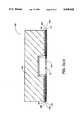
- FIG. 1ais a cross-sectional view of a TAB Grid Array (TGA) package 100 using TAB inner lead bonding, in an embodiment of the present invention.
- TGATAB Grid Array
- FIG. 1bis a partial cut-out view of TAB tape 103 of FIG. 1a.
- FIG. 1cis a partial cut-out view of the TGA package in FIG. 1a.
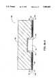
- FIG. 2ais a cross-sectional view of a TGA package 200 using wire bonding in a second embodiment of the present invention.
- FIG. 2bis a schematic view of the TAB tape 203 of FIG. 2a, which does not use the free-standing inner leads of TGA package 100.
- FIG. 3a-1,2,3,4summarize the steps in an assembly process for TGA package 100 shown in FIG. 1a.
- FIG. 3b-1,2,3,4,5summarize the steps in an assembly process for TGA package 200 shown in FIG. 2a.
- FIG. 1ashows a cross-sectional view of a TAB Grid Array (TGA) package 100 in an embodiment of the present invention.
- a semiconductor die 101having contacts 102 closely spaced at a pitch of 50 microns or wider, is encapsulated in a cavity 125 of a metallic heat spreader 106.
- Cavity 125is filled with an encapsulation material 104, which can be provided by an epoxy resin, as is known in the art.
- Semiconductor die 101is attached by a thin layer of thermally conductive epoxy 105 to heat spreader 106.
- TAB tape 103which comprises a signal trace and pad ("conductor") layer 103a held between two dielectric layers 109 and 110.
- Dielectric layer 109is attached to heat spreader 106 by a thin layer of adhesive 108.
- Heat spreader 106also provides support for TAB tape 103, thereby serving as a stiffener material for TAB tape 103.
- TGA package 100uses solder balls (e.g. solder balls 111 and 112) to electrically connect the integrated circuit to metallic traces on an external printed circuit board (PCB) 150 (not shown).
- PCBprinted circuit board
- Openings in dielectric layer 110allow electrical connections between the metallic traces on layer 103a of TAB tape 103 and metallic traces on external PCB 150.
- solder ball 112is used to make a connection between external PCB 150 and conductive pads in TAB tape 103 through an opening in dielectric layer 110.
- An another exampleis an opening 114, which opens through both dielectric layers 109 and 110 to provide a ground connection between external PCB 150 and heat spreader 106 via solder ball 113.
- TAB tape 103includes a 30-micron thick conductor layer 103a and, two 50-micron dielectric layers 109 and 110 on each side of conductor layer 103a.
- the partial cut-out view of FIG. 1bis a top view of TAB tape 103 with a corner of dielectric layer 109 removed, for the purpose of this illustration, to expose the conductor layer 103a.
- Conductor layer 103ahas a multitude of electrically conductive traces 119 that emanate radially from the center device hole area 120 to connect to an array 121 of conductive pads.
- the pitch of pad array 121can range between 600-1500 microns and the diameter of each pad can range between 100-750 microns, depending on the pin count required by the semiconductor die.
- Most of the pads in pad array 121are solid, e.g. pad 117, and are used for signal connections.
- Other pads, e.g. 114,have an aperture at the center and are used for ground connections.
- step 301the pads on the die are bonded to the free-standing tape traces, i.e. traces 119, via the conventional thermosonic or thermocompression TAB inner lead bonding techniques.
- TAB inner lead bonding techniquesare known in the industry, including the method disclosed in U.S. Pat. No. 4,842,662 to Jacobi, entitled “Bumpless Inner Lead Bonding", issued in Jun. 27, 1989, using bumpless thermosonic bonding on both the semiconductor die and the TAB tape.
- Dielectric layer 109which carries the conductive traces 119, is solid except at the locations of the ground pads in pad array 121. At a ground pad, dielectric layer 109 provides an aperture of the same size as the ground pad.
- Dielectric layer 110has an array of apertures coincident with the pads in pad array 121 of conductor layer 103a.
- Dielectric layers 109 and 110each have an inner aperture, shown in FIG. 1a at center device hole area 120. The inner aperture accepts the semiconductor die, but leaves a short length of the inner leads or traces 119 unsupported for bonding.
- FIG. 1cshows a partial cut-out view of FIG. 1a's TGA package 100.
- This partial cut-out viewexposes, for the purpose of illustration, cavity 125 of heat spreader 106.
- Heat spreader 106is made of a thermally conductive material, such as copper, to remove the power dissipated in the semiconductor die.
- Other suitable materialscan also be used for heat spreader 106.
- Such other materialsinclude copper/tungsten/copper and copper/molybdenum/copper laminates, beryllium oxide or metallized aluminum nitride.
- Aluminum nitridecan be metallized with chromium/gold, titanium/gold, nickel/gold films.
- heat spreader 106can be made of materials (e.g. aluminum) of larger TCE mismatch to silicon. As shown in FIGS. 1a and 1c, heat spreader 106 has a cavity 125 which encloses semiconductor die 101. In this embodiment, the downward-facing surface (i.e. the side open to cavity 125) of heat spreader 106 is plated with a coat of thin metal, e.g. silver or gold, that can be wetted by solder. This thin metal coat allows the ground solder balls to mechanically and electrically attach to heat spreader 106 after a reflow step.
- thin metale.g. silver or gold
- step 302the back surface of semiconductor die 101 is attached to the back wall of cavity 125 via a thermally conductive adhesive film 105.
- This thermally conductive adhesive film 105allows heat to be transferred by conduction from semiconductor die 101 to heat spreader 106.
- TAB tape 103is attached to the bottom surface of heat spreader 106 using an appropriate adhesive 124 that can withstand the conventional environmental stress tests usually performed on electronic packages.
- an adhesiveis similar to that used in bonding conductor layer 103a and dielectric layers 109 and 110 of TAB tape 103 itself.
- Die aperture 120 on TAB tape 103is aligned to cavity 125 with dielectric layer 109 secured on the bottom surface of heat spreader 106.
- the process steps for attaching semiconductor die 101 and for attaching TAB tape 103 to heat spreader 106are performed simultaneously at step 302 and cured simultaneously.
- Four optional posts, e.g. post 128 of FIG. 1c,are provided at the corners of heat spreader 106 to maintain a certain height of solder balls after a reflow step (see below).
- the inner lead bonds, the front side of semiconductor die 101, and the remaining space in heat spreader cavity 125,are filled with encapsulation material 104 at step 303.
- Encapsulation material 104is typically syringe-dispensed to enclose semiconductor die 101.
- the openings between inner leadsallow the encapsulant to flow and fill die cavity 125 completely leaving no voids.
- encapsulation material 104protects both the inner lead bonds and semiconductor die 101 from mechanical and environmental damages.
- the encapsulation materialis cured at 150° C. for three hours, during which the temperature is ramped three steps.
- solder ballsare attached onto the pads of pad array 121, which are exposed by the openings of dielectric layer 110.
- a fluxis first deposited on each solder ball.
- the solder ballsare placed using an appropriate pick-and-place equipment.
- the solder balls so placedare reflowed in place using a conventional infrared or hot air reflow equipment and process, heating the solder balls to above 200° C.
- the excess fluxis then removed by cleaning TGA package 100 with an appropriate cleaning agent, e.g. a water-based cleaning agent.
- solder balls placed on the pads of pad array 121 with apertures in dielectric layer 109are reflowed on heat spreader 106, thereby directly establishing a ground connection between the solder ball and heat spreader 106.
- the solder balls placed on the solid pads of pad array 121are connected to the device pads only and provide signal and power connections between the solder balls and traces 119 of the TAB tape.
- the inner lead bondsprovide connection to the corresponding pads of the semiconductor die 101.
- TGA package 100is then dry baked at 120° C. for at least one hour.
- TGA package 100can then be assembled to an external PCB using a suitable conventional surface mount process and equipment.
- An example of such conventional surface mount processdispenses solder paste on connection pads of the PCB, aligns the solder balls on TGA package 100 to these connection pads of the PCB, and reflows the solder balls to establish the desired mechanical and electrical bonds with the PCB.
- the present embodimentuses a single-metal TAB tape 103, which is capable of delivering frequency performance of 100 MHz or above. Further, single-metal tape 103 and electrically conductive heat spreader 106 form a controlled impedance electrical path for signals and minimize uncompensated trace inductance. Such performance is usually only achievable in a relatively higher cost two-metal tape. Because TAB tape 103 can connect to semiconductor die 101 and the external PCB is done on the same side of TAB tape 103, shorter traces result. Further, trace looping from the back side of substrate to the front, as required in a conventional BGA package, is also avoided. The combined result of same-side connection and short traces translate to a much smaller inductance than that of a conventional BGA package.
- the present embodimentachieves a smaller pitch than that achieved by wire bonding, thereby allowing a smaller die to be designed for a pad-limited IC.
- a smaller die sizemeans lower cost of production.
- an electrical connection between the semiconductor die and the external PCB boardis achieved using only two connections rather than four connections required of a conventional BGA package. A smaller number of connections increases assembly yield and package reliability.
- the TAB tape of a TGA packageabsorbs significantly less moisture than a conventional BGA package, leading to a higher reliability package not susceptible to the "popcorn" failure mode common in the PCB based BGA packages.
- the thermal dissipation capacity of a TGA package of the present inventionis significantly greater than a BGA package.
- Such a TGA packagecan handle a semiconductor die dissipating power up to 10 watts without using a heat sink.
- a heat sinkis used with the TGA package of the present invention, power in excess of 25 watts can be handled under forced air conditions.
- This thermal dissipation capacityrepresents a junction-to-case thermal impedance of less than 0.4° C./watt, which is achieved because the semiconductor die is directly attached to the heat spreader using a thermally conductive epoxy.
- FIGS. 2a and 2bA TGA package 200 in an alternative embodiment is shown in FIGS. 2a and 2b.
- FIG. 2ais a cross sectional view of TGA package 200
- FIG. 2bis a partially cut-out top view of TAB tape 203 in TGA package 200.
- TGA package 200is substantially the same as TGA package 100 of FIG. 1 except for the differences described below. To facilitate cross reference between TGA packages 100 and 200, the same reference numerals are used to indicate substantially identical features.
- TGA package 200the pads on pad array 121 are connected to traces on a TAB tape 203 using a wire bonding technique, rather than a TAB inner lead bonding technique.
- Wire bonds 210a and 210b in FIG. 2aare illustrative.
- TAB tape aperture 220 (FIG. 2b) fop semiconductor die 101is slightly larger than die cavity 125 in heat spreader 106, thereby exposing a narrow perimeter of heat spreader 106 surrounding cavity 125.
- wire bondingis used to provide ground connections directly from semiconductor die 101 to heat spreader 106 by a wire bond 210b to the rim of heat spreader 106 surrounding cavity 125.
- dielectric layer 109 of TGA package 200protects traces 119 right up to die aperture 220, hence providing the mechanical support to metal trace 119, so as to establish necessary support for wire bonding.
- FIG. 3bshows an assembly process for TGA package 200.
- TAB tape 203is attached to heat spreader 106 using an adhesive film 124, which is described above with respect to the assembly process of FIG. 3a.
- adhesive film 124is cured, semiconductor die 101 is attached in cavity 125 using a thermally conductive epoxy 105, which is also described above.
- step 353after conductive epoxy 105 is cured, pads on semiconductor die 101 are wire bonded to traces 119 on TAB tape 203. At this step also, a ground pad on semiconductor die 101 is wire bonded to heat spreader 106 at the periphery of die aperture 220 of TAB tape 203. This wire bond is shown in FIG. 2b as wire bond 210b.
- an encapsulation materialis syringe-dispensed to form encapsulation 104 filling cavity 125 and covering both semiconductor die 101 and the wire bonds. Encapsulation 104 of TGA package 200 is allowed to cure in the same way as the corresponding encapsulation in TGA package 100. Solder balls are attached at step 355. Step 355 is substantially identical as step 304 shown in FIG. 3a in the assembly process of TGA package 100.
- TGA packages 100 and 200stems from the wire bondings in TGA package 200.
- Wire bondings in TGA package 200cannot achieve the fine pitch achieved in TAB inner lead bonding of TGA package 100. Consequently, a pad-limited semiconductor die designed for wire bonding is likely to be larger and more expensive to produce. Also, since the uncompensated impedance of a wire bond is larger than a corresponding TAB inner lead bond, the high-end frequency performance of TGA package 200 is lower than the corresponding frequency performance of TGA package 100.
Landscapes
- Engineering & Computer Science (AREA)
- Microelectronics & Electronic Packaging (AREA)
- Physics & Mathematics (AREA)
- Condensed Matter Physics & Semiconductors (AREA)
- General Physics & Mathematics (AREA)
- Computer Hardware Design (AREA)
- Power Engineering (AREA)
- Wire Bonding (AREA)
Abstract
Description
Claims (7)
Priority Applications (1)
| Application Number | Priority Date | Filing Date | Title |
|---|---|---|---|
| US08/201,869US5409865A (en) | 1993-09-03 | 1994-02-25 | Process for assembling a TAB grid array package for an integrated circuit |
Applications Claiming Priority (3)
| Application Number | Priority Date | Filing Date | Title |
|---|---|---|---|
| US08/116,944US5397921A (en) | 1993-09-03 | 1993-09-03 | Tab grid array |
| US08/201,869US5409865A (en) | 1993-09-03 | 1994-02-25 | Process for assembling a TAB grid array package for an integrated circuit |
| EP94309762AEP0718882A1 (en) | 1993-09-03 | 1994-12-23 | Tab grid array for a semiconductor device |
Related Parent Applications (1)
| Application Number | Title | Priority Date | Filing Date |
|---|---|---|---|
| US08/116,944DivisionUS5397921A (en) | 1993-09-03 | 1993-09-03 | Tab grid array |
Publications (1)
| Publication Number | Publication Date |
|---|---|
| US5409865Atrue US5409865A (en) | 1995-04-25 |
Family
ID=26137458
Family Applications (2)
| Application Number | Title | Priority Date | Filing Date |
|---|---|---|---|
| US08/116,944Expired - LifetimeUS5397921A (en) | 1993-09-03 | 1993-09-03 | Tab grid array |
| US08/201,869Expired - LifetimeUS5409865A (en) | 1993-09-03 | 1994-02-25 | Process for assembling a TAB grid array package for an integrated circuit |
Family Applications Before (1)
| Application Number | Title | Priority Date | Filing Date |
|---|---|---|---|
| US08/116,944Expired - LifetimeUS5397921A (en) | 1993-09-03 | 1993-09-03 | Tab grid array |
Country Status (2)
| Country | Link |
|---|---|
| US (2) | US5397921A (en) |
| EP (1) | EP0718882A1 (en) |
Cited By (161)
| Publication number | Priority date | Publication date | Assignee | Title |
|---|---|---|---|---|
| US5474957A (en)* | 1994-05-09 | 1995-12-12 | Nec Corporation | Process of mounting tape automated bonded semiconductor chip on printed circuit board through bumps |
| US5572405A (en)* | 1995-06-07 | 1996-11-05 | International Business Machines Corporation (Ibm) | Thermally enhanced ball grid array package |
| US5586010A (en)* | 1995-03-13 | 1996-12-17 | Texas Instruments Incorporated | Low stress ball grid array package |
| WO1997004629A1 (en)* | 1995-07-14 | 1997-02-06 | Olin Corporation | Metal ball grid electronic package |
| US5602059A (en)* | 1994-09-08 | 1997-02-11 | Shinko Electric Industries Co., Ltd. | Semiconductor device and method for manufacturing same |
| US5663593A (en)* | 1995-10-17 | 1997-09-02 | National Semiconductor Corporation | Ball grid array package with lead frame |
| US5710695A (en)* | 1995-11-07 | 1998-01-20 | Vlsi Technology, Inc. | Leadframe ball grid array package |
| US5717252A (en)* | 1994-07-25 | 1998-02-10 | Mitsui High-Tec, Inc. | Solder-ball connected semiconductor device with a recessed chip mounting area |
| US5723369A (en)* | 1996-03-14 | 1998-03-03 | Lsi Logic Corporation | Method of flip chip assembly |
| US5724230A (en)* | 1996-06-21 | 1998-03-03 | International Business Machines Corporation | Flexible laminate module including spacers embedded in an adhesive |
| US5724232A (en)* | 1995-02-15 | 1998-03-03 | International Business Machines Corporation | Chip carrier having an organic photopatternable material and a metal substrate |
| US5726482A (en) | 1994-02-08 | 1998-03-10 | Prolinx Labs Corporation | Device-under-test card for a burn-in board |
| US5728606A (en)* | 1995-01-25 | 1998-03-17 | International Business Machines Corporation | Electronic Package |
| US5729051A (en)* | 1994-09-22 | 1998-03-17 | Nec Corporation | Tape automated bonding type semiconductor device |
| US5763952A (en)* | 1992-06-04 | 1998-06-09 | Lsi Logic Corporation | Multi-layer tape having distinct signal, power and ground planes, semiconductor device assembly employing same, apparatus for and method of assembling same |
| WO1998025301A1 (en)* | 1996-12-02 | 1998-06-11 | Minnesota Mining And Manufacturing Company | Tab tape ball grid array package with vias laterally offset from solder ball bond sites |
| US5767528A (en)* | 1996-02-20 | 1998-06-16 | Fujitsu Limited | Semiconductor device including pad portion for testing |
| US5767575A (en) | 1995-10-17 | 1998-06-16 | Prolinx Labs Corporation | Ball grid array structure and method for packaging an integrated circuit chip |
| EP0788159A3 (en)* | 1996-01-31 | 1998-06-17 | Lsi Logic Corporation | Microelectronic integrated circuit mounted on circuit board with solder column interconnection |
| US5776796A (en)* | 1994-05-19 | 1998-07-07 | Tessera, Inc. | Method of encapsulating a semiconductor package |
| US5789809A (en)* | 1995-08-22 | 1998-08-04 | National Semiconductor Corporation | Thermally enhanced micro-ball grid array package |
| US5808351A (en) | 1994-02-08 | 1998-09-15 | Prolinx Labs Corporation | Programmable/reprogramable structure using fuses and antifuses |
| US5834824A (en) | 1994-02-08 | 1998-11-10 | Prolinx Labs Corporation | Use of conductive particles in a nonconductive body as an integrated circuit antifuse |
| US5834336A (en)* | 1996-03-12 | 1998-11-10 | Texas Instruments Incorporated | Backside encapsulation of tape automated bonding device |
| US5843808A (en)* | 1996-01-11 | 1998-12-01 | Asat, Limited | Structure and method for automated assembly of a tab grid array package |
| US5854085A (en)* | 1992-06-04 | 1998-12-29 | Lsi Logic Corporation | Multi-layer tab tape having distinct signal, power and ground planes, semiconductor device assembly employing same, apparatus for and method of assembling same |
| US5872338A (en) | 1996-04-10 | 1999-02-16 | Prolinx Labs Corporation | Multilayer board having insulating isolation rings |
| US5873162A (en)* | 1997-02-11 | 1999-02-23 | International Business Machines Corporation | Technique for attaching a stiffener to a flexible substrate |
| US5884396A (en)* | 1997-05-01 | 1999-03-23 | Compeq Manufacturing Company, Limited | Transfer flat type ball grid array method for manufacturing packaging substrate |
| US5886399A (en)* | 1995-09-20 | 1999-03-23 | Sony Corporation | Lead frame and integrated circuit package |
| US5906043A (en) | 1995-01-18 | 1999-05-25 | Prolinx Labs Corporation | Programmable/reprogrammable structure using fuses and antifuses |
| US5906042A (en) | 1995-10-04 | 1999-05-25 | Prolinx Labs Corporation | Method and structure to interconnect traces of two conductive layers in a printed circuit board |
| US5909057A (en)* | 1997-09-23 | 1999-06-01 | Lsi Logic Corporation | Integrated heat spreader/stiffener with apertures for semiconductor package |
| US5917229A (en) | 1994-02-08 | 1999-06-29 | Prolinx Labs Corporation | Programmable/reprogrammable printed circuit board using fuse and/or antifuse as interconnect |
| US5929517A (en)* | 1994-12-29 | 1999-07-27 | Tessera, Inc. | Compliant integrated circuit package and method of fabricating the same |
| US5956232A (en)* | 1995-01-12 | 1999-09-21 | Fraunhofer-Gesellschaft Zur Forderung Der Angewandten Forschung E.V. | Chip support arrangement and chip support for the manufacture of a chip casing |
| US5966803A (en)* | 1996-05-31 | 1999-10-19 | International Business Machines Corporation | Ball grid array having no through holes or via interconnections |
| US5972734A (en)* | 1997-09-17 | 1999-10-26 | Lsi Logic Corporation | Interposer for ball grid array (BGA) package |
| US5985695A (en)* | 1996-04-24 | 1999-11-16 | Amkor Technology, Inc. | Method of making a molded flex circuit ball grid array |
| US5994773A (en)* | 1996-03-06 | 1999-11-30 | Hirakawa; Tadashi | Ball grid array semiconductor package |
| US6002171A (en)* | 1997-09-22 | 1999-12-14 | Lsi Logic Corporation | Integrated heat spreader/stiffener assembly and method of assembly for semiconductor package |
| US6020221A (en)* | 1996-12-12 | 2000-02-01 | Lsi Logic Corporation | Process for manufacturing a semiconductor device having a stiffener member |
| US6034427A (en) | 1998-01-28 | 2000-03-07 | Prolinx Labs Corporation | Ball grid array structure and method for packaging an integrated circuit chip |
| US6048755A (en)* | 1998-11-12 | 2000-04-11 | Micron Technology, Inc. | Method for fabricating BGA package using substrate with patterned solder mask open in die attach area |
| US6057594A (en)* | 1997-04-23 | 2000-05-02 | Lsi Logic Corporation | High power dissipating tape ball grid array package |
| US6064286A (en)* | 1998-07-31 | 2000-05-16 | The Whitaker Corporation | Millimeter wave module with an interconnect from an interior cavity |
| US6074898A (en)* | 1996-09-18 | 2000-06-13 | Sony Corporation | Lead frame and integrated circuit package |
| US6078097A (en)* | 1994-11-22 | 2000-06-20 | Sony Corporation | Lead frame |
| US6084777A (en)* | 1997-04-23 | 2000-07-04 | Texas Instruments Incorporated | Ball grid array package |
| US6084297A (en)* | 1998-09-03 | 2000-07-04 | Micron Technology, Inc. | Cavity ball grid array apparatus |
| US6104091A (en)* | 1996-05-24 | 2000-08-15 | Sony Corporation | Semiconductor package and the manufacturing method |
| US6107683A (en)* | 1997-06-20 | 2000-08-22 | Substrate Technologies Incorporated | Sequentially built integrated circuit package |
| US6145365A (en)* | 1997-09-29 | 2000-11-14 | Nakamura Seisakusho Kabushikigaisha | Method for forming a recess portion on a metal plate |
| US6160311A (en)* | 1999-06-14 | 2000-12-12 | First International Computer Inc. | Enhanced heat dissipating chip scale package method and devices |
| US6160705A (en)* | 1997-05-09 | 2000-12-12 | Texas Instruments Incorporated | Ball grid array package and method using enhanced power and ground distribution circuitry |
| US6166434A (en)* | 1997-09-23 | 2000-12-26 | Lsi Logic Corporation | Die clip assembly for semiconductor package |
| US6175497B1 (en)* | 1998-09-30 | 2001-01-16 | World Wiser Electronics Inc. | Thermal vias-provided cavity-down IC package structure |
| US6181977B1 (en)* | 1997-03-06 | 2001-01-30 | International Business Machines Corporation | Control for technique of attaching a stiffener to a flexible substrate |
| US6214640B1 (en) | 1999-02-10 | 2001-04-10 | Tessera, Inc. | Method of manufacturing a plurality of semiconductor packages |
| US6225686B1 (en)* | 1996-11-21 | 2001-05-01 | Sony Corporation | Semiconductor device |
| US6232666B1 (en) | 1998-12-04 | 2001-05-15 | Mciron Technology, Inc. | Interconnect for packaging semiconductor dice and fabricating BGA packages |
| US6305074B1 (en)* | 1996-06-13 | 2001-10-23 | Bull, S.A. | Support for integrated circuit and process for mounting an integrated circuit on a support |
| US6310390B1 (en) | 1999-04-08 | 2001-10-30 | Micron Technology, Inc. | BGA package and method of fabrication |
| US6355199B1 (en)* | 1999-02-12 | 2002-03-12 | St. Assembly Test Services Pte Ltd | Method of molding flexible circuit with molded stiffener |
| US6396141B2 (en) | 1998-10-14 | 2002-05-28 | 3M Innovative Properties Company | Tape ball grid array with interconnected ground plane |
| US20020064901A1 (en)* | 1996-03-22 | 2002-05-30 | Chuichi Miyazaki | Semiconductor device and manufacturing method thereof |
| US6404048B2 (en)* | 1998-09-03 | 2002-06-11 | Micron Technology, Inc. | Heat dissipating microelectronic package |
| US20020070443A1 (en)* | 2000-12-08 | 2002-06-13 | Xiao-Chun Mu | Microelectronic package having an integrated heat sink and build-up layers |
| WO2002049103A2 (en) | 2000-12-15 | 2002-06-20 | Intel Corporation | Microelectronic package having bumpless laminated interconnection layer |
| US20020079562A1 (en)* | 2000-12-22 | 2002-06-27 | Broadcom Corporation | Enhanced die-up ball grid array packages and method for making the same |
| US6429048B1 (en) | 2000-12-05 | 2002-08-06 | Asat Ltd. | Metal foil laminated IC package |
| US20020109226A1 (en)* | 2001-02-15 | 2002-08-15 | Broadcom Corporation | Enhanced die-down ball grid array and method for making the same |
| US20020135065A1 (en)* | 2000-12-01 | 2002-09-26 | Zhao Sam Ziqun | Thermally and electrically enhanced ball grid array packaging |
| US20020140083A1 (en)* | 2001-03-27 | 2002-10-03 | Nec Corporation | Semiconductor device haivng resin-sealed area on circuit board thereof |
| US6469897B2 (en)* | 2001-01-30 | 2002-10-22 | Siliconware Precision Industries Co., Ltd. | Cavity-down tape ball grid array package assembly with grounded heat sink and method of fabricating the same |
| US20020164838A1 (en)* | 2001-05-02 | 2002-11-07 | Moon Ow Chee | Flexible ball grid array chip scale packages and methods of fabrication |
| US20020171144A1 (en)* | 2001-05-07 | 2002-11-21 | Broadcom Corporation | Die-up ball grid array package with a heat spreader and method for making the same |
| US20020185734A1 (en)* | 2000-12-22 | 2002-12-12 | Zhao Sam Ziqun | Die-up ball grid array package with printed circuit board attachable heat spreader |
| US6537857B2 (en)* | 2001-05-07 | 2003-03-25 | St Assembly Test Service Ltd. | Enhanced BGA grounded heatsink |
| US6544812B1 (en) | 2000-11-06 | 2003-04-08 | St Assembly Test Service Ltd. | Single unit automated assembly of flex enhanced ball grid array packages |
| US6549413B2 (en) | 2001-02-27 | 2003-04-15 | Chippac, Inc. | Tape ball grid array semiconductor package structure and assembly process |
| EP1304739A1 (en)* | 2001-10-15 | 2003-04-23 | United Test Center Inc. | Semiconductor device and method for fabricating the same |
| US6562661B2 (en) | 2000-02-24 | 2003-05-13 | Micron Technology, Inc. | Tape stiffener, semiconductor device component assemblies including same, and stereolithographic methods for fabricating same |
| US20030107118A1 (en)* | 2001-10-09 | 2003-06-12 | Tessera, Inc. | Stacked packages |
| US20030122223A1 (en)* | 1998-04-02 | 2003-07-03 | Akio Nakamura | Semiconductor device in a recess of a semiconductor plate |
| US20030134450A1 (en)* | 2002-01-09 | 2003-07-17 | Lee Teck Kheng | Elimination of RDL using tape base flip chip on flex for die stacking |
| US20030146509A1 (en)* | 2002-02-01 | 2003-08-07 | Broadcom Corporation | Ball grid array package with separated stiffener layer |
| US20030146503A1 (en)* | 2002-02-01 | 2003-08-07 | Broadcom Corporation | Ball grid array package with stepped stiffener layer |
| US20030151143A1 (en)* | 2002-02-14 | 2003-08-14 | Macronix International Co., Ltd. | Semiconductor packaging device and manufacture thereof |
| US6614123B2 (en) | 2001-07-31 | 2003-09-02 | Chippac, Inc. | Plastic ball grid array package with integral heatsink |
| US20030164551A1 (en)* | 2002-03-04 | 2003-09-04 | Lee Teck Kheng | Method and apparatus for flip-chip packaging providing testing capability |
| US20030164548A1 (en)* | 2002-03-04 | 2003-09-04 | Lee Teck Kheng | Flip chip packaging using recessed interposer terminals |
| US20030166312A1 (en)* | 2002-03-04 | 2003-09-04 | Lee Teck Kheng | Methods for assembly and packaging of flip chip configured dice with interposer |
| US20030164540A1 (en)* | 2002-03-04 | 2003-09-04 | Lee Teck Kheng | Semiconductor die packages with recessed interconnecting structures and methods for assembling the same |
| US20030164543A1 (en)* | 2002-03-04 | 2003-09-04 | Teck Kheng Lee | Interposer configured to reduce the profiles of semiconductor device assemblies and packages including the same and methods |
| US20030179549A1 (en)* | 2002-03-22 | 2003-09-25 | Zhong Chong Hua | Low voltage drop and high thermal perfor mance ball grid array package |
| US20030178719A1 (en)* | 2002-03-22 | 2003-09-25 | Combs Edward G. | Enhanced thermal dissipation integrated circuit package and method of manufacturing enhanced thermal dissipation integrated circuit package |
| US20030193091A1 (en)* | 2002-04-16 | 2003-10-16 | Yu Chan Min | Semiconductor packages with leadframe grid arrays and components and methods for making the same |
| US20030197256A1 (en)* | 2000-02-24 | 2003-10-23 | Richard Pommer | Power conditioning substrate stiffener |
| US6650015B2 (en) | 2002-02-05 | 2003-11-18 | Siliconware Precision Industries Co., Ltd. | Cavity-down ball grid array package with semiconductor chip solder ball |
| US6664617B2 (en) | 2000-12-19 | 2003-12-16 | Convergence Technologies, Ltd. | Semiconductor package |
| US20030230800A1 (en)* | 2002-05-28 | 2003-12-18 | Fujitsu Limited | Semiconductor device manufacturing method, semiconductor device, and semiconductor device unit |
| US20040031972A1 (en)* | 2001-10-09 | 2004-02-19 | Tessera, Inc. | Stacked packages |
| US20040036158A1 (en)* | 2002-08-26 | 2004-02-26 | Hiroki Tanaka | Tab tape, method of making same and semiconductor device |
| US6706563B2 (en) | 2002-04-10 | 2004-03-16 | St Assembly Test Services Pte Ltd | Heat spreader interconnect methodology for thermally enhanced PBGA packages |
| US6709898B1 (en)* | 2000-10-04 | 2004-03-23 | Intel Corporation | Die-in-heat spreader microelectronic package |
| US20040061220A1 (en)* | 1996-03-22 | 2004-04-01 | Chuichi Miyazaki | Semiconductor device and manufacturing method thereof |
| US20040113284A1 (en)* | 2002-03-21 | 2004-06-17 | Broadcom Corporation | Method for making an enhanced die-up ball grid array package with two substrates |
| US6756251B2 (en) | 2001-08-21 | 2004-06-29 | Micron Technology, Inc. | Method of manufacturing microelectronic devices, including methods of underfilling microelectronic components through an underfill aperture |
| US20040159957A1 (en)* | 2002-03-04 | 2004-08-19 | Lee Teck Kheng | Interposer substrate and wafer scale interposer substrate member for use with flip-chip configured semiconductor dice |
| US6790710B2 (en) | 2002-01-31 | 2004-09-14 | Asat Limited | Method of manufacturing an integrated circuit package |
| US20040195701A1 (en)* | 2003-01-07 | 2004-10-07 | Attarwala Abbas Ismail | Electronic package and method |
| US20040195685A1 (en)* | 2003-04-02 | 2004-10-07 | Stmicroelectronics, Inc. | System and method for venting pressure from an integrated circuit package sealed with a lid |
| US20040198033A1 (en)* | 2002-08-20 | 2004-10-07 | Lee Teck Kheng | Double bumping of flexible substrate for first and second level interconnects |
| US20040214373A1 (en)* | 2003-04-22 | 2004-10-28 | Tongbi Jiang | Packaged microelectronic devices and methods for packaging microelectronic devices |
| US20040212051A1 (en)* | 2000-12-22 | 2004-10-28 | Broadcom Corporation | Ball grid array package with patterned stiffener layer |
| US20040216864A1 (en)* | 2003-04-30 | 2004-11-04 | Wong Marvin Glenn | CTE matched application specific heat sink assembly |
| US6825108B2 (en) | 2002-02-01 | 2004-11-30 | Broadcom Corporation | Ball grid array package fabrication with IC die support structures |
| US20050023651A1 (en)* | 2003-08-01 | 2005-02-03 | Kim Dalson Ye Seng | Semiconductor component having chip on board leadframe and method of fabrication |
| US6861750B2 (en) | 2002-02-01 | 2005-03-01 | Broadcom Corporation | Ball grid array package with multiple interposers |
| US20050062149A1 (en)* | 2001-06-26 | 2005-03-24 | Chippac, Inc | Integral heatsink ball grid array |
| US20050062173A1 (en)* | 2000-08-16 | 2005-03-24 | Intel Corporation | Microelectronic substrates with integrated devices |
| US20050098900A1 (en)* | 2003-06-13 | 2005-05-12 | Delphi Technologies, Inc. | Relaxed tolerance flip chip assembly |
| US20050116326A1 (en)* | 2003-10-06 | 2005-06-02 | Tessera, Inc. | Formation of circuitry with modification of feature height |
| US20050167850A1 (en)* | 1995-12-19 | 2005-08-04 | Moden Walter L. | Flip-chip adaptor package for bare die |
| US20050173805A1 (en)* | 2003-12-30 | 2005-08-11 | Tessera, Inc. | Micro pin grid array with pin motion isolation |
| US20050173796A1 (en)* | 2001-10-09 | 2005-08-11 | Tessera, Inc. | Microelectronic assembly having array including passive elements and interconnects |
| US20050181655A1 (en)* | 2003-12-30 | 2005-08-18 | Tessera, Inc. | Micro pin grid array with wiping action |
| US20050280141A1 (en)* | 2004-06-21 | 2005-12-22 | Broadcom Corporation | Integrated circuit device package having both wire bond and flip-chip interconnections and method of making the same |
| US20050280139A1 (en)* | 2004-06-21 | 2005-12-22 | Broadcom Corporation | Multipiece apparatus for thermal and electromagnetic interference (EMI) shielding enhancement in die-up array packages and method of making the same |
| US20050284658A1 (en)* | 2003-10-06 | 2005-12-29 | Tessera, Inc. | Components with posts and pads |
| US20060055038A1 (en)* | 2004-09-10 | 2006-03-16 | Jinghui Mu | Tape ball grid array package with electromagnetic interference protection and method for fabricating the package |
| US20060065972A1 (en)* | 2004-09-29 | 2006-03-30 | Broadcom Corporation | Die down ball grid array packages and method for making same |
| US20060084254A1 (en)* | 2004-01-06 | 2006-04-20 | Attarwala Abbas I | Method for making electronic packages |
| US20060267184A1 (en)* | 1997-07-02 | 2006-11-30 | Kinsman Larry D | Varied-thickness heat sink for integrated circuit (IC) package |
| US7161239B2 (en) | 2000-12-22 | 2007-01-09 | Broadcom Corporation | Ball grid array package enhanced with a thermal and electrical connector |
| US20070267734A1 (en)* | 2006-05-16 | 2007-11-22 | Broadcom Corporation | No-lead IC packages having integrated heat spreader for electromagnetic interference (EMI) shielding and thermal enhancement |
| US20080003402A1 (en)* | 2003-10-06 | 2008-01-03 | Tessera, Inc. | Fine pitch microcontacts and method for forming thereof |
| US7405145B2 (en) | 2001-12-18 | 2008-07-29 | Broadcom Corporation | Ball grid array package substrates with a modified central opening and method for making the same |
| US7432586B2 (en) | 2004-06-21 | 2008-10-07 | Broadcom Corporation | Apparatus and method for thermal and electromagnetic interference (EMI) shielding enhancement in die-up array packages |
| US7537958B1 (en)* | 1998-08-05 | 2009-05-26 | Fairchild Semiconductor Corporation | High performance multi-chip flip chip package |
| US20090197114A1 (en)* | 2007-01-30 | 2009-08-06 | Da-Yuan Shih | Modification of pb-free solder alloy compositions to improve interlayer dielectric delamination in silicon devices and electromigration resistance in solder joints |
| US20090197103A1 (en)* | 2007-01-30 | 2009-08-06 | Da-Yuan Shih | Modification of pb-free solder alloy compositions to improve interlayer dielectric delamination in silicon devices and electromigration resistance in solder joints |
| US7611981B1 (en)* | 1997-05-09 | 2009-11-03 | Texas Instruments Incorporated | Optimized circuit design layout for high performance ball grid array packages |
| US20100044860A1 (en)* | 2008-08-21 | 2010-02-25 | Tessera Interconnect Materials, Inc. | Microelectronic substrate or element having conductive pads and metal posts joined thereto using bond layer |
| US20100265665A1 (en)* | 2009-04-15 | 2010-10-21 | Yukihiro Kozaka | Electronic device having a heat sink |
| US20110116242A1 (en)* | 2009-11-18 | 2011-05-19 | Seagate Technology Llc | Tamper evident pcba film |
| US20110235304A1 (en)* | 2010-03-23 | 2011-09-29 | Alcatel-Lucent Canada, Inc. | Ic package stiffener with beam |
| USRE43112E1 (en) | 1998-05-04 | 2012-01-17 | Round Rock Research, Llc | Stackable ball grid array package |
| USRE43404E1 (en) | 1996-03-07 | 2012-05-22 | Tessera, Inc. | Methods for providing void-free layer for semiconductor assemblies |
| US8330272B2 (en) | 2010-07-08 | 2012-12-11 | Tessera, Inc. | Microelectronic packages with dual or multiple-etched flip-chip connectors |
| US8580607B2 (en) | 2010-07-27 | 2013-11-12 | Tessera, Inc. | Microelectronic packages with nanoparticle joining |
| US8853558B2 (en) | 2010-12-10 | 2014-10-07 | Tessera, Inc. | Interconnect structure |
| US8884448B2 (en) | 2007-09-28 | 2014-11-11 | Tessera, Inc. | Flip chip interconnection with double post |
| US8921994B2 (en) | 2012-09-14 | 2014-12-30 | Freescale Semiconductor, Inc. | Thermally enhanced package with lid heat spreader |
| US9010616B2 (en)* | 2011-05-31 | 2015-04-21 | Indium Corporation | Low void solder joint for multiple reflow applications |
| US9159643B2 (en) | 2012-09-14 | 2015-10-13 | Freescale Semiconductor, Inc. | Matrix lid heatspreader for flip chip package |
| US9633971B2 (en) | 2015-07-10 | 2017-04-25 | Invensas Corporation | Structures and methods for low temperature bonding using nanoparticles |
| US10535626B2 (en) | 2015-07-10 | 2020-01-14 | Invensas Corporation | Structures and methods for low temperature bonding using nanoparticles |
| US11973056B2 (en) | 2016-10-27 | 2024-04-30 | Adeia Semiconductor Technologies Llc | Methods for low temperature bonding using nanoparticles |
| US12211809B2 (en) | 2020-12-30 | 2025-01-28 | Adeia Semiconductor Bonding Technologies Inc. | Structure with conductive feature and method of forming same |
Families Citing this family (161)
| Publication number | Priority date | Publication date | Assignee | Title |
|---|---|---|---|---|
| US5629835A (en)* | 1994-07-19 | 1997-05-13 | Olin Corporation | Metal ball grid array package with improved thermal conductivity |
| US5539153A (en)* | 1994-08-08 | 1996-07-23 | Hewlett-Packard Company | Method of bumping substrates by contained paste deposition |
| JP2595909B2 (en)* | 1994-09-14 | 1997-04-02 | 日本電気株式会社 | Semiconductor device |
| US5541450A (en)* | 1994-11-02 | 1996-07-30 | Motorola, Inc. | Low-profile ball-grid array semiconductor package |
| US5715144A (en)* | 1994-12-30 | 1998-02-03 | International Business Machines Corporation | Multi-layer, multi-chip pyramid and circuit board structure |
| US5677566A (en) | 1995-05-08 | 1997-10-14 | Micron Technology, Inc. | Semiconductor chip package |
| JP3093960B2 (en)* | 1995-07-06 | 2000-10-03 | 株式会社三井ハイテック | Method for manufacturing semiconductor circuit element mounting substrate frame |
| GB9515651D0 (en)* | 1995-07-31 | 1995-09-27 | Sgs Thomson Microelectronics | A method of manufacturing a ball grid array package |
| US5663530A (en)* | 1995-08-01 | 1997-09-02 | Minnesota Mining And Manufacturing Company | Wire bond tape ball grid array package |
| DE19546045C1 (en)* | 1995-12-09 | 1997-05-22 | Bosch Gmbh Robert | Flip-chip method for producing a multichip module |
| KR0179802B1 (en)* | 1995-12-29 | 1999-03-20 | 문정환 | Semiconductor package |
| US5760465A (en)* | 1996-02-01 | 1998-06-02 | International Business Machines Corporation | Electronic package with strain relief means |
| KR100192760B1 (en)* | 1996-02-29 | 1999-06-15 | 황인길 | Method for manufacturing a BAG semiconductor package using a metal carrier frame and the semiconductor package |
| US5907903A (en)* | 1996-05-24 | 1999-06-01 | International Business Machines Corporation | Multi-layer-multi-chip pyramid and circuit board structure and method of forming same |
| US6395991B1 (en) | 1996-07-29 | 2002-05-28 | International Business Machines Corporation | Column grid array substrate attachment with heat sink stress relief |
| JP2825084B2 (en)* | 1996-08-29 | 1998-11-18 | 日本電気株式会社 | Semiconductor device and manufacturing method thereof |
| KR100544033B1 (en)* | 1996-09-30 | 2006-01-23 | 지멘스 악티엔게젤샤프트 | Microelectronic component with a sandwich design |
| US5796169A (en)* | 1996-11-19 | 1998-08-18 | International Business Machines Corporation | Structurally reinforced ball grid array semiconductor package and systems |
| US5990545A (en)* | 1996-12-02 | 1999-11-23 | 3M Innovative Properties Company | Chip scale ball grid array for integrated circuit package |
| US5866949A (en)* | 1996-12-02 | 1999-02-02 | Minnesota Mining And Manufacturing Company | Chip scale ball grid array for integrated circuit packaging |
| US6323065B1 (en) | 1997-05-07 | 2001-11-27 | Signetics | Methods for manufacturing ball grid array assembly semiconductor packages |
| US6020637A (en)* | 1997-05-07 | 2000-02-01 | Signetics Kp Co., Ltd. | Ball grid array semiconductor package |
| US6395582B1 (en) | 1997-07-14 | 2002-05-28 | Signetics | Methods for forming ground vias in semiconductor packages |
| US6060341A (en)* | 1998-01-12 | 2000-05-09 | International Business Machines Corporation | Method of making an electronic package |
| US6053394A (en)* | 1998-01-13 | 2000-04-25 | International Business Machines Corporation | Column grid array substrate attachment with heat sink stress relief |
| US6552264B2 (en)* | 1998-03-11 | 2003-04-22 | International Business Machines Corporation | High performance chip packaging and method |
| SG75841A1 (en)* | 1998-05-02 | 2000-10-24 | Eriston Invest Pte Ltd | Flip chip assembly with via interconnection |
| US6406939B1 (en) | 1998-05-02 | 2002-06-18 | Charles W. C. Lin | Flip chip assembly with via interconnection |
| US6423623B1 (en) | 1998-06-09 | 2002-07-23 | Fairchild Semiconductor Corporation | Low Resistance package for semiconductor devices |
| US6057601A (en)* | 1998-11-27 | 2000-05-02 | Express Packaging Systems, Inc. | Heat spreader with a placement recess and bottom saw-teeth for connection to ground planes on a thin two-sided single-core BGA substrate |
| TW522536B (en) | 1998-12-17 | 2003-03-01 | Wen-Chiang Lin | Bumpless flip chip assembly with strips-in-via and plating |
| SG82591A1 (en) | 1998-12-17 | 2001-08-21 | Eriston Technologies Pte Ltd | Bumpless flip chip assembly with solder via |
| SG82590A1 (en) | 1998-12-17 | 2001-08-21 | Eriston Technologies Pte Ltd | Bumpless flip chip assembly with strips and via-fill |
| FR2793606B1 (en) | 1999-05-10 | 2003-06-13 | Bull Sa | PBGA HOUSING WITH INTEGRATED BILLING GRILLE |
| JP3269815B2 (en) | 1999-12-13 | 2002-04-02 | 富士通株式会社 | Semiconductor device and manufacturing method thereof |
| US6624522B2 (en)* | 2000-04-04 | 2003-09-23 | International Rectifier Corporation | Chip scale surface mounted device and process of manufacture |
| JP3442721B2 (en)* | 2000-05-24 | 2003-09-02 | 沖電気工業株式会社 | Semiconductor device |
| US6320128B1 (en)* | 2000-05-25 | 2001-11-20 | Visteon Global Technology, Inc. | Environmentally-sealed electronic assembly and method of making same |
| JP2002016175A (en)* | 2000-06-29 | 2002-01-18 | Hitachi Cable Ltd | TAB tape with stiffener and semiconductor device using the same |
| US6551861B1 (en) | 2000-08-22 | 2003-04-22 | Charles W. C. Lin | Method of making a semiconductor chip assembly by joining the chip to a support circuit with an adhesive |
| US6562709B1 (en) | 2000-08-22 | 2003-05-13 | Charles W. C. Lin | Semiconductor chip assembly with simultaneously electroplated contact terminal and connection joint |
| US6436734B1 (en) | 2000-08-22 | 2002-08-20 | Charles W. C. Lin | Method of making a support circuit for a semiconductor chip assembly |
| US6660626B1 (en) | 2000-08-22 | 2003-12-09 | Charles W. C. Lin | Semiconductor chip assembly with simultaneously electrolessly plated contact terminal and connection joint |
| US6403460B1 (en) | 2000-08-22 | 2002-06-11 | Charles W. C. Lin | Method of making a semiconductor chip assembly |
| US6562657B1 (en) | 2000-08-22 | 2003-05-13 | Charles W. C. Lin | Semiconductor chip assembly with simultaneously electrolessly plated contact terminal and connection joint |
| US6350633B1 (en) | 2000-08-22 | 2002-02-26 | Charles W. C. Lin | Semiconductor chip assembly with simultaneously electroplated contact terminal and connection joint |
| US6402970B1 (en) | 2000-08-22 | 2002-06-11 | Charles W. C. Lin | Method of making a support circuit for a semiconductor chip assembly |
| US6395998B1 (en)* | 2000-09-13 | 2002-05-28 | International Business Machines Corporation | Electronic package having an adhesive retaining cavity |
| US6350386B1 (en) | 2000-09-20 | 2002-02-26 | Charles W. C. Lin | Method of making a support circuit with a tapered through-hole for a semiconductor chip assembly |
| US6350632B1 (en) | 2000-09-20 | 2002-02-26 | Charles W. C. Lin | Semiconductor chip assembly with ball bond connection joint |
| US6511865B1 (en) | 2000-09-20 | 2003-01-28 | Charles W. C. Lin | Method for forming a ball bond connection joint on a conductive trace and conductive pad in a semiconductor chip assembly |
| US6448108B1 (en) | 2000-10-02 | 2002-09-10 | Charles W. C. Lin | Method of making a semiconductor chip assembly with a conductive trace subtractively formed before and after chip attachment |
| US6544813B1 (en) | 2000-10-02 | 2003-04-08 | Charles W. C. Lin | Method of making a semiconductor chip assembly with a conductive trace subtractively formed before and after chip attachment |
| US7262082B1 (en) | 2000-10-13 | 2007-08-28 | Bridge Semiconductor Corporation | Method of making a three-dimensional stacked semiconductor package with a metal pillar and a conductive interconnect in an encapsulant aperture |
| US6740576B1 (en) | 2000-10-13 | 2004-05-25 | Bridge Semiconductor Corporation | Method of making a contact terminal with a plated metal peripheral sidewall portion for a semiconductor chip assembly |
| US6984576B1 (en) | 2000-10-13 | 2006-01-10 | Bridge Semiconductor Corporation | Method of connecting an additively and subtractively formed conductive trace and an insulative base to a semiconductor chip |
| US6949408B1 (en) | 2000-10-13 | 2005-09-27 | Bridge Semiconductor Corporation | Method of connecting a conductive trace and an insulative base to a semiconductor chip using multiple etch steps |
| US7071089B1 (en) | 2000-10-13 | 2006-07-04 | Bridge Semiconductor Corporation | Method of making a semiconductor chip assembly with a carved bumped terminal |
| US7319265B1 (en) | 2000-10-13 | 2008-01-15 | Bridge Semiconductor Corporation | Semiconductor chip assembly with precision-formed metal pillar |
| US6537851B1 (en) | 2000-10-13 | 2003-03-25 | Bridge Semiconductor Corporation | Method of connecting a bumped compliant conductive trace to a semiconductor chip |
| US7132741B1 (en) | 2000-10-13 | 2006-11-07 | Bridge Semiconductor Corporation | Semiconductor chip assembly with carved bumped terminal |
| US6673710B1 (en) | 2000-10-13 | 2004-01-06 | Bridge Semiconductor Corporation | Method of connecting a conductive trace and an insulative base to a semiconductor chip |
| US7129113B1 (en) | 2000-10-13 | 2006-10-31 | Bridge Semiconductor Corporation | Method of making a three-dimensional stacked semiconductor package with a metal pillar in an encapsulant aperture |
| US7414319B2 (en) | 2000-10-13 | 2008-08-19 | Bridge Semiconductor Corporation | Semiconductor chip assembly with metal containment wall and solder terminal |
| US7129575B1 (en) | 2000-10-13 | 2006-10-31 | Bridge Semiconductor Corporation | Semiconductor chip assembly with bumped metal pillar |
| US6440835B1 (en) | 2000-10-13 | 2002-08-27 | Charles W. C. Lin | Method of connecting a conductive trace to a semiconductor chip |
| US7009297B1 (en) | 2000-10-13 | 2006-03-07 | Bridge Semiconductor Corporation | Semiconductor chip assembly with embedded metal particle |
| US7190080B1 (en) | 2000-10-13 | 2007-03-13 | Bridge Semiconductor Corporation | Semiconductor chip assembly with embedded metal pillar |
| US7075186B1 (en) | 2000-10-13 | 2006-07-11 | Bridge Semiconductor Corporation | Semiconductor chip assembly with interlocked contact terminal |
| US6576539B1 (en) | 2000-10-13 | 2003-06-10 | Charles W.C. Lin | Semiconductor chip assembly with interlocked conductive trace |
| US6908788B1 (en) | 2000-10-13 | 2005-06-21 | Bridge Semiconductor Corporation | Method of connecting a conductive trace to a semiconductor chip using a metal base |
| US6699780B1 (en) | 2000-10-13 | 2004-03-02 | Bridge Semiconductor Corporation | Method of connecting a conductive trace to a semiconductor chip using plasma undercut etching |
| US6667229B1 (en) | 2000-10-13 | 2003-12-23 | Bridge Semiconductor Corporation | Method of connecting a bumped compliant conductive trace and an insulative base to a semiconductor chip |
| US6872591B1 (en) | 2000-10-13 | 2005-03-29 | Bridge Semiconductor Corporation | Method of making a semiconductor chip assembly with a conductive trace and a substrate |
| US7264991B1 (en) | 2000-10-13 | 2007-09-04 | Bridge Semiconductor Corporation | Method of connecting a conductive trace to a semiconductor chip using conductive adhesive |
| US7094676B1 (en) | 2000-10-13 | 2006-08-22 | Bridge Semiconductor Corporation | Semiconductor chip assembly with embedded metal pillar |
| US6548393B1 (en) | 2000-10-13 | 2003-04-15 | Charles W. C. Lin | Semiconductor chip assembly with hardened connection joint |
| US6492252B1 (en) | 2000-10-13 | 2002-12-10 | Bridge Semiconductor Corporation | Method of connecting a bumped conductive trace to a semiconductor chip |
| US6876072B1 (en) | 2000-10-13 | 2005-04-05 | Bridge Semiconductor Corporation | Semiconductor chip assembly with chip in substrate cavity |
| US6576493B1 (en) | 2000-10-13 | 2003-06-10 | Bridge Semiconductor Corporation | Method of connecting a conductive trace and an insulative base to a semiconductor chip using multiple etch steps |
| TW457663B (en) | 2000-11-08 | 2001-10-01 | Advanced Semiconductor Eng | Substrate structure of heat spreader and its package |
| US6444489B1 (en) | 2000-12-15 | 2002-09-03 | Charles W. C. Lin | Semiconductor chip assembly with bumped molded substrate |
| US6564454B1 (en) | 2000-12-28 | 2003-05-20 | Amkor Technology, Inc. | Method of making and stacking a semiconductor package |
| US6448506B1 (en)* | 2000-12-28 | 2002-09-10 | Amkor Technology, Inc. | Semiconductor package and circuit board for making the package |
| US6653170B1 (en) | 2001-02-06 | 2003-11-25 | Charles W. C. Lin | Semiconductor chip assembly with elongated wire ball bonded to chip and electrolessly plated to support circuit |
| US6706553B2 (en)* | 2001-03-26 | 2004-03-16 | Intel Corporation | Dispensing process for fabrication of microelectronic packages |
| US6930397B2 (en)* | 2001-03-28 | 2005-08-16 | International Rectifier Corporation | Surface mounted package with die bottom spaced from support board |
| US7119447B2 (en)* | 2001-03-28 | 2006-10-10 | International Rectifier Corporation | Direct fet device for high frequency application |
| US20020170897A1 (en)* | 2001-05-21 | 2002-11-21 | Hall Frank L. | Methods for preparing ball grid array substrates via use of a laser |
| US7476964B2 (en)* | 2001-06-18 | 2009-01-13 | International Rectifier Corporation | High voltage semiconductor device housing with increased clearance between housing can and die for improved flux flushing |
| TW502417B (en) | 2001-06-26 | 2002-09-11 | Siliconware Precision Industries Co Ltd | Chip-embedded-type semiconductor package with high heat dissipation |
| US6903278B2 (en)* | 2001-06-29 | 2005-06-07 | Intel Corporation | Arrangements to provide mechanical stiffening elements to a thin-core or coreless substrate |
| US6582990B2 (en) | 2001-08-24 | 2003-06-24 | International Rectifier Corporation | Wafer level underfill and interconnect process |
| US6784540B2 (en) | 2001-10-10 | 2004-08-31 | International Rectifier Corp. | Semiconductor device package with improved cooling |
| US7202556B2 (en)* | 2001-12-20 | 2007-04-10 | Micron Technology, Inc. | Semiconductor package having substrate with multi-layer metal bumps |
| WO2003085736A1 (en)* | 2002-04-11 | 2003-10-16 | Koninklijke Philips Electronics N.V. | Electronic device and method of manufacturing same |
| US7579697B2 (en) | 2002-07-15 | 2009-08-25 | International Rectifier Corporation | Arrangement for high frequency application |
| US7397137B2 (en)* | 2002-07-15 | 2008-07-08 | International Rectifier Corporation | Direct FET device for high frequency application |
| TW567563B (en)* | 2002-10-02 | 2003-12-21 | Advanced Semiconductor Eng | Semiconductor package and manufacturing method thereof |
| US6841865B2 (en)* | 2002-11-22 | 2005-01-11 | International Rectifier Corporation | Semiconductor device having clips for connecting to external elements |
| CN100372084C (en)* | 2003-09-04 | 2008-02-27 | 美龙翔微电子科技(深圳)有限公司 | Method for mfg. heat reinforced ball grid array IC packaging substrate and packaging substrate |
| US7993983B1 (en) | 2003-11-17 | 2011-08-09 | Bridge Semiconductor Corporation | Method of making a semiconductor chip assembly with chip and encapsulant grinding |
| US7425759B1 (en) | 2003-11-20 | 2008-09-16 | Bridge Semiconductor Corporation | Semiconductor chip assembly with bumped terminal and filler |
| US7538415B1 (en) | 2003-11-20 | 2009-05-26 | Bridge Semiconductor Corporation | Semiconductor chip assembly with bumped terminal, filler and insulative base |
| US20050269677A1 (en)* | 2004-05-28 | 2005-12-08 | Martin Standing | Preparation of front contact for surface mounting |
| US7446419B1 (en) | 2004-11-10 | 2008-11-04 | Bridge Semiconductor Corporation | Semiconductor chip assembly with welded metal pillar of stacked metal balls |
| US7268421B1 (en) | 2004-11-10 | 2007-09-11 | Bridge Semiconductor Corporation | Semiconductor chip assembly with welded metal pillar that includes enlarged ball bond |
| US7750483B1 (en) | 2004-11-10 | 2010-07-06 | Bridge Semiconductor Corporation | Semiconductor chip assembly with welded metal pillar and enlarged plated contact terminal |
| TWI246760B (en)* | 2004-12-22 | 2006-01-01 | Siliconware Precision Industries Co Ltd | Heat dissipating semiconductor package and fabrication method thereof |
| US7205656B2 (en)* | 2005-02-22 | 2007-04-17 | Micron Technology, Inc. | Stacked device package for peripheral and center device pad layout device |
| US7524701B2 (en)* | 2005-04-20 | 2009-04-28 | International Rectifier Corporation | Chip-scale package |
| US7230333B2 (en) | 2005-04-21 | 2007-06-12 | International Rectifier Corporation | Semiconductor package |
| TWI365516B (en) | 2005-04-22 | 2012-06-01 | Int Rectifier Corp | Chip-scale package |
| US7416923B2 (en)* | 2005-12-09 | 2008-08-26 | International Business Machines Corporation | Underfill film having thermally conductive sheet |
| US8310060B1 (en) | 2006-04-28 | 2012-11-13 | Utac Thai Limited | Lead frame land grid array |
| US8492906B2 (en)* | 2006-04-28 | 2013-07-23 | Utac Thai Limited | Lead frame ball grid array with traces under die |
| US8487451B2 (en)* | 2006-04-28 | 2013-07-16 | Utac Thai Limited | Lead frame land grid array with routing connector trace under unit |
| US8460970B1 (en) | 2006-04-28 | 2013-06-11 | Utac Thai Limited | Lead frame ball grid array with traces under die having interlocking features |
| US8461694B1 (en) | 2006-04-28 | 2013-06-11 | Utac Thai Limited | Lead frame ball grid array with traces under die having interlocking features |
| DE102006023165B4 (en)* | 2006-05-17 | 2008-02-14 | Infineon Technologies Ag | Method for producing an acoustic mirror from alternately arranged layers of high and low acoustic impedance |
| US20070297081A1 (en)* | 2006-06-27 | 2007-12-27 | Seagate Technology Llc | Magnetic device for current assisted magnetic recording |
| JP4795883B2 (en)* | 2006-07-21 | 2011-10-19 | 株式会社日立ハイテクノロジーズ | Pattern inspection / measurement equipment |
| US7339268B1 (en)* | 2006-08-08 | 2008-03-04 | Western Digital Technologies, Inc. | Thermal dissipation from a flip chip through an aperture in a flex cable |
| US8013437B1 (en) | 2006-09-26 | 2011-09-06 | Utac Thai Limited | Package with heat transfer |
| US8125077B2 (en)* | 2006-09-26 | 2012-02-28 | Utac Thai Limited | Package with heat transfer |
| US7811863B1 (en) | 2006-10-26 | 2010-10-12 | Bridge Semiconductor Corporation | Method of making a semiconductor chip assembly with metal pillar and encapsulant grinding and heat sink attachment |
| US7494843B1 (en) | 2006-12-26 | 2009-02-24 | Bridge Semiconductor Corporation | Method of making a semiconductor chip assembly with thermal conductor and encapsulant grinding |
| US20080142946A1 (en)* | 2006-12-13 | 2008-06-19 | Advanced Chip Engineering Technology Inc. | Wafer level package with good cte performance |
| US9082607B1 (en) | 2006-12-14 | 2015-07-14 | Utac Thai Limited | Molded leadframe substrate semiconductor package |
| US9761435B1 (en) | 2006-12-14 | 2017-09-12 | Utac Thai Limited | Flip chip cavity package |
| US20080259493A1 (en)* | 2007-02-05 | 2008-10-23 | Seagate Technology Llc | Wire-assisted write device with high thermal reliability |
| US8339736B2 (en)* | 2007-06-20 | 2012-12-25 | Seagate Technology Llc | Wire-assisted magnetic write device with low power consumption |
| US7855853B2 (en)* | 2007-06-20 | 2010-12-21 | Seagate Technology Llc | Magnetic write device with a cladded write assist element |
| US7983002B2 (en)* | 2007-06-26 | 2011-07-19 | Seagate Technology Llc | Wire-assisted magnetic write device with a gapped trailing shield |
| US8098455B2 (en)* | 2007-06-27 | 2012-01-17 | Seagate Technology Llc | Wire-assisted magnetic write device with phase shifted current |
| US20090021861A1 (en)* | 2007-07-16 | 2009-01-22 | Seagate Technology Llc | Magnetic write device including an encapsulated wire for assisted writing |
| US7790512B1 (en) | 2007-11-06 | 2010-09-07 | Utac Thai Limited | Molded leadframe substrate semiconductor package |
| JP4638923B2 (en)* | 2008-03-31 | 2011-02-23 | 日立オートモティブシステムズ株式会社 | Control device |
| US8063470B1 (en)* | 2008-05-22 | 2011-11-22 | Utac Thai Limited | Method and apparatus for no lead semiconductor package |
| US9947605B2 (en)* | 2008-09-04 | 2018-04-17 | UTAC Headquarters Pte. Ltd. | Flip chip cavity package |
| US9070662B2 (en) | 2009-03-05 | 2015-06-30 | Volterra Semiconductor Corporation | Chip-scale packaging with protective heat spreader |
| US8569877B2 (en)* | 2009-03-12 | 2013-10-29 | Utac Thai Limited | Metallic solderability preservation coating on metal part of semiconductor package to prevent oxide |
| JP2010263080A (en)* | 2009-05-07 | 2010-11-18 | Denso Corp | Semiconductor device |
| US9449900B2 (en)* | 2009-07-23 | 2016-09-20 | UTAC Headquarters Pte. Ltd. | Leadframe feature to minimize flip-chip semiconductor die collapse during flip-chip reflow |
| US8368189B2 (en)* | 2009-12-04 | 2013-02-05 | Utac Thai Limited | Auxiliary leadframe member for stabilizing the bond wire process |
| EP2330618A1 (en) | 2009-12-04 | 2011-06-08 | STMicroelectronics (Grenoble 2) SAS | Rebuilt wafer assembly |
| US9355940B1 (en) | 2009-12-04 | 2016-05-31 | Utac Thai Limited | Auxiliary leadframe member for stabilizing the bond wire process |
| US8575732B2 (en) | 2010-03-11 | 2013-11-05 | Utac Thai Limited | Leadframe based multi terminal IC package |
| US8871571B2 (en) | 2010-04-02 | 2014-10-28 | Utac Thai Limited | Apparatus for and methods of attaching heat slugs to package tops |
| US8677613B2 (en) | 2010-05-20 | 2014-03-25 | International Business Machines Corporation | Enhanced modularity in heterogeneous 3D stacks |
| WO2012169162A1 (en)* | 2011-06-06 | 2012-12-13 | 住友ベークライト株式会社 | Reinforcing member, semiconductor package, semiconductor device, and fabrication method for semiconductor package |
| US9029198B2 (en) | 2012-05-10 | 2015-05-12 | Utac Thai Limited | Methods of manufacturing semiconductor devices including terminals with internal routing interconnections |
| US9449905B2 (en) | 2012-05-10 | 2016-09-20 | Utac Thai Limited | Plated terminals with routing interconnections semiconductor device |
| US9006034B1 (en) | 2012-06-11 | 2015-04-14 | Utac Thai Limited | Post-mold for semiconductor package having exposed traces |
| US9385091B2 (en)* | 2013-03-08 | 2016-07-05 | Taiwan Semiconductor Manufacturing Company, Ltd. | Reinforcement structure and method for controlling warpage of chip mounted on substrate |
| US9607951B2 (en)* | 2013-08-05 | 2017-03-28 | Mediatek Singapore Pte. Ltd. | Chip package |
| US10242953B1 (en) | 2015-05-27 | 2019-03-26 | Utac Headquarters PTE. Ltd | Semiconductor package with plated metal shielding and a method thereof |
| US10242934B1 (en) | 2014-05-07 | 2019-03-26 | Utac Headquarters Pte Ltd. | Semiconductor package with full plating on contact side surfaces and methods thereof |
| US9917038B1 (en) | 2015-11-10 | 2018-03-13 | Utac Headquarters Pte Ltd | Semiconductor package with multiple molding routing layers and a method of manufacturing the same |
| US10083888B2 (en)* | 2015-11-19 | 2018-09-25 | Advanced Semiconductor Engineering, Inc. | Semiconductor device package |
| US10276477B1 (en) | 2016-05-20 | 2019-04-30 | UTAC Headquarters Pte. Ltd. | Semiconductor package with multiple stacked leadframes and a method of manufacturing the same |
Citations (12)
| Publication number | Priority date | Publication date | Assignee | Title |
|---|---|---|---|---|
| US4604644A (en)* | 1985-01-28 | 1986-08-05 | International Business Machines Corporation | Solder interconnection structure for joining semiconductor devices to substrates that have improved fatigue life, and process for making |
| US4661192A (en)* | 1985-08-22 | 1987-04-28 | Motorola, Inc. | Low cost integrated circuit bonding process |
| US4731700A (en)* | 1987-02-12 | 1988-03-15 | Delco Electronics Corporation | Semiconductor connection and crossover apparatus |
| US4842662A (en)* | 1988-06-01 | 1989-06-27 | Hewlett-Packard Company | Process for bonding integrated circuit components |
| US4908086A (en)* | 1985-06-24 | 1990-03-13 | National Semiconductor Corporation | Low-cost semiconductor device package process |
| US5045921A (en)* | 1989-12-26 | 1991-09-03 | Motorola, Inc. | Pad array carrier IC device using flexible tape |
| US5073521A (en)* | 1989-11-15 | 1991-12-17 | Olin Corporation | Method for housing a tape-bonded electronic device and the package employed |
| US5136366A (en)* | 1990-11-05 | 1992-08-04 | Motorola, Inc. | Overmolded semiconductor package with anchoring means |
| US5175612A (en)* | 1989-12-19 | 1992-12-29 | Lsi Logic Corporation | Heat sink for semiconductor device assembly |
| JPH0582582A (en)* | 1991-09-24 | 1993-04-02 | Nec Yamagata Ltd | Semiconductor device |
| US5276961A (en)* | 1989-08-31 | 1994-01-11 | Hewlett-Packard Company | Demountable tape-automated bonding method |
| US5280409A (en)* | 1992-10-09 | 1994-01-18 | Sun Microsystems, Inc. | Heat sink and cover for tab integrated circuits |
Family Cites Families (8)
| Publication number | Priority date | Publication date | Assignee | Title |
|---|---|---|---|---|
| JPH0777247B2 (en)* | 1986-09-17 | 1995-08-16 | 富士通株式会社 | Method for manufacturing semiconductor device |
| US5090609A (en)* | 1989-04-28 | 1992-02-25 | Hitachi, Ltd. | Method of bonding metals, and method and apparatus for producing semiconductor integrated circuit device using said method of bonding metals |
| JP2978511B2 (en)* | 1989-09-20 | 1999-11-15 | 株式会社日立製作所 | Integrated circuit element mounting structure |
| US5019673A (en)* | 1990-08-22 | 1991-05-28 | Motorola, Inc. | Flip-chip package for integrated circuits |
| US5289346A (en)* | 1991-02-26 | 1994-02-22 | Microelectronics And Computer Technology Corporation | Peripheral to area adapter with protective bumper for an integrated circuit chip |
| US5222014A (en)* | 1992-03-02 | 1993-06-22 | Motorola, Inc. | Three-dimensional multi-chip pad array carrier |
| EP0604005A1 (en)* | 1992-10-26 | 1994-06-29 | Texas Instruments Incorporated | Device packaged in a high interconnect density land grid array package having electrical and optical interconnects |
| JPH06275677A (en)* | 1993-03-23 | 1994-09-30 | Shinko Electric Ind Co Ltd | Package for semiconductor device and semiconductor device |
- 1993
- 1993-09-03USUS08/116,944patent/US5397921A/ennot_activeExpired - Lifetime
- 1994
- 1994-02-25USUS08/201,869patent/US5409865A/ennot_activeExpired - Lifetime
- 1994-12-23EPEP94309762Apatent/EP0718882A1/ennot_activeCeased
Patent Citations (13)
| Publication number | Priority date | Publication date | Assignee | Title |
|---|---|---|---|---|
| US4604644A (en)* | 1985-01-28 | 1986-08-05 | International Business Machines Corporation | Solder interconnection structure for joining semiconductor devices to substrates that have improved fatigue life, and process for making |
| US4908086A (en)* | 1985-06-24 | 1990-03-13 | National Semiconductor Corporation | Low-cost semiconductor device package process |
| US4661192A (en)* | 1985-08-22 | 1987-04-28 | Motorola, Inc. | Low cost integrated circuit bonding process |
| US4731700A (en)* | 1987-02-12 | 1988-03-15 | Delco Electronics Corporation | Semiconductor connection and crossover apparatus |
| US4842662A (en)* | 1988-06-01 | 1989-06-27 | Hewlett-Packard Company | Process for bonding integrated circuit components |
| US5276961A (en)* | 1989-08-31 | 1994-01-11 | Hewlett-Packard Company | Demountable tape-automated bonding method |
| US5073521A (en)* | 1989-11-15 | 1991-12-17 | Olin Corporation | Method for housing a tape-bonded electronic device and the package employed |
| US5175612A (en)* | 1989-12-19 | 1992-12-29 | Lsi Logic Corporation | Heat sink for semiconductor device assembly |
| US5311060A (en)* | 1989-12-19 | 1994-05-10 | Lsi Logic Corporation | Heat sink for semiconductor device assembly |
| US5045921A (en)* | 1989-12-26 | 1991-09-03 | Motorola, Inc. | Pad array carrier IC device using flexible tape |
| US5136366A (en)* | 1990-11-05 | 1992-08-04 | Motorola, Inc. | Overmolded semiconductor package with anchoring means |
| JPH0582582A (en)* | 1991-09-24 | 1993-04-02 | Nec Yamagata Ltd | Semiconductor device |
| US5280409A (en)* | 1992-10-09 | 1994-01-18 | Sun Microsystems, Inc. | Heat sink and cover for tab integrated circuits |
Cited By (376)
| Publication number | Priority date | Publication date | Assignee | Title |
|---|---|---|---|---|
| US5854085A (en)* | 1992-06-04 | 1998-12-29 | Lsi Logic Corporation | Multi-layer tab tape having distinct signal, power and ground planes, semiconductor device assembly employing same, apparatus for and method of assembling same |
| US5763952A (en)* | 1992-06-04 | 1998-06-09 | Lsi Logic Corporation | Multi-layer tape having distinct signal, power and ground planes, semiconductor device assembly employing same, apparatus for and method of assembling same |
| US5726482A (en) | 1994-02-08 | 1998-03-10 | Prolinx Labs Corporation | Device-under-test card for a burn-in board |
| US5917229A (en) | 1994-02-08 | 1999-06-29 | Prolinx Labs Corporation | Programmable/reprogrammable printed circuit board using fuse and/or antifuse as interconnect |
| US5834824A (en) | 1994-02-08 | 1998-11-10 | Prolinx Labs Corporation | Use of conductive particles in a nonconductive body as an integrated circuit antifuse |
| US5808351A (en) | 1994-02-08 | 1998-09-15 | Prolinx Labs Corporation | Programmable/reprogramable structure using fuses and antifuses |
| US5474957A (en)* | 1994-05-09 | 1995-12-12 | Nec Corporation | Process of mounting tape automated bonded semiconductor chip on printed circuit board through bumps |
| US5776796A (en)* | 1994-05-19 | 1998-07-07 | Tessera, Inc. | Method of encapsulating a semiconductor package |
| US5717252A (en)* | 1994-07-25 | 1998-02-10 | Mitsui High-Tec, Inc. | Solder-ball connected semiconductor device with a recessed chip mounting area |
| US5602059A (en)* | 1994-09-08 | 1997-02-11 | Shinko Electric Industries Co., Ltd. | Semiconductor device and method for manufacturing same |
| US5729051A (en)* | 1994-09-22 | 1998-03-17 | Nec Corporation | Tape automated bonding type semiconductor device |
| US6391684B2 (en) | 1994-11-22 | 2002-05-21 | Sony Corporation | Lead frame and manufacturing method thereof |
| US6078097A (en)* | 1994-11-22 | 2000-06-20 | Sony Corporation | Lead frame |
| US6897090B2 (en) | 1994-12-29 | 2005-05-24 | Tessera, Inc. | Method of making a compliant integrated circuit package |
| US6603209B1 (en) | 1994-12-29 | 2003-08-05 | Tessera, Inc. | Compliant integrated circuit package |
| US5929517A (en)* | 1994-12-29 | 1999-07-27 | Tessera, Inc. | Compliant integrated circuit package and method of fabricating the same |
| US5956232A (en)* | 1995-01-12 | 1999-09-21 | Fraunhofer-Gesellschaft Zur Forderung Der Angewandten Forschung E.V. | Chip support arrangement and chip support for the manufacture of a chip casing |
| US5906043A (en) | 1995-01-18 | 1999-05-25 | Prolinx Labs Corporation | Programmable/reprogrammable structure using fuses and antifuses |
| US5962815A (en) | 1995-01-18 | 1999-10-05 | Prolinx Labs Corporation | Antifuse interconnect between two conducting layers of a printed circuit board |
| US5728606A (en)* | 1995-01-25 | 1998-03-17 | International Business Machines Corporation | Electronic Package |
| US5798909A (en)* | 1995-02-15 | 1998-08-25 | International Business Machines Corporation | Single-tiered organic chip carriers for wire bond-type chips |
| US5724232A (en)* | 1995-02-15 | 1998-03-03 | International Business Machines Corporation | Chip carrier having an organic photopatternable material and a metal substrate |
| US5586010A (en)* | 1995-03-13 | 1996-12-17 | Texas Instruments Incorporated | Low stress ball grid array package |
| US5768774A (en)* | 1995-06-07 | 1998-06-23 | International Business Machines | Thermally enhanced ball grid array package |
| US5572405A (en)* | 1995-06-07 | 1996-11-05 | International Business Machines Corporation (Ibm) | Thermally enhanced ball grid array package |
| WO1997004629A1 (en)* | 1995-07-14 | 1997-02-06 | Olin Corporation | Metal ball grid electronic package |
| US5952719A (en)* | 1995-07-14 | 1999-09-14 | Advanced Interconnect Technologies, Inc. | Metal ball grid electronic package having improved solder joint |
| US5844168A (en)* | 1995-08-01 | 1998-12-01 | Minnesota Mining And Manufacturing Company | Multi-layer interconnect sutructure for ball grid arrays |
| US5789809A (en)* | 1995-08-22 | 1998-08-04 | National Semiconductor Corporation | Thermally enhanced micro-ball grid array package |
| US5886399A (en)* | 1995-09-20 | 1999-03-23 | Sony Corporation | Lead frame and integrated circuit package |
| US5906042A (en) | 1995-10-04 | 1999-05-25 | Prolinx Labs Corporation | Method and structure to interconnect traces of two conductive layers in a printed circuit board |
| US5767575A (en) | 1995-10-17 | 1998-06-16 | Prolinx Labs Corporation | Ball grid array structure and method for packaging an integrated circuit chip |
| US5663593A (en)* | 1995-10-17 | 1997-09-02 | National Semiconductor Corporation | Ball grid array package with lead frame |
| US5710695A (en)* | 1995-11-07 | 1998-01-20 | Vlsi Technology, Inc. | Leadframe ball grid array package |
| US20100148352A1 (en)* | 1995-12-19 | 2010-06-17 | Micron Technology, Inc. | Grid array packages and assemblies including the same |
| US20100155930A1 (en)* | 1995-12-19 | 2010-06-24 | Micron Technology, Inc. | Stackable semiconductor device assemblies |
| US7329945B2 (en) | 1995-12-19 | 2008-02-12 | Micron Technology, Inc. | Flip-chip adaptor package for bare die |
| US8198138B2 (en) | 1995-12-19 | 2012-06-12 | Round Rock Research, Llc | Methods for providing and using grid array packages |
| US8299598B2 (en) | 1995-12-19 | 2012-10-30 | Round Rock Research, Llc | Grid array packages and assemblies including the same |
| US7381591B2 (en) | 1995-12-19 | 2008-06-03 | Micron Technology, Inc. | Flip-chip adaptor package for bare die |
| US8164175B2 (en) | 1995-12-19 | 2012-04-24 | Round Rock Research, Llc | Stackable semiconductor device assemblies |
| US8049317B2 (en) | 1995-12-19 | 2011-11-01 | Round Rock Research, Llc | Grid array packages |
| US20050167850A1 (en)* | 1995-12-19 | 2005-08-04 | Moden Walter L. | Flip-chip adaptor package for bare die |
| US20060211174A1 (en)* | 1995-12-19 | 2006-09-21 | Moden Walter L | Flip-chip adaptor package for bare die |
| US20100155966A1 (en)* | 1995-12-19 | 2010-06-24 | Micron Technology, Inc. | Grid array packages |
| US5843808A (en)* | 1996-01-11 | 1998-12-01 | Asat, Limited | Structure and method for automated assembly of a tab grid array package |
| EP0788159A3 (en)* | 1996-01-31 | 1998-06-17 | Lsi Logic Corporation | Microelectronic integrated circuit mounted on circuit board with solder column interconnection |
| US5767528A (en)* | 1996-02-20 | 1998-06-16 | Fujitsu Limited | Semiconductor device including pad portion for testing |
| US5994773A (en)* | 1996-03-06 | 1999-11-30 | Hirakawa; Tadashi | Ball grid array semiconductor package |
| USRE43404E1 (en) | 1996-03-07 | 2012-05-22 | Tessera, Inc. | Methods for providing void-free layer for semiconductor assemblies |
| US5834336A (en)* | 1996-03-12 | 1998-11-10 | Texas Instruments Incorporated | Backside encapsulation of tape automated bonding device |
| US6230399B1 (en)* | 1996-03-12 | 2001-05-15 | Texas Instruments Incorporated | Backside encapsulation of tape automated bonding device |
| US5723369A (en)* | 1996-03-14 | 1998-03-03 | Lsi Logic Corporation | Method of flip chip assembly |
| US20050200019A1 (en)* | 1996-03-22 | 2005-09-15 | Chuichi Miyazaki | Semiconductor device and manufacturing method thereof |
| US6670215B2 (en) | 1996-03-22 | 2003-12-30 | Renesas Technology Corporation | Semiconductor device and manufacturing method thereof |
| US20050212142A1 (en)* | 1996-03-22 | 2005-09-29 | Chuichi Miyazaki | Semiconductor device and manufacturing metthod thereof |
| SG94757A1 (en)* | 1996-03-22 | 2003-03-18 | Hitachi Ltd | Semiconductor device and manufacturing method thereof |
| US20040061220A1 (en)* | 1996-03-22 | 2004-04-01 | Chuichi Miyazaki | Semiconductor device and manufacturing method thereof |
| US6642083B2 (en) | 1996-03-22 | 2003-11-04 | Hitachi, Ltd. | Semiconductor device and manufacturing method thereof |
| US20020064901A1 (en)* | 1996-03-22 | 2002-05-30 | Chuichi Miyazaki | Semiconductor device and manufacturing method thereof |
| US7420284B2 (en) | 1996-03-22 | 2008-09-02 | Renesas Technology Corp. | Semiconductor device and manufacturing method thereof |
| US6664135B2 (en) | 1996-03-22 | 2003-12-16 | Renesas Technology Corporation | Method of manufacturing a ball grid array type semiconductor package |
| US20060261494A1 (en)* | 1996-03-22 | 2006-11-23 | Chuichi Miyazaki | Semiconductor device and manufacturing method thereof |
| US7091620B2 (en) | 1996-03-22 | 2006-08-15 | Renesas Technology Corp. | Semiconductor device and manufacturing method thereof |
| US5987744A (en) | 1996-04-10 | 1999-11-23 | Prolinx Labs Corporation | Method for supporting one or more electronic components |
| US5872338A (en) | 1996-04-10 | 1999-02-16 | Prolinx Labs Corporation | Multilayer board having insulating isolation rings |
| US5985695A (en)* | 1996-04-24 | 1999-11-16 | Amkor Technology, Inc. | Method of making a molded flex circuit ball grid array |
| US6124637A (en)* | 1996-04-24 | 2000-09-26 | Amkor Technology, Inc. | Carrier strip and molded flex circuit ball grid array and method of making |
| US6258631B1 (en) | 1996-05-24 | 2001-07-10 | Sony Corporation | Semiconductor package and the manufacturing method |
| US6104091A (en)* | 1996-05-24 | 2000-08-15 | Sony Corporation | Semiconductor package and the manufacturing method |
| US5966803A (en)* | 1996-05-31 | 1999-10-19 | International Business Machines Corporation | Ball grid array having no through holes or via interconnections |
| US6305074B1 (en)* | 1996-06-13 | 2001-10-23 | Bull, S.A. | Support for integrated circuit and process for mounting an integrated circuit on a support |
| US5724230A (en)* | 1996-06-21 | 1998-03-03 | International Business Machines Corporation | Flexible laminate module including spacers embedded in an adhesive |
| US6074898A (en)* | 1996-09-18 | 2000-06-13 | Sony Corporation | Lead frame and integrated circuit package |
| US6225686B1 (en)* | 1996-11-21 | 2001-05-01 | Sony Corporation | Semiconductor device |
| WO1998025301A1 (en)* | 1996-12-02 | 1998-06-11 | Minnesota Mining And Manufacturing Company | Tab tape ball grid array package with vias laterally offset from solder ball bond sites |
| US6020221A (en)* | 1996-12-12 | 2000-02-01 | Lsi Logic Corporation | Process for manufacturing a semiconductor device having a stiffener member |
| US5873162A (en)* | 1997-02-11 | 1999-02-23 | International Business Machines Corporation | Technique for attaching a stiffener to a flexible substrate |
| US6181977B1 (en)* | 1997-03-06 | 2001-01-30 | International Business Machines Corporation | Control for technique of attaching a stiffener to a flexible substrate |
| US6084777A (en)* | 1997-04-23 | 2000-07-04 | Texas Instruments Incorporated | Ball grid array package |
| US6057594A (en)* | 1997-04-23 | 2000-05-02 | Lsi Logic Corporation | High power dissipating tape ball grid array package |
| US5884396A (en)* | 1997-05-01 | 1999-03-23 | Compeq Manufacturing Company, Limited | Transfer flat type ball grid array method for manufacturing packaging substrate |
| US7611981B1 (en)* | 1997-05-09 | 2009-11-03 | Texas Instruments Incorporated | Optimized circuit design layout for high performance ball grid array packages |
| US6160705A (en)* | 1997-05-09 | 2000-12-12 | Texas Instruments Incorporated | Ball grid array package and method using enhanced power and ground distribution circuitry |
| US6107683A (en)* | 1997-06-20 | 2000-08-22 | Substrate Technologies Incorporated | Sequentially built integrated circuit package |
| US20060267184A1 (en)* | 1997-07-02 | 2006-11-30 | Kinsman Larry D | Varied-thickness heat sink for integrated circuit (IC) package |
| US5972734A (en)* | 1997-09-17 | 1999-10-26 | Lsi Logic Corporation | Interposer for ball grid array (BGA) package |
| US6002171A (en)* | 1997-09-22 | 1999-12-14 | Lsi Logic Corporation | Integrated heat spreader/stiffener assembly and method of assembly for semiconductor package |
| US5909057A (en)* | 1997-09-23 | 1999-06-01 | Lsi Logic Corporation | Integrated heat spreader/stiffener with apertures for semiconductor package |
| US6166434A (en)* | 1997-09-23 | 2000-12-26 | Lsi Logic Corporation | Die clip assembly for semiconductor package |
| US6145365A (en)* | 1997-09-29 | 2000-11-14 | Nakamura Seisakusho Kabushikigaisha | Method for forming a recess portion on a metal plate |
| US6034427A (en) | 1998-01-28 | 2000-03-07 | Prolinx Labs Corporation | Ball grid array structure and method for packaging an integrated circuit chip |
| US20030122223A1 (en)* | 1998-04-02 | 2003-07-03 | Akio Nakamura | Semiconductor device in a recess of a semiconductor plate |
| US7183132B2 (en)* | 1998-04-02 | 2007-02-27 | Oki Electric Industry Co., Ltd. | Semiconductor device in a recess of a semiconductor plate |
| USRE43112E1 (en) | 1998-05-04 | 2012-01-17 | Round Rock Research, Llc | Stackable ball grid array package |
| US6064286A (en)* | 1998-07-31 | 2000-05-16 | The Whitaker Corporation | Millimeter wave module with an interconnect from an interior cavity |
| US7892884B2 (en)* | 1998-08-05 | 2011-02-22 | Fairchild Semiconductor Corporation | High performance multi-chip flip chip package |
| US20090230540A1 (en)* | 1998-08-05 | 2009-09-17 | Rajeev Joshi | High performance multi-chip flip chip package |
| US7537958B1 (en)* | 1998-08-05 | 2009-05-26 | Fairchild Semiconductor Corporation | High performance multi-chip flip chip package |
| US6326244B1 (en) | 1998-09-03 | 2001-12-04 | Micron Technology, Inc. | Method of making a cavity ball grid array apparatus |
| US20040207064A1 (en)* | 1998-09-03 | 2004-10-21 | Brooks Jerry M. | Cavity ball grid array apparatus having improved inductance characteristics |
| US20060055040A1 (en)* | 1998-09-03 | 2006-03-16 | Brooks Jerry M | Cavity ball grid array apparatus having improved inductance characteristics |
| US20070007517A1 (en)* | 1998-09-03 | 2007-01-11 | Brooks Jerry M | Cavity ball grid array apparatus having improved inductance characteristics |
| US6404048B2 (en)* | 1998-09-03 | 2002-06-11 | Micron Technology, Inc. | Heat dissipating microelectronic package |
| US6084297A (en)* | 1998-09-03 | 2000-07-04 | Micron Technology, Inc. | Cavity ball grid array apparatus |
| US6740971B2 (en) | 1998-09-03 | 2004-05-25 | Micron Technology, Inc. | Cavity ball grid array apparatus having improved inductance characteristics |
| US7268013B2 (en) | 1998-09-03 | 2007-09-11 | Micron Technology, Inc. | Method of fabricating a semiconductor die package having improved inductance characteristics |
| US6982486B2 (en) | 1998-09-03 | 2006-01-03 | Micron Technology, Inc. | Cavity ball grid array apparatus having improved inductance characteristics and method of fabricating the same |
| US6175497B1 (en)* | 1998-09-30 | 2001-01-16 | World Wiser Electronics Inc. | Thermal vias-provided cavity-down IC package structure |
| US6396141B2 (en) | 1998-10-14 | 2002-05-28 | 3M Innovative Properties Company | Tape ball grid array with interconnected ground plane |
| US6048755A (en)* | 1998-11-12 | 2000-04-11 | Micron Technology, Inc. | Method for fabricating BGA package using substrate with patterned solder mask open in die attach area |
| US6825569B2 (en) | 1998-11-12 | 2004-11-30 | Micron Technology, Inc. | BGA package having substrate with patterned solder mask defining open die attach area |
| US6329222B1 (en) | 1998-12-04 | 2001-12-11 | Micron Technology, Inc. | Interconnect for packaging semiconductor dice and fabricating BGA packages |
| US6232666B1 (en) | 1998-12-04 | 2001-05-15 | Mciron Technology, Inc. | Interconnect for packaging semiconductor dice and fabricating BGA packages |
| US6214640B1 (en) | 1999-02-10 | 2001-04-10 | Tessera, Inc. | Method of manufacturing a plurality of semiconductor packages |
| US6355199B1 (en)* | 1999-02-12 | 2002-03-12 | St. Assembly Test Services Pte Ltd | Method of molding flexible circuit with molded stiffener |
| SG89285A1 (en)* | 1999-02-12 | 2002-06-18 | St Assembly Test Services Ltd | Molded stiffener for flexible circuit molding |
| US6552427B2 (en) | 1999-04-08 | 2003-04-22 | Micron Technology, Inc. | BGA package and method of fabrication |
| US6310390B1 (en) | 1999-04-08 | 2001-10-30 | Micron Technology, Inc. | BGA package and method of fabrication |
| US6589810B1 (en) | 1999-04-08 | 2003-07-08 | Micron Technology, Inc. | BGA package and method of fabrication |
| US6160311A (en)* | 1999-06-14 | 2000-12-12 | First International Computer Inc. | Enhanced heat dissipating chip scale package method and devices |
| US7029954B2 (en) | 2000-02-24 | 2006-04-18 | Micron Technology, Inc. | Tape stiffener, semiconductor device component assemblies including same, and stereolithographic methods for fabricating same |
| US6900078B2 (en) | 2000-02-24 | 2005-05-31 | Micron Technology, Inc. | Tape stiffener, semiconductor device component assemblies including same, and stereolithographic methods for fabricating same |
| US6746899B2 (en) | 2000-02-24 | 2004-06-08 | Micron Technology, Inc. | Tape stiffener, semiconductor device component assemblies including same, and stereolithographic methods for fabricating same |
| US6562661B2 (en) | 2000-02-24 | 2003-05-13 | Micron Technology, Inc. | Tape stiffener, semiconductor device component assemblies including same, and stereolithographic methods for fabricating same |
| US7189600B2 (en) | 2000-02-24 | 2007-03-13 | Micron Technology, Inc. | Methods for fabricating stiffeners for flexible substrates |
| US20070172992A1 (en)* | 2000-02-24 | 2007-07-26 | Grigg Ford B | Methods for fabricating stiffeners for flexible substrates |
| US6740962B1 (en) | 2000-02-24 | 2004-05-25 | Micron Technology, Inc. | Tape stiffener, semiconductor device component assemblies including same, and stereolithographic methods for fabricating same |
| US20040212062A1 (en)* | 2000-02-24 | 2004-10-28 | Grigg Ford B. | Tape stiffener and semiconductor device component assemblies including same |
| US20060121649A1 (en)* | 2000-02-24 | 2006-06-08 | Grigg Ford B | Methods for fabricating stiffeners for flexible substrates |
| US20030197256A1 (en)* | 2000-02-24 | 2003-10-23 | Richard Pommer | Power conditioning substrate stiffener |
| US20040224442A1 (en)* | 2000-02-24 | 2004-11-11 | Grigg Ford B. | Tape stiffener, semiconductor device component assemblies including same, and stereolithographic methods for fabricating same |
| US20030176021A1 (en)* | 2000-02-24 | 2003-09-18 | Grigg Ford B. | Tape stiffener, semiconductor device component assemblies including same, and stereolithographic methods for fabricating same |
| US20040142507A1 (en)* | 2000-02-24 | 2004-07-22 | Grigg Ford B. | Tape stiffener, semiconductor device component assemblies including same, and stereolithographic methods for fabricating same |
| US7078788B2 (en) | 2000-08-16 | 2006-07-18 | Intel Corporation | Microelectronic substrates with integrated devices |
| US20050062173A1 (en)* | 2000-08-16 | 2005-03-24 | Intel Corporation | Microelectronic substrates with integrated devices |
| US20040155325A1 (en)* | 2000-10-04 | 2004-08-12 | Intel Corporation | Die-in heat spreader microelectronic package |
| US6709898B1 (en)* | 2000-10-04 | 2004-03-23 | Intel Corporation | Die-in-heat spreader microelectronic package |
| US6759752B2 (en) | 2000-11-06 | 2004-07-06 | St Assembly Test Services Ltd. | Single unit automated assembly of flex enhanced ball grid array packages |
| US6544812B1 (en) | 2000-11-06 | 2003-04-08 | St Assembly Test Service Ltd. | Single unit automated assembly of flex enhanced ball grid array packages |
| US8686558B2 (en) | 2000-12-01 | 2014-04-01 | Broadcom Corporation | Thermally and electrically enhanced ball grid array package |
| US20050077545A1 (en)* | 2000-12-01 | 2005-04-14 | Broadcom Corporation | Ball grid array package with patterned stiffener surface and method of assembling the same |
| US8039949B2 (en) | 2000-12-01 | 2011-10-18 | Broadcom Corporation | Ball grid array package having one or more stiffeners |
| US7629681B2 (en) | 2000-12-01 | 2009-12-08 | Broadcom Corporation | Ball grid array package with patterned stiffener surface and method of assembling the same |
| US20100052151A1 (en)* | 2000-12-01 | 2010-03-04 | Broadcom Corporation | Ball Grid Array Package Having One or More Stiffeners |
| US20020135065A1 (en)* | 2000-12-01 | 2002-09-26 | Zhao Sam Ziqun | Thermally and electrically enhanced ball grid array packaging |
| US6882042B2 (en) | 2000-12-01 | 2005-04-19 | Broadcom Corporation | Thermally and electrically enhanced ball grid array packaging |
| US6429048B1 (en) | 2000-12-05 | 2002-08-06 | Asat Ltd. | Metal foil laminated IC package |
| US20020070443A1 (en)* | 2000-12-08 | 2002-06-13 | Xiao-Chun Mu | Microelectronic package having an integrated heat sink and build-up layers |
| US20030227077A1 (en)* | 2000-12-15 | 2003-12-11 | Intel Corporation | Microelectronic package having a bumpless laminated interconnection layer |
| WO2002049103A3 (en)* | 2000-12-15 | 2003-09-18 | Intel Corp | Microelectronic package having bumpless laminated interconnection layer |
| WO2002049103A2 (en) | 2000-12-15 | 2002-06-20 | Intel Corporation | Microelectronic package having bumpless laminated interconnection layer |
| US7067356B2 (en)* | 2000-12-15 | 2006-06-27 | Intel Corporation | Method of fabricating microelectronic package having a bumpless laminated interconnection layer |
| US6664617B2 (en) | 2000-12-19 | 2003-12-16 | Convergence Technologies, Ltd. | Semiconductor package |
| US20050133905A1 (en)* | 2000-12-22 | 2005-06-23 | Broadcom Corporation | Method of assembling a ball grid array package with patterned stiffener layer |
| US7227256B2 (en) | 2000-12-22 | 2007-06-05 | Broadcom Corporation | Die-up ball grid array package with printed circuit board attachable heat spreader |
| US7038312B2 (en) | 2000-12-22 | 2006-05-02 | Broadcom Corporation | Die-up ball grid array package with attached stiffener ring |
| US20040212051A1 (en)* | 2000-12-22 | 2004-10-28 | Broadcom Corporation | Ball grid array package with patterned stiffener layer |
| US7893546B2 (en) | 2000-12-22 | 2011-02-22 | Broadcom Corporation | Ball grid array package enhanced with a thermal and electrical connector |
| US20020185734A1 (en)* | 2000-12-22 | 2002-12-12 | Zhao Sam Ziqun | Die-up ball grid array package with printed circuit board attachable heat spreader |
| US20020185722A1 (en)* | 2000-12-22 | 2002-12-12 | Zhao Sam Ziqun | Die-up ball grid array package with enhanced stiffener |
| US20020190362A1 (en)* | 2000-12-22 | 2002-12-19 | Khan Reza-Ur R. | Die-up ball grid array package with patterned stiffener opening |
| US7005737B2 (en) | 2000-12-22 | 2006-02-28 | Broadcom Corporation | Die-up ball grid array package with enhanced stiffener |
| US20110140272A1 (en)* | 2000-12-22 | 2011-06-16 | Broadcom Corporation | Ball Grid Array Package Enhanced With a Thermal and Electrical Connector |
| US7859101B2 (en) | 2000-12-22 | 2010-12-28 | Broadcom Corporation | Die-up ball grid array package with die-attached heat spreader |
| US6989593B2 (en) | 2000-12-22 | 2006-01-24 | Broadcom Corporation | Die-up ball grid array package with patterned stiffener opening |
| US20020190361A1 (en)* | 2000-12-22 | 2002-12-19 | Zhao Sam Z. | Die-up ball grid array package with die-attached heat spreader |
| US8310067B2 (en) | 2000-12-22 | 2012-11-13 | Broadcom Corporation | Ball grid array package enhanced with a thermal and electrical connector |
| US7102225B2 (en) | 2000-12-22 | 2006-09-05 | Broadcom Corporation | Die-up ball grid array package with printed circuit board attachable heat spreader |
| US7132744B2 (en) | 2000-12-22 | 2006-11-07 | Broadcom Corporation | Enhanced die-up ball grid array packages and method for making the same |
| US20050029657A1 (en)* | 2000-12-22 | 2005-02-10 | Broadcom Corporation | Enhanced die-up ball grid array and method for making the same |
| US7202559B2 (en) | 2000-12-22 | 2007-04-10 | Broadcom Corporation | Method of assembling a ball grid array package with patterned stiffener layer |
| US20020079562A1 (en)* | 2000-12-22 | 2002-06-27 | Broadcom Corporation | Enhanced die-up ball grid array packages and method for making the same |
| US7579217B2 (en) | 2000-12-22 | 2009-08-25 | Broadcom Corporation | Methods of making a die-up ball grid array package with printed circuit board attachable heat spreader |
| US6906414B2 (en) | 2000-12-22 | 2005-06-14 | Broadcom Corporation | Ball grid array package with patterned stiffener layer |
| US7161239B2 (en) | 2000-12-22 | 2007-01-09 | Broadcom Corporation | Ball grid array package enhanced with a thermal and electrical connector |
| US20090203172A1 (en)* | 2000-12-22 | 2009-08-13 | Broadcom Corporation | Enhanced Die-Up Ball Grid Array and Method for Making the Same |
| US7462933B2 (en) | 2000-12-22 | 2008-12-09 | Broadcom Corporation | Ball grid array package enhanced with a thermal and electrical connector |
| US20070045824A1 (en)* | 2000-12-22 | 2007-03-01 | Broadcom Corporation | Methods of making a die-up ball grid array package with printed circuit board attachable heat spreader |
| US20090057871A1 (en)* | 2000-12-22 | 2009-03-05 | Broadcom Corporation | Ball Grid Array Package Enhanced With a Thermal and Electrical Connector |
| US6469897B2 (en)* | 2001-01-30 | 2002-10-22 | Siliconware Precision Industries Co., Ltd. | Cavity-down tape ball grid array package assembly with grounded heat sink and method of fabricating the same |
| US6853070B2 (en) | 2001-02-15 | 2005-02-08 | Broadcom Corporation | Die-down ball grid array package with die-attached heat spreader and method for making the same |
| US7402906B2 (en) | 2001-02-15 | 2008-07-22 | Broadcom Corporation | Enhanced die-down ball grid array and method for making the same |
| US20050012203A1 (en)* | 2001-02-15 | 2005-01-20 | Rahman Khan Reza-Ur | Enhanced die-down ball grid array and method for making the same |
| US20020109226A1 (en)* | 2001-02-15 | 2002-08-15 | Broadcom Corporation | Enhanced die-down ball grid array and method for making the same |
| US6549413B2 (en) | 2001-02-27 | 2003-04-15 | Chippac, Inc. | Tape ball grid array semiconductor package structure and assembly process |
| US20060231936A1 (en)* | 2001-03-27 | 2006-10-19 | Nec Electronics Corporation | Semiconductor device having resin-sealed area on circuit board thereof |
| US7268439B2 (en) | 2001-03-27 | 2007-09-11 | Nec Electronics Corporation | Semiconductor device having resin-sealed area on circuit board thereof |
| US7084511B2 (en)* | 2001-03-27 | 2006-08-01 | Nec Electronics Corporation | Semiconductor device having resin-sealed area on circuit board thereof |
| US20020140083A1 (en)* | 2001-03-27 | 2002-10-03 | Nec Corporation | Semiconductor device haivng resin-sealed area on circuit board thereof |
| US7115986B2 (en) | 2001-05-02 | 2006-10-03 | Micron Technology, Inc. | Flexible ball grid array chip scale packages |
| US20020164838A1 (en)* | 2001-05-02 | 2002-11-07 | Moon Ow Chee | Flexible ball grid array chip scale packages and methods of fabrication |
| US6537857B2 (en)* | 2001-05-07 | 2003-03-25 | St Assembly Test Service Ltd. | Enhanced BGA grounded heatsink |
| US20050051890A1 (en)* | 2001-05-07 | 2005-03-10 | Broadcom Corporation | Die-up ball grid array package including a substrate capable of mounting an integrated circuit die and method for making the same |
| US6828671B2 (en)* | 2001-05-07 | 2004-12-07 | St Assembly Test Services Pte Ltd | Enhanced BGA grounded heatsink |
| US7259448B2 (en) | 2001-05-07 | 2007-08-21 | Broadcom Corporation | Die-up ball grid array package with a heat spreader and method for making the same |
| US7259457B2 (en) | 2001-05-07 | 2007-08-21 | Broadcom Corporation | Die-up ball grid array package including a substrate capable of mounting an integrated circuit die and method for making the same |
| US20030085462A1 (en)* | 2001-05-07 | 2003-05-08 | St Assembly Test Services, Ltd. | Enhanced BGA grounded heatsink |
| US20020171144A1 (en)* | 2001-05-07 | 2002-11-21 | Broadcom Corporation | Die-up ball grid array package with a heat spreader and method for making the same |
| US20050062149A1 (en)* | 2001-06-26 | 2005-03-24 | Chippac, Inc | Integral heatsink ball grid array |
| US6614123B2 (en) | 2001-07-31 | 2003-09-02 | Chippac, Inc. | Plastic ball grid array package with integral heatsink |
| US20040043539A1 (en)* | 2001-07-31 | 2004-03-04 | Chippac, Inc. | Plastic ball grid array with integral heatsink |
| US20060019429A1 (en)* | 2001-07-31 | 2006-01-26 | Chippac, Inc | Method for manufacturing plastic ball grid array package with integral heatsink |
| US20070176289A1 (en)* | 2001-07-31 | 2007-08-02 | Chippac, Inc | Plastic Ball Grid Array Package with Integral Heatsink |
| US6967126B2 (en) | 2001-07-31 | 2005-11-22 | Chippac, Inc. | Method for manufacturing plastic ball grid array with integral heatsink |
| US8030756B2 (en) | 2001-07-31 | 2011-10-04 | Chippac, Inc. | Plastic ball grid array package with integral heatsink |
| US7217598B2 (en) | 2001-07-31 | 2007-05-15 | Chippac, Inc. | Method for manufacturing plastic ball grid array package with integral heatsink |
| US6756251B2 (en) | 2001-08-21 | 2004-06-29 | Micron Technology, Inc. | Method of manufacturing microelectronic devices, including methods of underfilling microelectronic components through an underfill aperture |
| US7087994B2 (en) | 2001-08-21 | 2006-08-08 | Micron Technology, Inc. | Microelectronic devices including underfill apertures |
| US20040224437A1 (en)* | 2001-08-21 | 2004-11-11 | Micron Technology, Inc. | Microelectronic devices including underfill apertures |
| US20060267171A1 (en)* | 2001-08-21 | 2006-11-30 | Micron Technology, Inc. | Semiconductor device modules, semiconductor devices, and microelectronic devices |
| US20050173796A1 (en)* | 2001-10-09 | 2005-08-11 | Tessera, Inc. | Microelectronic assembly having array including passive elements and interconnects |
| US6977440B2 (en) | 2001-10-09 | 2005-12-20 | Tessera, Inc. | Stacked packages |
| US20030107118A1 (en)* | 2001-10-09 | 2003-06-12 | Tessera, Inc. | Stacked packages |
| US20060033216A1 (en)* | 2001-10-09 | 2006-02-16 | Tessera, Inc. | Stacked packages |
| US20040031972A1 (en)* | 2001-10-09 | 2004-02-19 | Tessera, Inc. | Stacked packages |
| US6897565B2 (en) | 2001-10-09 | 2005-05-24 | Tessera, Inc. | Stacked packages |
| US7335995B2 (en) | 2001-10-09 | 2008-02-26 | Tessera, Inc. | Microelectronic assembly having array including passive elements and interconnects |
| EP1304739A1 (en)* | 2001-10-15 | 2003-04-23 | United Test Center Inc. | Semiconductor device and method for fabricating the same |
| US7405145B2 (en) | 2001-12-18 | 2008-07-29 | Broadcom Corporation | Ball grid array package substrates with a modified central opening and method for making the same |
| US7189593B2 (en) | 2002-01-09 | 2007-03-13 | Micron Technology, Inc. | Elimination of RDL using tape base flip chip on flex for die stacking |
| US20080074852A1 (en)* | 2002-01-09 | 2008-03-27 | Micron Technology, Inc. | Elimination of RDL using tape base flip chip on flex for die stacking |
| US7129584B2 (en) | 2002-01-09 | 2006-10-31 | Micron Technology, Inc. | Elimination of RDL using tape base flip chip on flex for die stacking |
| US20040219713A1 (en)* | 2002-01-09 | 2004-11-04 | Micron Technology, Inc. | Elimination of RDL using tape base flip chip on flex for die stacking |
| US8125065B2 (en) | 2002-01-09 | 2012-02-28 | Micron Technology, Inc. | Elimination of RDL using tape base flip chip on flex for die stacking |
| US20030134450A1 (en)* | 2002-01-09 | 2003-07-17 | Lee Teck Kheng | Elimination of RDL using tape base flip chip on flex for die stacking |
| US8441113B2 (en) | 2002-01-09 | 2013-05-14 | Micron Technology, Inc. | Elimination of RDL using tape base flip chip on flex for die stacking |
| US20050077613A1 (en)* | 2002-01-31 | 2005-04-14 | Mclellan Neil Robert | Integrated circuit package |
| US6790710B2 (en) | 2002-01-31 | 2004-09-14 | Asat Limited | Method of manufacturing an integrated circuit package |
| US7241645B2 (en) | 2002-02-01 | 2007-07-10 | Broadcom Corporation | Method for assembling a ball grid array package with multiple interposers |
| US6825108B2 (en) | 2002-02-01 | 2004-11-30 | Broadcom Corporation | Ball grid array package fabrication with IC die support structures |
| US20040262754A1 (en)* | 2002-02-01 | 2004-12-30 | Khan Reza-Ur Rahman | IC die support structures for ball grid array package fabrication |
| US7245500B2 (en) | 2002-02-01 | 2007-07-17 | Broadcom Corporation | Ball grid array package with stepped stiffener layer |
| US7550845B2 (en) | 2002-02-01 | 2009-06-23 | Broadcom Corporation | Ball grid array package with separated stiffener layer |
| US6861750B2 (en) | 2002-02-01 | 2005-03-01 | Broadcom Corporation | Ball grid array package with multiple interposers |
| US20030146503A1 (en)* | 2002-02-01 | 2003-08-07 | Broadcom Corporation | Ball grid array package with stepped stiffener layer |
| US20030146509A1 (en)* | 2002-02-01 | 2003-08-07 | Broadcom Corporation | Ball grid array package with separated stiffener layer |
| US7078806B2 (en) | 2002-02-01 | 2006-07-18 | Broadcom Corporation | IC die support structures for ball grid array package fabrication |
| US6650015B2 (en) | 2002-02-05 | 2003-11-18 | Siliconware Precision Industries Co., Ltd. | Cavity-down ball grid array package with semiconductor chip solder ball |
| US6977436B2 (en) | 2002-02-14 | 2005-12-20 | Macronix International Co. Ltd. | Semiconductor packaging device |
| US20030151143A1 (en)* | 2002-02-14 | 2003-08-14 | Macronix International Co., Ltd. | Semiconductor packaging device and manufacture thereof |
| US7161237B2 (en) | 2002-03-04 | 2007-01-09 | Micron Technology, Inc. | Flip chip packaging using recessed interposer terminals |
| US7112520B2 (en) | 2002-03-04 | 2006-09-26 | Micron Technology, Inc. | Semiconductor die packages with recessed interconnecting structures and methods for assembling the same |
| US20060284312A1 (en)* | 2002-03-04 | 2006-12-21 | Lee Teck K | Flip chip packaging using recessed interposer terminals |
| US20040197955A1 (en)* | 2002-03-04 | 2004-10-07 | Lee Teck Kheng | Methods for assembly and packaging of flip chip configured dice with interposer |
| US7145225B2 (en) | 2002-03-04 | 2006-12-05 | Micron Technology, Inc. | Interposer configured to reduce the profiles of semiconductor device assemblies and packages including the same and methods |
| US7531906B2 (en) | 2002-03-04 | 2009-05-12 | Micron Technology, Inc. | Flip chip packaging using recessed interposer terminals |
| US8269326B2 (en) | 2002-03-04 | 2012-09-18 | Micron Technology, Inc. | Semiconductor device assemblies |
| US7348215B2 (en) | 2002-03-04 | 2008-03-25 | Micron Technology, Inc. | Methods for assembly and packaging of flip chip configured dice with interposer |
| US7915718B2 (en) | 2002-03-04 | 2011-03-29 | Micron Technology, Inc. | Apparatus for flip-chip packaging providing testing capability |
| US20030164543A1 (en)* | 2002-03-04 | 2003-09-04 | Teck Kheng Lee | Interposer configured to reduce the profiles of semiconductor device assemblies and packages including the same and methods |
| US7087460B2 (en) | 2002-03-04 | 2006-08-08 | Micron Technology, Inc. | Methods for assembly and packaging of flip chip configured dice with interposer |
| US20110204499A1 (en)* | 2002-03-04 | 2011-08-25 | Micron Technology, Inc. | Semiconductor device assemblies |
| US20030164540A1 (en)* | 2002-03-04 | 2003-09-04 | Lee Teck Kheng | Semiconductor die packages with recessed interconnecting structures and methods for assembling the same |
| US20060240595A1 (en)* | 2002-03-04 | 2006-10-26 | Lee Teck K | Method and apparatus for flip-chip packaging providing testing capability |
| US7534660B2 (en) | 2002-03-04 | 2009-05-19 | Micron Technology, Inc. | Methods for assembly and packaging of flip chip configured dice with interposer |
| US7230330B2 (en) | 2002-03-04 | 2007-06-12 | Micron Technology, Inc. | Semiconductor die packages with recessed interconnecting structures |
| US20030166312A1 (en)* | 2002-03-04 | 2003-09-04 | Lee Teck Kheng | Methods for assembly and packaging of flip chip configured dice with interposer |
| US20030164548A1 (en)* | 2002-03-04 | 2003-09-04 | Lee Teck Kheng | Flip chip packaging using recessed interposer terminals |
| US20060175690A1 (en)* | 2002-03-04 | 2006-08-10 | Lee Teck K | Interposer configured to reduce the profiles of semiconductor device assemblies, packages including the same, and methods |
| US7122907B2 (en) | 2002-03-04 | 2006-10-17 | Micron Technology, Inc. | Interposer substrate and wafer scale interposer substrate member for use with flip-chip configured semiconductor dice |
| US20030164551A1 (en)* | 2002-03-04 | 2003-09-04 | Lee Teck Kheng | Method and apparatus for flip-chip packaging providing testing capability |
| US7902648B2 (en) | 2002-03-04 | 2011-03-08 | Micron Technology, Inc. | Interposer configured to reduce the profiles of semiconductor device assemblies, packages including the same, and methods |
| US6975035B2 (en) | 2002-03-04 | 2005-12-13 | Micron Technology, Inc. | Method and apparatus for dielectric filling of flip chip on interposer assembly |
| US20040159957A1 (en)* | 2002-03-04 | 2004-08-19 | Lee Teck Kheng | Interposer substrate and wafer scale interposer substrate member for use with flip-chip configured semiconductor dice |
| US20070231964A1 (en)* | 2002-03-04 | 2007-10-04 | Micron Technology, Inc. | Methods of forming semiconductor assemblies |
| US7569473B2 (en) | 2002-03-04 | 2009-08-04 | Micron Technology, Inc. | Methods of forming semiconductor assemblies |
| US7312108B2 (en) | 2002-03-21 | 2007-12-25 | Broadcom Corporation | Method for assembling a ball grid array package with two substrates |
| US20040113284A1 (en)* | 2002-03-21 | 2004-06-17 | Broadcom Corporation | Method for making an enhanced die-up ball grid array package with two substrates |
| US6887741B2 (en) | 2002-03-21 | 2005-05-03 | Broadcom Corporation | Method for making an enhanced die-up ball grid array package with two substrates |
| US7566590B2 (en) | 2002-03-22 | 2009-07-28 | Broadcom Corporation | Low voltage drop and high thermal performance ball grid array package |
| US20090267222A1 (en)* | 2002-03-22 | 2009-10-29 | Broadcom Corporation | Low Voltage Drop and High Thermal Performance Ball Grid Array Package |
| US20040046241A1 (en)* | 2002-03-22 | 2004-03-11 | Combs Edward G. | Method of manufacturing enhanced thermal dissipation integrated circuit package |
| US7196415B2 (en) | 2002-03-22 | 2007-03-27 | Broadcom Corporation | Low voltage drop and high thermal performance ball grid array package |
| US7781882B2 (en) | 2002-03-22 | 2010-08-24 | Broadcom Corporation | Low voltage drop and high thermal performance ball grid array package |
| US20030178719A1 (en)* | 2002-03-22 | 2003-09-25 | Combs Edward G. | Enhanced thermal dissipation integrated circuit package and method of manufacturing enhanced thermal dissipation integrated circuit package |
| US20030179549A1 (en)* | 2002-03-22 | 2003-09-25 | Zhong Chong Hua | Low voltage drop and high thermal perfor mance ball grid array package |
| US6706563B2 (en) | 2002-04-10 | 2004-03-16 | St Assembly Test Services Pte Ltd | Heat spreader interconnect methodology for thermally enhanced PBGA packages |
| US20070120247A1 (en)* | 2002-04-16 | 2007-05-31 | Yu Chan M | Semiconductor packages having leadframe-based connection arrays |
| US20030194837A1 (en)* | 2002-04-16 | 2003-10-16 | Yu Chan Min | Methods for making semiconductor packages with leadframe grid arrays |
| US6836008B2 (en) | 2002-04-16 | 2004-12-28 | Micron Technology, Inc. | Semiconductor packages with leadframe grid arrays and components |
| US7170161B2 (en) | 2002-04-16 | 2007-01-30 | Micron Technology, Inc. | In-process semiconductor packages with leadframe grid arrays |
| US6967127B2 (en) | 2002-04-16 | 2005-11-22 | Micron Technology, Inc. | Methods for making semiconductor packages with leadframe grid arrays |
| US20030193091A1 (en)* | 2002-04-16 | 2003-10-16 | Yu Chan Min | Semiconductor packages with leadframe grid arrays and components and methods for making the same |
| US20050230808A1 (en)* | 2002-04-16 | 2005-10-20 | Yu Chan M | Methods for making semiconductor packages with leadframe grid arrays |
| US6828676B2 (en)* | 2002-05-28 | 2004-12-07 | Fujitsu Limited | Semiconductor device manufacturing method, semiconductor device, and semiconductor device unit |
| US20030230800A1 (en)* | 2002-05-28 | 2003-12-18 | Fujitsu Limited | Semiconductor device manufacturing method, semiconductor device, and semiconductor device unit |
| US7320933B2 (en) | 2002-08-20 | 2008-01-22 | Micron Technology, Inc. | Double bumping of flexible substrate for first and second level interconnects |
| US20040198033A1 (en)* | 2002-08-20 | 2004-10-07 | Lee Teck Kheng | Double bumping of flexible substrate for first and second level interconnects |
| US6853065B2 (en)* | 2002-08-26 | 2005-02-08 | Hitachi Cable, Ltd. | Tab tape, method of making same and semiconductor device |
| US20040036158A1 (en)* | 2002-08-26 | 2004-02-26 | Hiroki Tanaka | Tab tape, method of making same and semiconductor device |
| US20040195701A1 (en)* | 2003-01-07 | 2004-10-07 | Attarwala Abbas Ismail | Electronic package and method |
| US7105931B2 (en) | 2003-01-07 | 2006-09-12 | Abbas Ismail Attarwala | Electronic package and method |
| US20040195685A1 (en)* | 2003-04-02 | 2004-10-07 | Stmicroelectronics, Inc. | System and method for venting pressure from an integrated circuit package sealed with a lid |
| US7534716B2 (en) | 2003-04-02 | 2009-05-19 | Stmicroelectronics, Inc. | System and method for venting pressure from an integrated circuit package sealed with a lid |
| US7126210B2 (en)* | 2003-04-02 | 2006-10-24 | Stmicroelectronics, Inc. | System and method for venting pressure from an integrated circuit package sealed with a lid |
| US20070001286A1 (en)* | 2003-04-02 | 2007-01-04 | Stmicroelectronics, Inc. | System and method for venting pressure from an integrated circuit package sealed with a lid |
| US20080099917A1 (en)* | 2003-04-22 | 2008-05-01 | Micron Technology, Inc. | Packaged microelectronic devices and methods for packaging microelectronic devices |
| US7312101B2 (en)* | 2003-04-22 | 2007-12-25 | Micron Technology, Inc. | Packaged microelectronic devices and methods for packaging microelectronic devices |
| US7550847B2 (en) | 2003-04-22 | 2009-06-23 | Micron Technology, Inc. | Packaged microelectronic devices and methods for packaging microelectronic devices |
| US7329949B2 (en)* | 2003-04-22 | 2008-02-12 | Micron Technology, Inc. | Packaged microelectronic devices and methods for packaging microelectronic devices |
| US20040214373A1 (en)* | 2003-04-22 | 2004-10-28 | Tongbi Jiang | Packaged microelectronic devices and methods for packaging microelectronic devices |
| US20060030150A1 (en)* | 2003-04-22 | 2006-02-09 | Micron Technology, Inc. | Packaged microelectronic devices and methods for packaging microelectronic devices |
| US20080132006A1 (en)* | 2003-04-22 | 2008-06-05 | Micron Technology, Inc. | Packaged microelectronic devices and methods for packaging microelectronic devices |
| US7655500B2 (en) | 2003-04-22 | 2010-02-02 | Micron Technology | Packaged microelectronic devices and methods for packaging microelectronic devices |
| US20040216864A1 (en)* | 2003-04-30 | 2004-11-04 | Wong Marvin Glenn | CTE matched application specific heat sink assembly |
| US20050098900A1 (en)* | 2003-06-13 | 2005-05-12 | Delphi Technologies, Inc. | Relaxed tolerance flip chip assembly |
| US6903449B2 (en) | 2003-08-01 | 2005-06-07 | Micron Technology, Inc. | Semiconductor component having chip on board leadframe |
| US7459778B2 (en) | 2003-08-01 | 2008-12-02 | Micron Technology, Inc. | Chip on board leadframe for semiconductor components having area array |
| US20050023651A1 (en)* | 2003-08-01 | 2005-02-03 | Kim Dalson Ye Seng | Semiconductor component having chip on board leadframe and method of fabrication |
| US7049173B2 (en) | 2003-08-01 | 2006-05-23 | Micron Technology, Inc. | Method for fabricating semiconductor component with chip on board leadframe |
| US20060163702A1 (en)* | 2003-08-01 | 2006-07-27 | Kim Dalson Y S | Chip on board leadframe for semiconductor components having area array |
| US20050023654A1 (en)* | 2003-08-01 | 2005-02-03 | Seng Kim Dalson Ye | Method for fabricating semiconductor component with chip on board leadframe |
| US20050284658A1 (en)* | 2003-10-06 | 2005-12-29 | Tessera, Inc. | Components with posts and pads |
| US8046912B2 (en) | 2003-10-06 | 2011-11-01 | Tessera, Inc. | Method of making a connection component with posts and pads |
| US8641913B2 (en) | 2003-10-06 | 2014-02-04 | Tessera, Inc. | Fine pitch microcontacts and method for forming thereof |
| US8604348B2 (en) | 2003-10-06 | 2013-12-10 | Tessera, Inc. | Method of making a connection component with posts and pads |
| US7462936B2 (en)* | 2003-10-06 | 2008-12-09 | Tessera, Inc. | Formation of circuitry with modification of feature height |
| US7495179B2 (en) | 2003-10-06 | 2009-02-24 | Tessera, Inc. | Components with posts and pads |
| US20050116326A1 (en)* | 2003-10-06 | 2005-06-02 | Tessera, Inc. | Formation of circuitry with modification of feature height |
| US20090133254A1 (en)* | 2003-10-06 | 2009-05-28 | Tessera, Inc. | Components with posts and pads |
| US7816251B2 (en) | 2003-10-06 | 2010-10-19 | Tessera, Inc. | Formation of circuitry with modification of feature height |
| US20080003402A1 (en)* | 2003-10-06 | 2008-01-03 | Tessera, Inc. | Fine pitch microcontacts and method for forming thereof |
| US8531039B2 (en) | 2003-12-30 | 2013-09-10 | Tessera, Inc. | Micro pin grid array with pin motion isolation |
| US8207604B2 (en) | 2003-12-30 | 2012-06-26 | Tessera, Inc. | Microelectronic package comprising offset conductive posts on compliant layer |
| US20050181655A1 (en)* | 2003-12-30 | 2005-08-18 | Tessera, Inc. | Micro pin grid array with wiping action |
| US7709968B2 (en) | 2003-12-30 | 2010-05-04 | Tessera, Inc. | Micro pin grid array with pin motion isolation |
| US20100193970A1 (en)* | 2003-12-30 | 2010-08-05 | Tessera, Inc. | Micro pin grid array with pin motion isolation |
| US20050173805A1 (en)* | 2003-12-30 | 2005-08-11 | Tessera, Inc. | Micro pin grid array with pin motion isolation |
| US20060084254A1 (en)* | 2004-01-06 | 2006-04-20 | Attarwala Abbas I | Method for making electronic packages |
| US7575955B2 (en) | 2004-01-06 | 2009-08-18 | Ismat Corporation | Method for making electronic packages |
| US7482686B2 (en) | 2004-06-21 | 2009-01-27 | Braodcom Corporation | Multipiece apparatus for thermal and electromagnetic interference (EMI) shielding enhancement in die-up array packages and method of making the same |
| US7791189B2 (en) | 2004-06-21 | 2010-09-07 | Broadcom Corporation | Multipiece apparatus for thermal and electromagnetic interference (EMI) shielding enhancement in die-up array packages and method of making the same |
| US7595227B2 (en) | 2004-06-21 | 2009-09-29 | Broadcom Corporation | Integrated circuit device package having both wire bond and flip-chip interconnections and method of making the same |
| US20080182364A1 (en)* | 2004-06-21 | 2008-07-31 | Broadcom Corporation | Integrated Circuit Device Package Having Both Wire Bond and Flip-Chip Interconnections and Method of Making the Same |
| US7432586B2 (en) | 2004-06-21 | 2008-10-07 | Broadcom Corporation | Apparatus and method for thermal and electromagnetic interference (EMI) shielding enhancement in die-up array packages |
| US7411281B2 (en) | 2004-06-21 | 2008-08-12 | Broadcom Corporation | Integrated circuit device package having both wire bond and flip-chip interconnections and method of making the same |
| US20050280141A1 (en)* | 2004-06-21 | 2005-12-22 | Broadcom Corporation | Integrated circuit device package having both wire bond and flip-chip interconnections and method of making the same |
| US20050280139A1 (en)* | 2004-06-21 | 2005-12-22 | Broadcom Corporation | Multipiece apparatus for thermal and electromagnetic interference (EMI) shielding enhancement in die-up array packages and method of making the same |
| US7071556B2 (en) | 2004-09-10 | 2006-07-04 | Jinghui Mu | Tape ball grid array package with electromagnetic interference protection and method for fabricating the package |
| US20060055038A1 (en)* | 2004-09-10 | 2006-03-16 | Jinghui Mu | Tape ball grid array package with electromagnetic interference protection and method for fabricating the package |
| US20060065972A1 (en)* | 2004-09-29 | 2006-03-30 | Broadcom Corporation | Die down ball grid array packages and method for making same |
| US7786591B2 (en) | 2004-09-29 | 2010-08-31 | Broadcom Corporation | Die down ball grid array package |
| US20100285637A1 (en)* | 2004-09-29 | 2010-11-11 | Broadcom Corporation | Die Down Ball Grid Array Packages and Method for Making Same |
| US8021927B2 (en)* | 2004-09-29 | 2011-09-20 | Broadcom Corporation | Die down ball grid array packages and method for making same |
| US8183680B2 (en) | 2006-05-16 | 2012-05-22 | Broadcom Corporation | No-lead IC packages having integrated heat spreader for electromagnetic interference (EMI) shielding and thermal enhancement |
| US20070267734A1 (en)* | 2006-05-16 | 2007-11-22 | Broadcom Corporation | No-lead IC packages having integrated heat spreader for electromagnetic interference (EMI) shielding and thermal enhancement |
| US20090197114A1 (en)* | 2007-01-30 | 2009-08-06 | Da-Yuan Shih | Modification of pb-free solder alloy compositions to improve interlayer dielectric delamination in silicon devices and electromigration resistance in solder joints |
| US20090197103A1 (en)* | 2007-01-30 | 2009-08-06 | Da-Yuan Shih | Modification of pb-free solder alloy compositions to improve interlayer dielectric delamination in silicon devices and electromigration resistance in solder joints |
| US8884448B2 (en) | 2007-09-28 | 2014-11-11 | Tessera, Inc. | Flip chip interconnection with double post |
| US20100044860A1 (en)* | 2008-08-21 | 2010-02-25 | Tessera Interconnect Materials, Inc. | Microelectronic substrate or element having conductive pads and metal posts joined thereto using bond layer |
| US20100265665A1 (en)* | 2009-04-15 | 2010-10-21 | Yukihiro Kozaka | Electronic device having a heat sink |
| US20110116242A1 (en)* | 2009-11-18 | 2011-05-19 | Seagate Technology Llc | Tamper evident pcba film |
| US20110235304A1 (en)* | 2010-03-23 | 2011-09-29 | Alcatel-Lucent Canada, Inc. | Ic package stiffener with beam |
| US8330272B2 (en) | 2010-07-08 | 2012-12-11 | Tessera, Inc. | Microelectronic packages with dual or multiple-etched flip-chip connectors |
| US8723318B2 (en) | 2010-07-08 | 2014-05-13 | Tessera, Inc. | Microelectronic packages with dual or multiple-etched flip-chip connectors |
| US8580607B2 (en) | 2010-07-27 | 2013-11-12 | Tessera, Inc. | Microelectronic packages with nanoparticle joining |
| US9397063B2 (en) | 2010-07-27 | 2016-07-19 | Tessera, Inc. | Microelectronic packages with nanoparticle joining |
| US9030001B2 (en) | 2010-07-27 | 2015-05-12 | Tessera, Inc. | Microelectronic packages with nanoparticle joining |
| US8853558B2 (en) | 2010-12-10 | 2014-10-07 | Tessera, Inc. | Interconnect structure |
| US9496236B2 (en) | 2010-12-10 | 2016-11-15 | Tessera, Inc. | Interconnect structure |
| US9010616B2 (en)* | 2011-05-31 | 2015-04-21 | Indium Corporation | Low void solder joint for multiple reflow applications |
| TWI564979B (en)* | 2011-05-31 | 2017-01-01 | 銦業公司 | Low void solder joint for multiple reflow applications |
| US8921994B2 (en) | 2012-09-14 | 2014-12-30 | Freescale Semiconductor, Inc. | Thermally enhanced package with lid heat spreader |
| US9269648B2 (en) | 2012-09-14 | 2016-02-23 | Freescale Semiconductor, Inc. | Thermally enhanced package with lid heat spreader |
| US9159643B2 (en) | 2012-09-14 | 2015-10-13 | Freescale Semiconductor, Inc. | Matrix lid heatspreader for flip chip package |
| US9640469B2 (en) | 2012-09-14 | 2017-05-02 | Nxp Usa, Inc. | Matrix lid heatspreader for flip chip package |
| US9633971B2 (en) | 2015-07-10 | 2017-04-25 | Invensas Corporation | Structures and methods for low temperature bonding using nanoparticles |
| US9818713B2 (en) | 2015-07-10 | 2017-11-14 | Invensas Corporation | Structures and methods for low temperature bonding using nanoparticles |
| US10535626B2 (en) | 2015-07-10 | 2020-01-14 | Invensas Corporation | Structures and methods for low temperature bonding using nanoparticles |
| US10886250B2 (en) | 2015-07-10 | 2021-01-05 | Invensas Corporation | Structures and methods for low temperature bonding using nanoparticles |
| US10892246B2 (en) | 2015-07-10 | 2021-01-12 | Invensas Corporation | Structures and methods for low temperature bonding using nanoparticles |
| US11710718B2 (en) | 2015-07-10 | 2023-07-25 | Adeia Semiconductor Technologies Llc | Structures and methods for low temperature bonding using nanoparticles |
| US11973056B2 (en) | 2016-10-27 | 2024-04-30 | Adeia Semiconductor Technologies Llc | Methods for low temperature bonding using nanoparticles |
| US12027487B2 (en) | 2016-10-27 | 2024-07-02 | Adeia Semiconductor Technologies Llc | Structures for low temperature bonding using nanoparticles |
| US12211809B2 (en) | 2020-12-30 | 2025-01-28 | Adeia Semiconductor Bonding Technologies Inc. | Structure with conductive feature and method of forming same |
Also Published As
| Publication number | Publication date |
|---|---|
| EP0718882A1 (en) | 1996-06-26 |
| US5397921A (en) | 1995-03-14 |
Similar Documents
| Publication | Publication Date | Title |
|---|---|---|
| US5409865A (en) | Process for assembling a TAB grid array package for an integrated circuit | |
| US5610442A (en) | Semiconductor device package fabrication method and apparatus | |
| US6791195B2 (en) | Semiconductor device and manufacturing method of the same | |
| US6528876B2 (en) | Semiconductor package having heat sink attached to substrate | |
| KR100694739B1 (en) | Ball grid array package with multiple power / ground planes | |
| US7138706B2 (en) | Semiconductor device and method for manufacturing the same | |
| US6084777A (en) | Ball grid array package | |
| US7915077B2 (en) | Methods of making metal core foldover package structures | |
| US6599779B2 (en) | PBGA substrate for anchoring heat sink | |
| US5468994A (en) | High pin count package for semiconductor device | |
| US6518089B2 (en) | Flip chip semiconductor device in a molded chip scale package (CSP) and method of assembly | |
| US6505400B1 (en) | Method of making chip scale package with heat spreader | |
| US5285352A (en) | Pad array semiconductor device with thermal conductor and process for making the same | |
| US7122401B2 (en) | Area array type semiconductor package fabrication method | |
| US7268426B2 (en) | High-frequency chip packages | |
| KR0169820B1 (en) | Chip scale package with metal wiring substrate | |
| EP1914803A1 (en) | Low profile ball grid array (BGA) package witth exposed die and method of making same | |
| US20070273023A1 (en) | Integrated circuit package having exposed thermally conducting body | |
| JPH0964099A (en) | Semiconductor device and its mounting structure | |
| US6894229B1 (en) | Mechanically enhanced package and method of making same | |
| US6429043B1 (en) | Semiconductor circuitry device and method for manufacturing the same | |
| JP2003243565A (en) | Packaged semiconductor device and its manufacturing method | |
| US20030080402A1 (en) | Chip scale package with heat spreader and method of manufacture | |
| JP2769296B2 (en) | Semiconductor die package and method of manufacturing the same | |
| US6963129B1 (en) | Multi-chip package having a contiguous heat spreader assembly |
Legal Events
| Date | Code | Title | Description |
|---|---|---|---|
| STCF | Information on status: patent grant | Free format text:PATENTED CASE | |
| FPAY | Fee payment | Year of fee payment:4 | |
| AS | Assignment | Owner name:CHASE MANHATTAN BANK, THE, NEW YORK Free format text:SECURITY INTEREST;ASSIGNOR:ASAT LIMITED;REEL/FRAME:010381/0449 Effective date:19991029 | |
| AS | Assignment | Owner name:ASAT LIMITED C/O ASAT, INC., CALIFORNIA Free format text:RELEASE;ASSIGNOR:CHASE MANHATTAN BANK, THE;REEL/FRAME:011410/0518 Effective date:19991029 | |
| FEPP | Fee payment procedure | Free format text:PAYOR NUMBER ASSIGNED (ORIGINAL EVENT CODE: ASPN); ENTITY STATUS OF PATENT OWNER: LARGE ENTITY | |
| FPAY | Fee payment | Year of fee payment:8 | |
| FPAY | Fee payment | Year of fee payment:12 | |
| AS | Assignment | Owner name:ASAT LIMITED,HONG KONG Free format text:NUNC PRO TUNC ASSIGNMENT;ASSIGNOR:ASAT, INC.;REEL/FRAME:024252/0912 Effective date:19950720 Owner name:ASAT, INC.,CALIFORNIA Free format text:NUNC PRO TUNC ASSIGNMENT;ASSIGNOR:KARNEZOS, MARCOS;REEL/FRAME:024252/0910 Effective date:19931025 | |
| AS | Assignment | Owner name:JPMORGAN CHASE BANK, N.A., AS COLLATERAL AGENT,TEX Free format text:GRANT OF SECURITY INTEREST IN PATENT RIGHTS - FIRST PRIORITY;ASSIGNOR:UTAC HONG KONG LIMITED;REEL/FRAME:024599/0743 Effective date:20100604 Owner name:JPMORGAN CHASE BANK, N.A., AS COLLATERAL AGENT,TEX Free format text:GRANT OF SECURITY INTEREST IN PATENT RIGHTS - SECOND PRIORITY;ASSIGNOR:UTAC HONG KONG LIMITED;REEL/FRAME:024599/0827 Effective date:20100604 Owner name:THE HONGKONG AND SHANGHAI BANKING CORPORATION LIMI Free format text:GRANT OF SECURITY INTEREST IN PATENT RIGHTS - SECOND PRIORITY;ASSIGNOR:UTAC HONG KONG LIMITED;REEL/FRAME:024611/0097 Effective date:20100604 Owner name:JPMORGAN CHASE BANK, N.A., AS COLLATERAL AGENT, TE Free format text:GRANT OF SECURITY INTEREST IN PATENT RIGHTS - FIRST PRIORITY;ASSIGNOR:UTAC HONG KONG LIMITED;REEL/FRAME:024599/0743 Effective date:20100604 Owner name:JPMORGAN CHASE BANK, N.A., AS COLLATERAL AGENT, TE Free format text:GRANT OF SECURITY INTEREST IN PATENT RIGHTS - SECOND PRIORITY;ASSIGNOR:UTAC HONG KONG LIMITED;REEL/FRAME:024599/0827 Effective date:20100604 | |
| AS | Assignment | Owner name:UTAC HONG KONG LIMITED, HONG KONG Free format text:CHANGE OF NAME;ASSIGNOR:ASAT LIMITED;REEL/FRAME:025217/0165 Effective date:20100325 |