US5407870A - Process for fabricating a semiconductor device having a high reliability dielectric material - Google Patents
Process for fabricating a semiconductor device having a high reliability dielectric materialDownload PDFInfo
- Publication number
- US5407870A US5407870AUS08/071,885US7188593AUS5407870AUS 5407870 AUS5407870 AUS 5407870AUS 7188593 AUS7188593 AUS 7188593AUS 5407870 AUS5407870 AUS 5407870A
- Authority
- US
- United States
- Prior art keywords
- layer
- substrate
- oxide
- oxynitride layer
- oxynitride
- Prior art date
- Legal status (The legal status is an assumption and is not a legal conclusion. Google has not performed a legal analysis and makes no representation as to the accuracy of the status listed.)
- Expired - Lifetime
Links
Images

Classifications
- H—ELECTRICITY
- H10—SEMICONDUCTOR DEVICES; ELECTRIC SOLID-STATE DEVICES NOT OTHERWISE PROVIDED FOR
- H10D—INORGANIC ELECTRIC SEMICONDUCTOR DEVICES
- H10D30/00—Field-effect transistors [FET]
- H10D30/01—Manufacture or treatment
- H10D30/021—Manufacture or treatment of FETs having insulated gates [IGFET]
- H10D30/0411—Manufacture or treatment of FETs having insulated gates [IGFET] of FETs having floating gates
- H—ELECTRICITY
- H01—ELECTRIC ELEMENTS
- H01L—SEMICONDUCTOR DEVICES NOT COVERED BY CLASS H10
- H01L21/00—Processes or apparatus adapted for the manufacture or treatment of semiconductor or solid state devices or of parts thereof
- H01L21/02—Manufacture or treatment of semiconductor devices or of parts thereof
- H01L21/04—Manufacture or treatment of semiconductor devices or of parts thereof the devices having potential barriers, e.g. a PN junction, depletion layer or carrier concentration layer
- H01L21/18—Manufacture or treatment of semiconductor devices or of parts thereof the devices having potential barriers, e.g. a PN junction, depletion layer or carrier concentration layer the devices having semiconductor bodies comprising elements of Group IV of the Periodic Table or AIIIBV compounds with or without impurities, e.g. doping materials
- H01L21/28—Manufacture of electrodes on semiconductor bodies using processes or apparatus not provided for in groups H01L21/20 - H01L21/268
- H01L21/28008—Making conductor-insulator-semiconductor electrodes
- H01L21/28017—Making conductor-insulator-semiconductor electrodes the insulator being formed after the semiconductor body, the semiconductor being silicon
- H01L21/28158—Making the insulator
- H01L21/28167—Making the insulator on single crystalline silicon, e.g. using a liquid, i.e. chemical oxidation
- H01L21/28176—Making the insulator on single crystalline silicon, e.g. using a liquid, i.e. chemical oxidation with a treatment, e.g. annealing, after the formation of the definitive gate conductor
- H—ELECTRICITY
- H10—SEMICONDUCTOR DEVICES; ELECTRIC SOLID-STATE DEVICES NOT OTHERWISE PROVIDED FOR
- H10D—INORGANIC ELECTRIC SEMICONDUCTOR DEVICES
- H10D64/00—Electrodes of devices having potential barriers
- H10D64/01—Manufacture or treatment
- H10D64/031—Manufacture or treatment of data-storage electrodes
- H10D64/035—Manufacture or treatment of data-storage electrodes comprising conductor-insulator-conductor-insulator-semiconductor structures
- H—ELECTRICITY
- H10—SEMICONDUCTOR DEVICES; ELECTRIC SOLID-STATE DEVICES NOT OTHERWISE PROVIDED FOR
- H10D—INORGANIC ELECTRIC SEMICONDUCTOR DEVICES
- H10D64/00—Electrodes of devices having potential barriers
- H10D64/60—Electrodes characterised by their materials
- H10D64/66—Electrodes having a conductor capacitively coupled to a semiconductor by an insulator, e.g. MIS electrodes
- H10D64/68—Electrodes having a conductor capacitively coupled to a semiconductor by an insulator, e.g. MIS electrodes characterised by the insulator, e.g. by the gate insulator
- H10D64/681—Electrodes having a conductor capacitively coupled to a semiconductor by an insulator, e.g. MIS electrodes characterised by the insulator, e.g. by the gate insulator having a compositional variation, e.g. multilayered
Definitions
- This inventionrelates in general to a method for fabricating a semiconductor device, and more particularly, to a method for high-reliability dielectric material for a semiconductor device.
- MOSmetal-oxide-semiconductor
- the gate integrity of the dielectric materialis a key factor in determining the long term reliability characteristics of the device.
- the gate dielectric materialIn an MOS transistor, the gate dielectric material must support a substantial voltage difference between the gate electrode and the semiconductor substrate. The gate dielectric material must also maintain its ability to support the voltage difference between the gate and the substrate, while being subjected to the electron and hole injection from both the gate electrode and the substrate.
- VLSIvery-large-scale-integration
- the effective gate lengthsare on the order of less than 1 micron. At such small effective gate lengths, electrons can be injected into the dielectric layer during periods when the transistor in switched on and off.
- the injection of electrons into the dielectric materialcan, over time, cause a shift in the threshold voltage of the transistor. Over an extended period of time, a continual shift in the threshold voltage eventually results in an inability to switch the transistor on and off. Therefore, it is important in the fabrication of an MOS transistor that a high quality dielectric material be provided in order to insure long term reliability of the transistor.
- EEPROMselectrically-erasable-programmable-read-only memories
- An EEPROM cellvaries charge stored on a floating gate in order to vary the threshold voltage, V T , of a floating gate type MOS transistor.
- V TSPthreshold voltage
- the deviceis said to be "programmed” when the V T of the transistor is less than some predetermined switch point voltage, V TSP .
- the deviceis said to be "erased” when the V T of the device is greater than V TSP .
- V TSPis chosen to be less than the positive supply voltage V DD in static memory arrays, and is approximately equal to V DD in dynamic memory arrays.
- EEPROMelectrically erasable read-only memory
- An EEPROM devicewhich relies on electron tunneling for programming and erasing is known in the art as a floating-gate electron tunneling MOS (FETMOS) EEPROM.
- FETMOSfloating-gate electron tunneling MOS
- a region in the dielectric material underlying the floating gateis especially fabricated for the purposes of electron tunneling between the floating gate and the substrate.
- the dielectric layer through which the electron tunneling occurs,must, necessarily, be very robust to insure the long term programmability of the EEPROM device.
- Oxynitrideshave demonstrated excellent endurance to electron and hole injection over prolonged periods of time.
- the endurance of oxynitrideis thought to be related to the accumulation of nitrogen near the silicon-silicon dioxide (Si/SiO 2 ) interface.
- silicon dioxideis formed by thermal oxidation of a silicon substrate. Then, a polysilicon layer is deposited to overlie the silicon dioxide layer, and implanted with nitrogen. Next, an anneal step is used to drive the nitrogen from the polysilicon layer to produce increased concentrations of nitrogen at the silicon dioxide interfaces ("Improvement of Thin-Gate Oxide Integrity Using Through-silicon-Gate Nitrogen Ion Implantation," S. Haddad, et al., IEEE, Electron Dev. Letters, (EDL-8), 2, 1987, pp. 58-60).
- ammoniais used to increase the interfacial nitrogen concentration in a previously formed oxynitride layer ("MOS Characteristics of NH 3 -Nitrided N2O-Grown Oxides,” G. W. Yoon, et al., IEEE, Electron Dev. Letters (14), 4, 1993, pp. 179-181).
- oxynitrideis formed by subjecting a silicon substrate to rapid thermal annealing in a nitrous oxide ambient ("High-Performance Scaled Flash-Type EEPROMs with Heavily Oxynitrided Tunnel Oxide Films," H. Fukuda, et al., IEEE, IEDM 1992, pp. 465- 466).
- a process for fabricating a semiconductor device having a high reliability dielectric materialin accordance with embodiment of the invention, a silicon substrate having a surface is provided. A first oxynitride layer is formed on the substrate, and the substrate is oxidized to form an silicon dioxide layer underlying the first oxynitride layer. Then, the substrate is exposed to nitrous oxide and a nitrogen bearing species is diffused through the oxide layer and the first oxynitride layer to form a second oxynitride layer underlying the silicon dioxide layer.
- FIGS. 1-3illustrate, in cross-section, process steps in accordance with the invention for the fabrication of a composite dielectric layer
- FIG. 4graphically illustrates the distribution of nitrogen in a composite dielectric material formed in accordance with the invention
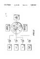
- FIG. 5illustrates a processing apparatus for carrying out the invention
- FIGS. 6-1 through 6-3illustrate, in cross-section, process steps in accordance with the invention for fabricating an EEPROM device.
- the process of the present inventionprovides a multi-layered dielectric material having a precisely tailored nitrogen concentration profile therein.
- the processfurther provides high nitrogen concentrations in regions of the dielectric material which are adjacent to electrically conductive bodies.
- Q bdcharge-to-breakdown
- oxynitride layer 14is formed in a thermally-controlled reactor. Initially, native oxide is removed from the surface 12 of substrate 10. Then, substrate 10 is heated to a temperature of about 900° to 1500° C., and nitrous oxide (N 2 O) is introduced into the reactor. In the reactor, a chemical reaction is carried out to form oxynitride layer 14 having a thickness of about 30 angstroms.
- the N 2 O reactionproduces a peak nitrogen concentration in oxynitride layer 14, which is narrowly defined in the central portion of the oxynitride layer. While not wishing to be bound by any particular theory of the invention, the inventors believe that the primary reaction species is nitric oxide (NO), which represents 4 to 10 atomic % of the initial quantity of N 2 O introduced into the reactor. However, the nitrogen bearing species, which reacts with silicon to form the oxynitride layer can also be N 2 O or NO 2 .
- SiO 2silicon dioxide layer
- SiO 2 layer 14oxygen is introduced into the reactor, and the oxygen is diffused through oxynitride layer 14 to substrate surface 12. The oxygen atoms react with silicon in substrate 10 to form SiO 2 layer 16. As SiO 2 layer 16 grows, substrate surface 12 recedes into substrate 10 as silicon atoms at the surface react with oxygen to form SiO 2 .
- oxynitride layer 14overlies SiO 2 layer 16, rather than substrate surface 12. Thus, silicon dioxide layer 16 lies intermediate to substrate 10 and oxynitride layer 14.
- SiO 2 layer 16is grown to a thickness of about 35 to 45 angstroms, and most preferably, to a thickness of 40 angstroms.
- the oxidation processis preferably carried out at a temperature of about 925° to 1150° C., and most preferably at about 950° C.
- very little of the oxygen diffusing through oxynitride layer 14reacts with the constituents of oxynitride layer 14.
- the majority of the oxygen species diffusing through oxynitride layer 14react with silicon to form SiO 2 . This is because, the reaction rate constant for the reaction of silicon with oxygen is substantially greater than the corresponding rate constant for the reaction of oxygen with the components of oxynitride layer 14.
- a second oxynitride layer 18is formed at substrate surface 12 below SiO 2 layer 16.
- substrate 10is again placed in a thermally-controlled reactor, and N 2 O is provided and NO is diffused through first oxynitride layer 14, and SiO 2 layer 16.
- the reaction gas moleculesdiffuse through the layers overlying substrate 10 to react with the silicon at substrate surface 12.
- the reaction rate constant for the reaction of NO with siliconis substantially greater than the corresponding reaction rate constant for the reaction between NO and SiO 2 .
- the NOdiffuses through both first oxynitride layer 14 and SiO 2 layer 16 without substantially reacting with the constituents of either layer.
- the kinetically favored reactionthen occurs between NO and the silicon atoms at substrate surface 12.
- the reaction between NO and siliconforms second oxynitride layer 18.
- the diffused speciesis believed to be NO, it is within the scope of the invention that another nitrogen-bearing species, such as N 2 O or NO 2 , can be diffused to form second oxynitride layer 18.
- First and second oxynitride layers 14 and 18, and SiO 2 layer 16comprise a composite dielectric layer 19.
- Composite dielectric layer 19is precisely constructed to contain regions of nitrogen accumulation at the interface between dielectric layer 19 and substrate 10 as well as the upper surface of dielectric layer 19.
- An important aspect of the present inventionincludes the ability of dielectric layer 19 to maintain high Q bd values over an extended period of time. The regions of nitrogen accumulation in composite dielectric layer 19 prevent the formation of electron trapping sites near the interfaces of dielectric layer 19. As will subsequently be described, the durability of dielectric layer 19 makes dielectric layer 19 especially useful as a tunnel gate dielectric material for an EEPROM device.
- FIG. 4illustrates, graphically, the nitrogen concentration distribution within the two oxynitride layers, and the intermediate SiO 2 layer.
- the topmost layer, oxynitride layer 14,is characterized by a large nitrogen concentration peak within the oxynitride layer. The peak concentration is displaced toward the upper surface of the oxynitride layer. A second nitrogen concentration peak occurs at the interface between second oxynitride layer 18 and the substrate.
- the stability of the Si-N bondsprevents the spreading of the nitrogen in first oxynitride layer 14 during the subsequent thermal processes used to form SiO 2 layer 16, and second oxynitride layer 18.
- the stability of the Si-N bondsalso accounts for the high nitrogen concentration observed at the interface between the substrate and second oxynitride layer 18.
- Processing apparatus 20includes gas supplies 22, 24, 26, and 28.
- the gas suppliesprovide source gases to process housing 30.
- Process housing 30contains processing chambers 32, 34, 36, and 38.
- a main mass flow controller 40selectively distributes gases which are input from the various gas supply sources to the various process chambers in housing 30.
- the flow of each source gasis regulated by independent mass flow controllers 42, 44, 46, and 48.
- the processing pressure within each of the process chambersis independently controlled by pressure controller 50, and the processing temperature in each chamber is independently controlled by temperature controller 52.
- an RF power supply 53provides RF power to selected chambers for plasma etching processes.
- the multi-chambered configuration of processing apparatus 20permits independent processing steps to be carried out in each of the individual processing chambers without subjecting the substrate work pieces to room-ambient conditions between processing steps.
- Substrate transfer meansare provided in processing apparatus 20 for the transfer of work pieces between the processing chambers, and to and from process housing 30.
- the processing steps illustrated in FIGS. 1-3can, for example, be carried out in processing apparatus 20 in the following manner.
- the processbegins with the transfer of substrate 10 to process chamber 32.
- cleaning gasis introduced from gas supply 28 through mass flow controller 48 and master valve 40.
- Substrate surface 12is processed in chamber 32 to remove all native oxide materials overlying substrate surface 12. This is accomplished, preferably, by introducing hydrogen fluorine gas (HF) into chamber 32, and reacting the HF with native oxide on substrate surface 12.
- HFhydrogen fluorine gas
- the surface cleaning reactioncan be performed by a plasma reaction in which the HF gas is energized in an RF field.
- N 2 Ois introduced from gas supply 24 through mass flow controller 44 and master valve 40.
- the temperature in chamber 34is controlled by temperature controller 52 within a range of preferably 900° to 1150° C., and most preferably, at 950° C.
- oxygenis introduced into chamber 34 from gas supply 26 through mass flow controller 46 and master valve 40, and SiO 2 layer 16 is grown on substrate surface 12.
- N 2 Ois again supplied from gas supply 24, and second oxynitride layer 18 is formed on substrate surface 12.
- the processcan be performed in separate processing chamber in processing apparatus 20.
- substrate 10is transferred to processing chamber 36.
- oxygenis introduced from gas supply 26 through mass flow controller 46 and master valve 40, and SiO 2 layer 16 is grown on substrate surface 12.
- substrate 10is transferred to processing chamber 38.
- N 2 Ois supplied from gas supply 24, and second oxynitride layer 18 is formed on substrate surface 12.
- process apparatus 20may also be formed in process apparatus 20, and additional cleaning steps can also be carried out.
- An important advantage of performing the processing steps in a processing apparatus such as apparatus 20,is achieved by excluding room-ambient atmosphere from substrate 20 between the various stages of processing.
- Each processing chamber in apparatus 20, as well as the transfer means,are constantly purged by an inert carrier gas supplied from gas supply 22. The presence of the inert carrier gas throughout apparatus 20, prevents native oxide materials from growing on any exposed surface of substrate 10 during the sequential processing steps.
- processing stepshave been described with respect to a preferred embodiment, which can be carried out in an apparatus such as apparatus 20, different methods can be used to form the composite dielectric layer of the invention.
- conventional, independent reactorscan be used to perform each step independently.
- precleaning processing stepsare necessary to ensure removal of native oxides prior to the formation of the oxynitride layers and the SiO 2 layer.
- FIGS. 6-1 through 6-3illustrate the application of the invention to the fabrication of an EEPROM device. Only those process steps necessary for explaining the invention are illustrated and described. The process, of course, may include other steps which are necessary for the fabrication of a complete device, but which do not involve the invention. To avoid confusion, these steps, which are conventionally used in semiconductor processing, have not been shown.
- FIG. 6-1illustrates, in cross-section, a portion of semiconductor substrate 10 having already undergone several process steps in accordance with the invention.
- an active region 54is defined by a field oxide region 56, which is formed in the surface of substrate 10.
- a gate dielectric layer 58overlies the surface of active region 54.
- Dielectric layer 58is preferably formed by thermal oxidation of substrate surface 12 using dry oxygen gas. The oxidation process is carried out at a temperature of about 925° to 975° C. and preferably at 950° C. During the oxidation process, the temperature is ramped-up to about 1,050° C. and an intermediate argon annealing step is performed.
- gate dielectric layer 58can be a dielectric material other than SiO 2 , such as chemical vapor deposited silicon nitride, silicon oxynitride, and the like.
- a photolithographic patternis formed on substrate 10, and ion implantation step is carried out to form tunnel region 63 in substrate 10.
- an etching processis performed to etch an opening 60 in a portion of gate dielectric layer 58 overlying tunnel region 63.
- the same photolithographic pattern used to define tunnel region 63can also be used to provide an etch mask for the formation of opening 60.
- other processing techniquescan be employed to form both tunnel region 63 and opening 60.
- separate photolithographic masking layerscan be used for the formation of opening 60 and tunnel region 63.
- Stacked-gate electrode 61includes a floating gate electrode 64, and inter-gate dielectric layer 66, and a control gate 68.
- stacked-gate electrode 61is formed by sequentially depositing a first polycrystalline silicon layer, a dielectric layer, and a second polycrystalline silicon layer. A photolithographic mask is defined on the second polysilicon layer and the polysilicon layers, and the intermediate gate dielectric layer are sequentially etched. Preferably, an anisotropic etching process is used to form stacked-gate electrode 61.
- inter-gate dielectric layer 66is formed by a combination of oxidation and silicon nitride deposition steps. These steps are carried out to fabricate an oxide-nitride-oxide (ONO) inter-gate dielectric layer.
- the polycrystalline silicon material used to form both floating gate electrode 64 and control gate electrode 68is doped with a conductivity determining dopant. The doping process is performed either during the deposition cycle, or immediately following deposition of the polycrystalline silicon.
- gate electrodes 64 and 68are doped with an N-type dopant, such as phosphorus, arsenic, antimony, and the like.
- an N-type dopantsuch as phosphorus, arsenic, antimony, and the like.
- composite dielectric layer 19functions as a tunnel gate dielectric material in an EEPROM device.
- the nitrogen accumulation characteristics of composite dielectric layer 19provide a region of high nitrogen concentration at the interface between floating gate electrodes 64 and composite dielectric layer 19. Additionally, a region of high nitrogen concentration also occurs at the interface between composite dielectric layer 19 and substrate surface 12.
- the presence of regions of high nitrogen concentration at the interfacesfunctions to enhance the durability of composite layer 19 as a tunnel dielectric material during successive program and erase cycles commonly used to store information in EEPROM devices.
- the nitrogen rich regions of composite dielectric layer 19reduce the formation of electron traps during Fowler-Nordheim tunneling at the programming and erasing stages.
- the presence of composite dielectric layer 19, formed in accordance with the inventionsubstantially increases the useful lifetime of a FETMOS EEPROM device.
- composite dielectric layer 19can be used as a tunneling dielectric material, the advantages obtained by the use of composite dielectric layer 19 can be applied to other devices.
- composite dielectric layer 19can be used as a capacitor dielectric in a thin-film capacitor.
- the high-reliability dielectric layercan be integrated into VLSI MOS transistors having lightly-doped drain structures.
- the dielectric layercan be used in P-type MOS (PMOS) devices. It is therefore intended to include within the invention all such variations and modifications as fall within the scope of the appended claims and equivalents thereof.
Landscapes
- Engineering & Computer Science (AREA)
- Condensed Matter Physics & Semiconductors (AREA)
- Crystallography & Structural Chemistry (AREA)
- General Chemical & Material Sciences (AREA)
- Physics & Mathematics (AREA)
- Chemical Kinetics & Catalysis (AREA)
- Chemical & Material Sciences (AREA)
- General Physics & Mathematics (AREA)
- Manufacturing & Machinery (AREA)
- Computer Hardware Design (AREA)
- Microelectronics & Electronic Packaging (AREA)
- Power Engineering (AREA)
- Formation Of Insulating Films (AREA)
Abstract
Description
Claims (16)
Priority Applications (2)
| Application Number | Priority Date | Filing Date | Title |
|---|---|---|---|
| US08/071,885US5407870A (en) | 1993-06-07 | 1993-06-07 | Process for fabricating a semiconductor device having a high reliability dielectric material |
| US08/186,957US5464792A (en) | 1993-06-07 | 1994-01-27 | Process to incorporate nitrogen at an interface of a dielectric layer in a semiconductor device |
Applications Claiming Priority (1)
| Application Number | Priority Date | Filing Date | Title |
|---|---|---|---|
| US08/071,885US5407870A (en) | 1993-06-07 | 1993-06-07 | Process for fabricating a semiconductor device having a high reliability dielectric material |
Related Child Applications (1)
| Application Number | Title | Priority Date | Filing Date |
|---|---|---|---|
| US08/186,957Continuation-In-PartUS5464792A (en) | 1993-06-07 | 1994-01-27 | Process to incorporate nitrogen at an interface of a dielectric layer in a semiconductor device |
Publications (1)
| Publication Number | Publication Date |
|---|---|
| US5407870Atrue US5407870A (en) | 1995-04-18 |
Family
ID=22104226
Family Applications (1)
| Application Number | Title | Priority Date | Filing Date |
|---|---|---|---|
| US08/071,885Expired - LifetimeUS5407870A (en) | 1993-06-07 | 1993-06-07 | Process for fabricating a semiconductor device having a high reliability dielectric material |
Country Status (1)
| Country | Link |
|---|---|
| US (1) | US5407870A (en) |
Cited By (64)
| Publication number | Priority date | Publication date | Assignee | Title |
|---|---|---|---|---|
| US5460992A (en)* | 1994-05-25 | 1995-10-24 | Nec Corporation | Fabricating non-volatile memory device having a multi-layered gate electrode |
| US5478765A (en)* | 1994-05-04 | 1995-12-26 | Regents Of The University Of Texas System | Method of making an ultra thin dielectric for electronic devices |
| US5541436A (en)* | 1994-01-07 | 1996-07-30 | The Regents Of The University Of Texas System | MOS transistor having improved oxynitride dielectric |
| US5552332A (en)* | 1995-06-02 | 1996-09-03 | Motorola, Inc. | Process for fabricating a MOSFET device having reduced reverse short channel effects |
| US5629221A (en)* | 1995-11-24 | 1997-05-13 | National Science Council Of Republic Of China | Process for suppressing boron penetration in BF2 + -implanted P+ -poly-Si gate using inductively-coupled nitrogen plasma |
| US5674788A (en)* | 1995-06-06 | 1997-10-07 | Advanced Micro Devices, Inc. | Method of forming high pressure silicon oxynitride gate dielectrics |
| US5712177A (en)* | 1994-08-01 | 1998-01-27 | Motorola, Inc. | Method for forming a reverse dielectric stack |
| US5714399A (en)* | 1994-12-14 | 1998-02-03 | Kabushiki Kaisha Toshiba | Semiconductor device having insulation film whose breakdown voltage is improved and its manufacturing method |
| US5714788A (en)* | 1995-12-27 | 1998-02-03 | Chartered Semiconductor Manufacturing, Pte Ltd. | Dual ion implantation process for gate oxide improvement |
| US5726087A (en)* | 1992-04-30 | 1998-03-10 | Motorola, Inc. | Method of formation of semiconductor gate dielectric |
| WO1998027580A1 (en)* | 1996-12-03 | 1998-06-25 | Scott Specialty Gases, Inc. | Process for forming ultrathin oxynitride layers and thin layer devices containing ultrathin oxynitride layers |
| US5821172A (en)* | 1997-01-06 | 1998-10-13 | Advanced Micro Devices, Inc. | Oxynitride GTE dielectrics using NH3 gas |
| US5837585A (en)* | 1996-07-23 | 1998-11-17 | Vanguard International Semiconductor Corporation | Method of fabricating flash memory cell |
| US5861651A (en)* | 1997-02-28 | 1999-01-19 | Lucent Technologies Inc. | Field effect devices and capacitors with improved thin film dielectrics and method for making same |
| US5866474A (en)* | 1997-07-17 | 1999-02-02 | United Microelectronics Corp. | Method for manufacturing gate oxide layers |
| US5880040A (en)* | 1996-04-15 | 1999-03-09 | Macronix International Co., Ltd. | Gate dielectric based on oxynitride grown in N2 O and annealed in NO |
| US5907183A (en)* | 1994-09-29 | 1999-05-25 | Nkk Corporation | Non-volatile semiconductor memory device |
| US5939763A (en)* | 1996-09-05 | 1999-08-17 | Advanced Micro Devices, Inc. | Ultrathin oxynitride structure and process for VLSI applications |
| US5960302A (en)* | 1996-12-31 | 1999-09-28 | Lucent Technologies, Inc. | Method of making a dielectric for an integrated circuit |
| US5972804A (en)* | 1997-08-05 | 1999-10-26 | Motorola, Inc. | Process for forming a semiconductor device |
| US5998270A (en)* | 1997-05-15 | 1999-12-07 | Advanced Micro Devices | Formation of oxynitride and polysilicon layers in a single reaction chamber |
| US6010935A (en)* | 1997-08-21 | 2000-01-04 | Micron Technology, Inc. | Self aligned contacts |
| US6020260A (en)* | 1997-06-25 | 2000-02-01 | Advanced Micro Devices, Inc. | Method of fabricating a semiconductor device having nitrogen-bearing gate electrode |
| US6037639A (en)* | 1997-06-09 | 2000-03-14 | Micron Technology, Inc. | Fabrication of integrated devices using nitrogen implantation |
| FR2783530A1 (en)* | 1998-09-21 | 2000-03-24 | Commissariat Energie Atomique | Silicon substrate preparation for insulating thin film formation, especially DRAM or EPROM gate oxide formation, comprises relatively low temperature treatment in a low pressure nitric oxide-based atmosphere |
| US6124620A (en)* | 1998-05-14 | 2000-09-26 | Advanced Micro Devices, Inc. | Incorporating barrier atoms into a gate dielectric using gas cluster ion beam implantation |
| US6140218A (en)* | 1999-06-10 | 2000-10-31 | Taiwan Semiconductor Manufacturing Company | Method for fabricating a T-shaped hard mask/conductor profile to improve self-aligned contact isolation |
| US6143598A (en)* | 1999-02-08 | 2000-11-07 | Chartered Semiconductor Manufacturing Ltd. | Method of fabrication of low leakage capacitor |
| US6187633B1 (en) | 1998-10-09 | 2001-02-13 | Chartered Semiconductor Manufacturing, Ltd. | Method of manufacturing a gate structure for a semiconductor memory device with improved breakdown voltage and leakage rate |
| US6197701B1 (en)* | 1998-10-23 | 2001-03-06 | Taiwan Semiconductor Manufacturing Company | Lightly nitridation surface for preparing thin-gate oxides |
| US6207587B1 (en) | 1997-06-24 | 2001-03-27 | Micron Technology, Inc. | Method for forming a dielectric |
| US6238985B1 (en)* | 1997-09-06 | 2001-05-29 | Lg Semicon Co., Ltd. | Semiconductor device and method for fabricating the same |
| US6242362B1 (en) | 1999-08-04 | 2001-06-05 | Taiwan Semiconductor Manufacturing Company | Etch process for fabricating a vertical hard mask/conductive pattern profile to improve T-shaped profile for a silicon oxynitride hard mask |
| US6245616B1 (en)* | 1999-01-06 | 2001-06-12 | International Business Machines Corporation | Method of forming oxynitride gate dielectric |
| US6248628B1 (en)* | 1999-10-25 | 2001-06-19 | Advanced Micro Devices | Method of fabricating an ONO dielectric by nitridation for MNOS memory cells |
| US6261976B1 (en) | 1999-03-18 | 2001-07-17 | Chartered Semiconductor Manufacturing Ltd. | Method of forming low pressure silicon oxynitride dielectrics having high reliability |
| US6274442B1 (en)* | 1998-07-15 | 2001-08-14 | Advanced Micro Devices, Inc. | Transistor having a nitrogen incorporated epitaxially grown gate dielectric and method of making same |
| US6297173B1 (en) | 1997-08-05 | 2001-10-02 | Motorola, Inc. | Process for forming a semiconductor device |
| US6348380B1 (en) | 2000-08-25 | 2002-02-19 | Micron Technology, Inc. | Use of dilute steam ambient for improvement of flash devices |
| US6350707B1 (en)* | 1999-09-03 | 2002-02-26 | United Microelectronics Corp. | Method of fabricating capacitor dielectric |
| US6355579B1 (en)* | 1999-02-22 | 2002-03-12 | Hyundai Electronics Industries Co., Ltd. | Method for forming gate oxide film in semiconductor device |
| US6373114B1 (en) | 1998-10-23 | 2002-04-16 | Micron Technology, Inc. | Barrier in gate stack for improved gate dielectric integrity |
| US6380056B1 (en) | 1998-10-23 | 2002-04-30 | Taiwan Semiconductor Manufacturing Company | Lightly nitridation surface for preparing thin-gate oxides |
| US6383861B1 (en) | 1999-02-18 | 2002-05-07 | Micron Technology, Inc. | Method of fabricating a dual gate dielectric |
| US6407008B1 (en)* | 2000-05-05 | 2002-06-18 | Integrated Device Technology, Inc. | Method of forming an oxide layer |
| US6433383B1 (en)* | 1999-07-20 | 2002-08-13 | Advanced Micro Devices, Inc. | Methods and arrangements for forming a single interpoly dielectric layer in a semiconductor device |
| US6458714B1 (en) | 2000-11-22 | 2002-10-01 | Micron Technology, Inc. | Method of selective oxidation in semiconductor manufacture |
| US6511876B2 (en)* | 2001-06-25 | 2003-01-28 | International Business Machines Corporation | High mobility FETS using A1203 as a gate oxide |
| US6583054B2 (en) | 1999-02-22 | 2003-06-24 | Hyundai Microelectronics Co., Ltd. | Method for forming conductive line in semiconductor device |
| US6642156B2 (en)* | 2001-08-01 | 2003-11-04 | International Business Machines Corporation | Method for forming heavy nitrogen-doped ultra thin oxynitride gate dielectrics |
| US6642095B2 (en)* | 2000-09-29 | 2003-11-04 | Hyundai Electronics Industries Co., Ltd. | Methods of fabricating semiconductor devices with barrier layers |
| US20030232507A1 (en)* | 2002-06-12 | 2003-12-18 | Macronix International Co., Ltd. | Method for fabricating a semiconductor device having an ONO film |
| US20040021170A1 (en)* | 1999-03-24 | 2004-02-05 | Caywood John M. | Method and apparatus for injecting charge onto the floating gate of a nonvolatile memory cell |
| US6721605B2 (en)* | 1999-09-10 | 2004-04-13 | Applied Materials, Inc. | Multi-computer chamber control system, method and medium |
| US6750157B1 (en)* | 2000-10-12 | 2004-06-15 | Advanced Micro Devices, Inc. | Nonvolatile memory cell with a nitridated oxide layer |
| US20040232499A1 (en)* | 2002-10-29 | 2004-11-25 | Hynix Semiconductor Inc. | Transistor in semiconductor devices and method of fabricating the same |
| US6890842B2 (en)* | 1996-01-31 | 2005-05-10 | Micron Technology, Inc. | Method of forming a thin film transistor |
| US20050263835A1 (en)* | 1999-11-05 | 2005-12-01 | Semiconductor Energy Laboratory Co., Ltd. | Semiconductor device, and method of fabricating the same |
| KR100611388B1 (en)* | 1999-12-30 | 2006-08-11 | 주식회사 하이닉스반도체 | Flash memory devices |
| US20070090493A1 (en)* | 2005-10-11 | 2007-04-26 | Promos Technologies Inc. | Fabrication of nitrogen containing regions on silicon containing regions in integrated circuits, and integrated circuits obtained thereby |
| US20070238313A1 (en)* | 2006-03-30 | 2007-10-11 | Tokyo Electron Limited | Method for replacing a nitrous oxide based oxidation process with a nitric oxide based oxidation process for substrate processing |
| US20070298622A1 (en)* | 2004-11-05 | 2007-12-27 | Hitachi Kokusai Electric Inc, | Producing Method of Semiconductor Device |
| US20100062595A1 (en)* | 2008-09-05 | 2010-03-11 | Juwan Lim | Nonvolatile memory device and method of forming the same |
| US9331184B2 (en) | 2013-06-11 | 2016-05-03 | United Microelectronics Corp. | Sonos device and method for fabricating the same |
Citations (7)
| Publication number | Priority date | Publication date | Assignee | Title |
|---|---|---|---|---|
| JPS60189972A (en)* | 1984-03-12 | 1985-09-27 | Hitachi Ltd | Semiconductor device and its manufacturing method |
| JPS62122222A (en)* | 1985-11-22 | 1987-06-03 | Hitachi Ltd | semiconductor equipment |
| US5198392A (en)* | 1989-11-20 | 1993-03-30 | Oki Electric Industry Co., Ltd. | Method of forming a nitrided silicon dioxide (SiOx Ny) film |
| US5225361A (en)* | 1990-03-08 | 1993-07-06 | Matshshita Electronics Coropration | Non-volatile semiconductor memory device and a method for fabricating the same |
| US5254506A (en)* | 1988-12-20 | 1993-10-19 | Matsushita Electric Industrial Co., Ltd. | Method for the production of silicon oxynitride film where the nitrogen concentration at the wafer-oxynitride interface is 8 atomic precent or less |
| US5258333A (en)* | 1992-08-18 | 1993-11-02 | Intel Corporation | Composite dielectric for a semiconductor device and method of fabrication |
| US5278087A (en)* | 1990-01-22 | 1994-01-11 | Silicon Storage Technology, Inc. | Method of making a single transistor non-volatile electrically alterable semiconductor memory device with a re-crystallized floating gate |
- 1993
- 1993-06-07USUS08/071,885patent/US5407870A/ennot_activeExpired - Lifetime
Patent Citations (7)
| Publication number | Priority date | Publication date | Assignee | Title |
|---|---|---|---|---|
| JPS60189972A (en)* | 1984-03-12 | 1985-09-27 | Hitachi Ltd | Semiconductor device and its manufacturing method |
| JPS62122222A (en)* | 1985-11-22 | 1987-06-03 | Hitachi Ltd | semiconductor equipment |
| US5254506A (en)* | 1988-12-20 | 1993-10-19 | Matsushita Electric Industrial Co., Ltd. | Method for the production of silicon oxynitride film where the nitrogen concentration at the wafer-oxynitride interface is 8 atomic precent or less |
| US5198392A (en)* | 1989-11-20 | 1993-03-30 | Oki Electric Industry Co., Ltd. | Method of forming a nitrided silicon dioxide (SiOx Ny) film |
| US5278087A (en)* | 1990-01-22 | 1994-01-11 | Silicon Storage Technology, Inc. | Method of making a single transistor non-volatile electrically alterable semiconductor memory device with a re-crystallized floating gate |
| US5225361A (en)* | 1990-03-08 | 1993-07-06 | Matshshita Electronics Coropration | Non-volatile semiconductor memory device and a method for fabricating the same |
| US5258333A (en)* | 1992-08-18 | 1993-11-02 | Intel Corporation | Composite dielectric for a semiconductor device and method of fabrication |
Non-Patent Citations (16)
| Title |
|---|
| Ahn, et al., "Furnace Nitridation of Thermal SiO2 in Pure N2O Ambient for ULSI MOS Applications," IEEE Electron Device Letters, vol. 13, No. 2, pp. 117-119 (Feb. 1992). |
| Ahn, et al., Furnace Nitridation of Thermal SiO2 in Pure N2O Ambient for ULSI MOS Applications, IEEE Electron Device Letters, vol. 13, No. 2, pp. 117 119 (Feb. 1992).* |
| Anonymous (R1788), "Under-grown multiple dielectric-layer semiconductor device," Research Disclosure 18756, Derwent Publications, Nov., 1979. |
| Anonymous (R1788), Under grown multiple dielectric layer semiconductor device, Research Disclosure 18756, Derwent Publications, Nov., 1979.* |
| Fukuda, et al., "High-Performance Scaled Flash-Type EEPROMs with Heavily Oxynitrided Tunnel Oxide Films," IEDM, pp. 465-468 (1992). |
| Fukuda, et al., High Performance Scaled Flash Type EEPROMs with Heavily Oxynitrided Tunnel Oxide Films, IEDM, pp. 465 468 (1992).* |
| Haddad, et al., "Improvement of Thin-Gate Oxide Integrity Using Through-Silicon-Gate Nitrogen Ion Implantation," IEEE Electron Dev. Letters, vol. EDL-8 No. 2, pp. 58-60 (1987). |
| Haddad, et al., Improvement of Thin Gate Oxide Integrity Using Through Silicon Gate Nitrogen Ion Implantation, IEEE Electron Dev. Letters, vol. EDL 8 No. 2, pp. 58 60 (1987).* |
| Lo, et al., "Improved Hot-Carrier Immunity in CMOS Analog Device with N2O-Nitrided Gate Oxides" IEEE Electron Dev. Letters, vol. 13, NO. 11, pp. 457-459 (Sep. 8, 1992). |
| Lo, et al., "Improved Performance and Reliability of MOSFETs with Ultrathin Gate Oxides . . . ," Symposium on VLSI Technology, pp. 43-44 (1991). |
| Lo, et al., Improved Hot Carrier Immunity in CMOS Analog Device with N2O Nitrided Gate Oxides IEEE Electron Dev. Letters, vol. 13, NO. 11, pp. 457 459 (Sep. 8, 1992).* |
| Lo, et al., Improved Performance and Reliability of MOSFETs with Ultrathin Gate Oxides . . . , Symposium on VLSI Technology, pp. 43 44 (1991).* |
| Ohnishi, et al., "Ultrathin Oxide/Nitride/Oxide/Nitride Multilayer Films for Mbit DRAM Capacitors," Solid State Devices & Materials Ext. Abstracts of '92 Int. Conf., pp. 67-69 (1992). |
| Ohnishi, et al., Ultrathin Oxide/Nitride/Oxide/Nitride Multilayer Films for Mbit DRAM Capacitors, Solid State Devices & Materials Ext. Abstracts of 92 Int. Conf., pp. 67 69 (1992).* |
| Yoon, et al., "MOS Characteristics of NH3-Nitrided N20-Grown Oxides," IEEE Electron Dev. Letters, (14), No. 4, pp. 179-181 (Apr. 1993). |
| Yoon, et al., MOS Characteristics of NH3 Nitrided N20 Grown Oxides, IEEE Electron Dev. Letters, (14), No. 4, pp. 179 181 (Apr. 1993).* |
Cited By (113)
| Publication number | Priority date | Publication date | Assignee | Title |
|---|---|---|---|---|
| US5726087A (en)* | 1992-04-30 | 1998-03-10 | Motorola, Inc. | Method of formation of semiconductor gate dielectric |
| US5541436A (en)* | 1994-01-07 | 1996-07-30 | The Regents Of The University Of Texas System | MOS transistor having improved oxynitride dielectric |
| US5478765A (en)* | 1994-05-04 | 1995-12-26 | Regents Of The University Of Texas System | Method of making an ultra thin dielectric for electronic devices |
| US5460992A (en)* | 1994-05-25 | 1995-10-24 | Nec Corporation | Fabricating non-volatile memory device having a multi-layered gate electrode |
| US5712177A (en)* | 1994-08-01 | 1998-01-27 | Motorola, Inc. | Method for forming a reverse dielectric stack |
| US5907183A (en)* | 1994-09-29 | 1999-05-25 | Nkk Corporation | Non-volatile semiconductor memory device |
| US5714399A (en)* | 1994-12-14 | 1998-02-03 | Kabushiki Kaisha Toshiba | Semiconductor device having insulation film whose breakdown voltage is improved and its manufacturing method |
| US6163050A (en)* | 1994-12-14 | 2000-12-19 | Kabushiki Kaisha Toshiba | Semiconductor device having insulation film whose breakdown voltage is improved and its manufacturing method |
| US5552332A (en)* | 1995-06-02 | 1996-09-03 | Motorola, Inc. | Process for fabricating a MOSFET device having reduced reverse short channel effects |
| US5674788A (en)* | 1995-06-06 | 1997-10-07 | Advanced Micro Devices, Inc. | Method of forming high pressure silicon oxynitride gate dielectrics |
| DE19680529B4 (en)* | 1995-06-06 | 2010-11-04 | Advanced Micro Devices Inc., Austin | A method of making high pressure silicon oxynitride (oxynitride) gate dielectrics for metal oxide semiconductor (MOS) devices with polycrystalline P + silicon (polysilicon) gate electrodes |
| US5629221A (en)* | 1995-11-24 | 1997-05-13 | National Science Council Of Republic Of China | Process for suppressing boron penetration in BF2 + -implanted P+ -poly-Si gate using inductively-coupled nitrogen plasma |
| US5714788A (en)* | 1995-12-27 | 1998-02-03 | Chartered Semiconductor Manufacturing, Pte Ltd. | Dual ion implantation process for gate oxide improvement |
| US20050156240A1 (en)* | 1996-01-31 | 2005-07-21 | Sandhu Gurtej S. | Thin film transistors and semiconductor constructions |
| US7566907B2 (en) | 1996-01-31 | 2009-07-28 | Micron Technology, Inc. | Thin film transistors and semiconductor constructions |
| US7825414B2 (en) | 1996-01-31 | 2010-11-02 | Micron Technology, Inc. | Method of forming a thin film transistor |
| US20090302322A1 (en)* | 1996-01-31 | 2009-12-10 | Micron Technology, Inc. | Method of Forming a Thin Film Transistor |
| US20090047776A1 (en)* | 1996-01-31 | 2009-02-19 | Micron Technology, Inc. | Method of Forming a Thin Film Transistor |
| US7452760B2 (en) | 1996-01-31 | 2008-11-18 | Micron Technology, Inc. | Thin film transistors and semiconductor constructions |
| US6890842B2 (en)* | 1996-01-31 | 2005-05-10 | Micron Technology, Inc. | Method of forming a thin film transistor |
| US20080237601A1 (en)* | 1996-01-31 | 2008-10-02 | Sandhu Gurtej S | Transistors and semiconductor constructions |
| US20070102705A1 (en)* | 1996-01-31 | 2007-05-10 | Sandhu Gurtej S | Thin film transistors and semiconductor constructions |
| US7385222B2 (en) | 1996-01-31 | 2008-06-10 | Micron Technology, Inc. | Thin film transistors and semiconductor constructions |
| US5880040A (en)* | 1996-04-15 | 1999-03-09 | Macronix International Co., Ltd. | Gate dielectric based on oxynitride grown in N2 O and annealed in NO |
| US5837585A (en)* | 1996-07-23 | 1998-11-17 | Vanguard International Semiconductor Corporation | Method of fabricating flash memory cell |
| US5939763A (en)* | 1996-09-05 | 1999-08-17 | Advanced Micro Devices, Inc. | Ultrathin oxynitride structure and process for VLSI applications |
| US6245689B1 (en)* | 1996-09-05 | 2001-06-12 | Advanced Micro Devices, Inc. | Process for reliable ultrathin oxynitride formation |
| WO1998027580A1 (en)* | 1996-12-03 | 1998-06-25 | Scott Specialty Gases, Inc. | Process for forming ultrathin oxynitride layers and thin layer devices containing ultrathin oxynitride layers |
| US5960302A (en)* | 1996-12-31 | 1999-09-28 | Lucent Technologies, Inc. | Method of making a dielectric for an integrated circuit |
| US5821172A (en)* | 1997-01-06 | 1998-10-13 | Advanced Micro Devices, Inc. | Oxynitride GTE dielectrics using NH3 gas |
| US5861651A (en)* | 1997-02-28 | 1999-01-19 | Lucent Technologies Inc. | Field effect devices and capacitors with improved thin film dielectrics and method for making same |
| US5998270A (en)* | 1997-05-15 | 1999-12-07 | Advanced Micro Devices | Formation of oxynitride and polysilicon layers in a single reaction chamber |
| US7071067B1 (en) | 1997-06-09 | 2006-07-04 | Micron Technology, Inc. | Fabrication of integrated devices using nitrogen implantation |
| US6037639A (en)* | 1997-06-09 | 2000-03-14 | Micron Technology, Inc. | Fabrication of integrated devices using nitrogen implantation |
| US6432841B1 (en) | 1997-06-24 | 2002-08-13 | Micron Technology, Inc. | Method for forming a dielectric |
| US6207587B1 (en) | 1997-06-24 | 2001-03-27 | Micron Technology, Inc. | Method for forming a dielectric |
| US6020260A (en)* | 1997-06-25 | 2000-02-01 | Advanced Micro Devices, Inc. | Method of fabricating a semiconductor device having nitrogen-bearing gate electrode |
| US5866474A (en)* | 1997-07-17 | 1999-02-02 | United Microelectronics Corp. | Method for manufacturing gate oxide layers |
| US5972804A (en)* | 1997-08-05 | 1999-10-26 | Motorola, Inc. | Process for forming a semiconductor device |
| US6297173B1 (en) | 1997-08-05 | 2001-10-02 | Motorola, Inc. | Process for forming a semiconductor device |
| US6010935A (en)* | 1997-08-21 | 2000-01-04 | Micron Technology, Inc. | Self aligned contacts |
| US6057581A (en)* | 1997-08-21 | 2000-05-02 | Micron Technology, Inc. | Self-aligned contacts |
| US6238985B1 (en)* | 1997-09-06 | 2001-05-29 | Lg Semicon Co., Ltd. | Semiconductor device and method for fabricating the same |
| US6455380B2 (en) | 1997-09-06 | 2002-09-24 | Lg Semicon Co., Ltd | Semiconductor device and method for fabricating the same |
| US6124620A (en)* | 1998-05-14 | 2000-09-26 | Advanced Micro Devices, Inc. | Incorporating barrier atoms into a gate dielectric using gas cluster ion beam implantation |
| US6274442B1 (en)* | 1998-07-15 | 2001-08-14 | Advanced Micro Devices, Inc. | Transistor having a nitrogen incorporated epitaxially grown gate dielectric and method of making same |
| US6551698B1 (en) | 1998-09-21 | 2003-04-22 | Commissariat A L'energie Atomique | Method for treating a silicon substrate, by nitriding, to form a thin insulating layer |
| WO2000017412A1 (en)* | 1998-09-21 | 2000-03-30 | Commissariat A L'energie Atomique | Method for treating, by nitriding, a silicon substrate for forming a thin insulating layer |
| FR2783530A1 (en)* | 1998-09-21 | 2000-03-24 | Commissariat Energie Atomique | Silicon substrate preparation for insulating thin film formation, especially DRAM or EPROM gate oxide formation, comprises relatively low temperature treatment in a low pressure nitric oxide-based atmosphere |
| SG84527A1 (en)* | 1998-10-09 | 2001-11-20 | Chartered Semiconductor Mfg | Method for manufacturing a gate structure for a semiconductor memory device with improved breakdown voltage and leakage rate |
| US6187633B1 (en) | 1998-10-09 | 2001-02-13 | Chartered Semiconductor Manufacturing, Ltd. | Method of manufacturing a gate structure for a semiconductor memory device with improved breakdown voltage and leakage rate |
| US6380056B1 (en) | 1998-10-23 | 2002-04-30 | Taiwan Semiconductor Manufacturing Company | Lightly nitridation surface for preparing thin-gate oxides |
| US6770571B2 (en) | 1998-10-23 | 2004-08-03 | Micron Technology, Inc. | Barrier in gate stack for improved gate dielectric integrity |
| US6197701B1 (en)* | 1998-10-23 | 2001-03-06 | Taiwan Semiconductor Manufacturing Company | Lightly nitridation surface for preparing thin-gate oxides |
| US20050017312A1 (en)* | 1998-10-23 | 2005-01-27 | Nanseng Jeng | Barrier in gate stack for improved gate dielectric integrity |
| US6373114B1 (en) | 1998-10-23 | 2002-04-16 | Micron Technology, Inc. | Barrier in gate stack for improved gate dielectric integrity |
| US6930363B2 (en) | 1998-10-23 | 2005-08-16 | Micron Technology, Inc. | Barrier in gate stack for improved gate dielectric integrity |
| US6562730B2 (en) | 1998-10-23 | 2003-05-13 | Micron Technology, Inc. | Barrier in gate stack for improved gate dielectric integrity |
| US20030139061A1 (en)* | 1998-10-23 | 2003-07-24 | Nanseng Jeng | Barrier in gate stack for improved gate dielectric integrity |
| US6245616B1 (en)* | 1999-01-06 | 2001-06-12 | International Business Machines Corporation | Method of forming oxynitride gate dielectric |
| US6143598A (en)* | 1999-02-08 | 2000-11-07 | Chartered Semiconductor Manufacturing Ltd. | Method of fabrication of low leakage capacitor |
| SG81287A1 (en)* | 1999-02-08 | 2001-06-19 | Chartered Semiconductor Mfg | Method of fabrication of low leakage capacitor |
| US20040113229A1 (en)* | 1999-02-18 | 2004-06-17 | Fernando Gonzalez | Dual gate dielectric construction |
| US6653675B2 (en) | 1999-02-18 | 2003-11-25 | Micron Technology, Inc. | Dual gate dielectric construction |
| US6946713B2 (en) | 1999-02-18 | 2005-09-20 | Micron Technology, Inc. | Multiple thickness gate dielectric layers |
| US6383861B1 (en) | 1999-02-18 | 2002-05-07 | Micron Technology, Inc. | Method of fabricating a dual gate dielectric |
| US6583054B2 (en) | 1999-02-22 | 2003-06-24 | Hyundai Microelectronics Co., Ltd. | Method for forming conductive line in semiconductor device |
| US6355579B1 (en)* | 1999-02-22 | 2002-03-12 | Hyundai Electronics Industries Co., Ltd. | Method for forming gate oxide film in semiconductor device |
| SG84533A1 (en)* | 1999-03-18 | 2001-11-20 | Chartered Semiconductor Mfg | Method of forming low pressure silicon oxynitride dielectrics having high reliability |
| US6261976B1 (en) | 1999-03-18 | 2001-07-17 | Chartered Semiconductor Manufacturing Ltd. | Method of forming low pressure silicon oxynitride dielectrics having high reliability |
| US20040021170A1 (en)* | 1999-03-24 | 2004-02-05 | Caywood John M. | Method and apparatus for injecting charge onto the floating gate of a nonvolatile memory cell |
| US6140218A (en)* | 1999-06-10 | 2000-10-31 | Taiwan Semiconductor Manufacturing Company | Method for fabricating a T-shaped hard mask/conductor profile to improve self-aligned contact isolation |
| US6433383B1 (en)* | 1999-07-20 | 2002-08-13 | Advanced Micro Devices, Inc. | Methods and arrangements for forming a single interpoly dielectric layer in a semiconductor device |
| US6242362B1 (en) | 1999-08-04 | 2001-06-05 | Taiwan Semiconductor Manufacturing Company | Etch process for fabricating a vertical hard mask/conductive pattern profile to improve T-shaped profile for a silicon oxynitride hard mask |
| US6350707B1 (en)* | 1999-09-03 | 2002-02-26 | United Microelectronics Corp. | Method of fabricating capacitor dielectric |
| US6721605B2 (en)* | 1999-09-10 | 2004-04-13 | Applied Materials, Inc. | Multi-computer chamber control system, method and medium |
| US6248628B1 (en)* | 1999-10-25 | 2001-06-19 | Advanced Micro Devices | Method of fabricating an ONO dielectric by nitridation for MNOS memory cells |
| US20070029626A1 (en)* | 1999-11-05 | 2007-02-08 | Semiconductor Energy Laboratory Co., Ltd. | Semiconductor device, and method of fabricating the same |
| US7372114B2 (en) | 1999-11-05 | 2008-05-13 | Semiconductor Energy Laboratory Co., Ltd. | Semiconductor device, and method of fabricating the same |
| US20050263835A1 (en)* | 1999-11-05 | 2005-12-01 | Semiconductor Energy Laboratory Co., Ltd. | Semiconductor device, and method of fabricating the same |
| US7166899B2 (en)* | 1999-11-05 | 2007-01-23 | Semiconductor Energy Laboratory Co., Ltd. | Semiconductor device, and method of fabricating the same |
| KR100611388B1 (en)* | 1999-12-30 | 2006-08-11 | 주식회사 하이닉스반도체 | Flash memory devices |
| US6407008B1 (en)* | 2000-05-05 | 2002-06-18 | Integrated Device Technology, Inc. | Method of forming an oxide layer |
| US20100032746A1 (en)* | 2000-08-25 | 2010-02-11 | Micron Technology, Inc. | Use of dilute steam ambient for improvement of flash devices |
| US6348380B1 (en) | 2000-08-25 | 2002-02-19 | Micron Technology, Inc. | Use of dilute steam ambient for improvement of flash devices |
| US20020117709A1 (en)* | 2000-08-25 | 2002-08-29 | Weimer Ronald A. | Use of dilute steam ambient for improvement of flash devices |
| US6949789B2 (en) | 2000-08-25 | 2005-09-27 | Micron Technology, Inc. | Use of dilute steam ambient for improvement of flash devices |
| US7989870B2 (en) | 2000-08-25 | 2011-08-02 | Micron Technology, Inc. | Use of dilute steam ambient for improvement of flash devices |
| US7585725B2 (en) | 2000-08-25 | 2009-09-08 | Micron Technology, Inc. | Use of dilute steam ambient for improvement of flash devices |
| US20060011969A1 (en)* | 2000-08-25 | 2006-01-19 | Weimer Ronald A | Use of dilute steam ambient for improvement of flash devices |
| US8294192B2 (en) | 2000-08-25 | 2012-10-23 | Micron Technology, Inc. | Use of dilute steam ambient for improvement of flash devices |
| US20090004794A1 (en)* | 2000-08-25 | 2009-01-01 | Micron Technology, Inc. | Use of dilute steam ambient for improvement of flash devices |
| US7432546B2 (en) | 2000-08-25 | 2008-10-07 | Micron Technology, Inc. | Apparatus having a memory device with floating gate layer grain boundaries with oxidized portions |
| US6642095B2 (en)* | 2000-09-29 | 2003-11-04 | Hyundai Electronics Industries Co., Ltd. | Methods of fabricating semiconductor devices with barrier layers |
| US6750157B1 (en)* | 2000-10-12 | 2004-06-15 | Advanced Micro Devices, Inc. | Nonvolatile memory cell with a nitridated oxide layer |
| US6458714B1 (en) | 2000-11-22 | 2002-10-01 | Micron Technology, Inc. | Method of selective oxidation in semiconductor manufacture |
| US6511876B2 (en)* | 2001-06-25 | 2003-01-28 | International Business Machines Corporation | High mobility FETS using A1203 as a gate oxide |
| US6642156B2 (en)* | 2001-08-01 | 2003-11-04 | International Business Machines Corporation | Method for forming heavy nitrogen-doped ultra thin oxynitride gate dielectrics |
| US20030232507A1 (en)* | 2002-06-12 | 2003-12-18 | Macronix International Co., Ltd. | Method for fabricating a semiconductor device having an ONO film |
| US7535067B2 (en)* | 2002-10-29 | 2009-05-19 | Magnachip Semiconductor, Ltd. | Transistor in semiconductor devices and method of fabricating the same |
| US20040232499A1 (en)* | 2002-10-29 | 2004-11-25 | Hynix Semiconductor Inc. | Transistor in semiconductor devices and method of fabricating the same |
| US7795156B2 (en)* | 2004-11-05 | 2010-09-14 | Hitachi Kokusai Electric Inc. | Producing method of semiconductor device |
| US20070298622A1 (en)* | 2004-11-05 | 2007-12-27 | Hitachi Kokusai Electric Inc, | Producing Method of Semiconductor Device |
| US20070138579A1 (en)* | 2005-10-11 | 2007-06-21 | Zhong Dong | Fabrication of nitrogen containing regions on silicon containing regions in integrated circuits, and integrated circuits obtained thereby |
| US20070090493A1 (en)* | 2005-10-11 | 2007-04-26 | Promos Technologies Inc. | Fabrication of nitrogen containing regions on silicon containing regions in integrated circuits, and integrated circuits obtained thereby |
| US7635655B2 (en) | 2006-03-30 | 2009-12-22 | Tokyo Electron Limited | Method for replacing a nitrous oxide based oxidation process with a nitric oxide based oxidation process for substrate processing |
| US20070238313A1 (en)* | 2006-03-30 | 2007-10-11 | Tokyo Electron Limited | Method for replacing a nitrous oxide based oxidation process with a nitric oxide based oxidation process for substrate processing |
| US20100062595A1 (en)* | 2008-09-05 | 2010-03-11 | Juwan Lim | Nonvolatile memory device and method of forming the same |
| US8420482B2 (en)* | 2008-09-05 | 2013-04-16 | Samsung Electronics Co., Ltd. | Nonvolatile memory device and method of forming the same |
| KR101410429B1 (en)* | 2008-09-05 | 2014-07-03 | 삼성전자주식회사 | Non-volatile memory device and methods of forming the same |
| USRE46389E1 (en)* | 2008-09-05 | 2017-05-02 | Samsung Electronics Co., Ltd. | Nonvolatile memory device and method of forming the same |
| US9331184B2 (en) | 2013-06-11 | 2016-05-03 | United Microelectronics Corp. | Sonos device and method for fabricating the same |
| US9508734B2 (en) | 2013-06-11 | 2016-11-29 | United Microelectronics Corp. | Sonos device |
Similar Documents
| Publication | Publication Date | Title |
|---|---|---|
| US5407870A (en) | Process for fabricating a semiconductor device having a high reliability dielectric material | |
| US5464792A (en) | Process to incorporate nitrogen at an interface of a dielectric layer in a semiconductor device | |
| US11721733B2 (en) | Memory transistor with multiple charge storing layers and a high work function gate electrode | |
| US9306025B2 (en) | Memory transistor with multiple charge storing layers and a high work function gate electrode | |
| US7075139B2 (en) | Method of manufacturing semiconductor device | |
| US5861347A (en) | Method for forming a high voltage gate dielectric for use in integrated circuit | |
| US6818558B1 (en) | Method of manufacturing a dielectric layer for a silicon-oxide-nitride-oxide-silicon (SONOS) type devices | |
| TWI436455B (en) | Semiconductor-Oxide-Nitride-Oxide-Semiconductor (SONOS) Oxide-Nitride-Oxide (ONO) Stacking Scaling | |
| US6100559A (en) | Multipurpose graded silicon oxynitride cap layer | |
| US7001810B2 (en) | Floating gate nitridation | |
| US20070269972A1 (en) | Method of manufacturing a semiconductor device | |
| US4011576A (en) | Nonvolatile semiconductor memory devices | |
| US20230081072A1 (en) | Method of Integrating SONOS into HKMG Flow | |
| US5208174A (en) | Method for manufacturing a nonvolatile semiconductor memory device | |
| JP2002217317A (en) | Non-volatile semiconductor storage device and its manufacturing method | |
| US6433383B1 (en) | Methods and arrangements for forming a single interpoly dielectric layer in a semiconductor device | |
| US4735919A (en) | Method of making a floating gate memory cell | |
| US20040053468A1 (en) | Method for forming a protective buffer layer for high temperature oxide processing | |
| US6329247B1 (en) | Nonvolatile semiconductor memory device and manufacturing method thereof | |
| US6162684A (en) | Ammonia annealed and wet oxidized LPCVD oxide to replace ono films for high integrated flash memory devices | |
| US5925908A (en) | Integrated circuit including a non-volatile memory device and a semiconductor device | |
| US8222094B2 (en) | Method for manufacturing an EEPROM cell | |
| US6828201B1 (en) | Method of manufacturing a top insulating layer for a sonos-type device | |
| US4683640A (en) | Method of making a floating gate memory cell | |
| US20060094257A1 (en) | Low thermal budget dielectric stack for SONOS nonvolatile memories |
Legal Events
| Date | Code | Title | Description |
|---|---|---|---|
| AS | Assignment | Owner name:MOTOROLA, INC., ILLINOIS Free format text:ASSIGNMENT OF ASSIGNORS INTEREST;ASSIGNORS:OKADA, YOSHIO;TOBIN, PHILIP J.;REEL/FRAME:006572/0239 Effective date:19930528 | |
| STPP | Information on status: patent application and granting procedure in general | Free format text:APPLICATION UNDERGOING PREEXAM PROCESSING | |
| FPAY | Fee payment | Year of fee payment:4 | |
| FPAY | Fee payment | Year of fee payment:8 | |
| AS | Assignment | Owner name:FREESCALE SEMICONDUCTOR, INC., TEXAS Free format text:ASSIGNMENT OF ASSIGNORS INTEREST;ASSIGNOR:MOTOROLA, INC.;REEL/FRAME:015698/0657 Effective date:20040404 Owner name:FREESCALE SEMICONDUCTOR, INC.,TEXAS Free format text:ASSIGNMENT OF ASSIGNORS INTEREST;ASSIGNOR:MOTOROLA, INC.;REEL/FRAME:015698/0657 Effective date:20040404 | |
| FPAY | Fee payment | Year of fee payment:12 | |
| AS | Assignment | Owner name:CITIBANK, N.A. AS COLLATERAL AGENT, NEW YORK Free format text:SECURITY AGREEMENT;ASSIGNORS:FREESCALE SEMICONDUCTOR, INC.;FREESCALE ACQUISITION CORPORATION;FREESCALE ACQUISITION HOLDINGS CORP.;AND OTHERS;REEL/FRAME:018855/0129 Effective date:20061201 Owner name:CITIBANK, N.A. AS COLLATERAL AGENT,NEW YORK Free format text:SECURITY AGREEMENT;ASSIGNORS:FREESCALE SEMICONDUCTOR, INC.;FREESCALE ACQUISITION CORPORATION;FREESCALE ACQUISITION HOLDINGS CORP.;AND OTHERS;REEL/FRAME:018855/0129 Effective date:20061201 | |
| AS | Assignment | Owner name:CITIBANK, N.A., AS COLLATERAL AGENT,NEW YORK Free format text:SECURITY AGREEMENT;ASSIGNOR:FREESCALE SEMICONDUCTOR, INC.;REEL/FRAME:024397/0001 Effective date:20100413 Owner name:CITIBANK, N.A., AS COLLATERAL AGENT, NEW YORK Free format text:SECURITY AGREEMENT;ASSIGNOR:FREESCALE SEMICONDUCTOR, INC.;REEL/FRAME:024397/0001 Effective date:20100413 | |
| AS | Assignment | Owner name:ZOZO MANAGEMENT, LLC, DELAWARE Free format text:ASSIGNMENT OF ASSIGNORS INTEREST;ASSIGNOR:FREESCALE SEMICONDUCTOR, INC.;REEL/FRAME:034034/0236 Effective date:20120814 | |
| AS | Assignment | Owner name:APPLE INC., CALIFORNIA Free format text:ASSIGNMENT OF ASSIGNORS INTEREST;ASSIGNOR:ZOZO MANAGEMENT, LLC;REEL/FRAME:034732/0019 Effective date:20141219 | |
| AS | Assignment | Owner name:FREESCALE SEMICONDUCTOR, INC., TEXAS Free format text:PATENT RELEASE;ASSIGNOR:CITIBANK, N.A., AS COLLATERAL AGENT;REEL/FRAME:037354/0225 Effective date:20151207 Owner name:FREESCALE SEMICONDUCTOR, INC., TEXAS Free format text:PATENT RELEASE;ASSIGNOR:CITIBANK, N.A., AS COLLATERAL AGENT;REEL/FRAME:037356/0553 Effective date:20151207 Owner name:FREESCALE SEMICONDUCTOR, INC., TEXAS Free format text:PATENT RELEASE;ASSIGNOR:CITIBANK, N.A., AS COLLATERAL AGENT;REEL/FRAME:037356/0143 Effective date:20151207 |