US5406434A - Thin film head with contoured pole face edges for undershoot reduction - Google Patents
Thin film head with contoured pole face edges for undershoot reductionDownload PDFInfo
- Publication number
- US5406434A US5406434AUS08/263,009US26300994AUS5406434AUS 5406434 AUS5406434 AUS 5406434AUS 26300994 AUS26300994 AUS 26300994AUS 5406434 AUS5406434 AUS 5406434A
- Authority
- US
- United States
- Prior art keywords
- pole tip
- magnetic
- gap region
- magnetic flux
- outer edge
- Prior art date
- Legal status (The legal status is an assumption and is not a legal conclusion. Google has not performed a legal analysis and makes no representation as to the accuracy of the status listed.)
- Expired - Lifetime
Links
Images


Classifications
- G—PHYSICS
- G11—INFORMATION STORAGE
- G11B—INFORMATION STORAGE BASED ON RELATIVE MOVEMENT BETWEEN RECORD CARRIER AND TRANSDUCER
- G11B5/00—Recording by magnetisation or demagnetisation of a record carrier; Reproducing by magnetic means; Record carriers therefor
- G11B5/127—Structure or manufacture of heads, e.g. inductive
- G11B5/1278—Structure or manufacture of heads, e.g. inductive specially adapted for magnetisations perpendicular to the surface of the record carrier
- G—PHYSICS
- G11—INFORMATION STORAGE
- G11B—INFORMATION STORAGE BASED ON RELATIVE MOVEMENT BETWEEN RECORD CARRIER AND TRANSDUCER
- G11B5/00—Recording by magnetisation or demagnetisation of a record carrier; Reproducing by magnetic means; Record carriers therefor
- G11B5/127—Structure or manufacture of heads, e.g. inductive
- G11B5/31—Structure or manufacture of heads, e.g. inductive using thin films
- G11B5/3109—Details
- G11B5/3116—Shaping of layers, poles or gaps for improving the form of the electrical signal transduced, e.g. for shielding, contour effect, equalizing, side flux fringing, cross talk reduction between heads or between heads and information tracks
- G—PHYSICS
- G11—INFORMATION STORAGE
- G11B—INFORMATION STORAGE BASED ON RELATIVE MOVEMENT BETWEEN RECORD CARRIER AND TRANSDUCER
- G11B5/00—Recording by magnetisation or demagnetisation of a record carrier; Reproducing by magnetic means; Record carriers therefor
- G11B5/127—Structure or manufacture of heads, e.g. inductive
- G11B5/31—Structure or manufacture of heads, e.g. inductive using thin films
- G11B5/3163—Fabrication methods or processes specially adapted for a particular head structure, e.g. using base layers for electroplating, using functional layers for masking, using energy or particle beams for shaping the structure or modifying the properties of the basic layers
- Y—GENERAL TAGGING OF NEW TECHNOLOGICAL DEVELOPMENTS; GENERAL TAGGING OF CROSS-SECTIONAL TECHNOLOGIES SPANNING OVER SEVERAL SECTIONS OF THE IPC; TECHNICAL SUBJECTS COVERED BY FORMER USPC CROSS-REFERENCE ART COLLECTIONS [XRACs] AND DIGESTS
- Y10—TECHNICAL SUBJECTS COVERED BY FORMER USPC
- Y10T—TECHNICAL SUBJECTS COVERED BY FORMER US CLASSIFICATION
- Y10T29/00—Metal working
- Y10T29/49—Method of mechanical manufacture
- Y10T29/49002—Electrical device making
- Y10T29/4902—Electromagnet, transformer or inductor
- Y10T29/49021—Magnetic recording reproducing transducer [e.g., tape head, core, etc.]
- Y10T29/49032—Fabricating head structure or component thereof
- Y10T29/49036—Fabricating head structure or component thereof including measuring or testing
- Y10T29/49043—Depositing magnetic layer or coating
- Y10T29/49044—Plural magnetic deposition layers
Definitions
- the present inventionrelates to production of thin film magnetic heads.
- the inventionrelates to aligning the upper and lower pole tips in a thin film magnetic head using a sacrificial layer yielding a contoured pole face which provides reduced undershoot in a readback signal.
- Thin film magnetic read/write headsare used for magnetically reading and writing information upon a magnetic storage medium such as a magnetic disc or a magnetic tape. It is highly desirable to provide a high density of information storage on the magnetic storage medium.
- Magnetic headsare now fabricated in a manner similar to that used for semiconductor integrated circuits in the electronic industry.
- many thin film magnetic headsare deposited across the surface of a wafer (or substrate). After the layers are deposited, the wafer is "diced” or sliced into many individual thin film heads, each carried by a portion of the wafer so that an upper pole tip, a lower pole tip, and a gap are exposed. The pole tips and the gap (and the portion of the substrate which underlies them) are then lapped in a direction generally inward, toward the center of the thin film head, to achieve the desired dimensions.
- This lapping processis a grinding process in which the exposed portion of the top and bottom pole tips and the gap are applied to an abrasive, such as a diamond slurry. Electrical contacts are connected to conductive coils.
- the completed headis attached to a carrying fixture for use in reading and writing data on a magnetic storage medium such as a computer disc.
- the exposed upper and lower pole tipsare positioned near a moving magnetic storage medium.
- the changing magnetic flux of the moving storage mediumimpresses a changing magnetic flux upon upper and lower pole tips.
- the magnetic fluxis carried through the pole tips and yoke core around the conductor coil.
- the changing magnetic fluxinduces an electrical voltage across the conductor coil which may be detected with electrical detection circuitry.
- the electrical voltageis representative of the changing magnetic flux produced by the moving magnetic storage medium.
- an electrical currentis caused to flow in the conductor coil.
- This electric currentinduces a magnetic field in top and bottom magnetic poles and causes a magnetic field across the gap between the upper and lower pole tips.
- a fringe fieldextends in the vicinity beyond the boundary of the pole tips and into the nearby magnetic storage medium. This fringe field may be used to impress magnetic fields upon the storage medium and magnetically write information.
- Magnetic pole tipstypically have a pole thickness in the range of about one micrometer to about five micrometers depending upon design criteria, i.e. a thicker pole for better overwriting efficiency and a thinner pole for increased resolution capability during the readback operation.
- the structureis then aligned using a material removal process ("milling") such as ion milling or reactive ion milling in which high energy ions bombard the pole tip region to remove the excess material (top pole, bottom pole and gap material) that extends beyond the edges of the mask layer.
- millingsuch as ion milling or reactive ion milling in which high energy ions bombard the pole tip region to remove the excess material (top pole, bottom pole and gap material) that extends beyond the edges of the mask layer.
- the mask layerprotects only a portion of the top pole, bottom pole and gap so that the width of the completed pole tips is approximately the same as the width of the mask layer.
- the noted alignment techniquesuffers from a number of drawbacks.
- the mask layeris difficult to remove from the pole tip structure after the milling process. To ensure adequate protection of the pole tips during milling, the mask must be very thick to withstand the milling process. A thick mask, however, decreases the ability to control the shape of the pole tips. Furthermore, if the remaining mask material is stripped away following milling, the delicate structure of the thin film head may be damaged. If, on the other hand, the mask layer is made thinner to improve process control and facilitate removal of the mask following ion milling, the risk of damaging the pole tip structure during milling is increased.
- the thin film headDuring readback of magnetically stored information, the thin film head provides an electrical output signal which is representative of both the relative strength of the magnetization in the media, and the magnetic field pattern of the read head. It is highly desirable to provide the highest level of information storage density possible for a given magnetic storage system. Unfortunately, increased storage density leads to a lower signal-to-noise ratio for the sensed signal from a given disk.
- the readback signalcomprises a series of superimposed symbols whose existence and location are used to represent digital information.
- Cost effective detectors presently in useare confused by leading and trailing undershoots in the isolated readback pulses just as easily as they are confused by noise. This is because for an arbitrary recorded pattern, the undershoot readback waveform from one recorded transition can interfere with the main pulse of another transition and result in one of the above signal recovery errors.
- the undershootsreduce the maximum recording density which may be achieved in a magnetic storage system. Undershoot occurs due to discontinuities in the magnetic readback flux path characteristic of the finite pole lengths of the thin film recording head. Rather than trying to compensate for the undershoots in the data signal using sophisticated electronic decoding methods, it would be highly desirable and a significant contribution to the art to provide a thin film magnetic head which minimizes the leading and trailing undershoots in the isolated readback pulse.
- the present inventionprovides closely aligned pole tips which yield reduced undershoots in isolated readback pulses in a thin film magnetic transducer. This may be used to yield increased data storage densities.
- the top poleis aligned with the bottom pole using dams made with the aid of a sacrificial layer.
- the damsare formed by depositing an encapsulation layer over a sacrificial layer.
- the sacrificial layeris deposited in substantial self alignment with the bottom pole.
- the sacrificial layeris removed through any suitable alternative. These alternatives include lapping, milling, selective chemical etching, lift-off, and removing through thermal or physical shock.
- the cavityis filled with magnetic material to form the top pole. During this process, a nonmagnetic gap is formed between the top pole and the bottom pole.
- photoresist damsare deposited upon a substrate which carries the thin film magnetic head.
- a bottom poleis deposited between the photoresist dams.
- a sacrificial layeris deposited between the same photoresist dams upon the bottom pole.
- the sacrificial layeris a layer of copper.
- the photoresist damsare removed and the pole tip region is coated with an encapsulation layer, typically of Al 2 O 3 .
- the encapsulation layer which covers the sacrificial layeris removed along with the sacrificial layer. Following this removal, the encapsulation layer forms dams on either side of the bottom pole. The dams extend above the sides of the bottom pole.
- a gap layeris deposited over the bottom pole layer.
- the gap layercomprises Al 2 O 3 .
- Additional photoresist damsare deposited upon the gap Al 2 O 3 layer and are generally in alignment with the bottom pole.
- a top pole layeris deposited upon the gap Al 2 O 3 layer. The top pole is aligned with the bottom pole by the dams formed by the encapsulation layer.
- the encapsulation layer which overlies the bottom pole and covers the sacrificial layermay be removed using a number of techniques.
- the encapsulation layercan be removed using a lapping process. In the lapping process, the pole tip region is lapped so that the encapsulation layer is removed and the sacrificial layer is exposed.
- the sacrificial layeris selectively etched which leaves dams extended above either side of the bottom pole.
- the overlying encapsulation layercan also be removed using a lift-off process.
- the encapsulation layeris deposited by a sputtering technique in which a sufficiently negative electrical bias potential and sufficiently high gas pressure are used to reduce deposition of the encapsulation layer at the corners of sacrificial layer. Following deposition of the encapsulation layer, a small amount of ion milling or chemical etching will expose the edges of sacrificial layer under the encapsulation layer.
- the overlying encapsulation layeris removed through lift-off using a selective chemical etch for the sacrificial layer. Again, dams are formed from the encapsulation layer which are aligned with the lower pole.
- the top polemay be deposited as described above.
- the encapsulation layercan be removed by depositing photoresist dams on the encapsulation layer which leave a portion of the encapsulation layer exposed. A selective chemical etch is applied which etches the exposed portion of the encapsulation layer. The sacrificial layer and the photoresist dams are removed. Again, dams are formed from the encapsulation layer which are aligned with the lower pole. The top pole may be deposited as described above.
- the encapsulation layercan also be removed by physical or thermal shock. If the encapsulation layer is sputtered upon the surface with a zero electrical bias potential, it will adhere poorly to the sacrificial layer. The structure can then be subjected to physical or thermal shocks which cause the overlying encapsulation layer to break free of the sacrificial layer.
- the sacrificial layeris selectively chemically etched and the top pole is deposited between the dams formed by the encapsulation layer and in alignment with the lower pole.
- the present inventionprovides dams which are aligned with the bottom pole which can be used to deposit the top pole.
- the damsare formed in an encapsulation layer with a sacrificial layer.
- the encapsulation layer which overlies the sacrificial layeris removed using three alternative processes.
- Al 2 O 3provides an excellent encapsulation layer material because Al 2 O 3 is nonmagnetic and residual Al 2 O 3 will not degrade thin film head operation.
- the present inventionprovides reduced undershoot in an isolated readback pulse in a readback signal. This is achieved due to the contour of the outside pole face edges of the pole tips.
- the contour of the outside pole tips of the present inventionare significantly different from the contour at the gap, which is a straight line.
- the undershoot response from the outside pole face edgeis concentrated along the portion of the contour which is furthest from the gap edge.
- the present inventionprovides a contour in which this concentration takes place at the edges of the gap, or slightly outside the edges of the gap. This region does not contain well defined transitions which are parallel to the gap surface, and is usually considered to be an erased region.
- a pole face edgehas a significantly different contour if a cross-section of the pole tip has thickness variations which are greater than about the thickness of the magnetic flux gap region, especially if the thickest portion occurs at or outside of the gap edge, or forms a pinnacle which extends in a direction away from the gap.
- an edge contour of the pole tipsforms buck horns.
- FIG. 1shows a top view of a thin film magnetic read/write head.
- FIG. 2is a side cross sectional view of the thin film magnetic head of FIG. 1 taken along line 2--2.
- FIG. 3Ais a cross-sectional view of a substrate.
- FIG. 3Bis a cross-sectional view of the substrate of FIG. 3A including photoresist dams.
- FIG. 3Cis a cross-sectional view of a substrate including a lower pole piece.
- FIG. 3Dis a cross-sectional view of a substrate which includes a sacrificial layer.
- FIG. 3Eis a cross-sectional view of a substrate following removal of photoresist dams.
- FIG. 3Fis a cross-sectional view of a substrate following deposition of an Al 2 O 3 layer.
- FIG. 4Ais a cross-sectional view of a substrate following a lapping process.
- FIG. 4Bis cross-sectional view of a substrate following removal of a sacrificial layer.
- FIG. 4Cis cross-sectional view of a substrate following deposition of an Al 2 O 3 gap layer.
- FIG. 4Dis cross-sectional view following deposition of photoresist dams.
- FIG. 4Eis a cross-sectional view of a substrate following deposition of a top pole piece.
- FIG. 4Fis a cross-sectional view of FIG. 1 taken along line 4F--4F.
- FIG. 5Ais a cross-sectional view of a substrate which shows an encapsulation layer.
- FIG. 5Bis a cross-sectional view of a substrate including an encapsulation layer and a partially exposed sacrificial layer.
- FIG. 6Ais a cross-sectional view of a substrate which shows an encapsulation layer and photoresist dams.
- FIG. 6Bis a cross-sectional view of a substrate including photoresist dams and a partially exposed sacrificial layer.
- FIG. 7shows an isolated readback pulse for a prior art thin film magnetic head.
- FIG. 8shows an isolated readback pulse for a thin film magnetic head having a top pole tip made in accordance with the present invention.
- FIGS. 9A through 9Eshow steps in making a thin magnetic head having upper and lower pole tips made in accordance with the present invention which reduce undershoot in an isolated readback pulse.
- FIG. 10shows contoured pole tips having a contour in accordance with the present invention.
- FIG. 11shows contoured pole tips having a contour in accordance with the present invention.
- FIG. 12is a cross sectional view of a pole tip face of a probe head used for vertical magnetic record made in accordance with the present invention.
- FIGS. 1 and 2A multi-turn inductive thin film magnetic head 10 is shown schematically in FIGS. 1 and 2.
- FIG. 1is a top view of thin film head 10 and
- FIG. 2is a side cross sectional view.
- Thin film head 10includes top pole 12 and bottom pole 14.
- Top pole 12 and bottom pole 14form a magnetic thin film core and comprise a nickel-iron (NiFe) alloy. Photolithography is used to define the geometry of both top pole 12 and bottom pole 14 of the magnetic core.
- Conductive coils 16 and 18extend between top and bottom magnetic thin film poles 12 and 14 and are electrically insulated from magnetic core poles 12 and 14 by an insulating layer 20.
- Thin film head 10is deposited upon a nonmagnetic substrate 22 which comprises a ceramic composite compound, such as Al 2 O 3 -TiC. Typically an Al 2 O 3 base coat (not shown) separates the substrate of the bottom pole.
- FIGS. 3A-3Fshow the initial steps of pole tip alignment used in the present invention.
- FIG. 3Ais a cross-sectional view of ceramic substrate 22. Ceramic substrate 22 forms the base upon which thin film head 10 (shown in FIG. 2) is fabricated.
- FIG. 3Bis a cross-sectional view of substrate 22 including photoresist dams 30A and 30B.
- Photoresist dams 30A and 30Bare formed by depositing a layer of photoresist across the surface of substrate 22. A portion of the photoresist layer is exposed to ultraviolet radiation. A special chemical etch is applied which removes the portion of the photoresist which was exposed to the radiation.
- FIG. 3Cis a cross-sectional view of substrate 22 with photoresist dams 30A and 30B and a bottom pole 32.
- Bottom pole 32comprises NiFe.
- Bottom pole 32may comprise any magnetic material.
- Photoresist dams 30A and 30Bdefine the edges of bottom pole 32.
- FIG. 3Dis a cross-sectional view of substrate 22 which shows a sacrificial layer 34.
- Sacrificial layer 34is deposited upon bottom pole 32 between photoresist dams 30A and 30B.
- Photoresist dams 30A and 30Bdefine the edges of sacrificial layer 34.
- sacrificial layer 34comprises copper. As shown in FIG. 3D, because sacrificial layer 34 is deposited using photoresist dams 30A and 30B used to deposit bottom pole 32, sacrificial layer 34 is in substantial alignment with bottom pole 32.
- FIG. 3Eshows another step in the process of the present invention.
- photoresist dams 30A and 30Bhave been stripped away.
- Photoresist dams 30A and 30Bare stripped using a selective chemical etch which attacks only the photoresist dams 30A and 30B.
- the chemical etchleaves bottom pole 32 and sacrificial layer 34 substantially intact as shown in FIG. 3E.
- FIG. 3Fis a cross-sectional view of substrate 22 following deposition of an encapsulation layer 36.
- Encapsulation layer 36preferably comprises Al 2 O 3 .
- Encapsulation layer 36is deposited across the surface of substrate 22 and substantially encapsulates bottom pole 32 and sacrificial layer 34 as depicted in FIG. 3F.
- Encapsulation layer 36may be deposited using a sputtering technique. The electrical bias and gas pressure applied during the sputtering process changes characteristics of the encapsulation layer 36.
- sacrificial layer 34may be removed using a suitable procedure to leave the edges of encapsulation layer 36 substantially intact.
- Encapsulation layer 36forms two dams used in a subsequent deposition process. Between the two dams an upper pole is deposited which is in substantial alignment with the bottom pole.
- FIGS. 4A through 4Fshow the steps of one alternative process for removing the sacrificial layer through lapping and selective chemical etching.
- FIG. 4Aa cross-sectional view of substrate 22, encapsulation layer 36 has been lapped to expose a surface of sacrificial layer 34.
- the lapping processis a process in which a surface is applied to an abrasive which wears the surface down.
- encapsulation layer 36has been lapped to expose sacrificial layer 34 without substantially removing sacrificial layer 34.
- encapsulation layer 36forms two separate pieces, dam 36A and dam 36B.
- FIG. 4Bshows a cross-sectional view of substrate 22 following a selective chemical etch of sacrificial layer 34.
- sacrificial layer 34comprises copper
- a selective chemical etchwould be applied which attacks only copper and does not significantly alter lower pole 32 and dams 36A and 36B.
- FIG. 4Cis a cross-sectional view of substrate 22 including a gap layer 38.
- gap layer 38comprises Al 2 O 3 .
- this gap layer 38comprises the same material as dams 36A and 36B.
- Gap layer 38is a non-magnetic material which forms a gap between the two magnetic pole tips in the thin film head.
- FIG. 4Dis a cross-sectional view of substrate 22 including photoresist dams 40A and 40B.
- Photoresist dams 40A and 40Bare used in forming a top pole 42 (shown in FIG. 4E).
- the alignment of photoresist dams 40A and 40B with lower pole 32is not as critical as the alignment of dams 36A and 36B with lower pole 32.
- Photoresist dams 40A and 40Bare deposited using a layer of photoresist which is selectively exposed to activating radiation and then chemically etched.
- FIG. 4Eshows a cross-sectional view of substrate 22 including upper pole 42.
- Upper pole 42is deposited upon gap layer 38 and in substantial alignment with bottom pole 32.
- Dams 36A and 36Bprovide a close alignment between upper pole 42 and lower pole 32.
- the photoresist dams 40A and 40Balso contain the outer edges of upper pole 42.
- upper pole 42comprises NiFe.
- Upper pole 42is used to complete a magnetic flux circuit between upper pole 42 and lower pole 32 across gap layer 38.
- FIG. 4Fis a cross-sectional view of substrate 22 following removal of photoresist dams 40A and 40B.
- FIG. 4Fshows a substantially complete cross-sectional view of thin film head 10 shown in FIG. 1 taken along line 4F--4F.
- the structure of FIG. 4Fis encapsulated in a non-magnetic material such as Al 2 O 3 .
- Dams 36A and 36Bremain deposited upon substrate 22 after completion of the fabrication process.
- Upper pole 42rises up, away from the gap area, in regions 43A and 43B which reduce undershoot in isolated readback pulses in accordance with the present invention.
- Gap layer 38has a thickness 45.
- Regions 43A and 43Bare also referred to herein as "buck horns.” Buck horns 43A and 43B introduce a thickness variation 47 in upper pole 42 which is greater than about half of gap thickness 45, in accordance with the present invention.
- FIG. 5Ashows another alternative embodiment of forming dams with a sacrificial layer in accordance with the present invention.
- FIG. 5Ais a cross-sectional view of substrate 22.
- an encapsulation layer 44is deposited upon lower pole 32 and sacrificial layer 34.
- encapsulation layer 44comprises Al 2 O 3 , a non-magnetic material.
- Encapsulation layer 44is sputtered upon substrate 22 and sacrificial layer 34.
- an electrical bias potentialis applied which is sufficiently negative to form a incline in encapsulation layer 44 at corners 46A and 46B of sacrificial layer 34.
- electrical bias between the substrate and the sourceshould be between about -100 volts and about -160 volts, which is about 10% to 16% of the target voltage.
- Gas pressureshould be about 10 milliTorr to 20 milliTorr. These parameters depend upon characteristics of the deposition process.
- encapsulation layer 44is relatively thin near corners 46A and 46B of sacrificial layer 34.
- FIG. 5Bshows a cross-sectional view of substrate 22 in which corners 46A and 46B of sacrificial layer 34 are exposed through encapsulation layer 44 to create side portion 44A, side portion 44B and center portion 44C. Corners 46A and 46B of encapsulation layer 44 are exposed by slightly ion milling encapsulation layer 44 shown in FIG. 5A or by applying a mild chemical etch to encapsulation layer 44. Alternatively, the electrical bias applied during sputtering and the amount of material sputtered down may be adjusted so that corners 46A and 46B are not completely covered by encapsulation layer 44.
- a selective chemical etchcan be applied to sacrificial layer 34.
- sacrificial layer 34comprises copper
- a copper chemical etchcan be applied. This lifts off the portion 44C of encapsulation layer 44 which overlies sacrificial layer 34.
- the result and cross-sectional viewis similar to the cross-sectional view shown in FIG. 4B.
- Subsequent stepscan be followed to fabricate an upper pole 42 as shown FIGS. 4C through 4F.
- FIGS. 6A and 6Bshow another alternative embodiment of forming dams with a sacrificial layer in accordance with the present invention.
- FIG. 6Ashows a cross-sectional view of a substrate 22 in which lower pole 32 and sacrificial layer 34 is covered by an encapsulation layer 48.
- photoresist dams 50A and 50Bpartially cover encapsulation layer 48 and leave a portion of encapsulation layer 48 exposed.
- a selective chemical etchis applied to encapsulation layer 48 which selectively etches only the material of encapsulation layer 48.
- Photoresist dams 50A and 50Bare chemically stripped.
- Sacrificial layer 34is selectively etched. This leaves an encapsulation layer dam structure similar to that shown in FIG. 4B.
- the cavity formed between encapsulation layer dams 48A and 48Bmay be filled with a top pole piece as described above.
- the encapsulation layeris sputtered using an electrical bias of zero volts. Gas pressure should be about 20 to about 30 milliTorr. These parameters depend upon the sputtering mechanism. This causes the encapsulation layer to weakly adhere to the sacrificial layer.
- the portion of the encapsulation layer which overlies the sacrificial layermay be removed by subjecting the structure to physical or thermal shocks. The physical or thermal shocks cause the encapsulation layer to break free from the sacrificial layer and leave behind dams on either side of the lower pole.
- the sacrificial layercan be removed using a selective chemical etch as described above.
- FIG. 7is a graph of an isolated readback pulse 52 of a prior art magnetic head which includes undershoots 54 and 56. These undershoots are due to the change in the magnetic flux linking the head coils from the magnetic storage medium, as a magnetic transition in the media passes under each outside pole face edge.
- FIG. 8is a graph of an isolated readback pulse from a thin film magnetic head made in accordance with the present invention.
- the thin film magnetic head which generated isolated readback pulse 58has a top pole with regions 43A and 43B as shown in FIG. 4F.
- this shapesignificantly reduces undershoot, in this case the trailing undershoot, as shown in FIG. 8. Since only the shape of the top pole outside edge is changed and not the bottom pole outside edge, a leading undershoot 60 remains in isolated readback pulse 58. However, if the shape of a bottom pole outside edge were also changed in accordance with the present invention, the amplitude of undershoot 60 would also be significantly reduced.
- FIGS. 9A through 9Eshow steps used in fabricating thin film magnetic head pole tips in which both upper and lower pole tips have regions at or beyond the sides of the gap, which extend away from the gap, to reduce leading and trailing undershoots in the resulting isolated readback pulse, in accordance with the present invention.
- a non-magnetic substrate 62carries a coating of alumina (Al 2 O 3 ) base coat layer 64.
- a photoresist mask 66is deposited upon alumina base coat layer 64.
- Mask 66should have dimensions which are wide enough to leave a large enough base for a bottom pole to be deposited even if undercut occurs during a subsequent etching step.
- a chemical etchantis applied which attacks alumina base coat 64.
- alumina base coat 64can be etched down approximately three micrometer (3 ⁇ m) using a bath of 10% HF solution in deionized water. Alternatively, sputter etching with ion milling, or any physical etching process can be used. This forms a plateau 68 in alumina base coat 64. After forming plateau 68, photoresist mask 66 is removed. Next, masks 70A and 70B shown in FIG. 9C are deposited just beyond the edges of plateau 68. A first bottom pole layer 72 is plated between masks 70A and 70B. First bottom pole layer 72 includes buck horns 73A and 73B in accordance with the present invention. Masks 70A and 70B are then removed.
- photoresist masks 74A and 74Bare deposited on the first bottom pole layer 72 as shown in FIG. 9D.
- a second bottom pole layer 76is deposited between photoresist masks 74A and 74B.
- First bottom pole layer 72 and second bottom pole layer 76combine to form bottom pole 78.
- Bottom pole 78has a shape, relative to the gap, which is similar to the shape of upper pole 42 shown in FIG. 4F.
- an upper pole 80is deposited as shown in FIG. 9E.
- Upper pole 80can be deposited in a manner similar to that described above, such as that shown in FIGS. 4A through 4F.
- a gap region 85separates poles 78 and 80.
- Upper pole 80includes buck horns 81A and 81B in accordance with the present invention.
- the resulting pole structurehas an upper pole 80 and a lower pole 78 both of which have regions at the sides of the gap which extend away from the gap. This shape eliminates both leading and trailing undershoots. Additionally, upper pole tip 80 and lower pole tip 78 are in substantial alignment with each other. Lower pole tip 78 can be formed using any suitable physical process.
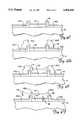
- FIGS. 10 and 11show a number of different pole tip contours in accordance with the present invention.
- an upper pole tip 82 and a lower pole tip 84have rounded contours along the edges which are far from a gap 86.
- FIG. 11shows an upper pole tip 94 and a lower pole tip 96 which provide a narrower region along the edge which protrudes farther from a gap 98.
- FIGS. 9E, 10, and 11all show various implementations of the present invention.
- the significant feature of pole tips made in accordance with the present inventionis that the contour along an outer edge of the pole tip is significantly different than the contour along the gap edge of the pole tip.
- pole tips in accordance with the present inventionhave thickness variations which are greater than about one half the thickness of a magnetic flux gap region.
- pole tip shapes in accordance with the present inventioncan be used in magnetic probe heads which are used for vertical recording on perpendicular magnetic media.
- FIG. 12shows a cross-section of a pole tip face 100 from a probe head which is used for vertical magnetic recording.
- Pole tip face 100includes a thick magnetic closure pole 102, with integral track edge fringing, shields 108A and 108B, top pole 104, and a thick gap 106.
- the flux pathis usually completed by a soft magnetic layer which is deposited beneath the high coercivity recording layer in the recording media.
- Shields 108A and 108Bare used to improve off-track characteristics of magnetic probe 100.
- Gap edge 110creates a leading undershoot in isolated readback pulses. However, if a gap edge shown by dashed line 112 is used in magnetic probe 100, undershoot is believed to be reduced in accordance with the present invention.
- Contouring gap edge 110 differently than the gap edge provided by upper pole tip 104is the equivalent to contouring the outside pole face edges differently than the gap for a longitudinal recording head as described above. Although a curved shape is shown for gap edge 112, other contoured shapes may be used for the gap edges in accordance with the present invention.
- gap edge contour 112should be significantly different than the contour of top pole 104.
- "significantly different”means that contour thickness 114 of gap edge contour 112 should be more than about one quarter of thickness 116 of top pole 104.
- the present inventionprovides a method of fabricating closely aligned pole tips in a thin film magnetic head.
- a top poleis aligned with a bottom pole using dams made with a sacrificial layer.
- the damsare formed by depositing an encapsulation layer over the sacrificial layer. When the sacrificial layer is removed, the encapsulation layer which overlies the sacrificial layer is removed. This provides two dams formed from the encapsulation layer on either side of the bottom pole. These dams are used to form the top pole in substantial alignment with the bottom pole.
- the present inventionreduces undershoot in isolated readback pulses by providing contoured edges in the pole tip face.
- the contouracts to attenuate and broaden the undershoot by either spreading the effective sensitivity of the pole face edge over a longer distance in a direction perpendicular to the gap, concentrating the sensitivity to undershoot at the erased zones at the sides of the gap, dispersing the sensitivity to undershoot in directions which differ greatly from the axis of magnetization in the media, or by a combination thereof.
- This techniquemay be used along outer pole tip edges in longitudinal recording heads, and along inner pole tip edges in vertical recording heads.
- the encapsulation layer and sacrificial layermay be formed using any suitable material such as a ceramic, a glass or Si, and the steps of forming dams with the encapsulation by removing the sacrificial layer may be through any suitable means.
- the sacrificial layermay comprise any suitable selectively etchable layer and the magnetic layers may comprise magnetic material other than NiFe.
- different pole tip edge contourscan be used to reduce undershoot in isolated readback pulses and pole tip shapes in accordance with the present invention can be made using any suitable technique.
Landscapes
- Engineering & Computer Science (AREA)
- Manufacturing & Machinery (AREA)
- Magnetic Heads (AREA)
Abstract
Description
Claims (7)
Priority Applications (1)
| Application Number | Priority Date | Filing Date | Title |
|---|---|---|---|
| US08/263,009US5406434A (en) | 1990-11-06 | 1994-06-20 | Thin film head with contoured pole face edges for undershoot reduction |
Applications Claiming Priority (5)
| Application Number | Priority Date | Filing Date | Title |
|---|---|---|---|
| US07/609,921US5084957A (en) | 1990-11-06 | 1990-11-06 | Method for aligning thin film head pole tips |
| US07/702,956US5137750A (en) | 1990-11-06 | 1991-05-20 | Method of making a thin film head with contoured pole face edges for undershoot reduction |
| US87987492A | 1992-05-19 | 1992-05-19 | |
| US5592293A | 1993-04-29 | 1993-04-29 | |
| US08/263,009US5406434A (en) | 1990-11-06 | 1994-06-20 | Thin film head with contoured pole face edges for undershoot reduction |
Related Parent Applications (1)
| Application Number | Title | Priority Date | Filing Date |
|---|---|---|---|
| US5592293AContinuation | 1990-11-06 | 1993-04-29 |
Publications (1)
| Publication Number | Publication Date |
|---|---|
| US5406434Atrue US5406434A (en) | 1995-04-11 |
Family
ID=27086155
Family Applications (2)
| Application Number | Title | Priority Date | Filing Date |
|---|---|---|---|
| US07/702,956Expired - LifetimeUS5137750A (en) | 1990-11-06 | 1991-05-20 | Method of making a thin film head with contoured pole face edges for undershoot reduction |
| US08/263,009Expired - LifetimeUS5406434A (en) | 1990-11-06 | 1994-06-20 | Thin film head with contoured pole face edges for undershoot reduction |
Family Applications Before (1)
| Application Number | Title | Priority Date | Filing Date |
|---|---|---|---|
| US07/702,956Expired - LifetimeUS5137750A (en) | 1990-11-06 | 1991-05-20 | Method of making a thin film head with contoured pole face edges for undershoot reduction |
Country Status (1)
| Country | Link |
|---|---|
| US (2) | US5137750A (en) |
Cited By (20)
| Publication number | Priority date | Publication date | Assignee | Title |
|---|---|---|---|---|
| EP0752699A1 (en)* | 1995-07-05 | 1997-01-08 | Read-Rite Corporation | Alignment of magnetic poles of thin film transducer |
| US5726841A (en)* | 1996-06-11 | 1998-03-10 | Read-Rite Corporation | Thin film magnetic head with trimmed pole tips etched by focused ion beam for undershoot reduction |
| US5761014A (en)* | 1995-06-30 | 1998-06-02 | Nec Corporation | Thin film magnetic head with magnetically insulating layer for suppressing undershoots |
| US5801909A (en)* | 1994-08-26 | 1998-09-01 | Aiwa Research And Development, Inc. | Thin film magnetic head including durable wear layer and non-magnetic gap structures |
| US5909346A (en)* | 1994-08-26 | 1999-06-01 | Aiwa Research & Development, Inc. | Thin magnetic film including multiple geometry gap structures on a common substrate |
| US5910871A (en)* | 1996-04-25 | 1999-06-08 | Hitachi, Ltd. | Magnetic head having track width specified by grooves formed with projection ion beam |
| US5940253A (en)* | 1996-12-30 | 1999-08-17 | Quantum Corporation | Laminated plated pole pieces for thin film magnetic transducers |
| US5978187A (en)* | 1994-11-14 | 1999-11-02 | Yamaha Corporation | Thin film magnetic head having a lower pole shaped to improve reproduction characteristics |
| US5991110A (en)* | 1994-01-25 | 1999-11-23 | Tdk Corporation | Thin film magnetic head and magnetic recording and reproducing apparatus |
| US6069015A (en)* | 1996-05-20 | 2000-05-30 | Aiwa Research And Development, Inc. | Method of fabricating thin film magnetic head including durable wear layer and non-magnetic gap structure |
| US6072672A (en)* | 1997-05-06 | 2000-06-06 | International Business Machines Corporation | Write head with notched P1 and minimum overmilled P1 and P2 |
| US6166879A (en)* | 1996-10-31 | 2000-12-26 | Aiwa Co., Ltd. | Thin film magnetic head with contoured surface |
| US6445536B1 (en)* | 1998-08-27 | 2002-09-03 | Read-Rite Corporation | Dielectric stencil-defined write head for MR, GMR, and spin valve high density recording heads |
| US6521335B1 (en) | 1998-05-07 | 2003-02-18 | Seagate Technology, Inc. | Method of fabricating a submicron narrow writer pole |
| US6785953B2 (en) | 2001-06-18 | 2004-09-07 | International Business Machines Corporation | Process of fabricating a write head with protection of a second pole tip thickness |
| US6788496B2 (en) | 2001-08-22 | 2004-09-07 | Seagate Technology Llc | Narrow top pole of a write element |
| US20050024781A1 (en)* | 2003-07-29 | 2005-02-03 | Seagate Technology Llc | Magnetoresistive sensor |
| US20060132971A1 (en)* | 2003-12-15 | 2006-06-22 | Seagate Technology Llc | Magnetic recording head with compact yoke |
| US7298587B2 (en) | 2002-08-05 | 2007-11-20 | Seagate Technology Llc | Rounded top pole |
| US20090117407A1 (en)* | 2007-11-02 | 2009-05-07 | Yi Zheng | Short flare definition by additive process for perpendicular head |
Families Citing this family (22)
| Publication number | Priority date | Publication date | Assignee | Title |
|---|---|---|---|---|
| US5479310A (en)* | 1991-03-20 | 1995-12-26 | Yamaha Corporation | Thin film magnetic head having a variable thickness magnetic layer |
| JPH04310608A (en)* | 1991-04-09 | 1992-11-02 | Matsushita Electric Ind Co Ltd | Manufacture of thin film magnetic head |
| US5687045A (en)* | 1991-09-20 | 1997-11-11 | Hitachi, Ltd. | Thin film magnetic head and production method thereof and magnetic disk drive equipped with this thin film magnetic head |
| JP2715808B2 (en)* | 1992-06-09 | 1998-02-18 | 株式会社日立製作所 | Method for manufacturing thin-film magnetic head |
| US5283942A (en)* | 1992-12-29 | 1994-02-08 | International Business Machines Corporation | Sacrificial layer planarization process for fabricating a narrow thin film inductive head |
| WO1994024669A1 (en)* | 1993-04-09 | 1994-10-27 | Washington University | Magnetic recording head with continuously monitored track following servo |
| JP2683503B2 (en)* | 1993-09-02 | 1997-12-03 | インターナショナル・ビジネス・マシーンズ・コーポレイション | Magnetic film structure |
| US5452166A (en)* | 1993-10-01 | 1995-09-19 | Applied Magnetics Corporation | Thin film magnetic recording head for minimizing undershoots and a method for manufacturing the same |
| US6118627A (en)* | 1994-10-31 | 2000-09-12 | Seagate Technology Llc | Thin film head design improving top pole width control |
| JPH08235528A (en)* | 1994-12-05 | 1996-09-13 | Aiwa Co Ltd | Production of planar thin-film structural body |
| US5632669A (en)* | 1995-05-26 | 1997-05-27 | Censtor Corporation | Interactive method for lapping transducers |
| US5615069A (en)* | 1995-06-07 | 1997-03-25 | Seagate Technology, Inc. | Thin-film transducer design for undershoot reduction |
| US5853959A (en)* | 1996-08-09 | 1998-12-29 | Seagate Technology, Inc. | Method of fabricating a contoured slider surface feature with a single mask |
| US6360428B1 (en) | 1998-04-16 | 2002-03-26 | Seagate Technology Llc | Glide heads and methods for making glide heads |
| US6899456B2 (en)* | 1998-04-16 | 2005-05-31 | Seagate Technology Llc | Glide head for asperity detection |
| JP2000048318A (en)* | 1998-07-30 | 2000-02-18 | Tdk Corp | Thin film magnetic head and its production |
| US6385008B1 (en) | 1999-12-16 | 2002-05-07 | International Business Machines Corporation | Reduction of magnetic side writing in thin film magnetic heads using negative profiled pole tips |
| US20020099098A1 (en)* | 2001-01-22 | 2002-07-25 | Outi Maki-Ikola | Method for treating sexual disorders |
| US6809899B1 (en) | 2001-08-20 | 2004-10-26 | Western Digital (Fremont), Inc. | Magnetic heads for perpendicular recording with trapezoidal pole tips |
| US7502116B2 (en)* | 2003-09-09 | 2009-03-10 | Hewlett-Packard Development Company, L.P. | Densitometers and methods for measuring optical density |
| US7057849B2 (en)* | 2003-12-31 | 2006-06-06 | Esgw Holding Limited | Data storage device with dampers |
| US8717647B2 (en)* | 2005-10-13 | 2014-05-06 | Hewlett-Packard Development Company, L.P. | Imaging methods, imaging device calibration methods, imaging devices, and hard imaging device sensor assemblies |
Citations (23)
| Publication number | Priority date | Publication date | Assignee | Title |
|---|---|---|---|---|
| US4422118A (en)* | 1980-08-27 | 1983-12-20 | Compagnie Internationale Pour L'informatique | Integrated magnetic transducer |
| JPS5954021A (en)* | 1982-09-22 | 1984-03-28 | Seiko Epson Corp | magnetic head |
| JPS59117722A (en)* | 1982-12-25 | 1984-07-07 | Matsushita Electric Ind Co Ltd | Perpendicular recording/reproducing magnetic head |
| JPS59117723A (en)* | 1982-12-25 | 1984-07-07 | Matsushita Electric Ind Co Ltd | Vertical recording and reproducing magnetic head |
| JPS6254813A (en)* | 1985-09-03 | 1987-03-10 | Nec Corp | Thin film magnetic head |
| US4757410A (en)* | 1984-10-31 | 1988-07-12 | Sony Corporation | Magnetoresistance effect for short and long wavelength recordings |
| JPS63304413A (en)* | 1987-06-05 | 1988-12-12 | Hitachi Ltd | Thin film magnetic head and its manufacture |
| US4799118A (en)* | 1985-10-14 | 1989-01-17 | Hitachi, Ltd. | Thin film magnetic head |
| US4807076A (en)* | 1986-07-22 | 1989-02-21 | Alps Electric Co., Ltd. | Thin film magnetic head for use in vertical magnetic recording |
| JPH0192914A (en)* | 1987-10-02 | 1989-04-12 | Hitachi Ltd | Thin film magnetic head |
| US4839197A (en)* | 1988-04-13 | 1989-06-13 | Storage Technology Corporation | Process for fabricating thin film magnetic recording heads having precision control of the width tolerance of the upper pole tip |
| JPH025215A (en)* | 1988-06-24 | 1990-01-10 | Hitachi Ltd | Thin film magnetic head and its manufacturing method |
| JPH0283801A (en)* | 1988-09-20 | 1990-03-23 | Hitachi Ltd | Thin film magnetic head, magnetic disk device using the same, and information recording and reproducing method |
| US4926276A (en)* | 1987-02-20 | 1990-05-15 | Canon Kabushiki Kaisha | Magnetic head having reinforcing block |
| US4947541A (en)* | 1988-09-02 | 1990-08-14 | Yamaha Corporation | Method for producing a thin film head |
| US4949207A (en)* | 1986-09-17 | 1990-08-14 | Commissariat A L'energie Atomique | Planar structure thin film magnetic head |
| US4953050A (en)* | 1987-02-04 | 1990-08-28 | Sony Corporation | Magnetic head with Ru containing soft magnetic alloy in gap |
| US4970615A (en)* | 1989-05-26 | 1990-11-13 | Magnetic Peripherals Inc. | Pole design for thin film magnetic heads |
| US4970616A (en)* | 1988-08-17 | 1990-11-13 | Digital Equipment Corporation | Recording head to minimize undershoots in readback pulses |
| JPH02294914A (en)* | 1989-05-10 | 1990-12-05 | Hitachi Ltd | Thin film magnetic head |
| JPH038105A (en)* | 1989-06-05 | 1991-01-16 | Hitachi Ltd | Magnetic head |
| US4992901A (en)* | 1990-02-15 | 1991-02-12 | Seagate Technology, Inc. | Self aligned magnetic poles using sacrificial mask |
| US5117321A (en)* | 1989-01-26 | 1992-05-26 | Fuji Photo Film Co., Ltd. | Soft magnetic thin film, method for preparing same and magnetic head |
- 1991
- 1991-05-20USUS07/702,956patent/US5137750A/ennot_activeExpired - Lifetime
- 1994
- 1994-06-20USUS08/263,009patent/US5406434A/ennot_activeExpired - Lifetime
Patent Citations (23)
| Publication number | Priority date | Publication date | Assignee | Title |
|---|---|---|---|---|
| US4422118A (en)* | 1980-08-27 | 1983-12-20 | Compagnie Internationale Pour L'informatique | Integrated magnetic transducer |
| JPS5954021A (en)* | 1982-09-22 | 1984-03-28 | Seiko Epson Corp | magnetic head |
| JPS59117722A (en)* | 1982-12-25 | 1984-07-07 | Matsushita Electric Ind Co Ltd | Perpendicular recording/reproducing magnetic head |
| JPS59117723A (en)* | 1982-12-25 | 1984-07-07 | Matsushita Electric Ind Co Ltd | Vertical recording and reproducing magnetic head |
| US4757410A (en)* | 1984-10-31 | 1988-07-12 | Sony Corporation | Magnetoresistance effect for short and long wavelength recordings |
| JPS6254813A (en)* | 1985-09-03 | 1987-03-10 | Nec Corp | Thin film magnetic head |
| US4799118A (en)* | 1985-10-14 | 1989-01-17 | Hitachi, Ltd. | Thin film magnetic head |
| US4807076A (en)* | 1986-07-22 | 1989-02-21 | Alps Electric Co., Ltd. | Thin film magnetic head for use in vertical magnetic recording |
| US4949207A (en)* | 1986-09-17 | 1990-08-14 | Commissariat A L'energie Atomique | Planar structure thin film magnetic head |
| US4953050A (en)* | 1987-02-04 | 1990-08-28 | Sony Corporation | Magnetic head with Ru containing soft magnetic alloy in gap |
| US4926276A (en)* | 1987-02-20 | 1990-05-15 | Canon Kabushiki Kaisha | Magnetic head having reinforcing block |
| JPS63304413A (en)* | 1987-06-05 | 1988-12-12 | Hitachi Ltd | Thin film magnetic head and its manufacture |
| JPH0192914A (en)* | 1987-10-02 | 1989-04-12 | Hitachi Ltd | Thin film magnetic head |
| US4839197A (en)* | 1988-04-13 | 1989-06-13 | Storage Technology Corporation | Process for fabricating thin film magnetic recording heads having precision control of the width tolerance of the upper pole tip |
| JPH025215A (en)* | 1988-06-24 | 1990-01-10 | Hitachi Ltd | Thin film magnetic head and its manufacturing method |
| US4970616A (en)* | 1988-08-17 | 1990-11-13 | Digital Equipment Corporation | Recording head to minimize undershoots in readback pulses |
| US4947541A (en)* | 1988-09-02 | 1990-08-14 | Yamaha Corporation | Method for producing a thin film head |
| JPH0283801A (en)* | 1988-09-20 | 1990-03-23 | Hitachi Ltd | Thin film magnetic head, magnetic disk device using the same, and information recording and reproducing method |
| US5117321A (en)* | 1989-01-26 | 1992-05-26 | Fuji Photo Film Co., Ltd. | Soft magnetic thin film, method for preparing same and magnetic head |
| JPH02294914A (en)* | 1989-05-10 | 1990-12-05 | Hitachi Ltd | Thin film magnetic head |
| US4970615A (en)* | 1989-05-26 | 1990-11-13 | Magnetic Peripherals Inc. | Pole design for thin film magnetic heads |
| JPH038105A (en)* | 1989-06-05 | 1991-01-16 | Hitachi Ltd | Magnetic head |
| US4992901A (en)* | 1990-02-15 | 1991-02-12 | Seagate Technology, Inc. | Self aligned magnetic poles using sacrificial mask |
Non-Patent Citations (1)
| Title |
|---|
| Yamaha Corporation, Japan, Yamaha Thin Film Head, Sep. 1989.* |
Cited By (26)
| Publication number | Priority date | Publication date | Assignee | Title |
|---|---|---|---|---|
| US5991110A (en)* | 1994-01-25 | 1999-11-23 | Tdk Corporation | Thin film magnetic head and magnetic recording and reproducing apparatus |
| US5801909A (en)* | 1994-08-26 | 1998-09-01 | Aiwa Research And Development, Inc. | Thin film magnetic head including durable wear layer and non-magnetic gap structures |
| US5909346A (en)* | 1994-08-26 | 1999-06-01 | Aiwa Research & Development, Inc. | Thin magnetic film including multiple geometry gap structures on a common substrate |
| US5978187A (en)* | 1994-11-14 | 1999-11-02 | Yamaha Corporation | Thin film magnetic head having a lower pole shaped to improve reproduction characteristics |
| US5761014A (en)* | 1995-06-30 | 1998-06-02 | Nec Corporation | Thin film magnetic head with magnetically insulating layer for suppressing undershoots |
| EP0752699A1 (en)* | 1995-07-05 | 1997-01-08 | Read-Rite Corporation | Alignment of magnetic poles of thin film transducer |
| US5910871A (en)* | 1996-04-25 | 1999-06-08 | Hitachi, Ltd. | Magnetic head having track width specified by grooves formed with projection ion beam |
| US6069015A (en)* | 1996-05-20 | 2000-05-30 | Aiwa Research And Development, Inc. | Method of fabricating thin film magnetic head including durable wear layer and non-magnetic gap structure |
| US5726841A (en)* | 1996-06-11 | 1998-03-10 | Read-Rite Corporation | Thin film magnetic head with trimmed pole tips etched by focused ion beam for undershoot reduction |
| US6166879A (en)* | 1996-10-31 | 2000-12-26 | Aiwa Co., Ltd. | Thin film magnetic head with contoured surface |
| US5940253A (en)* | 1996-12-30 | 1999-08-17 | Quantum Corporation | Laminated plated pole pieces for thin film magnetic transducers |
| US6072672A (en)* | 1997-05-06 | 2000-06-06 | International Business Machines Corporation | Write head with notched P1 and minimum overmilled P1 and P2 |
| US6521335B1 (en) | 1998-05-07 | 2003-02-18 | Seagate Technology, Inc. | Method of fabricating a submicron narrow writer pole |
| US6445536B1 (en)* | 1998-08-27 | 2002-09-03 | Read-Rite Corporation | Dielectric stencil-defined write head for MR, GMR, and spin valve high density recording heads |
| US6785953B2 (en) | 2001-06-18 | 2004-09-07 | International Business Machines Corporation | Process of fabricating a write head with protection of a second pole tip thickness |
| US6788496B2 (en) | 2001-08-22 | 2004-09-07 | Seagate Technology Llc | Narrow top pole of a write element |
| US7298587B2 (en) | 2002-08-05 | 2007-11-20 | Seagate Technology Llc | Rounded top pole |
| US20050024781A1 (en)* | 2003-07-29 | 2005-02-03 | Seagate Technology Llc | Magnetoresistive sensor |
| US7204013B2 (en) | 2003-07-29 | 2007-04-17 | Seagate Technology Llc | Method of manufacturing a magnetoresistive sensor |
| US20070091509A1 (en)* | 2003-07-29 | 2007-04-26 | Seagate Technology Llc | Magnetoresistive sensor |
| US7567411B2 (en) | 2003-07-29 | 2009-07-28 | Seagate Technology Llc | Magnetoresistive sensor |
| US20060132971A1 (en)* | 2003-12-15 | 2006-06-22 | Seagate Technology Llc | Magnetic recording head with compact yoke |
| US8144425B2 (en)* | 2003-12-15 | 2012-03-27 | Seagate Technology Llc | Magnetic recording head with compact yoke |
| US20090117407A1 (en)* | 2007-11-02 | 2009-05-07 | Yi Zheng | Short flare definition by additive process for perpendicular head |
| US8108985B2 (en) | 2007-11-02 | 2012-02-07 | Hitachi Global Storage Technologies Netherlands B.V. | Method for manufacturing a perpendicular magnetic write head |
| US8503131B2 (en) | 2007-11-02 | 2013-08-06 | HGST Netherlands B.V. | Perpendicular magnetic write head having a novel shield structure |
Also Published As
| Publication number | Publication date |
|---|---|
| US5137750A (en) | 1992-08-11 |
Similar Documents
| Publication | Publication Date | Title |
|---|---|---|
| US5406434A (en) | Thin film head with contoured pole face edges for undershoot reduction | |
| KR100212386B1 (en) | Arrangement of magnetic pole tips in thin film magnetic head | |
| US5452166A (en) | Thin film magnetic recording head for minimizing undershoots and a method for manufacturing the same | |
| US4992901A (en) | Self aligned magnetic poles using sacrificial mask | |
| US5200056A (en) | Method for aligning pole tips in a thin film head | |
| US6430009B1 (en) | Magnetic head shield pole with nonmagnetic separation film between transition portion and shield portion | |
| US4639289A (en) | Process for producing a magnetic read - write head and head obtained by this process | |
| US5256249A (en) | Method of manufacturing a planarized magnetoresistive sensor | |
| US6324747B1 (en) | magnetoresistive proximity concept head slider | |
| US5116719A (en) | Top pole profile for pole tip trimming | |
| US5737826A (en) | Method of making a thin-film transducer design for undershoot reduction | |
| US6081408A (en) | Magnetoresistive read/write head having reduced write fringing and method for manufacturing same | |
| US4489484A (en) | Method of making thin film magnetic recording heads | |
| JP3415432B2 (en) | Thin film magnetic head and method of manufacturing the same | |
| US5130877A (en) | Thin film head on ferrite substrate with inclined top pole | |
| US5699605A (en) | Method for forming a magnetic thin film head with recessed basecoat | |
| US7382577B2 (en) | Magnetic write head having a wider trailing edge pole structure | |
| US5184394A (en) | Method of making a thin film head on ferrite substrate with inclined top pole | |
| JPH04366411A (en) | Thin-film magnetic head | |
| US5084957A (en) | Method for aligning thin film head pole tips | |
| US7119988B2 (en) | Perpendicular magnetic head having modified shaping layer for direct plating of magnetic pole piece | |
| US5373624A (en) | Leading edge undershoot elimination in thin film heads | |
| US7414816B2 (en) | Planar magnetic thin film head | |
| US6525902B1 (en) | High areal density thin film magnetic head | |
| HK1012463B (en) | A method of manufacturing thin film magnetic heads |
Legal Events
| Date | Code | Title | Description |
|---|---|---|---|
| STCF | Information on status: patent grant | Free format text:PATENTED CASE | |
| CC | Certificate of correction | ||
| FPAY | Fee payment | Year of fee payment:4 | |
| AS | Assignment | Owner name:SEAGATE TECHNOLOGY LLC, CALIFORNIA Free format text:ASSIGNMENT OF ASSIGNORS INTEREST;ASSIGNOR:SEAGATE TECHNOLOGY, INC.;REEL/FRAME:011077/0319 Effective date:20000728 | |
| AS | Assignment | Owner name:THE CHASE MANHATTAN BANK, AS COLLATERAL AGENT, NEW Free format text:SECURITY AGREEMENT;ASSIGNOR:SEAGATE TECHNOLOGY LLC;REEL/FRAME:011461/0001 Effective date:20001122 | |
| AS | Assignment | Owner name:JPMORGAN CHASE BANK, AS COLLATERAL AGENT, NEW YORK Free format text:SECURITY AGREEMENT;ASSIGNOR:SEAGATE TECHNOLOGY LLC;REEL/FRAME:013177/0001 Effective date:20020513 Owner name:JPMORGAN CHASE BANK, AS COLLATERAL AGENT,NEW YORK Free format text:SECURITY AGREEMENT;ASSIGNOR:SEAGATE TECHNOLOGY LLC;REEL/FRAME:013177/0001 Effective date:20020513 | |
| FPAY | Fee payment | Year of fee payment:8 | |
| AS | Assignment | Owner name:SEAGATE TECHNOLOGY LLC, CALIFORNIA Free format text:RELEASE OF SECURITY INTERESTS IN PATENT RIGHTS;ASSIGNOR:JPMORGAN CHASE BANK, N.A. (FORMERLY KNOWN AS THE CHASE MANHATTAN BANK AND JPMORGAN CHASE BANK), AS ADMINISTRATIVE AGENT;REEL/FRAME:016937/0554 Effective date:20051130 | |
| FPAY | Fee payment | Year of fee payment:12 | |
| AS | Assignment | Owner name:WELLS FARGO BANK, NATIONAL ASSOCIATION, AS COLLATERAL AGENT AND SECOND PRIORITY REPRESENTATIVE, CALIFORNIA Free format text:SECURITY AGREEMENT;ASSIGNORS:MAXTOR CORPORATION;SEAGATE TECHNOLOGY LLC;SEAGATE TECHNOLOGY INTERNATIONAL;REEL/FRAME:022757/0017 Effective date:20090507 Owner name:JPMORGAN CHASE BANK, N.A., AS ADMINISTRATIVE AGENT AND FIRST PRIORITY REPRESENTATIVE, NEW YORK Free format text:SECURITY AGREEMENT;ASSIGNORS:MAXTOR CORPORATION;SEAGATE TECHNOLOGY LLC;SEAGATE TECHNOLOGY INTERNATIONAL;REEL/FRAME:022757/0017 Effective date:20090507 Owner name:JPMORGAN CHASE BANK, N.A., AS ADMINISTRATIVE AGENT Free format text:SECURITY AGREEMENT;ASSIGNORS:MAXTOR CORPORATION;SEAGATE TECHNOLOGY LLC;SEAGATE TECHNOLOGY INTERNATIONAL;REEL/FRAME:022757/0017 Effective date:20090507 Owner name:WELLS FARGO BANK, NATIONAL ASSOCIATION, AS COLLATE Free format text:SECURITY AGREEMENT;ASSIGNORS:MAXTOR CORPORATION;SEAGATE TECHNOLOGY LLC;SEAGATE TECHNOLOGY INTERNATIONAL;REEL/FRAME:022757/0017 Effective date:20090507 | |
| AS | Assignment | Owner name:MAXTOR CORPORATION, CALIFORNIA Free format text:RELEASE;ASSIGNOR:JPMORGAN CHASE BANK, N.A., AS ADMINISTRATIVE AGENT;REEL/FRAME:025662/0001 Effective date:20110114 Owner name:SEAGATE TECHNOLOGY INTERNATIONAL, CALIFORNIA Free format text:RELEASE;ASSIGNOR:JPMORGAN CHASE BANK, N.A., AS ADMINISTRATIVE AGENT;REEL/FRAME:025662/0001 Effective date:20110114 Owner name:SEAGATE TECHNOLOGY LLC, CALIFORNIA Free format text:RELEASE;ASSIGNOR:JPMORGAN CHASE BANK, N.A., AS ADMINISTRATIVE AGENT;REEL/FRAME:025662/0001 Effective date:20110114 Owner name:SEAGATE TECHNOLOGY HDD HOLDINGS, CALIFORNIA Free format text:RELEASE;ASSIGNOR:JPMORGAN CHASE BANK, N.A., AS ADMINISTRATIVE AGENT;REEL/FRAME:025662/0001 Effective date:20110114 | |
| AS | Assignment | Owner name:THE BANK OF NOVA SCOTIA, AS ADMINISTRATIVE AGENT, CANADA Free format text:SECURITY AGREEMENT;ASSIGNOR:SEAGATE TECHNOLOGY LLC;REEL/FRAME:026010/0350 Effective date:20110118 Owner name:THE BANK OF NOVA SCOTIA, AS ADMINISTRATIVE AGENT, Free format text:SECURITY AGREEMENT;ASSIGNOR:SEAGATE TECHNOLOGY LLC;REEL/FRAME:026010/0350 Effective date:20110118 | |
| AS | Assignment | Owner name:SEAGATE TECHNOLOGY US HOLDINGS, INC., CALIFORNIA Free format text:TERMINATION AND RELEASE OF SECURITY INTEREST IN PATENT RIGHTS;ASSIGNOR:WELLS FARGO BANK, NATIONAL ASSOCIATION, AS COLLATERAL AGENT AND SECOND PRIORITY REPRESENTATIVE;REEL/FRAME:030833/0001 Effective date:20130312 Owner name:SEAGATE TECHNOLOGY LLC, CALIFORNIA Free format text:TERMINATION AND RELEASE OF SECURITY INTEREST IN PATENT RIGHTS;ASSIGNOR:WELLS FARGO BANK, NATIONAL ASSOCIATION, AS COLLATERAL AGENT AND SECOND PRIORITY REPRESENTATIVE;REEL/FRAME:030833/0001 Effective date:20130312 Owner name:EVAULT INC. (F/K/A I365 INC.), CALIFORNIA Free format text:TERMINATION AND RELEASE OF SECURITY INTEREST IN PATENT RIGHTS;ASSIGNOR:WELLS FARGO BANK, NATIONAL ASSOCIATION, AS COLLATERAL AGENT AND SECOND PRIORITY REPRESENTATIVE;REEL/FRAME:030833/0001 Effective date:20130312 Owner name:SEAGATE TECHNOLOGY INTERNATIONAL, CAYMAN ISLANDS Free format text:TERMINATION AND RELEASE OF SECURITY INTEREST IN PATENT RIGHTS;ASSIGNOR:WELLS FARGO BANK, NATIONAL ASSOCIATION, AS COLLATERAL AGENT AND SECOND PRIORITY REPRESENTATIVE;REEL/FRAME:030833/0001 Effective date:20130312 | |
| AS | Assignment | Owner name:SEAGATE TECHNOLOGY PUBLIC LIMITED COMPANY, CALIFORNIA Free format text:RELEASE BY SECURED PARTY;ASSIGNOR:THE BANK OF NOVA SCOTIA;REEL/FRAME:072193/0001 Effective date:20250303 Owner name:SEAGATE TECHNOLOGY, CALIFORNIA Free format text:RELEASE BY SECURED PARTY;ASSIGNOR:THE BANK OF NOVA SCOTIA;REEL/FRAME:072193/0001 Effective date:20250303 Owner name:SEAGATE TECHNOLOGY HDD HOLDINGS, CALIFORNIA Free format text:RELEASE BY SECURED PARTY;ASSIGNOR:THE BANK OF NOVA SCOTIA;REEL/FRAME:072193/0001 Effective date:20250303 Owner name:I365 INC., CALIFORNIA Free format text:RELEASE BY SECURED PARTY;ASSIGNOR:THE BANK OF NOVA SCOTIA;REEL/FRAME:072193/0001 Effective date:20250303 Owner name:SEAGATE TECHNOLOGY LLC, CALIFORNIA Free format text:RELEASE BY SECURED PARTY;ASSIGNOR:THE BANK OF NOVA SCOTIA;REEL/FRAME:072193/0001 Effective date:20250303 Owner name:SEAGATE TECHNOLOGY INTERNATIONAL, CAYMAN ISLANDS Free format text:RELEASE BY SECURED PARTY;ASSIGNOR:THE BANK OF NOVA SCOTIA;REEL/FRAME:072193/0001 Effective date:20250303 Owner name:SEAGATE HDD CAYMAN, CAYMAN ISLANDS Free format text:RELEASE BY SECURED PARTY;ASSIGNOR:THE BANK OF NOVA SCOTIA;REEL/FRAME:072193/0001 Effective date:20250303 Owner name:SEAGATE TECHNOLOGY (US) HOLDINGS, INC., CALIFORNIA Free format text:RELEASE BY SECURED PARTY;ASSIGNOR:THE BANK OF NOVA SCOTIA;REEL/FRAME:072193/0001 Effective date:20250303 |