US5406095A - Light emitting diode array and production method of the light emitting diode - Google Patents
Light emitting diode array and production method of the light emitting diodeDownload PDFInfo
- Publication number
- US5406095A US5406095AUS08/112,669US11266993AUS5406095AUS 5406095 AUS5406095 AUS 5406095AUS 11266993 AUS11266993 AUS 11266993AUS 5406095 AUS5406095 AUS 5406095A
- Authority
- US
- United States
- Prior art keywords
- light emitting
- layer
- type
- semi
- emitting diode
- Prior art date
- Legal status (The legal status is an assumption and is not a legal conclusion. Google has not performed a legal analysis and makes no representation as to the accuracy of the status listed.)
- Expired - Lifetime
Links
Images


Classifications
- H—ELECTRICITY
- H10—SEMICONDUCTOR DEVICES; ELECTRIC SOLID-STATE DEVICES NOT OTHERWISE PROVIDED FOR
- H10H—INORGANIC LIGHT-EMITTING SEMICONDUCTOR DEVICES HAVING POTENTIAL BARRIERS
- H10H29/00—Integrated devices, or assemblies of multiple devices, comprising at least one light-emitting semiconductor element covered by group H10H20/00
- H10H29/10—Integrated devices comprising at least one light-emitting semiconductor component covered by group H10H20/00
- H10H29/14—Integrated devices comprising at least one light-emitting semiconductor component covered by group H10H20/00 comprising multiple light-emitting semiconductor components
Definitions
- the present inventionrelates to a light emitting diode array, in particular, to an improvement of a monolithic light emitting diode array having a plurality of surface light emitting diodes having a mesa structure aligned in row, and to the production method of the light emitting diode array.
- LEDslight emitting diodes
- LED arraymonolithic LED array
- the LED arrayis provided with an array of LEDs having an integration of, for instance, 300-400 dpi (dots per inch) by causing the LEDs to be lineally aligned in row, however, the LED array is further required to have a higher integration because of demands for down-sizing of the light utilizing printer and for a high definition picture of the optical information device.
- dpidots per inch
- the LEDsIn order to realize an LED array having an integration of more than 1600 dpi, the LEDs have to be aligned in row at a pitch of less than 16 ⁇ m on a substrate crystal.
- a method for electrically isolating the LEDs from each otherthere is proposed such a method as providing isolating mesa grooves between the LEDs by using an etching liquid or such a method as diffusing impurity elements to form diffusion areas between the LEDs.
- the isolating mesa grooves and the diffusion areasare spread not only in directions of depths thereof but also in lateral directions thereof, so that the grooves and the diffusion areas have to be formed in the depths of less than 3 ⁇ m.
- the technique for isolating the LEDs from each other by the impurity diffusion methodis disclosed in Japanese Laid-Open Publication 2382/1984.
- a p-type GaAlAs layer and an n-type GaAlAs layerare formed on a substrate crystal in this order by a liquid phase growth method.
- a semi-conductive waferis obtained.
- an insulation layer, for instance, of SiO 2is formed on the semi-conductor wafer, one part of the insulation layer is removed by using a photolithography leaving another part thereof corresponding to the light emitting areas.
- the LED array having a plurality of separated LEDsis obtained. According to the above LED array, it is possible to obtain an LED array having an aligned pitch of less than 50 ⁇ m by causing a thickness of the n-type GaAlAs on which the p-type isolation areas are formed, to be less than 10 ⁇ m.
- the LED array having an adequately small dispersion of light emitting outputbecause a layer having thickness of less than 10 ⁇ m can not be obtained by the liquid phase growth method without dispersion of the thickness thereof, while the liquid phase growth method is suitable to form a layer having a thickness of more than 10 ⁇ m.
- the liquid phase growth methodis employed to obtain a semi-conductive wafer having thick films on the substrate crystal.
- the thick filmsallow the semi-conductive wafer to remove the substrate crystal by using an etching liquid., so that a conductive layer for an electrode can be directly formed on the thick films after removing the substrate from the semi-conductive wafer.
- This structure of the LED arrayis advantageous to preventing the lights emitted from the light emitting areas from being absorbed by the substrate crystal.
- organic metal vapor phase growth method and molecular beam epitaxial growth methodhave the excellent controllability of the thin films formed on the substrate crystal, however, they are not suitable for forming the thin films having thicknesses of more than 10 ⁇ m on the contrary. Therefore, the conductive layer for electrode of the LED array has to be provided on the surface of the substrate crystal on which the thin films are formed because the thin films formed by the above methods are too thin or mechanically too weak to remove the substrate crystal from the semi-conductive wafer leaving thin films by using an etching liquid. This poses a loss of light emitting output because lights emitted from the diodes are mostly absorbed by the substrate crystal.
- edge angles formed at side walls of the isolating mesa groovehave acute angles or negative slopes (the groove having walls of the negative slopes is referred to as a negative-type mesa groove hereafter).
- edge angles formed at side walls of the isolating mesa groovehave obtuse angles or positive slopes (the groove having walls of positive slopes is referred to as a positive-type mesa groove hereafter).
- the isolating mesa groove formed in parallel with the direction of the LED arraybecomes the positive-type mesa groove.
- a crystal axis vertical to the ⁇ 0 -1 1> axisbecomes a ⁇ 0 -1 -1>, thus, the isolating mesa grooves for dividing an LED array portion to an individual LED become the negative-type mesa grooves.
- the isolating mesa grooves of the LEDs arrayhave the negative-type grooves, thus, the deeper the depths of the negative-type grooves, the smaller the areas at the feet of the LEDs through which a current follows, so that each of the LEDs has a large resistance, which poses a cause of decrease of light emitting output.
- an electrodeis formed on a top surface of each of the LEDs by forming an electrode pattern on a wafer made of semi-conductive layer using plasma etching.
- an electrode layeris provided on the wafer having the isolating mesa grooves provided in advance by evaporating electrode material, then, the electrode layer except for parts provided on the top of LEDs is removed from the wafer by the plasma etching using a mask pattern.
- the electrode layer formed on the slopes and parts under the slopes in the negative-type groovesis apt to be left thereon because of shade of the LED portion, which poses a cause of short circuit.
- a general object of the present inventionis to provide an LED array in which the above disadvantages have been eliminated.
- a more specific object of the present inventionis to provide an LED array having a high light emitting output by providing a reflecting layer on the side of the substrate crystal, which reflecting layer reflects lights travelling in a direction of a substrate crystal from a light emitting layer.
- Another specific object of the present inventionis to provide an LED array having a high integration and generating less heat by adopting thin semi-conducting layers constructing a double hereto-structure owing to the provision of the reflecting layer.
- Another specific object of the present inventionis to provide an LED array having a high light emitting output by employing the reflecting layer having a wide reflective spectrum coverring an entire light wavelength of the lights emitted from the LED array.
- a light emitting diode arraycomprising, a substrate crystal made of a conductive-type semi-conductor, a plurality of light emitting diodes aligned in row on the substrate crystal, each of the light emitting diodes having a light output surface from which a light is emitted outside, and being isolated with isolating mesa grooves, and having a double hereto-structure formed by causing a light emitting layer having a forbidden band width to be interposed with different conductive-type semi-conductive layers and a reflecting layer provided between the substrate crystal and one of the different conductive-type semi-conductive layers, the reflecting layer comprising a plurality of semi-conductive layers having 2 or more kinds of different refractive indexes, each of the semi-conductive layers made of the same conductive-type semi-conductor as that of the substrate crystal and having a wider forbidden band width than that of the light emitting layer.
- FIG. 1(A)is a perspective view showing a first embodiment of an LED array of the present invention.
- FIG. 1(B)is a side sectional view taken along line A--A in FIG. 1(A).
- FIGS. 2(A)-2(E)are side cross sectional views each showing a main production process of the first embodiment, taken in the direction of the ⁇ 0 -1 -1> crystal axis.
- FIG. 3is a side sectional view showing a second embodiment of a LED array of the present invention.
- FIG. 4is a graph of emission spectrum of the LED array of the second embodiment.
- FIG. 5is a graph of emission spectrum of the LED array of the first embodiment.
- FIG. 6is a side sectional view of a third embodiment of a LED array of the present invention.
- FIG. 7is a side sectional view of a fourth embodiment of the LED array of the present invention.
- FIG. 8(A)is a graph showing a reflective spectrum of the multiple reflecting multilayer of the LED array of the fourth embodiment.
- FIG. 8(B)is a graph showing a reflective spectrum of the reflecting layer of the LED array of the first embodiment.
- FIG. 9is a side sectional view showing a fifth embodiment of the LED array of the present invention.
- FIG. 10is a side sectional view showing the sixth embodiment of the LED array of the present invention.
- FIG. 11(A)is a perspective view showing a main production process of the sixth embodiment of the LED array 501.
- FIGS. 11(B)-11(F)are side sectional views each showing a main production process of the sixth embodiment of the LED array.
- FIG. 12is a side sectional view showing a seventh embodiment of an LED array of the present invention.
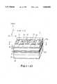
- FIGS. 1A and 1BA description is given to a first embodiment of an LED array 1 of the present invention referring to FIGS. 1A and 1B.
- FIG. 1(A)is a perspective view showing a first embodiment of an LED array of the present invention.
- FIG. 1(B)is a side sectional view taken along line A--A in FIG. 1(A) of the LED array of the present invention. Referring to FIGS. 1(A) and 1(B), the LED array 1 has a plurality of LEDs 1a aligned in row.
- Each of the plurality of the LEDs 1acomprises an n-type GaAs substrate (referred to as substrate crystal) 2, an n-type GaAs buffer layer 3, a reflecting layer 4, an n-type Al 0 .7 Ga 0 .3 As clad layer 5, a p-type Al 0 .3 Ga 0 .7 As light emitting layer 6, a p-type Al 0 .7 Ga 0 .3 As clad layer 7 and a p-type GaAs cap layer 8. These layers are stacked on the substrate crystal 2 in this order.
- An SiN insulating layer 9is formed on the surface of the positive-type isolating mesa groove 17 for protection of the surface thereof.
- the LED array of the present inventionhas a double hereto-structure having the p-type Al 0 .3 Ga 0 .7 As light emitting layer 6 interposed between the n-type and P-type Al 0 .7 Ga 0 .3 As clad layers 5 and 7.
- the reflecting layer 4is made of a plurality semi-conductive layers which have a wider forbidden band width than that of the p-type Al 0 .3 Ga 0 .7 As light emitting layer 6 and the same conductive type as the substrate crystal 2 and different refractive indexes of more than 2 kinds thereof.
- this LED array 1having the abovementioned structure, when a current is applied across the electrodes 10, 11 of the LED 1a, a light is emitted from the p-type Al 0 .3 Ga 0 .7 As light emitting layer 6 of the corresponding LED respectively. At that time, the light emitted upward from the p-type Al 0 .3 Ga 0 .7 As light emitting layer 6 is output outside from a light output surface 12, on the other hand, the light emitted downward therefrom is reflected by the reflecting layer 4 and also output outward from the light output surface 12 without being absorbed by the substrate crystal 2.
- the LED array 1 having a high light outputis obtained.
- the LED array 1having a high integration is obtained.
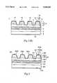
- FIGS. 2(A)-2(E)are side cross sectional views each showing a main production process of the first embodiment, taken in the direction of the ⁇ 0 -1 -1> crystal axis.
- an n-type GaAs buffer layer 3 having a thickness of 5 ⁇ mis provided on the (1 0 0) plane of an n-type GaAs substrate 2 and a reflecting layer 4 having 25 pairs of stacked layers, each pair comprising an n-type Al 0 .45 Ga 0 .55 As layer having a thickness of 50 nm and an n-type AlAs layer having a thickness of 57 nm, wherein a total thickness d of the n-type GaAs buffer layer 3 is chosen so that a central wavelength of the reflection thereof is approximately the same as a central wavelength of a peak light output of the LED 1a.
- this thickness d of the reflection layer 4is given as follows:
- na refractive index of the reflecting layer
- ⁇ pthe central wavelength
- the thickness d thereofis determined according to the center wavelength of the light emitted from the LED. Further, the maximum reflection of the reflecting layer 4 made of the plurality of pairs of the n-type Al 0 .45 Ga 0 .55 As layer and the n-type AlAs layer can be increased by causing the number of the pairs to increase.
- a photo-resist pattern layer 14is deposited on the cap layer 8 so that directions of a pair of grooves 17a, 17a (shown in FIG. 1(A)) for forming the LED array become respectively parallel to the ⁇ 0 -1 1> axis of the semi-conductive crystal layer 13 and directions of isolating mesa grooves 17 for separating the LED la becomes respectively vertical to the ⁇ 0 -1 1> axis.
- directions of a pair of grooves 17a, 17ashown in FIG. 1(A) for forming the LED array become respectively parallel to the ⁇ 0 -1 1> axis of the semi-conductive crystal layer 13 and directions of isolating mesa grooves 17 for separating the LED la becomes respectively vertical to the ⁇ 0 -1 1> axis.
- the reason why the isolating mesa groove 17 and the groove 17a become positive-type mesa grooveis based on such an experimental result obtained by the present inventors that when a groove is provided in a semi-conductive material by using the etching liquid of H 3 PO 4 ⁇ H 2 O 2 ⁇ H 2 O, the groove formed in the direction of the ⁇ 0 -1 1> axis becomes the positive-type mesa groove, however, the groove formed in the direction of the ⁇ 0 -1 -1> axis becomes the positive-type or negative-type mesa groove according to a p-type or n-type semi-conductor thereof.
- the direction of the LED array 1can also be made to be in the ⁇ 0 -1 -1> axis direction because the grooves provided in both the directions, i.e. the ⁇ 0 -1 -1> and ⁇ 0 -1 -1> axes, become the positive-type mesa grooves as mentioned in the above.
- an insulation layer 9 of SiNis formed on the etched surface and the cap layer 8 so as to have a thickness of 0.1 ⁇ m, then a contact hole 15 is provided on the cap layer 8 for each of the LEDs by removing a part of the insulation layer 9 by a plasma etching method.
- an Al layer 11afor p-type Al electrode 11
- a photo-resist layer 16 having an electrode patternis formed on the Al layer 11.
- arrays of p-type Al electrodes 11,are obtained by removing unnecessary parts of the Al layer 11 and the cap layer 8 by plasma-etching using Cl gas and by removing the photo-resist layer 16 after the plasma-etching.
- Each of the electrodes 11is led outside across the positive-type mesa grooves as shown in FIG. 1(A).
- an n-type electrode 10is formed thereon so as to have a thickness of 0.5 ⁇ m by evaporating an AuGeNi alloy.
- the LED array 1 shown in FIGS. 1(A) and 1B as well as in FIG. 2(D)is obtained.
- the depth of the isolating mesa groovesis to be shallower, i.e. the thickness of the semi-conductive layers 13 having the double hereto- structure is to be thinner, thus, this requires a precise thin layer control in production.
- the semi-conductive layer 13can be formed with the thickness of 20 ⁇ m by using the organic metal vapor phase growth method or the molecular beam epitaxial growth method.
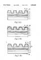
- FIG. 3is a side sectional view showing a second embodiment of a LED array.
- a feature of the second embodimentis that a reflection preventing layer 109 is provided on isolating mesa grooves 117 and a light emitting surface 112 except for electrodes 111 instead of the SiN insulation layer 9 of the LED array 1 of the first embodiment, wherein a numeral 102 designates an n-type GaAs substrate (referred to as substrate crystal), 103 an n-type GaAs buffer layer, 104 a reflecting layer, 105 an n-type Al 0 .7 Ga 0 .3 As clad layer, 106 a p-type Al 0 .3 Ga 0 .7 As GaAs light emitting layer, 107 a p-type Al 0 .7 Ga 0 .3 As clad layer, 108 a p-type GaAs cap layer, and 117 positive-type isolating mesa grooves.
- a numeral 102designates an n-type GaAs substrate (referred to as substrate crystal)
- 103an n-type
- a refractive indexis discontinuous at a boundary surface between an outside and an inside of the semi-conductive crystal surface, so that a loss of the light output occurs because the light reflected by the boundary surface interfere with the lights emitted from the p-type Al 0 .3 Ga 0 .7 As light emitting layer 106.
- the reflection preventing layer 109 in this embodimentis provided to prevent the light from being reflected by the boundary surface 112 by utilizing light wave interference.
- the reflection preventing layer 109is formed with SiN by a vapor phase growth method so as to have a thickness d satisfying following conditions:
- dthe thickness of the reflection preventing layer 109
- ma positive integer
- ⁇ pa center wavelength of the light emitted from an LED 101a
- na refractive index of the reflection preventing layer 109.
- the thickness d of the reflection preventing layer 109is determined according to the above condition (2), the light having a center wavelength ⁇ p is efficiently output outward, i.e. the light is prevented from being reflected by providing the reflection preventing layer 109 on the light output surface 112 of the LED 101a.
- FIG. 4is a graph of emission spectrum of the LED array of the second embodiment.
- FIG. 5is a graph of emission spectrum of the LED array of the first embodiment.
- the periodic loss of the light output with respect to the wavelengthis minimized compared with that of the LED array 1 of the first embodiment.
- the reflected light from the light output surface 112can be reduced to the minimum and the light emitting efficiently of the LED array 101 can be increased by providing the reflection preventing layer 109 on the light output surface 112.
- the reflection preventing layer 109is provided not only on the light output surface 112 but also on the isolating mesa grooves 17, thus, it serves as an antioxidant layer for the semi-conductive layers forming the LED array 101.
- FIG. 6is a side sectional view of a third embodiment of an LED array of the present invention.
- a feature of the LED array 201 of this third embodimentis that an upper portion of the p-type Al 0 .7 Ga 0 .3 As clad layer 7 of the first embodiment, i.e. a contact portion with the p-type GaAs cap layer 8, has higher impurity concentration.
- two layerscomprising a lower impurity concentration clad layer 207a of a p-type Al 0 .7 Ga 0 .3 As layer having an impurity concentration of 8 ⁇ 10 17 cm -3 and a higher impurity concentration clad layer 207b of a p + -type Al 0 .7 Ga 0 .3 As layer having a higher impurity concentration of 3 ⁇ 10 18 cm -3 by being diffused with Zn are provided between a p-type Al 0 .3 Ga 0 .7 As light emitting layer 206 and a p-type GaAs cap layer 208 as shown in FIG.
- a numeral 202designates an n-type GaAs substrate (referred to as substrate crystal), 203 an n-type GaAs buffer layer, 204 a reflecting layer, 205 an n-type Al 0 .7 Ga 0 .3 As clad layer, 210, 211 an electrode, and 217 positive-type isolating mesa grooves.
- the impurity concentration and the thickness of the above lower and higher impurity concentration clad layers 207a and 207bare determined depending on the application of the LED array.
- the above two layers 207a and 207bare formed by the organic metal vapor phase growth method or the molecular beam epitaxitial growth method used as well as in the first embodiment.
- the lower impurity concentration clad layer 207ahas almost the same impurity concentration and conductivity as the first and second embodiments. Therefore, when a current is applied to the LED 201a, the current is diffused into the lower impurity concentration clad layer 207a, so that the emitting area of the light emitting layer 206 is extended. Thus, a high light output is obtained from the light emitting layer 206.
- the higher impurity concentration clad layer 207bhas higher impurity concentration and conductivity than those of the lower impurity concentration clad layer 207a, thus, when a current is applied to the LED 201a, no heat is generated from the higher impurity concentration clad layer 207b, which effectively decreases overall heat generation from the LED array 201.
- the decrease of overall heat generation from the LED array 201enables realizing an LED array having a high light output and a high integration.
- the lower impurity concentration clad layer 207a and the n-type Al 0 .7 Ga 0 .3 As clad layer 205have approximately the same impurity concentration and conductivity as those of the first and second embodiments.
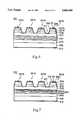
- FIG. 7is a side sectional view of a fourth embodiment of the LED array of the present invention.
- a feature of the LED array 301 of the fourth embodimentis that a multiplexed reflecting multilayer 304 is provided on an n-type GaAs buffer layer 303 instead of the reflecting layer 4 in the LED array 1 of the embodiment 1 shown in FIG.
- a numeral 302designates an n-type GaAs substrate (referred to as substrate crystal), 308 an n-type GaAs buffer layer, 305 an n-type Al 0 .7 Ga 0 .3 As clad layer, 306 a p-type Al 0 .3 Ga 0 .7 As GaAs light emitting layer, 307 a p-type Al 0 .7 Ga 0 .3 As clad layer, 808 a p-type GaAs cap layer, and 317 positive-type isolating mesa grooves.
- substrate crystaldesignates an n-type GaAs substrate (referred to as substrate crystal)
- 308an n-type GaAs buffer layer
- 305an n-type Al 0 .7 Ga 0 .3 As clad layer
- 306a p-type Al 0 .3 Ga 0 .7 As GaAs light emitting layer
- the multiplexed reflecting multilayer 304comprises a first reflecting multilayer 304a made of plural semi-conductive layers of different kind materials having different refraction indexes, of which layer thicknesses are intentionally changed, and a second reflecting multilayer 304b made of plural semi-conductive layers of the same kind materials as the first reflecting multilayer 304a and each of the semi-conductive layer thereof has a different thickness from those of the first reflecting multilayer 304a.
- the first reflecting multilayer 304ais made by stacking 25 layer pairs, of which each pair comprises an Al 0 .35 Ga 0 .65 As semi-conductive layer having a thickness of 53 nm and an Al 0 .8 Ga 0 .2 As semi-conductive layer having a thickness of 57 nm
- the second reflecting multilayer 304bis provided by stacking 25 layer pairs of which each pair comprises an Al 0 .35 Ga 0 .65 As semi-conductive layer having a thickness of 48 nm and an Al 0 .8 Ga 0 .2 As semi-conductive layer having a thickness of 53 nm, wherein a refraction index of the Al 0 .35 Ga 0 .65 As semi-conductive layer is different from that of the Al 0 .8 Ga.sub..2 As semi-conductive layer.
- the first and second reflecting multilayers 304a and 304brespectively have a reflecting center wavelength of 720 nm and that of 687 nm because the thickness of each of components of the first reflecting multilayer 304a is different from that of each of components of the second reflecting multilayer 304b.
- FIG. 8(A)is a graph showing a reflecting spectrum of the multiplexed reflecting multilayer 304 of the LED array 301 of the fourth embodiment.
- FIG. 8(B)is a graph showing a reflective spectrum of the reflecting layer 4 of the LED array 1 of the first embodiment.
- the reflective spectrum of the multiplexed reflecting multilayer 304 of the LED array 301has a wider half width of 90 nm at a reflective center wavelength of 700 nm compared with that of the LED array 1 of the first embodiment shown in FIG. 1 at the reflective center wavelength of 700 nm.
- the reflective spectrum of the multiplexed reflecting multilayer 304has a combined the reflective spectrums of the first and second reflecting multilayers 304a and 304b.
- the thickness d of the first or second reflecting multilayer 304a or 304bis determined by the condition
- each thickness d of the first and second reflecting multilayers 304a and 304bis chosen so that the composed reflective spectrum forms a flat top at the most intensive reflecting part when both the first and second reflecting multilayers 304a and 304b are provided as the multiplexed reflecting multilayer 304.
- the LED array 301it is possible for the LED array 301 to increase the light output in a whole wavelength range of the light emitted from the light emitting layer 306 thereof.
- a degradation of the light outputdoes not occur in spite of a deviation of thickness of the multiplexed reflecting multilayer 304 in a production process because of the wider half width of spectrum range.
- a double reflecting multilayersis employed as the multiplexed reflecting multilayer 304, however, it is possible to employ a multiplexed reflecting multilayer having more than two reflecting multilayers by causing a reflective center wavelength of each of the reflecting multi layers to be different from each other, so that a multiplexed reflecting multilayer having a wider half width of spectrum range can be obtained.
- FIG. 9is a side sectional view showing a fifth embodiment of the LED array.
- the feature of the fifth embodiment of the LED array 401is that in the first embodiment of the LED array 1, the isolating mesa groove 17 thereof is provided so as to penetrate partially into the n-type Al 0 .7 Ga 0 .3 As clad layer 5 by etching.
- an isolating mesa groove 417 formed in the LED array 401 of the fifth embodimentcomprises a positive-type mesa groove from a light output surface 412 to a p-n junction plane 418 formed between a p-type Al 0 .3 Ga 0 .7 As light emitting layer 406 and a p-type Al 0 .7 Ga 0 .3 As clad layer 407, and a negative-type mesa groove penetrating from the p-n junction plane 418 into a part of an n-type Al 0 .7 Ga 0 .3 As clad layer 405, wherein a numeral 402 designates an n-type GaAs substrate (referred to as substrate crystal), 403 an n-type GaAs buffer layer, 404 a reflecting layer, 406 a p-type Al 0 .3 Ga 0 .7 As GaAs light emitting layer, 407 a p-type Al 0 .7 Ga
- the abovementioned configuration of the isolating mesa groove 417is based on such an experimental result obtained by the present inventors that when a groove is formed in a semi-conductive material by using the etching liquid of H 3 PO 4 ⁇ H 2 O 2 ⁇ H 2 O, the groove formed in the direction of the ⁇ 0 -1 1> axis becomes the positive-type mesa groove, however, the groove formed in the direction of the ⁇ 0 -1 -1> axis becomes the positive-type or negative-type mesa groove according to a p-type or n-type semi-conductor thereof as mentioned in the foregoing.
- FIG. 10is a side sectional view showing the sixth embodiment of the LED array.
- the feature of the sixth embodiment of the LED array 501is that in the first embodiment of the LED array 1, the isolating mesa groove 17 thereof is provided so as to have a vertical wall.
- an isolating mesa groove 517 of the sixth embodiment of an LED array 501has a vertical wall, wherein a numeral 502 designates an n-type GaAs substrate (referred to as substrate crystal), 503 an n-type GaAs buffer layer, 504 a reflecting layer, 505 an n-type Al 0 .7 Ga 0 .3 As clad layer, 506 a p-type Al 0 .3 Ga 0 .7 As GaAs light emitting layer, 507 a p-type Al 0 .7 Ga 0 .3 As clad layer, 508 a p-type GaAs cap layer, and 510, 511, electrodes.
- a numeral 502designates an n-type GaAs substrate (referred to as substrate crystal)
- 503an n-type GaAs buffer layer
- 504 a reflecting layer505 an n-type Al 0 .7 Ga 0 .3 As clad layer
- 506
- the isolating mesa groove 517 having the vertical wallis produced by changing the production processes of the first embodiment shown in FIGS. 2(B)-2(E) as follows:
- FIG. 11(A)is a perspective view showing a main production process of the sixth embodiment of the LED array 501.
- FIGS. 11(B)-11(F)are side sectional views each showing a main production process of the sixth embodiment of the LED array.
- FIG. 11(A)the same layers as those of the sixth embodiment shown in FIG. 10 are provided as shown in FIG. 11(A).
- a photo-resist pattern layer 514ais formed on the p-type GaAs cap layer 508 of the stacked wafer so that an array direction of the LED array 501 becomes parallel to the ⁇ 0 -1 1> crystal axis.
- the abovementioned groovesbecome a positive-type etched grooves when a etching liquid other than the H 3 PO 4 ⁇ H 2 O 2 ⁇ H 2 O is used.
- a photo-resist pattern 514bis again deposited thereon as shown in FIG. 11(B).
- the stacked waferis etched by the plasma etching using Cl 2 gas, thus, the isolating mesa grooves 517 having the vertical walls are obtained as shown in FIG. 11(C).
- an insulation layer 509 of SiNis formed on the etched surface and the cap layer 508 so as to have a thickness of 0.1 ⁇ m, then a contact hole 515 is provided on the cap layer 508 of each of the LEDs 501a shown in FIG. 11(F) by removing a part of the insulation layer 509 by a plasma etching method.
- Al electrode 511Al electrode 511
- a photo-resist layer 516 having electrode patternis formed on the Al layer 511a.
- p-type Al electrodes 511each led outside across the positive-type groove provided in the direction of the LED array 501 therein, are obtained by plasma-etching the Al layer 511 and the cap layer 508 using Cl 2 gas and by removing the photo-resist layer 516 after the plasma etching.
- an n-type electrode 510is formed thereon so as to have a thickness of 0.5 ⁇ m by evaporating an AuGeNi alloy.
- the LED array 501 shown in FIG. 10 as well as in FIG. 11(F)is obtained.
- FIG. 12is a side sectional view showing a seventh embodiment of an LED array of the present invention.
- a feature of the seventh embodiment of the LED array 601is that the isolating mesa groove 17 of the LED array 1 of the first embodiment is further extended to a boundary surface between the reflecting layer 4 and the substrate crystal 2 (or the buffer layer 5) of the first embodiment.
- isolating mesa grooves 617 of the seventh embodimentare provided so as to reach a boundary surface between the reflecting multilayer 604 and the buffer layer 603, wherein a numeral 602 designates an n-type GaAs substrate crystal, 603 an n-type GaAs buffer layer, 604 a reflecting multilayer, 605 an n-type Al 0 .7 Ga 0 .3 As clad layer, 606 a p-type Al 0 .3 Ga 0 .7 As GaAs light emitting layer, 607 a p-type Al 0 .7 Ga 0 .3 As clad layer, 608 a p-type GaAs cap layer, and 610, 611, electrodes.
- a numeral 602designates an n-type GaAs substrate crystal
- 603an n-type GaAs buffer layer
- 604 a reflecting multilayer605 an n-type Al 0 .7 Ga 0 .3 As clad layer
- the each of the isolating mesa grooves 617is obtained by etching the stacked wafer until the isolating mesa groove 617 (17) reaches the boundary surface between the reflecting multilayer 604 and the buffer layer 603 through the n-type Al 0 .7 Ga 0 .3 As clad layer 605 and the reflecting layer 604 in the etching process of the first embodiment shown in FIG. 2(B).
- the n-type GaAs buffer layer 603(the substrate crystal 602), however, is not etched because the composition thereof is different from the others.
- the isolating mesa grooves 617have uniform depths, so that each of the LEDs has an uniform and high light emitting output.
Landscapes
- Led Devices (AREA)
Abstract
Description
1. Field of the Invention
The present invention relates to a light emitting diode array, in particular, to an improvement of a monolithic light emitting diode array having a plurality of surface light emitting diodes having a mesa structure aligned in row, and to the production method of the light emitting diode array.
2. Description of the Related Art
Presently, in order to utilize light emitting diodes (referred to as LEDs hereafter) as a light source for a printer utilizing a light and for an information writing element of an optical information device, there are proposed or developed many techniques for integrating a plurality of LEDs into a monolithic LED array (referred to as LED array hereafter) in a high integration.
The LED array is provided with an array of LEDs having an integration of, for instance, 300-400 dpi (dots per inch) by causing the LEDs to be lineally aligned in row, however, the LED array is further required to have a higher integration because of demands for down-sizing of the light utilizing printer and for a high definition picture of the optical information device.
In order to realize an LED array having an integration of more than 1600 dpi, the LEDs have to be aligned in row at a pitch of less than 16 μm on a substrate crystal. As a method for electrically isolating the LEDs from each other, there is proposed such a method as providing isolating mesa grooves between the LEDs by using an etching liquid or such a method as diffusing impurity elements to form diffusion areas between the LEDs.
In the above etching method and impurity diffusion method, the isolating mesa grooves and the diffusion areas are spread not only in directions of depths thereof but also in lateral directions thereof, so that the grooves and the diffusion areas have to be formed in the depths of less than 3 μm. The technique for isolating the LEDs from each other by the impurity diffusion method is disclosed in Japanese Laid-Open Publication 2382/1984.
In the production method of the prior art, at first, a p-type GaAlAs layer and an n-type GaAlAs layer are formed on a substrate crystal in this order by a liquid phase growth method. Thus, a semi-conductive wafer is obtained. Next, after an insulation layer, for instance, of SiO2 is formed on the semi-conductor wafer, one part of the insulation layer is removed by using a photolithography leaving another part thereof corresponding to the light emitting areas. Then, zinc elements are diffused into the n-type GaAlAs layer so as to reach the p-type GaAlAs layer from the surface of the wafer by causing the insulation layer to be a mask, so that p-type isolation areas are formed in the semi-conductive wafer, thus the LED array having a plurality of separated LEDs is obtained. According to the above LED array, it is possible to obtain an LED array having an aligned pitch of less than 50 μm by causing a thickness of the n-type GaAlAs on which the p-type isolation areas are formed, to be less than 10 μm.
In the above production method of the LED array, however, it was difficult to obtain the LED array having a high light emitting output because of the impurity diffusion.
Further, it was difficult to obtain the LED array having an adequately small dispersion of light emitting output because a layer having thickness of less than 10 μm can not be obtained by the liquid phase growth method without dispersion of the thickness thereof, while the liquid phase growth method is suitable to form a layer having a thickness of more than 10 μm.
Thus, the liquid phase growth method is employed to obtain a semi-conductive wafer having thick films on the substrate crystal. The thick films allow the semi-conductive wafer to remove the substrate crystal by using an etching liquid., so that a conductive layer for an electrode can be directly formed on the thick films after removing the substrate from the semi-conductive wafer. This structure of the LED array is advantageous to preventing the lights emitted from the light emitting areas from being absorbed by the substrate crystal.
Recently, new thin film forming techniques such as an organic metal vapor phase growth method and a molecular beam epitaxial growth method have been developed for forming a semi-conductive layer having a thickness of 5˜6 μm on the substrate crystal, and these techniques have realized a thin film having an uniform thickness because of excellent controllability of the thin film.
These organic metal vapor phase growth method and molecular beam epitaxial growth method have the excellent controllability of the thin films formed on the substrate crystal, however, they are not suitable for forming the thin films having thicknesses of more than 10 μm on the contrary. Therefore, the conductive layer for electrode of the LED array has to be provided on the surface of the substrate crystal on which the thin films are formed because the thin films formed by the above methods are too thin or mechanically too weak to remove the substrate crystal from the semi-conductive wafer leaving thin films by using an etching liquid. This poses a loss of light emitting output because lights emitted from the diodes are mostly absorbed by the substrate crystal.
Further, in the prior art, in order to form the isolating mesa grooves between the emitting diodes, a mesa etching method using the etching liquid is employed.
When an isolating mesa groove is formed in a direction of a <0 -1 -1> axis of a crystal semi-conductor on a (1 0 0) plane by a mesa etching using HCl liquid, edge angles formed at side walls of the isolating mesa groove have acute angles or negative slopes (the groove having walls of the negative slopes is referred to as a negative-type mesa groove hereafter). On the other hand, when an isolating mesa groove is formed in a direction of a <0 -1 1> axis of the crystal on the (1 0 0) plane by the mesa etching, edge angles formed at side walls of the isolating mesa groove have obtuse angles or positive slopes (the groove having walls of positive slopes is referred to as a positive-type mesa groove hereafter).
Thus, when a direction of the LEDs aligned in row, i.e. a direction of an LED array, is defined in parallel with the <0 -1 1> axis of the crystal, the isolating mesa groove formed in parallel with the direction of the LED array becomes the positive-type mesa groove. On the other hand, a crystal axis vertical to the <0 -1 1> axis becomes a <0 -1 -1>, thus, the isolating mesa grooves for dividing an LED array portion to an individual LED become the negative-type mesa grooves.
As mentioned in the above, the isolating mesa grooves of the LEDs array have the negative-type grooves, thus, the deeper the depths of the negative-type grooves, the smaller the areas at the feet of the LEDs through which a current follows, so that each of the LEDs has a large resistance, which poses a cause of decrease of light emitting output.
Generally, upon a mass-production of the LED arrays, an electrode is formed on a top surface of each of the LEDs by forming an electrode pattern on a wafer made of semi-conductive layer using plasma etching. At first, an electrode layer is provided on the wafer having the isolating mesa grooves provided in advance by evaporating electrode material, then, the electrode layer except for parts provided on the top of LEDs is removed from the wafer by the plasma etching using a mask pattern. At that time, the electrode layer formed on the slopes and parts under the slopes in the negative-type grooves is apt to be left thereon because of shade of the LED portion, which poses a cause of short circuit. b
Accordingly, a general object of the present invention is to provide an LED array in which the above disadvantages have been eliminated.
A more specific object of the present invention is to provide an LED array having a high light emitting output by providing a reflecting layer on the side of the substrate crystal, which reflecting layer reflects lights travelling in a direction of a substrate crystal from a light emitting layer.
Another specific object of the present invention is to provide an LED array having a high integration and generating less heat by adopting thin semi-conducting layers constructing a double hereto-structure owing to the provision of the reflecting layer.
Other specific object of the present invention is to provide an LED array having a high light emitting output by employing the reflecting layer having a wide reflective spectrum coverring an entire light wavelength of the lights emitted from the LED array.
Further, other specific object of the present invention is to provide a light emitting diode array comprising, a substrate crystal made of a conductive-type semi-conductor, a plurality of light emitting diodes aligned in row on the substrate crystal, each of the light emitting diodes having a light output surface from which a light is emitted outside, and being isolated with isolating mesa grooves, and having a double hereto-structure formed by causing a light emitting layer having a forbidden band width to be interposed with different conductive-type semi-conductive layers and a reflecting layer provided between the substrate crystal and one of the different conductive-type semi-conductive layers, the reflecting layer comprising a plurality of semi-conductive layers having 2 or more kinds of different refractive indexes, each of the semi-conductive layers made of the same conductive-type semi-conductor as that of the substrate crystal and having a wider forbidden band width than that of the light emitting layer.
Further, other specific object of the present invention is to provide a production method for producing a light emitting diode array, comprising the steps of, forming a reflecting layer and semi-conductive layers having a double hereto-structure on a substrate crystal, providing parallel grooves defined as positive-type mesa grooves in parallel direction with a direction of the light emitting diode array aligned in row and isolating mesa grooves being defined as positive-type mesa grooves for isolating light emitting diodes in the array from each other in a direction vertical to the direction of the light emitting diode array by wet etching using an etching liquid comprising H3 PO4 ·H2 O2 having volume ratio of H3 PO4 : H2 O2 =1˜5:1 and H2 O having a predetermined volume ratio, and providing electrodes on the light emitting diodes.
Other objects and further features of the present invention will be apparent from the following detailed description when read in conjunction with the accompanying drawings.
Preferred examples of the present invention will be described with reference to the accompanying drawings wherein:
FIG. 1(A) is a perspective view showing a first embodiment of an LED array of the present invention.
FIG. 1(B) is a side sectional view taken along line A--A in FIG. 1(A).
FIGS. 2(A)-2(E) are side cross sectional views each showing a main production process of the first embodiment, taken in the direction of the <0 -1 -1> crystal axis.
FIG. 3 is a side sectional view showing a second embodiment of a LED array of the present invention.
FIG. 4 is a graph of emission spectrum of the LED array of the second embodiment.
FIG. 5 is a graph of emission spectrum of the LED array of the first embodiment.
FIG. 6 is a side sectional view of a third embodiment of a LED array of the present invention.
FIG. 7 is a side sectional view of a fourth embodiment of the LED array of the present invention.
FIG. 8(A) is a graph showing a reflective spectrum of the multiple reflecting multilayer of the LED array of the fourth embodiment.
FIG. 8(B) is a graph showing a reflective spectrum of the reflecting layer of the LED array of the first embodiment.
FIG. 9 is a side sectional view showing a fifth embodiment of the LED array of the present invention
FIG. 10 is a side sectional view showing the sixth embodiment of the LED array of the present invention.
FIG. 11(A) is a perspective view showing a main production process of the sixth embodiment of theLED array 501.
FIGS. 11(B)-11(F) are side sectional views each showing a main production process of the sixth embodiment of the LED array.
FIG. 12 is a side sectional view showing a seventh embodiment of an LED array of the present invention.
A description is given to a first embodiment of anLED array 1 of the present invention referring to FIGS. 1A and 1B.
FIG. 1(A) is a perspective view showing a first embodiment of an LED array of the present invention.
FIG. 1(B) is a side sectional view taken along line A--A in FIG. 1(A) of the LED array of the present invention. Referring to FIGS. 1(A) and 1(B), theLED array 1 has a plurality ofLEDs 1a aligned in row. Each of the plurality of theLEDs 1a comprises an n-type GaAs substrate (referred to as substrate crystal) 2, an n-typeGaAs buffer layer 3, a reflectinglayer 4, an n-type Al0.7 Ga0.3 As cladlayer 5, a p-type Al0.3 Ga0.7 Aslight emitting layer 6, a p-type Al0.7 Ga0.3 As cladlayer 7 and a p-typeGaAs cap layer 8. These layers are stacked on thesubstrate crystal 2 in this order. Positive-type isolatingmesa grooves 17 each penetrating partially into the n-type Al0.7 Ga0.3 As cladlayer 5 through the p-typeGaAs cap layer 8 are provided between the LEDs la, la so as to form a plurality ofLEDs 1a in row. AnSiN insulating layer 9 is formed on the surface of the positive-type isolatingmesa groove 17 for protection of the surface thereof. On the p-type cap layer 8 of each of theLEDs 1a and the bottom of thesubstrate crystal 2 there provided anAl electrode 11 and anAuGeNi electrode 10 respectively. Thus, the LED array of the present invention has a double hereto-structure having the p-type Al0.3 Ga0.7 Aslight emitting layer 6 interposed between the n-type and P-type Al0.7 Ga0.3 As cladlayers
The reflectinglayer 4 is made of a plurality semi-conductive layers which have a wider forbidden band width than that of the p-type Al0.3 Ga0.7 Aslight emitting layer 6 and the same conductive type as thesubstrate crystal 2 and different refractive indexes of more than 2 kinds thereof.
In thisLED array 1 having the abovementioned structure, when a current is applied across theelectrodes LED 1a, a light is emitted from the p-type Al0.3 Ga0.7 Aslight emitting layer 6 of the corresponding LED respectively. At that time, the light emitted upward from the p-type Al0.3 Ga0.7 Aslight emitting layer 6 is output outside from alight output surface 12, on the other hand, the light emitted downward therefrom is reflected by the reflectinglayer 4 and also output outward from thelight output surface 12 without being absorbed by thesubstrate crystal 2.
Thus, according to the first embodiment, theLED array 1 having a high light output is obtained.
Further, it is possible to decrease thickness of thesemi-conductive layers 13 comprising the double heterostructure, which thickness is proportional to the light output of theLED 1a, because of the high light output of theLED array 1 by providing the reflectinglayer 4, which thickness enables a narrower width of the isolatingmesa groove 17, thus theLED array 1 having a high integration is obtained.
Next, a description is given to the production method of theLED array 1 referring to FIGS. 2(A)-2(E).
FIGS. 2(A)-2(E) are side cross sectional views each showing a main production process of the first embodiment, taken in the direction of the <0 -1 -1> crystal axis.
At first, an n-typeGaAs buffer layer 3 having a thickness of 5 μm is provided on the (1 0 0) plane of an n-type GaAs substrate 2 and a reflectinglayer 4 having 25 pairs of stacked layers, each pair comprising an n-type Al0.45 Ga0.55 As layer having a thickness of 50 nm and an n-type AlAs layer having a thickness of 57 nm, wherein a total thickness d of the n-typeGaAs buffer layer 3 is chosen so that a central wavelength of the reflection thereof is approximately the same as a central wavelength of a peak light output of theLED 1a.
Generally, this thickness d of thereflection layer 4 is given as follows:
d=λp/(4n) (1)
wherein n: a refractive index of the reflecting layer, λp: the central wavelength.
In other words, the thickness d thereof is determined according to the center wavelength of the light emitted from the LED. Further, the maximum reflection of the reflectinglayer 4 made of the plurality of pairs of the n-type Al0.45 Ga0.55 As layer and the n-type AlAs layer can be increased by causing the number of the pairs to increase.
In this embodiment, 25 pairs of the stacked layers are employed according to experimental results.
Next, an n-type Al0.7 Ga0.3 As cladlayer 5 having a thickness of 5 μm, a p-type Al0.3 Ga0.7 Aslight emitting layer 6 having a thickness of 0.5 μm, a p-type Al0.7 Ga0.3 As cladlayer 7 having a thickness of 2 μm and a p-typeGaAs cap layer 8 having a thickness of 0.1 μm are respectively formed on the reflectinglayer 4 in this order by the organic metal vapor phase growth method or the molecular beam epitaxial growth method, thus asemi-conductive crystal layer 13 comprising the n-type Al0.7 Ga0.3 As cladlayer 5, the p-type Al0.3 Ga0.7 Aslight emitting layer 6 and the p-type Al0.7 Ga0.3 As cladlayer 7, is formed as a double hereto- structure.
Next, a photo-resistpattern layer 14 is deposited on thecap layer 8 so that directions of a pair ofgrooves semi-conductive crystal layer 13 and directions of isolatingmesa grooves 17 for separating the LED la becomes respectively vertical to the <0 -1 1> axis. Next, as shown in FIG. 2(B), thesemi-conductive crystal layer 13 having the photo-resistor pattern layer 14 is etched by using an etching liquid of H3 PO4 ·H2 O2 ·H2 O (volume ratio H3 PO4 :H2 O2 :H2 O=3:1:50) so that thegrooves mesa grooves 17 reach the n-type Al0.7 Ga0.3 As cladlayer 5 through the p-typeGaAs cap layer 8, thus, thegrooves 17a provided in the array direction parallel to the <0 -1 1> axis become positive-type mesa grooves and the isolatingmesa grooves 17 between the LED in the direction of the <0 -1 -1>, i.e. in the direction vertical to the <0 -1 1>, become also positive-type mesa grooves.
The reason why the isolatingmesa groove 17 and thegroove 17a become positive-type mesa groove is based on such an experimental result obtained by the present inventors that when a groove is provided in a semi-conductive material by using the etching liquid of H3 PO4 ·H2 O2 ·H2 O, the groove formed in the direction of the <0 -1 1> axis becomes the positive-type mesa groove, however, the groove formed in the direction of the <0 -1 -1> axis becomes the positive-type or negative-type mesa groove according to a p-type or n-type semi-conductor thereof.
It should be noted that the direction of theLED array 1 can also be made to be in the <0 -1 -1> axis direction because the grooves provided in both the directions, i.e. the <0 -1 -1> and <0 -1 -1> axes, become the positive-type mesa grooves as mentioned in the above.
Next, as shown in FIG. 2(C), after removing thephotoresist 14, aninsulation layer 9 of SiN is formed on the etched surface and thecap layer 8 so as to have a thickness of 0.1 μm, then acontact hole 15 is provided on thecap layer 8 for each of the LEDs by removing a part of theinsulation layer 9 by a plasma etching method.
Next, referring to FIG. 2(D), after anAl layer 11a (for p-type Al electrode 11) is deposited thereon so as to have a thickness of 0.5 μm by the vacuum evaporation method, a photo-resistlayer 16 having an electrode pattern is formed on theAl layer 11. Then, arrays of p-type Al electrodes 11, are obtained by removing unnecessary parts of theAl layer 11 and thecap layer 8 by plasma-etching using Cl gas and by removing the photo-resistlayer 16 after the plasma-etching. Each of theelectrodes 11 is led outside across the positive-type mesa grooves as shown in FIG. 1(A).
Next, referring to FIG. 2(E), after grinding a bottom of thesubstrate crystal 2, an n-type electrode 10 is formed thereon so as to have a thickness of 0.5 μm by evaporating an AuGeNi alloy. Thus, theLED array 1 shown in FIGS. 1(A) and 1B as well as in FIG. 2(D) is obtained.
Generally, in order to narrow the pitch between the LEDs in an LED array, it is required that the depth of the isolating mesa grooves is to be shallower, i.e. the thickness of thesemi-conductive layers 13 having the double hereto- structure is to be thinner, thus, this requires a precise thin layer control in production.
In the above embodiment, thesemi-conductive layer 13 can be formed with the thickness of 20 μm by using the organic metal vapor phase growth method or the molecular beam epitaxial growth method.
A description is given to a second embodiment of an LED array of the present invention referring to FIG. 3.
FIG. 3 is a side sectional view showing a second embodiment of a LED array.
A feature of the second embodiment is that areflection preventing layer 109 is provided on isolatingmesa grooves 117 and alight emitting surface 112 except forelectrodes 111 instead of theSiN insulation layer 9 of theLED array 1 of the first embodiment, wherein a numeral 102 designates an n-type GaAs substrate (referred to as substrate crystal), 103 an n-type GaAs buffer layer, 104 a reflecting layer, 105 an n-type Al0.7 Ga0.3 As clad layer, 106 a p-type Al0.3 Ga0.7 As GaAs light emitting layer, 107 a p-type Al0.7 Ga0.3 As clad layer, 108 a p-type GaAs cap layer, and 117 positive-type isolating mesa grooves.
In theLED array 1 of the first embodiment shown in FIG. 1, a refractive index is discontinuous at a boundary surface between an outside and an inside of the semi-conductive crystal surface, so that a loss of the light output occurs because the light reflected by the boundary surface interfere with the lights emitted from the p-type Al0.3 Ga0.7 Aslight emitting layer 106. Thereflection preventing layer 109 in this embodiment, is provided to prevent the light from being reflected by theboundary surface 112 by utilizing light wave interference.
Thereflection preventing layer 109 is formed with SiN by a vapor phase growth method so as to have a thickness d satisfying following conditions:
d=(2m-1)·λp/(4·n) (2)
wherein d: the thickness of thereflection preventing layer 109, m: a positive integer, λp: a center wavelength of the light emitted from anLED 101a and n: a refractive index of thereflection preventing layer 109.
When the thickness d of thereflection preventing layer 109 is determined according to the above condition (2), the light having a center wavelength λp is efficiently output outward, i.e. the light is prevented from being reflected by providing thereflection preventing layer 109 on thelight output surface 112 of theLED 101a.
FIG. 4 is a graph of emission spectrum of the LED array of the second embodiment.
FIG. 5 is a graph of emission spectrum of the LED array of the first embodiment.
As seen from FIGS. 4 and 5, in theLED array 101 of the second embodiment, the periodic loss of the light output with respect to the wavelength is minimized compared with that of theLED array 1 of the first embodiment. Thus, the reflected light from thelight output surface 112 can be reduced to the minimum and the light emitting efficiently of theLED array 101 can be increased by providing thereflection preventing layer 109 on thelight output surface 112.
Further, in the second embodiment, thereflection preventing layer 109 is provided not only on thelight output surface 112 but also on the isolatingmesa grooves 17, thus, it serves as an antioxidant layer for the semi-conductive layers forming theLED array 101.
Next, a description is given to a third embodiment of anLED array 201 referring to FIG. 6.
FIG. 6 is a side sectional view of a third embodiment of an LED array of the present invention.
A feature of theLED array 201 of this third embodiment is that an upper portion of the p-type Al0.7 Ga0.3 As cladlayer 7 of the first embodiment, i.e. a contact portion with the p-typeGaAs cap layer 8, has higher impurity concentration.
In other wards, in theLED array 201 of this embodiment, two layers comprising a lower impurity concentration cladlayer 207a of a p-type Al0.7 Ga0.3 As layer having an impurity concentration of 8×1017 cm-3 and a higher impurity concentration cladlayer 207b of a p+ -type Al0.7 Ga0.3 As layer having a higher impurity concentration of 3×1018 cm-3 by being diffused with Zn are provided between a p-type Al0.3 Ga0.7 Aslight emitting layer 206 and a p-typeGaAs cap layer 208 as shown in FIG. 6, wherein a numeral 202 designates an n-type GaAs substrate (referred to as substrate crystal), 203 an n-type GaAs buffer layer, 204 a reflecting layer, 205 an n-type Al0.7 Ga0.3 As clad layer, 210, 211 an electrode, and 217 positive-type isolating mesa grooves.
The impurity concentration and the thickness of the above lower and higher impurity concentration cladlayers
The above twolayers
The lower impurity concentration cladlayer 207a has almost the same impurity concentration and conductivity as the first and second embodiments. Therefore, when a current is applied to theLED 201a, the current is diffused into the lower impurity concentration cladlayer 207a, so that the emitting area of thelight emitting layer 206 is extended. Thus, a high light output is obtained from thelight emitting layer 206.
Further, the higher impurity concentration cladlayer 207b has higher impurity concentration and conductivity than those of the lower impurity concentration cladlayer 207a, thus, when a current is applied to theLED 201a, no heat is generated from the higher impurity concentration cladlayer 207b, which effectively decreases overall heat generation from theLED array 201.
The decrease of overall heat generation from theLED array 201 enables realizing an LED array having a high light output and a high integration.
It is noted that the lower impurity concentration cladlayer 207a and the n-type Al0.7 Ga0.3 As cladlayer 205 have approximately the same impurity concentration and conductivity as those of the first and second embodiments.
Next, a description is given to a fourth embodiment of theLED array 301 referring to FIG. 7.
FIG. 7 is a side sectional view of a fourth embodiment of the LED array of the present invention. Referring to FIG. 7, a feature of theLED array 301 of the fourth embodiment is that a multiplexed reflecting multilayer 304 is provided on an n-typeGaAs buffer layer 303 instead of the reflectinglayer 4 in theLED array 1 of theembodiment 1 shown in FIG. 1, wherein a numeral 302 designates an n-type GaAs substrate (referred to as substrate crystal), 308 an n-type GaAs buffer layer, 305 an n-type Al0.7 Ga0.3 As clad layer, 306 a p-type Al0.3 Ga0.7 As GaAs light emitting layer, 307 a p-type Al0.7 Ga0.3 As clad layer, 808 a p-type GaAs cap layer, and 317 positive-type isolating mesa grooves.
The multiplexed reflecting multilayer 304 comprises a first reflectingmultilayer 304a made of plural semi-conductive layers of different kind materials having different refraction indexes, of which layer thicknesses are intentionally changed, and a second reflecting multilayer 304b made of plural semi-conductive layers of the same kind materials as the first reflectingmultilayer 304a and each of the semi-conductive layer thereof has a different thickness from those of the first reflectingmultilayer 304a.
For instance, the first reflectingmultilayer 304a is made by stacking 25 layer pairs, of which each pair comprises an Al0.35 Ga0.65 As semi-conductive layer having a thickness of 53 nm and an Al0.8 Ga0.2 As semi-conductive layer having a thickness of 57 nm, and the second reflecting multilayer 304b is provided by stacking 25 layer pairs of which each pair comprises an Al0.35 Ga0.65 As semi-conductive layer having a thickness of 48 nm and an Al0.8 Ga0.2 As semi-conductive layer having a thickness of 53 nm, wherein a refraction index of the Al0.35 Ga0.65 As semi-conductive layer is different from that of the Al0.8 Ga.sub..2 As semi-conductive layer.
The first and second reflectingmultilayers 304a and 304b respectively have a reflecting center wavelength of 720 nm and that of 687 nm because the thickness of each of components of the first reflectingmultilayer 304a is different from that of each of components of the second reflecting multilayer 304b.
FIG. 8(A) is a graph showing a reflecting spectrum of the multiplexed reflecting multilayer 304 of theLED array 301 of the fourth embodiment.
FIG. 8(B) is a graph showing a reflective spectrum of the reflectinglayer 4 of theLED array 1 of the first embodiment.
As seen from FIGS. 8(A) and 8(B), in a reflective spectrum of the multiplexed reflecting multilayer 304 of theLED array 301, the reflective spectrum thereof has a wider half width of 90 nm at a reflective center wavelength of 700 nm compared with that of theLED array 1 of the first embodiment shown in FIG. 1 at the reflective center wavelength of 700 nm. Thus, it will be understood that the reflective spectrum of the multiplexed reflecting multilayer 304 has a combined the reflective spectrums of the first and second reflectingmultilayers 304a and 304b. At that time, the thickness d of the first or second reflectingmultilayer 304a or 304b is determined by the condition
d=λp/ (4n) (1)
as mentioned in the foregoing.
In addition, each thickness d of the first and second reflectingmultilayers 304a and 304b is chosen so that the composed reflective spectrum forms a flat top at the most intensive reflecting part when both the first and second reflectingmultilayers 304a and 304b are provided as the multiplexed reflecting multilayer 304.
Thus, it is possible for theLED array 301 to increase the light output in a whole wavelength range of the light emitted from thelight emitting layer 306 thereof.
Further, a degradation of the light output does not occur in spite of a deviation of thickness of the multiplexed reflecting multilayer 304 in a production process because of the wider half width of spectrum range.
It is noted that in this embodiment, a double reflecting multilayers is employed as the multiplexed reflecting multilayer 304, however, it is possible to employ a multiplexed reflecting multilayer having more than two reflecting multilayers by causing a reflective center wavelength of each of the reflecting multi layers to be different from each other, so that a multiplexed reflecting multilayer having a wider half width of spectrum range can be obtained.
Next, a description is given to a fifth embodiment of theLED array 401 of the present invention referring to FIG. 9.
FIG. 9 is a side sectional view showing a fifth embodiment of the LED array.
The feature of the fifth embodiment of theLED array 401 is that in the first embodiment of theLED array 1, the isolatingmesa groove 17 thereof is provided so as to penetrate partially into the n-type Al0.7 Ga0.3 As cladlayer 5 by etching.
Referring to FIG. 9, an isolatingmesa groove 417 formed in theLED array 401 of the fifth embodiment comprises a positive-type mesa groove from alight output surface 412 to ap-n junction plane 418 formed between a p-type Al0.3 Ga0.7 Aslight emitting layer 406 and a p-type Al0.7 Ga0.3 As cladlayer 407, and a negative-type mesa groove penetrating from thep-n junction plane 418 into a part of an n-type Al0.7 Ga0.3 As cladlayer 405, wherein a numeral 402 designates an n-type GaAs substrate (referred to as substrate crystal), 403 an n-type GaAs buffer layer, 404 a reflecting layer, 406 a p-type Al0.3 Ga0.7 As GaAs light emitting layer, 407 a p-type Al0.7 Ga0.3 As clad layer, 408 a p-type GaAs cap layer, and 410, 411, electrodes. On the other hand, a groove formed parallel to the array direction of the <0 -1 1> axis has a positive-type mesa groove.
The abovementioned configuration of the isolatingmesa groove 417 is based on such an experimental result obtained by the present inventors that when a groove is formed in a semi-conductive material by using the etching liquid of H3 PO4 ·H2 O2 ·H2 O, the groove formed in the direction of the <0 -1 1> axis becomes the positive-type mesa groove, however, the groove formed in the direction of the <0 -1 -1> axis becomes the positive-type or negative-type mesa groove according to a p-type or n-type semi-conductor thereof as mentioned in the foregoing.
Thus, when each of the isolatingmesa grooves 417 is formed in the direction of the <0 -1 -1> axis by using the etching liquid of H3 PO4 ·H2 O2 ·H2 O, a part of the isolatingmesa groove 417 penetrating from alight output surface 412 into ap-n junction plane 418 formed between a p-type Al0.3 Ga0.7 Aslight emitting layer 406 and the p-type Al0.7 Ga0.7 As cladlayer 407 becomes the positive-type mesa groove, and another part of the isolatingmesa groove 417 penetrating from thep-n junction plane 418 into the part of the n-type Al0.7 Ga0.3 As cladlayer 405 becomes the negative-type mesa groove. Thus, a drain of the p-n junction plane 18 becomes the widest, which is advantageous to increase the light output because of a low resistance of thep-n junction plane 418, and to decrease the heat generated therefrom.
Next, a description is given to a sixth embodiment of theLED array 501 referring to FIG. 10.
FIG. 10 is a side sectional view showing the sixth embodiment of the LED array.
The feature of the sixth embodiment of theLED array 501 is that in the first embodiment of theLED array 1, the isolatingmesa groove 17 thereof is provided so as to have a vertical wall.
Referring to FIG. 10, an isolatingmesa groove 517 of the sixth embodiment of anLED array 501 has a vertical wall, wherein a numeral 502 designates an n-type GaAs substrate (referred to as substrate crystal), 503 an n-type GaAs buffer layer, 504 a reflecting layer, 505 an n-type Al0.7 Ga0.3 As clad layer, 506 a p-type Al0.3 Ga0.7 As GaAs light emitting layer, 507 a p-type Al0.7 Ga0.3 As clad layer, 508 a p-type GaAs cap layer, and 510, 511, electrodes.
The isolatingmesa groove 517 having the vertical wall is produced by changing the production processes of the first embodiment shown in FIGS. 2(B)-2(E) as follows:
FIG. 11(A) is a perspective view showing a main production process of the sixth embodiment of theLED array 501.
FIGS. 11(B)-11(F) are side sectional views each showing a main production process of the sixth embodiment of the LED array.
Next, a description is given to the production method of theLED array 1 referring to FIGS. 11(A)-11(F).
At first, the same layers as those of the sixth embodiment shown in FIG. 10 are provided as shown in FIG. 11(A).
Next, as shown in FIG. 11(A), a photo-resistpattern layer 514a is formed on the p-typeGaAs cap layer 508 of the stacked wafer so that an array direction of theLED array 501 becomes parallel to the <0 -1 1> crystal axis. Then the stacked wafer is etched so as to have a groove penetrating partially into the n-type Al0.7 Ga0.3 As cladlayer 505 by using a etching liquid of H3 PO4 ·H2 O2 ·H2 O of which volume ratio is, for instance, H3 PO4 : H2 O2 : H2 O=10:3:5, thus, the grooves formed in the array direction parallel to the <0 -1 1> axis become positive-type mesa grooves as shown in FIG. 11(A).
It should be noted that the abovementioned grooves become a positive-type etched grooves when a etching liquid other than the H3 PO4 ·H2 O2 ·H2 O is used.
Next, in order to obtain the isolatingmesa grooves 517, a photo-resistpattern 514b is again deposited thereon as shown in FIG. 11(B).
Then, the stacked wafer is etched by the plasma etching using Cl2 gas, thus, the isolatingmesa grooves 517 having the vertical walls are obtained as shown in FIG. 11(C).
Next, as shown in FIG. 11(D), after removing thephotoresist 514b, aninsulation layer 509 of SiN is formed on the etched surface and thecap layer 508 so as to have a thickness of 0.1 μm, then acontact hole 515 is provided on thecap layer 508 of each of theLEDs 501a shown in FIG. 11(F) by removing a part of theinsulation layer 509 by a plasma etching method.
Next, as shown in FIG. 11(E), after anAl layer 511a (Al electrode 511) is formed thereon so as to have a thickness of 0.5 μm by the vacuum evaporation method, a photo-resistlayer 516 having electrode pattern is formed on theAl layer 511a. Then, p-type Al electrodes 511, each led outside across the positive-type groove provided in the direction of theLED array 501 therein, are obtained by plasma-etching theAl layer 511 and thecap layer 508 using Cl2 gas and by removing the photo-resistlayer 516 after the plasma etching.
Next, as shown in FIG. 11(F), after grinding a bottom of thesubstrate crystal 502, an n-type electrode 510 is formed thereon so as to have a thickness of 0.5 μm by evaporating an AuGeNi alloy. Thus, theLED array 501 shown in FIG. 10 as well as in FIG. 11(F) is obtained.
In this embodiment, it is possible to fabricate an LED array having a high integration because a distance between theLEDs 501a can be narrowed when the isolatingmesa grooves 517 having vertical walls are provided.
Next, a description is given to a seventh embodiment of anLED array 601 referring to FIG. 12.
FIG. 12 is a side sectional view showing a seventh embodiment of an LED array of the present invention.
A feature of the seventh embodiment of theLED array 601 is that the isolatingmesa groove 17 of theLED array 1 of the first embodiment is further extended to a boundary surface between the reflectinglayer 4 and the substrate crystal 2 (or the buffer layer 5) of the first embodiment.
Referring to FIG. 12, isolatingmesa grooves 617 of the seventh embodiment are provided so as to reach a boundary surface between the reflectingmultilayer 604 and thebuffer layer 603, wherein a numeral 602 designates an n-type GaAs substrate crystal, 603 an n-type GaAs buffer layer, 604 a reflecting multilayer, 605 an n-type Al0.7 Ga0.3 As clad layer, 606 a p-type Al0.3 Ga0.7 As GaAs light emitting layer, 607 a p-type Al0.7 Ga0.3 As clad layer, 608 a p-type GaAs cap layer, and 610, 611, electrodes.
The each of the isolatingmesa grooves 617 is obtained by etching the stacked wafer until the isolating mesa groove 617 (17) reaches the boundary surface between the reflectingmultilayer 604 and thebuffer layer 603 through the n-type Al0.7 Ga0.3 As cladlayer 605 and the reflectinglayer 604 in the etching process of the first embodiment shown in FIG. 2(B).
The n-type GaAs buffer layer 603 (the substrate crystal 602), however, is not etched because the composition thereof is different from the others.
Thus, the isolatingmesa grooves 617 have uniform depths, so that each of the LEDs has an uniform and high light emitting output.
Claims (10)
1. A light emitting diode array comprising:
a substrate crystal made of a first conductivity-type semi-conductor;
a plurality of light emitting diodes aligned in row on the substrate crystal, each of the light emitting diodes having a light output surface from which a light is emitted outside, and being isolated with isolating mesa grooves, and having a double hetero-structure formed by causing a light emitting layer having a forbidden band width to be interposed between a first semi-conductor layer of said first conductivity-type and a second semi-conductor layer of a second conductivity-type; and
a reflecting layer provided between the substrate crystal and one of said first and second semi-conductor layers, the reflecting layer comprising a plurality of semi-conductive layers having 2 or more different refractive indexes, each of the semi-conductive layers having the same conductivity-type as that of the substrate crystal and having a wider forbidden band width than that of the light emitting layer.
2. A light emitting diode array as claimed in claim 1, wherein a thickness of the double hetero-structure of the light emitting diode is less than 20 μm.
3. A light emitting diode array as claimed in claim 1, wherein a reflection preventing layer is provided on the light output surface, the reflection preventing layer having a maximum transmittance in accordance with a center wavelength of the light emitted from the light emitting layer.
4. A light emitting diode array as claimed in claim 3, wherein the reflection preventing layer comprises a plurality of semi-conductive layers having different kinds of refractive indexes, one of the plurality of the semi-conductive layers having a thickness d defined as
d=(2m-1)·λp/ (4·n)
wherein m: a positive integer, λp: a center wavelength of a light emitted from the light emitting layer, and n: the refractive index of the one of the plurality of the semi-conductive layer.
5. A light emitting diode array as claimed in claim 1, wherein the other of said first and second semi-conductor layers of the double hetero-structure which is provided between the light emitting surface and the light emitting layer, comprises a plurality of semi-conductive layers having different conductivities, at least one of the plurality of semi-conductive layers which are provided on the side of the light emitting surface having a higher conductivity than those of remainders of the plurality of semi-conductive layers.
6. A light emitting diode array as claimed in claim 1, wherein the reflecting layer is made of a multiplexed reflecting multilayer having a plurality of reflecting multilayers each having a different reflective center wavelength, each of the plurality of the multilayers being formed in such a manner that a plurality of semi-conductive layers having 2 or more different refractive indexes are stacked alternately.
7. A light emitting diode array as claimed in claim 6, wherein respective semi-conductor layers of the same refractive index have different thicknesses among said plurality of reflecting multilayers.
8. A light emitting diode array as claimed in claim 1, further comprising parallel grooves extended in parallel with a direction of the light emitting diodes aligned in row, the parallel grooves being defined as positive-type mesa grooves, and the isolating mesa grooves being defined as positive-type mesa grooves.
9. A light emitting diode array as claimed in claim 1, further comprising parallel grooves provided in parallel with a direction of the light emitting diodes aligned in row, the parallel grooves being define as positive-type mesa grooves, and each of the isolating mesa grooves comprising a positive-type groove defined from the top of the light output surface of the light emitting diode array to a p-n junction plane formed between the one of said first and second semi-conductor layers and the light emitting layer, and a negative-type mesa grooves defined in a deeper portion than the p-n junction plane.
10. A light emitting diode array as claimed in claim 1, further comprising parallel grooves provided in parallel with a direction of the light emitting diodes aligned in row, the parallel grooves being defined as positive-type mesa grooves, and each of the isolating mesa grooves having perpendicular walls perpendicular to an upper surface of the substrate crystal.
Applications Claiming Priority (8)
| Application Number | Priority Date | Filing Date | Title |
|---|---|---|---|
| JP25228792AJPH0677531A (en) | 1992-08-27 | 1992-08-27 | Semiconductor light emitting element and its manufacture |
| JP4-252287 | 1992-08-27 | ||
| JP25586292AJPH0685315A (en) | 1992-08-31 | 1992-08-31 | Semiconductor light emitting device and manufacture thereof |
| JP4-255868 | 1992-08-31 | ||
| JP25586892AJPH0685316A (en) | 1992-08-31 | 1992-08-31 | Semiconductor light emitting device |
| JP4-255862 | 1992-08-31 | ||
| JP34162692AJPH06169104A (en) | 1992-11-27 | 1992-11-27 | Emiconductor light-emitting device and manufacture thereof |
| JP4-341626 | 1992-11-27 |
Publications (1)
| Publication Number | Publication Date |
|---|---|
| US5406095Atrue US5406095A (en) | 1995-04-11 |
Family
ID=27478255
Family Applications (1)
| Application Number | Title | Priority Date | Filing Date |
|---|---|---|---|
| US08/112,669Expired - LifetimeUS5406095A (en) | 1992-08-27 | 1993-08-26 | Light emitting diode array and production method of the light emitting diode |
Country Status (1)
| Country | Link |
|---|---|
| US (1) | US5406095A (en) |
Cited By (50)
| Publication number | Priority date | Publication date | Assignee | Title |
|---|---|---|---|---|
| US5793062A (en)* | 1995-08-10 | 1998-08-11 | Hewlett-Packard Company | Transparent substrate light emitting diodes with directed light output |
| US6191438B1 (en) | 1997-05-30 | 2001-02-20 | Sharp Kabushiki Kaisha | Light emitting diode array |
| US6236065B1 (en)* | 1994-08-25 | 2001-05-22 | Sharp Kabushiki Kaisha | Light-emitting diode array and method for fabricating the same |
| US6265324B1 (en)* | 1998-05-21 | 2001-07-24 | Rohm Co., Ltd. | Method of manufacturing semiconductor device and mask for forming thin film pattern |
| US6367949B1 (en) | 1999-08-04 | 2002-04-09 | 911 Emergency Products, Inc. | Par 36 LED utility lamp |
| US20020041499A1 (en)* | 1999-06-08 | 2002-04-11 | Pederson John C. | LED warning signal light and row of led's |
| US6380865B1 (en) | 1999-04-06 | 2002-04-30 | 911 Emergency Products, Inc. | Replacement led lamp assembly and modulated power intensity for light source |
| US6424269B1 (en) | 1997-10-21 | 2002-07-23 | 911 Emergency Products, Inc. | LED warning signal light and light bar |
| US6462669B1 (en) | 1999-04-06 | 2002-10-08 | E. P . Survivors Llc | Replaceable LED modules |
| US6486561B1 (en) | 2000-09-12 | 2002-11-26 | Luminary Logic, Ltd. | Semiconductor light emitting element formed on a clear or translucent substrate |
| US20030048822A1 (en)* | 2001-09-13 | 2003-03-13 | Sharp Kabushiki Kaisha | Semiconductor light-emitting device and manufacturing method therefor, and LED lamp and LED display |
| US6547249B2 (en) | 2001-03-29 | 2003-04-15 | Lumileds Lighting U.S., Llc | Monolithic series/parallel led arrays formed on highly resistive substrates |
| US6547410B1 (en) | 2000-07-28 | 2003-04-15 | 911 Emergency Products, Inc. | LED alley/take-down light |
| US6590502B1 (en) | 1992-10-12 | 2003-07-08 | 911Ep, Inc. | Led warning signal light and movable support |
| US6590343B2 (en) | 2000-06-06 | 2003-07-08 | 911Ep, Inc. | LED compensation circuit |
| US6614359B2 (en) | 1999-04-06 | 2003-09-02 | 911 Emergency Products, Inc. | Replacement led lamp assembly and modulated power intensity for light source |
| US6623151B2 (en) | 1999-08-04 | 2003-09-23 | 911Ep, Inc. | LED double light bar and warning light signal |
| US20030183831A1 (en)* | 2002-03-26 | 2003-10-02 | Masumi Taninaka | Semiconductor light-emitting device with isolation trenches, and method of fabricating same |
| US20030213969A1 (en)* | 2001-11-16 | 2003-11-20 | Emcore Corporation | GaN based LED lighting extraction efficiency using digital diffractive phase grating |
| US6700502B1 (en) | 1999-06-08 | 2004-03-02 | 911Ep, Inc. | Strip LED light assembly for motor vehicle |
| US6730936B2 (en)* | 2002-01-11 | 2004-05-04 | Hitachi, Ltd. | Light-emitting diode array |
| US20040199785A1 (en)* | 2002-08-23 | 2004-10-07 | Pederson John C. | Intelligent observation and identification database system |
| US20040206970A1 (en)* | 2003-04-16 | 2004-10-21 | Martin Paul S. | Alternating current light emitting device |
| EP1141990A4 (en)* | 1998-10-21 | 2005-02-09 | Sarnoff Corp | WAVE LENGTH CONVERSION DEVICE USING A FLUORATE WITH LIGHT-EMITTING DIODES |
| US20050047167A1 (en)* | 1999-08-04 | 2005-03-03 | Pederson John C. | Warning signal light bar |
| US20050057941A1 (en)* | 1999-08-04 | 2005-03-17 | 911Ep, Inc. | 360 Degree pod warning light signal |
| US6879263B2 (en) | 2000-11-15 | 2005-04-12 | Federal Law Enforcement, Inc. | LED warning light and communication system |
| US20050127389A1 (en)* | 2003-12-04 | 2005-06-16 | Hiroyuki Fujiwara | Semiconductor apparatus, LED print head, and printer |
| US20060139985A1 (en)* | 2002-10-30 | 2006-06-29 | Kabushiki Kaisha Toshiba | Non-volatile semiconductor storage device performing ROM read operation upon power-on |
| US20060193355A1 (en)* | 2005-02-28 | 2006-08-31 | Sanken Electric Co., Ltd. | Semiconductor light emitting diode and method of manufacturing same |
| US7163324B2 (en) | 1999-06-08 | 2007-01-16 | 911Ep, Inc. | Led light stick assembly |
| US20070278505A1 (en)* | 2004-03-29 | 2007-12-06 | Sanyo Electric Co., Ltd. | Light-Emitting Diode Array, Light-Emitting Diode, and Printer Head |
| US20080261403A1 (en)* | 2007-04-20 | 2008-10-23 | Lattice Power (Jiangxi) Corporation | Method for obtaining high-quality boundary for semiconductor devices fabricated on a partitioned substrate |
| US20080292320A1 (en)* | 2007-05-24 | 2008-11-27 | Federal Law Enforcement Development Service, Inc. | Led light global positioning and routing communication system |
| US20080310850A1 (en)* | 2000-11-15 | 2008-12-18 | Federal Law Enforcement Development Services, Inc. | Led light communication system |
| US20110079810A1 (en)* | 2008-05-02 | 2011-04-07 | Osram Opto Semiconductors Gmbh | Optoelectronic Semiconductor Chip Comprising a Reflective Layer |
| US8543505B2 (en) | 2011-01-14 | 2013-09-24 | Federal Law Enforcement Development Services, Inc. | Method of providing lumens and tracking of lumen consumption |
| US20130341592A1 (en)* | 2005-06-22 | 2013-12-26 | Seoul Opto Device Co., Ltd. | Light emitting device and method of manufacturing the same |
| US20140333939A1 (en)* | 2013-05-08 | 2014-11-13 | Sick Ag | Optoelectronic sensor for recognizing object edges |
| US8890773B1 (en) | 2009-04-01 | 2014-11-18 | Federal Law Enforcement Development Services, Inc. | Visible light transceiver glasses |
| US9100124B2 (en) | 2007-05-24 | 2015-08-04 | Federal Law Enforcement Development Services, Inc. | LED Light Fixture |
| US9258864B2 (en) | 2007-05-24 | 2016-02-09 | Federal Law Enforcement Development Services, Inc. | LED light control and management system |
| US9265112B2 (en) | 2013-03-13 | 2016-02-16 | Federal Law Enforcement Development Services, Inc. | LED light control and management system |
| US9294198B2 (en) | 2007-05-24 | 2016-03-22 | Federal Law Enforcement Development Services, Inc. | Pulsed light communication key |
| US9414458B2 (en) | 2007-05-24 | 2016-08-09 | Federal Law Enforcement Development Services, Inc. | LED light control assembly and system |
| US9455783B2 (en) | 2013-05-06 | 2016-09-27 | Federal Law Enforcement Development Services, Inc. | Network security and variable pulse wave form with continuous communication |
| US10448472B2 (en) | 2015-08-11 | 2019-10-15 | Federal Law Enforcement Development Services, Inc. | Function disabler device and system |
| US11121299B2 (en)* | 2018-10-31 | 2021-09-14 | Taiwan Semiconductor Manufacturing Company, Ltd. | Semiconductor device and method |
| US11265082B2 (en) | 2007-05-24 | 2022-03-01 | Federal Law Enforcement Development Services, Inc. | LED light control assembly and system |
| US11783345B2 (en) | 2014-01-15 | 2023-10-10 | Federal Law Enforcement Development Services, Inc. | Cyber life electronic networking and commerce operating exchange |
Citations (6)
| Publication number | Priority date | Publication date | Assignee | Title |
|---|---|---|---|---|
| JPS592382A (en)* | 1982-06-28 | 1984-01-07 | Toshiba Corp | Semiconductor light-emitting device |
| JPS6161458A (en)* | 1984-09-01 | 1986-03-29 | Oki Electric Ind Co Ltd | Semiconductor device and its manufacturing method |
| JPS6216583A (en)* | 1984-11-26 | 1987-01-24 | Hitachi Cable Ltd | Mesa monolithic light emitting diode array |
| JPH01200678A (en)* | 1988-02-04 | 1989-08-11 | Daido Steel Co Ltd | light emitting diode |
| JPH0220076A (en)* | 1988-07-08 | 1990-01-23 | Mitsubishi Kasei Corp | Compound-semiconductor light emitting device |
| US5260589A (en)* | 1990-11-02 | 1993-11-09 | Norikatsu Yamauchi | Semiconductor device having reflecting layers made of varying unit semiconductors |
- 1993
- 1993-08-26USUS08/112,669patent/US5406095A/ennot_activeExpired - Lifetime
Patent Citations (6)
| Publication number | Priority date | Publication date | Assignee | Title |
|---|---|---|---|---|
| JPS592382A (en)* | 1982-06-28 | 1984-01-07 | Toshiba Corp | Semiconductor light-emitting device |
| JPS6161458A (en)* | 1984-09-01 | 1986-03-29 | Oki Electric Ind Co Ltd | Semiconductor device and its manufacturing method |
| JPS6216583A (en)* | 1984-11-26 | 1987-01-24 | Hitachi Cable Ltd | Mesa monolithic light emitting diode array |
| JPH01200678A (en)* | 1988-02-04 | 1989-08-11 | Daido Steel Co Ltd | light emitting diode |
| JPH0220076A (en)* | 1988-07-08 | 1990-01-23 | Mitsubishi Kasei Corp | Compound-semiconductor light emitting device |
| US5260589A (en)* | 1990-11-02 | 1993-11-09 | Norikatsu Yamauchi | Semiconductor device having reflecting layers made of varying unit semiconductors |
Non-Patent Citations (2)
| Title |
|---|
| Journal of Crystal Growth 107(1991) pp. 832 835, 1991, T. Kato et al, GaAs/GaAlAs surface emitting IR LED with Bragg reflector grown by MOCVD .* |
| Journal of Crystal Growth 107(1991) pp. 832-835, 1991, T. Kato et al, "GaAs/GaAlAs surface emitting IR LED with Bragg reflector grown by MOCVD". |
Cited By (158)
| Publication number | Priority date | Publication date | Assignee | Title |
|---|---|---|---|---|
| US6590502B1 (en) | 1992-10-12 | 2003-07-08 | 911Ep, Inc. | Led warning signal light and movable support |
| US6236065B1 (en)* | 1994-08-25 | 2001-05-22 | Sharp Kabushiki Kaisha | Light-emitting diode array and method for fabricating the same |
| US5793062A (en)* | 1995-08-10 | 1998-08-11 | Hewlett-Packard Company | Transparent substrate light emitting diodes with directed light output |
| US6191438B1 (en) | 1997-05-30 | 2001-02-20 | Sharp Kabushiki Kaisha | Light emitting diode array |
| US20050264428A1 (en)* | 1997-10-21 | 2005-12-01 | 911Ep, Inc. | LED warning signal light and light supports |
| US7561036B2 (en) | 1997-10-21 | 2009-07-14 | 911 Emergency Products, Inc. | LED warning signal light and light bar |
| US6788217B2 (en) | 1997-10-21 | 2004-09-07 | 911Ep, Inc. | LED warning signal light and light support having at least one sector |
| US6995681B2 (en) | 1997-10-21 | 2006-02-07 | 911Ep, Inc. | LED warning signal light and movable support |
| US6424269B1 (en) | 1997-10-21 | 2002-07-23 | 911 Emergency Products, Inc. | LED warning signal light and light bar |
| US6822578B2 (en) | 1997-10-21 | 2004-11-23 | 911Ep, Inc. | Led warning signal light and light bar |
| US6469631B1 (en) | 1997-10-21 | 2002-10-22 | 911 Emergency Products, Inc. | Led warning signal light and light support having at least one sector |
| US20050040965A1 (en)* | 1997-10-21 | 2005-02-24 | Pederson John C. | LED warning signal light and light support having at least one sector |
| US7394398B2 (en) | 1997-10-21 | 2008-07-01 | 911Ep, Inc. | LED warning signal light and light support having at least one sector |
| US6504487B1 (en) | 1997-10-21 | 2003-01-07 | 911 Emergency Products, Inc. | LED warning signal light and light supports |
| US6930615B2 (en) | 1997-10-21 | 2005-08-16 | 911Ep, Inc. | LED warning signal light and light support |
| US6265324B1 (en)* | 1998-05-21 | 2001-07-24 | Rohm Co., Ltd. | Method of manufacturing semiconductor device and mask for forming thin film pattern |
| EP1141990A4 (en)* | 1998-10-21 | 2005-02-09 | Sarnoff Corp | WAVE LENGTH CONVERSION DEVICE USING A FLUORATE WITH LIGHT-EMITTING DIODES |
| US6462669B1 (en) | 1999-04-06 | 2002-10-08 | E. P . Survivors Llc | Replaceable LED modules |
| US7498933B2 (en) | 1999-04-06 | 2009-03-03 | 911Ep, Inc. | Replaceable LED modules |
| US20040066306A1 (en)* | 1999-04-06 | 2004-04-08 | Pederson John C. | Replacement LED lamp assembly and modulated power intensity for light source |
| US6614359B2 (en) | 1999-04-06 | 2003-09-02 | 911 Emergency Products, Inc. | Replacement led lamp assembly and modulated power intensity for light source |
| US7064674B2 (en) | 1999-04-06 | 2006-06-20 | 911Ep, Inc. | Replaceable LED modules |
| US6989743B2 (en) | 1999-04-06 | 2006-01-24 | 911Ep, Inc. | Replacement LED lamp assembly and modulated power intensity for light source |
| US6380865B1 (en) | 1999-04-06 | 2002-04-30 | 911 Emergency Products, Inc. | Replacement led lamp assembly and modulated power intensity for light source |
| US6693551B2 (en) | 1999-04-06 | 2004-02-17 | 911Ep, Inc. | Replaceable led modules |
| US20040160334A1 (en)* | 1999-06-08 | 2004-08-19 | Pederson John C. | Strip LED light assembly for motor vehicle |
| US20050036334A1 (en)* | 1999-06-08 | 2005-02-17 | Pederson John C. | LED warning signal light and row of LED's |
| US6705745B1 (en) | 1999-06-08 | 2004-03-16 | 911Ep, Inc. | Rotational led reflector |
| US6700502B1 (en) | 1999-06-08 | 2004-03-02 | 911Ep, Inc. | Strip LED light assembly for motor vehicle |
| US7163324B2 (en) | 1999-06-08 | 2007-01-16 | 911Ep, Inc. | Led light stick assembly |
| US20040156210A1 (en)* | 1999-06-08 | 2004-08-12 | 911Ep, Inc. | Strip LED light assembly for motor vehicle |
| US7153013B2 (en) | 1999-06-08 | 2006-12-26 | 911Ep, Inc. | LED warning signal light and moveable row of LED's |
| US7095334B2 (en) | 1999-06-08 | 2006-08-22 | 911Ep, Inc. | Strip LED light assembly for motor vehicle |
| US6789930B2 (en) | 1999-06-08 | 2004-09-14 | 911Ep, Inc. | LED warning signal light and row of LED's |
| US7080930B2 (en) | 1999-06-08 | 2006-07-25 | 911Ep, Inc. | LED warning signal light and row of LED's |
| US20020041499A1 (en)* | 1999-06-08 | 2002-04-11 | Pederson John C. | LED warning signal light and row of led's |
| US7038593B2 (en) | 1999-06-08 | 2006-05-02 | 911Ep, Inc. | Strip LED light assembly for motor vehicle |
| US7033036B2 (en) | 1999-08-04 | 2006-04-25 | 911Ep, Inc. | LED light bar |
| US20050057941A1 (en)* | 1999-08-04 | 2005-03-17 | 911Ep, Inc. | 360 Degree pod warning light signal |
| US6367949B1 (en) | 1999-08-04 | 2002-04-09 | 911 Emergency Products, Inc. | Par 36 LED utility lamp |
| US6623151B2 (en) | 1999-08-04 | 2003-09-23 | 911Ep, Inc. | LED double light bar and warning light signal |
| US6814459B2 (en) | 1999-08-04 | 2004-11-09 | 911Ep, Inc. | LED light bar |
| US6476726B1 (en) | 1999-08-04 | 2002-11-05 | 911 Emergency Products, Inc. | LED personal warning light |
| US20050047167A1 (en)* | 1999-08-04 | 2005-03-03 | Pederson John C. | Warning signal light bar |
| US6461008B1 (en) | 1999-08-04 | 2002-10-08 | 911 Emergency Products, Inc. | Led light bar |
| US6707389B2 (en) | 1999-08-04 | 2004-03-16 | 911Ep, Inc. | LED personal warning light |
| US20050099317A1 (en)* | 1999-08-04 | 2005-05-12 | Pederson John C. | Led light bar |
| US20020093820A1 (en)* | 1999-08-04 | 2002-07-18 | Pederson John C. | Led reflector |
| US6590343B2 (en) | 2000-06-06 | 2003-07-08 | 911Ep, Inc. | LED compensation circuit |
| US6547410B1 (en) | 2000-07-28 | 2003-04-15 | 911 Emergency Products, Inc. | LED alley/take-down light |
| US6486561B1 (en) | 2000-09-12 | 2002-11-26 | Luminary Logic, Ltd. | Semiconductor light emitting element formed on a clear or translucent substrate |
| US20050231381A1 (en)* | 2000-11-15 | 2005-10-20 | Pederson John C | Led warning light and communication system |
| US8188878B2 (en) | 2000-11-15 | 2012-05-29 | Federal Law Enforcement Development Services, Inc. | LED light communication system |
| US8902076B2 (en) | 2000-11-15 | 2014-12-02 | Federal Law Enforcement Development Services, Inc. | LED light communication system |
| US20080310850A1 (en)* | 2000-11-15 | 2008-12-18 | Federal Law Enforcement Development Services, Inc. | Led light communication system |
| US6879263B2 (en) | 2000-11-15 | 2005-04-12 | Federal Law Enforcement, Inc. | LED warning light and communication system |
| US9413457B2 (en) | 2000-11-15 | 2016-08-09 | Federal Law Enforcement Development Services, Inc. | LED light communication system |
| US7046160B2 (en) | 2000-11-15 | 2006-05-16 | Pederson John C | LED warning light and communication system |
| US6547249B2 (en) | 2001-03-29 | 2003-04-15 | Lumileds Lighting U.S., Llc | Monolithic series/parallel led arrays formed on highly resistive substrates |
| US6794688B2 (en)* | 2001-09-13 | 2004-09-21 | Sharp Kabushiki Kaisha | Semiconductor light-emitting device and manufacturing method therefor, and LED lamp and LED display |
| US20030048822A1 (en)* | 2001-09-13 | 2003-03-13 | Sharp Kabushiki Kaisha | Semiconductor light-emitting device and manufacturing method therefor, and LED lamp and LED display |
| US20050012456A1 (en)* | 2001-09-13 | 2005-01-20 | Sharp Kabushiki Kaisha | Method of manufacturing a semiconductor light-emitting device |
| US7285436B2 (en) | 2001-09-13 | 2007-10-23 | Sharp Kabushiki Kaisha | Method of manufacturing a semiconductor light-emitting device |
| US6903379B2 (en) | 2001-11-16 | 2005-06-07 | Gelcore Llc | GaN based LED lighting extraction efficiency using digital diffractive phase grating |
| US20030213969A1 (en)* | 2001-11-16 | 2003-11-20 | Emcore Corporation | GaN based LED lighting extraction efficiency using digital diffractive phase grating |
| US6730936B2 (en)* | 2002-01-11 | 2004-05-04 | Hitachi, Ltd. | Light-emitting diode array |
| US6909122B2 (en)* | 2002-03-26 | 2005-06-21 | Oki Data Corporation | Semiconductor light-emitting device with isolation trenches, and method of fabricating same |
| US20050189547A1 (en)* | 2002-03-26 | 2005-09-01 | Masumi Taninaka | Semiconductor light-emitting device with isolation trenches, and method of fabricating same |
| US20030183831A1 (en)* | 2002-03-26 | 2003-10-02 | Masumi Taninaka | Semiconductor light-emitting device with isolation trenches, and method of fabricating same |
| US7754512B2 (en) | 2002-03-26 | 2010-07-13 | Oki Data Corporation | Method of fabricating semiconductor light-emitting devices with isolation trenches |
| US9318009B2 (en) | 2002-08-23 | 2016-04-19 | Federal Law Enforcement Development Services, Inc. | Intelligent observation and identification database system |
| US20040199785A1 (en)* | 2002-08-23 | 2004-10-07 | Pederson John C. | Intelligent observation and identification database system |
| US8890655B2 (en) | 2002-08-23 | 2014-11-18 | Federal Law Enforcement Development Services, Inc. | Intelligent observation and identification database system |
| US8330599B2 (en) | 2002-08-23 | 2012-12-11 | John C. Pederson | Intelligent observation and identification database system |
| US8188861B2 (en) | 2002-08-23 | 2012-05-29 | John C. Pederson | Intelligent observation and identification database system |
| US20110157369A1 (en)* | 2002-08-23 | 2011-06-30 | Pederson John C | Intelligent Observation And Identification Database System |
| US7902978B2 (en) | 2002-08-23 | 2011-03-08 | John C. Pederson | Intelligent observation and identification database system |
| US7439847B2 (en) | 2002-08-23 | 2008-10-21 | John C. Pederson | Intelligent observation and identification database system |
| US7196950B2 (en) | 2002-10-30 | 2007-03-27 | Kabushiki Kaisha Toshiba | Non-volatile semiconductor storage device performing ROM read operation upon power-on |
| US20060139985A1 (en)* | 2002-10-30 | 2006-06-29 | Kabushiki Kaisha Toshiba | Non-volatile semiconductor storage device performing ROM read operation upon power-on |
| US20040206970A1 (en)* | 2003-04-16 | 2004-10-21 | Martin Paul S. | Alternating current light emitting device |
| US20050127389A1 (en)* | 2003-12-04 | 2005-06-16 | Hiroyuki Fujiwara | Semiconductor apparatus, LED print head, and printer |
| US7456449B2 (en)* | 2003-12-04 | 2008-11-25 | Oki Data Corporation | Semiconductor apparatus, LED print head, and printer |
| US20070278505A1 (en)* | 2004-03-29 | 2007-12-06 | Sanyo Electric Co., Ltd. | Light-Emitting Diode Array, Light-Emitting Diode, and Printer Head |
| US7915623B2 (en)* | 2004-03-29 | 2011-03-29 | Sanyo Electric Co., Ltd. | Light-emitting diode array, light-emitting diode, and printer head |
| US7446342B2 (en)* | 2005-02-28 | 2008-11-04 | Sanken Electric Co., Ltd. | Light emitting diode having conductive reflecting layer |
| US20060193355A1 (en)* | 2005-02-28 | 2006-08-31 | Sanken Electric Co., Ltd. | Semiconductor light emitting diode and method of manufacturing same |
| US9929208B2 (en) | 2005-06-22 | 2018-03-27 | Seoul Vlosys Co., Ltd. | Light emitting device |
| US10340309B2 (en) | 2005-06-22 | 2019-07-02 | Seoul Viosys Co., Ltd. | Light emitting device |
| US9209223B2 (en) | 2005-06-22 | 2015-12-08 | Seoul Viosys Co., Ltd. | Light emitting device and method of manufacturing the same |
| US20130341592A1 (en)* | 2005-06-22 | 2013-12-26 | Seoul Opto Device Co., Ltd. | Light emitting device and method of manufacturing the same |
| US8895957B2 (en)* | 2005-06-22 | 2014-11-25 | Seoul Viosys Co., Ltd | Light emitting device and method of manufacturing the same |
| US9627435B2 (en) | 2005-06-22 | 2017-04-18 | Seoul Viosys Co., Ltd. | Light emitting device |
| US20080261403A1 (en)* | 2007-04-20 | 2008-10-23 | Lattice Power (Jiangxi) Corporation | Method for obtaining high-quality boundary for semiconductor devices fabricated on a partitioned substrate |
| US20110281422A1 (en)* | 2007-04-20 | 2011-11-17 | Lattice Power (Jiangxi) Corporation | Method for obtaining high-quality boundary for semiconductor devices fabricated on a partitioned substrate |
| US8426325B2 (en)* | 2007-04-20 | 2013-04-23 | Lattice Power (Jiangxi) Corporation | Method for obtaining high-quality boundary for semiconductor devices fabricated on a partitioned substrate |
| US20090003832A1 (en)* | 2007-05-24 | 2009-01-01 | Federal Law Enforcement Development Services, Inc. | Led light broad band over power line communication system |
| US10820391B2 (en) | 2007-05-24 | 2020-10-27 | Federal Law Enforcement Development Services, Inc. | LED light control assembly and system |
| US11664897B2 (en) | 2007-05-24 | 2023-05-30 | Federal Law Enforcement Development Services, Inc. | LED light fixture |
| US8744267B2 (en) | 2007-05-24 | 2014-06-03 | Federal Law Enforcement Development Services, Inc. | Building illumination apparatus with integrated communications, security and energy management |
| US11664895B2 (en) | 2007-05-24 | 2023-05-30 | Federal Law Enforcement Development Services, Inc. | LED light control assembly and system |
| US8886045B2 (en) | 2007-05-24 | 2014-11-11 | Federal Law Enforcement Development Services, Inc. | LED light broad band over power line communication system |
| US11265082B2 (en) | 2007-05-24 | 2022-03-01 | Federal Law Enforcement Development Services, Inc. | LED light control assembly and system |
| US8593299B2 (en) | 2007-05-24 | 2013-11-26 | Federal Law Enforcement Development Services, Inc. | LED light global positioning and routing communication system |
| US11201672B2 (en) | 2007-05-24 | 2021-12-14 | Federal Law Enforcement Development Services, Inc. | LED light fixture |
| US8571411B2 (en) | 2007-05-24 | 2013-10-29 | Federal Law Enforcement Development Services, Inc. | LED light broad band over power line communication system |
| US10911144B2 (en) | 2007-05-24 | 2021-02-02 | Federal Law Enforcement Development Services, Inc. | LED light broad band over power line communication system |
| US9100124B2 (en) | 2007-05-24 | 2015-08-04 | Federal Law Enforcement Development Services, Inc. | LED Light Fixture |
| US8687965B2 (en) | 2007-05-24 | 2014-04-01 | Federal Law Enforcement Development Services, Inc. | LED light dongle communication system |
| US8331790B2 (en) | 2007-05-24 | 2012-12-11 | Federal Law Enforcement Development Services, Inc. | LED light interior room and building communication system |
| US9246594B2 (en) | 2007-05-24 | 2016-01-26 | Federal Law Enforcement Development Services, Inc. | LED light dongle communication system |
| US9252883B2 (en) | 2007-05-24 | 2016-02-02 | Federal Law Enforcement Development Services, Inc. | LED light global positioning and routing communication system |
| US9258864B2 (en) | 2007-05-24 | 2016-02-09 | Federal Law Enforcement Development Services, Inc. | LED light control and management system |
| US10812186B2 (en) | 2007-05-24 | 2020-10-20 | Federal Law Enforcement Development Services, Inc. | LED light fixture |
| US9294198B2 (en) | 2007-05-24 | 2016-03-22 | Federal Law Enforcement Development Services, Inc. | Pulsed light communication key |
| US8188879B2 (en) | 2007-05-24 | 2012-05-29 | Federal Law Enforcement Development Services, Inc. | LED light global positioning and routing communication system |
| US9363018B2 (en) | 2007-05-24 | 2016-06-07 | Federal Law Enforcement Development Services, Inc. | LED light interior room and building communication system |
| US9414458B2 (en) | 2007-05-24 | 2016-08-09 | Federal Law Enforcement Development Services, Inc. | LED light control assembly and system |
| US10374706B2 (en) | 2007-05-24 | 2019-08-06 | Federal Law Enforcement Development Services, Inc. | LED light broad band over power line communication system |
| US9413459B2 (en) | 2007-05-24 | 2016-08-09 | Federal Law Enforcement Development Services, Inc. | LED light dongle communication system |
| US20080292320A1 (en)* | 2007-05-24 | 2008-11-27 | Federal Law Enforcement Development Service, Inc. | Led light global positioning and routing communication system |
| US9461748B2 (en) | 2007-05-24 | 2016-10-04 | Federal Law Enforcement Development Services, Inc. | LED light fixture |
| US9461740B2 (en) | 2007-05-24 | 2016-10-04 | Federal Law Enforcement Development Services, Inc. | Building illumination apparatus with integrated communications, security and energy management |
| US9577760B2 (en) | 2007-05-24 | 2017-02-21 | Federal Law Enforcement Development Services, Inc. | Pulsed light communication key |
| US20090129782A1 (en)* | 2007-05-24 | 2009-05-21 | Federal Law Enforcement Development Service, Inc. | Building illumination apparatus with integrated communications, security and energy management |
| US10250329B1 (en) | 2007-05-24 | 2019-04-02 | Federal Law Enforcement Development Services, Inc. | LED light fixture |
| US10050705B2 (en) | 2007-05-24 | 2018-08-14 | Federal Law Enforcement Development Services, Inc. | LED light interior room and building communication system |
| US9660726B2 (en) | 2007-05-24 | 2017-05-23 | Federal Law Enforcement Development Services, Inc. | LED light broad band over power line communication system |
| US10051714B2 (en) | 2007-05-24 | 2018-08-14 | Federal Law Enforcement Development Services, Inc. | LED light control assembly and system |
| US9755743B2 (en) | 2007-05-24 | 2017-09-05 | Federal Law Enforcement Development Services, Inc. | LED light global positioning and routing communication system |
| US9768868B2 (en) | 2007-05-24 | 2017-09-19 | Federal Law Enforcement Development Services, Inc. | LED light dongle communication system |
| US20080317475A1 (en)* | 2007-05-24 | 2008-12-25 | Federal Law Enforcement Development Services, Inc. | Led light interior room and building communication system |
| US9967030B2 (en) | 2007-05-24 | 2018-05-08 | Federal Law Enforcement Development Services, Inc. | Building illumination apparatus with integrated communications, security and energy management |
| US20110079810A1 (en)* | 2008-05-02 | 2011-04-07 | Osram Opto Semiconductors Gmbh | Optoelectronic Semiconductor Chip Comprising a Reflective Layer |
| US8710512B2 (en)* | 2008-05-20 | 2014-04-29 | Osram Opto Semiconductors Gmbh | Optoelectronic semiconductor chip comprising a reflective layer |
| KR101552368B1 (en) | 2008-05-20 | 2015-09-10 | 오스람 옵토 세미컨덕터스 게엠베하 | Optoelectronic semiconductor chip comprising a reflective layer |
| US11424781B2 (en) | 2009-04-01 | 2022-08-23 | Federal Law Enforcement Development Services, Inc. | Visible light communication transceiver glasses |
| US8890773B1 (en) | 2009-04-01 | 2014-11-18 | Federal Law Enforcement Development Services, Inc. | Visible light transceiver glasses |
| US9654163B2 (en) | 2009-04-01 | 2017-05-16 | Federal Law Enforcement Development Services, Inc. | Visible light transceiver glasses |
| US10411746B2 (en) | 2009-04-01 | 2019-09-10 | Federal Law Enforcement Development Services, Inc. | Visible light communication transceiver glasses |
| US10763909B2 (en) | 2009-04-01 | 2020-09-01 | Federal Law Enforcement Development Services, Inc. | Visible light communication transceiver glasses |
| US8751390B2 (en) | 2011-01-14 | 2014-06-10 | Federal Law Enforcement Development Services, Inc. | Method of providing lumens and tracking of lumen consumption |
| US8543505B2 (en) | 2011-01-14 | 2013-09-24 | Federal Law Enforcement Development Services, Inc. | Method of providing lumens and tracking of lumen consumption |
| US9655189B2 (en) | 2013-03-13 | 2017-05-16 | Federal Law Enforcement Development Services, Inc. | LED light control and management system |
| US9265112B2 (en) | 2013-03-13 | 2016-02-16 | Federal Law Enforcement Development Services, Inc. | LED light control and management system |
| US11552712B2 (en) | 2013-05-06 | 2023-01-10 | Federal Law Enforcement Development Services, Inc. | Network security and variable pulse wave form with continuous communication |
| US11018774B2 (en) | 2013-05-06 | 2021-05-25 | Federal Law Enforcement Development Services, Inc. | Network security and variable pulse wave form with continuous communication |
| US9455783B2 (en) | 2013-05-06 | 2016-09-27 | Federal Law Enforcement Development Services, Inc. | Network security and variable pulse wave form with continuous communication |
| US10205530B2 (en) | 2013-05-06 | 2019-02-12 | Federal Law Enforcement Development Services, Inc. | Network security and variable pulse wave form with continuous communication |
| US11824586B2 (en) | 2013-05-06 | 2023-11-21 | Federal Law Enforcement Development Services, Inc. | Network security and variable pulse wave form with continuous communication |
| US20140333939A1 (en)* | 2013-05-08 | 2014-11-13 | Sick Ag | Optoelectronic sensor for recognizing object edges |
| US9677914B2 (en)* | 2013-05-08 | 2017-06-13 | Sick Ag | Optoelectronic sensor for recognizing object edges |
| US11783345B2 (en) | 2014-01-15 | 2023-10-10 | Federal Law Enforcement Development Services, Inc. | Cyber life electronic networking and commerce operating exchange |
| US11200794B2 (en) | 2015-08-11 | 2021-12-14 | Federal Law Enforcement Development Services, Inc. | Function disabler device and system |
| US10932337B2 (en) | 2015-08-11 | 2021-02-23 | Federal Law Enforcement Development Services, Inc. | Function disabler device and system |
| US11651680B2 (en) | 2015-08-11 | 2023-05-16 | Federal Law Enforcement Development Services, Inc. | Function disabler device and system |
| US10448472B2 (en) | 2015-08-11 | 2019-10-15 | Federal Law Enforcement Development Services, Inc. | Function disabler device and system |
| US11121299B2 (en)* | 2018-10-31 | 2021-09-14 | Taiwan Semiconductor Manufacturing Company, Ltd. | Semiconductor device and method |
Similar Documents
| Publication | Publication Date | Title |
|---|---|---|
| US5406095A (en) | Light emitting diode array and production method of the light emitting diode | |
| US4639999A (en) | High resolution, high efficiency I.R. LED printing array fabrication method | |
| CA2051223C (en) | High-density, independently addressable surface emitting semiconductor laser/light emitting diode array | |
| US5162878A (en) | Light-emitting diode array with projections | |
| US5062115A (en) | High density, independently addressable, surface emitting semiconductor laser/light emitting diode arrays | |
| EP0858137B1 (en) | Surface emitting laser device and its method of manufacture | |
| US5260588A (en) | Light-emitting diode array | |
| US6730936B2 (en) | Light-emitting diode array | |
| US7034340B2 (en) | Light-emitting diode array | |
| US5061974A (en) | Semiconductor light-emitting device of array type | |
| JP3323324B2 (en) | Light emitting diode and light emitting diode array | |
| US5126804A (en) | Light interactive heterojunction semiconductor device | |
| JP2710171B2 (en) | Surface input / output photoelectric fusion device | |
| US6596556B2 (en) | Light emitting diode and a method for manufacturing the same | |
| US4707716A (en) | High resolution, high efficiency I.R. LED printing array and fabrication method | |
| JPH06151955A (en) | Semiconductor light emitting element | |
| US4737959A (en) | Semiconductor laser array device | |
| US6909122B2 (en) | Semiconductor light-emitting device with isolation trenches, and method of fabricating same | |
| KR980006656A (en) | Semiconductor laser device and manufacturing method thereof | |
| JPH06188456A (en) | Semiconductor light emitting element and manufacture thereof | |
| JPH0983015A (en) | Fabrication of monolithic light emitting diode array | |
| JPH06350132A (en) | Semiconductor luminous element array | |
| JP2001257378A (en) | Light-emitting element array and manufacturing method therefor | |
| JPH0677531A (en) | Semiconductor light emitting element and its manufacture | |
| JPH04264780A (en) | Manufacture of light-emitting diode array |
Legal Events
| Date | Code | Title | Description |
|---|---|---|---|
| AS | Assignment | Owner name:VICTOR COMPANY OF JAPAN, LTD., JAPAN Free format text:ASSIGNMENT OF ASSIGNORS INTEREST;ASSIGNORS:KOYAMA, YOSHIHISA;KATAYAMA, TAKU;MORITA, KATSUHIKO;AND OTHERS;REEL/FRAME:006672/0037 Effective date:19930820 | |
| FEPP | Fee payment procedure | Free format text:PAYOR NUMBER ASSIGNED (ORIGINAL EVENT CODE: ASPN); ENTITY STATUS OF PATENT OWNER: LARGE ENTITY | |
| STCF | Information on status: patent grant | Free format text:PATENTED CASE | |
| FPAY | Fee payment | Year of fee payment:4 | |
| FPAY | Fee payment | Year of fee payment:8 | |
| FPAY | Fee payment | Year of fee payment:12 | |
| AS | Assignment | Owner name:JVC KENWOOD CORPORATION, JAPAN Free format text:MERGER;ASSIGNOR:VICTOR COMPANY OF JAPAN, LTD.;REEL/FRAME:027936/0001 Effective date:20111001 |