US5404474A - Apparatus and method for addressing a variable sized block of memory - Google Patents
Apparatus and method for addressing a variable sized block of memoryDownload PDFInfo
- Publication number
- US5404474A US5404474AUS07/819,393US81939392AUS5404474AUS 5404474 AUS5404474 AUS 5404474AUS 81939392 AUS81939392 AUS 81939392AUS 5404474 AUS5404474 AUS 5404474A
- Authority
- US
- United States
- Prior art keywords
- address
- bits
- memory
- size
- aliasing
- Prior art date
- Legal status (The legal status is an assumption and is not a legal conclusion. Google has not performed a legal analysis and makes no representation as to the accuracy of the status listed.)
- Expired - Lifetime
Links
Images


Classifications
- G—PHYSICS
- G06—COMPUTING OR CALCULATING; COUNTING
- G06F—ELECTRIC DIGITAL DATA PROCESSING
- G06F12/00—Accessing, addressing or allocating within memory systems or architectures
- G06F12/02—Addressing or allocation; Relocation
- G06F12/0223—User address space allocation, e.g. contiguous or non contiguous base addressing
Definitions
- the present inventionis directed to a computer memory system and, more particularly, to a scheme for aliasing addresses to identify locations within a memory block of variable size that is stored within an address space of constant size so that the actual size of the memory block is hidden from and made irrelevant to a device writing data to the memory block.
- resources provided in a computer systemare shared among several processing devices for efficient performance.
- Each resourcecan comprise, e.g., a processor configured to perform preselected operations or processing services for the other processing devices of the system.
- Fairnessconcerns the fair allocation of the services provided by the resource among the processing devices that utilize the resource. It is typically a design criteria in the implementation of a resource that no one processing device so dominate the use of the resource that other processing devices of the computer system are unable to receive adequate service from the resource.
- a plurality of storage devicessuch as, e.g., ring buffers.
- Each processing device of the system that utilizes a particular resourceis allocated one or more of the ring buffers.
- each processing devicecan write into addressable locations within an allocated ring buffer, requests for use of the resource and other information that may be required by the resource for the performance of its service.
- the resourceoperates to poll the addressable locations of the ring buffers, as, e.g., in a round robin scheme, to read and process the requests and other information stored in the ring buffers.
- an "ownership" schemeis implemented in the ring buffer system so that a processing device will write a request into an allocated ring buffer location only when the processing device "owns” that location.
- the processing devicerelinquishes ownership once it writes a request into a particular location.
- the resourcereturns the ownership to the processing device after it has read the information in the particular ring buffer location and proceeds to process the request.
- a processing devicewill not be able to write additional requests once it has relinquished ownership of all of its allocated locations until the resource returns ownership for at least one location.
- the number of buffered requestsrepresents the workload imposed by the processing devices on the resource.
- the fair allocation of the resourcecan be controlled by fixing the size and number of ring buffers allocated to each processing device that utilizes the shared resource on the basis of the expected use of the resource by each processing device.
- a processing devicewill be allocated a number of locations that will not result in an inordinate number of outstanding requests at any one time. Once the size of a ring buffer is fixed, the corresponding processing device must be made cognizant of that size and execute address software that generates addresses to properly identify the locations within the physical address space occupied by the allocated ring buffer.
- each ring buffer sizemust be communicated to the respective processing device and the processing device would have to execute different address software, each appropriate for the generation of addresses for the address space of one of the ring buffer sizes.
- a processing devicewould generate one of 256 possible addresses to verify ownership and thereafter write a request to a particular location within a 256 byte ring buffer. If the size of another ring buffer allocated to the processing device were 128 bytes, the corresponding processing device would then have to execute address software that recognizes a 128 location address space. Since a processing device may be allocated different sizes of ring buffers by different resources in a system, it has to 1) be cognizant of the size of the ring buffer allocated to it by the particular resource when it attempts to access its ring buffer for that resource and 2) when processing the ring buffer to a given resource, take into account the size of the ring buffer so as to execute address software that generates addresses to properly identify the locations within the physical address space occupied by the allocated ring buffer.
- the present inventionprovides a method and apparatus for aliasing addresses generated by a processing device so that the processing device can address a memory block of variable size based upon an address space of fixed size.
- the processing deviceneed not be cognizant of the size of the memory block and can use a common address software that is consistent with the fixed size of the address space, irrespective of the size of the memory block being addressed.
- the method and apparatus of the present inventioncan be advantageously implemented in a ring buffer interlock scheme to permit control, e.g. at initialization time, over the setting of the sizes of ring buffers allocated to the various processing devices utilizing a shared resource or resources.
- the size allocationis used, in effect, to throttle the flow of requests from the particular processing device by fixing the size so that the particular processing device runs out of locations that it owns at a number of outstanding requests that is fair relative to the number of outstanding requests from the other processing devices of the system.
- the utilization of the aliasing scheme of the present inventioneliminates any need to communicate the allocated ring buffer sizes to the respective processing devices and the processing devices can operate to generate addresses for its allocated ring buffer or buffers with a common address software.
- the present inventioncomprises an address aliasing device that couples an address generating unit, such as one of the processing devices, to a memory system.
- the memory systemcan comprise a ring buffer system, as, e.g., a RAM divided into a set of ring buffer sections.
- Each of the ring buffer sectionsis of a fixed size and, in the context of a ring buffer interlock scheme, is allocated for use by a particular processing device.
- the address aliasing devicereceives as an input addresses for the ring buffer locations generated by the processing devices.
- the address aliasing deviceincludes a register arrangement that stores ring buffer size information.
- the ring buffer size informationis read by the address aliasing device and decoded to provide bit information representative of the size of a ring buffer corresponding to a particular address received by the address aliasing device from one of the processing devices.
- the address aliasing devicelogically combines in a boolean operation the ring buffer size bit information with appropriate corresponding bits of the input address to provide an alias address that is consistent with the size allocated to the respective ring buffer.
- the ring buffer size bit informationcan be generated so that the logical combination with the input addresses results in a sequence of alias addresses that correspond to the full size of the ring buffer or to one of several preselected fractions of the full size of the ring buffer.
- the ring buffer size information stored in the register arrangementcan be generated under software control.
- a processor performing management functions in the computer systemis programmed to fix ring buffer sizes as a function of the system configuration and the capabilities of both the processing devices and the resource.
- the management processoris programmed to write ring buffer size information into the register arrangement of the address aliasing device.
- the address aliasing device of the present inventionmakes the actual allocated size of the memory block within the address space of the ring buffer irrelevant to the processing devices so that the processing devices need not be cognizant of the size of the memory block and can use a common address software that is consistent with the fixed size of the address space, irrespective of the size of the memory block being addressed.
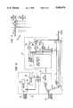
- FIG. 1is a block diagram of a computer system wherein a plurality of processors share a resource.
- FIG. 2is a block diagram of the address aliasing device of FIG. 1, according to the present invention.
- FIG. 3illustrates an address input to the address aliasing device of FIG. 2.
- FIG. 4illustrates a table summarizing information contained in the look-up table device of FIG. 2.
- the computer system 10comprises a plurality of processors 12, 14 and a resource module 16 coupled to one another by a backplane bus 18.
- the resource module 16includes a RAM 20 and an address aliasing device 22 according to the present invention.
- a point-to-point coupling 24is arranged to couple an output of the address aliasing device 22 to an address port of the RAM 20.
- the address aliasing device 22further includes a register arrangement 22A containing RAM section size information, as will be described below.
- a resource 26is coupled to address, data read and data write ports of the RAM 20 by a coupling 28.
- the resource 26can comprise a processor whose function includes the performance of a preselected processing service for any of the processors 12, 14.
- Each of the processors 12, 14 and the resource module 16is provided with a backplane bus interface 30A, 30B, 30C, respectively, to control communication over the backplane bus 18.
- the backplane bus 18 and backplane bus interfaces 30A, 30B, 30Ccan be operated according to the Futurebus asynchronous backplane bus protocol standard promulgated by the IEEE (ANSE/IEEE Std. 896.1).
- the bus interface 30Ccouples appropriate address lines from the bus 18 to an input of the address aliasing device 22 and appropriate data lines to the data read and data write ports of the RAM 20 via lines 32.
- a processor 12, 14When a processor 12, 14 requires the resource 26 for performance of the processing service, it will arbitrate for control of the backplane bus 18 through the respective backplane bus interface 30A, 30B and, upon obtaining control of the backplane bus 18, transmit an address for a predetermined location in the RAM 20.
- the processor 12, 14will first read the addressed location to verify ownership and then write a request for service and other relevant information into the location of the RAM 20 identified by the transmitted address when the processor 12, 14 owns the location.
- the resource 26operates to poll the RAM 20 for requests to process via the coupling 28.
- a management processor 34is also coupled to the bus 18 by a bus interface 36.
- a coupling 38couples the bus interface 30C to the register arrangement 22A of the resource module 16 so that the register arrangement 22A can be accessed via the bus 18, as for example, by the management processor 34 for writing of RAM section size information, as will be described.
- the address transmitted by the processor 12, 14 over the bus 18is input to the address aliasing device 22.
- the output of the address aliasing device 22comprises an alias of the input address which is input to the address port of the RAM 20 via the line 24, as will appear.
- the RAM 20is logically divided into a plurality of fixed size ring buffers which are each allocated to one of the processors 12, 14 for exclusive use in writing requests to the resource 26.
- the RAM 20comprises a 4K RAM divided into sixteen ring buffers of 256 bytes each.
- the illustration of processors 12, 14is representative only, as, for example, there can be a total of sixteen processors coupled to the bus 18 with each processor being allocated one of the sixteen 256 byte buffers as an interlock to the resource 26 and so on for different numbers of processors and ring buffers.
- the address aliasing device 22In the 4K RAM example, a 12 bit address is needed to uniquely identify one of the total of 4,096 addressable locations available in the RAM 20. Accordingly, the lines 32 from the bus interface 30C that are coupled to the input of the address aliasing device 22 comprise 12 bits of the address transmitted over the bus 18. As should be understood, the address transmitted by the processor 12, 14 is determined by the address space defined by the bus protocol. For example, a 32 bit address is utilized in the Futurebus protocol. The 12 bits utilized to address the 4K RAM 20 can comprise the 12 low order bits of the 32 bit bus address. These 12 bits are used by each processor 12, 14 to address one location in an allocated 256 byte section of the RAM 20 within the 32 bit bus address space.
- the four high order bits ⁇ 11:8>are input to a size selector device 52.
- the RAM section size register arrangement 22Acomprises two 16 bit registers 54A and 54B for a total of 32 bits of storage space. Accordingly, 16 two bit sections of the 32 bits are each dedicated as a two bit size selector for a corresponding one of the 16 ring buffer sections of the RAM 20 defined by bits ⁇ 11:8>.
- the 32 bits stored in the registers 54A, 54Bprovide a mask for setting the total number of addressable locations in each of the 16 sections of the RAM 20 that are to be used as a ring buffer by the respective processor 12, 14.
- the size selector device 52functions as a multiplexer receiving as an input all 32 bits stored in the registers 54A, 54B.
- the bits ⁇ 11:8> input to the size selector device 52are used as a multiplexer select control to select the one two-bit size selector of the 32 bits of the registers 54A, 54B that corresponds to the RAM section defined by bits ⁇ 11:8>.
- the selected two bit size selectoris output by the size selector device 52.
- the two bit size selector output of the size selector device 52is input as an index to a size selector decode look-up table 56.
- the look up tablecontains four locations, one for each possible value of the two bit size selector index input to the look-up table 56. Each location stores a three bit size code that is output by the look-up table 56.
- the three bit codescorrespond to bits ⁇ 7>, ⁇ 6> and ⁇ 5> of the 12 bit input address and represent full, half, quarter and eighth sizes for the corresponding RAM section defined by bits ⁇ 11:8>. More specifically, code 000 indicates that the full 256 bytes of the RAM section are available to store requests for the resource 26 by the respective processor 12, 14; code 100 indicates that half, or 128 bytes, of the RAM section are to be used for storing requests; code 110 indicates 64 bytes (one quarter of the section); and code 111 indicates 32 bytes (one eighth of the RAM section).
- bits ⁇ 4:0>will identify 32 unique locations within the RAM section indicated by bits ⁇ 11:8>.
- Bit ⁇ 5>identifies 64 unique locations, i.e. a logical 1 for bit ⁇ 5> with each of the 32 possible values for bits ⁇ 4:0> and a zero for bit ⁇ 5> with each of the 32 possible values for bits ⁇ 4:0>.
- a logical combination of the three bits output by the look-up table 56 with corresponding bits ⁇ 5:7> of the 12 bit input addressis utilized to alias the sequence of addresses output by the address aliasing device 22, as will now be described.
- a set of OR gates 60A, 60B, 60Ccorresponds to bits ⁇ 7:5> of the 12 bit input address.
- Each of the OR gates 60A, 60B, 60Ctakes as a first input a corresponding one of the bits of the three bit code output by the look-up table 56.
- the OR gate 60Atakes as a second input bit ⁇ 7> of the 12 bit input address
- the OR gate 60Btakes as a second input bit ⁇ 6> of the 12 bit input address
- the OR gate 60Ctakes a second input bit ⁇ 5> of the 12 bit input address.
- the 12 bit address output of the address aliasing device 22comprises bits ⁇ 4:0> of the 12 bit input address, the outputs of the OR gates 60A, 60B, 60C and bits ⁇ 11:8> of the 12 bit input address.
- the output of the OR gates 60A, 60B, 60Cwill be determined by the value of the bits ⁇ 7:5> of the 12 bit input address. This is because the three bit code provides three zeros as inputs to the OR gates 60A, 60B, 60C and the value of each of the OR gate outputs will be a zero when the corresponding bit ⁇ 7:5> from the 12 bit input address is zero and will be a logical 1 when the corresponding bit from the 12 bit input address is a logical 1.
- the processor 12, 14will control the values for bits ⁇ 7:5> and be able to specify one of 256 locations for full use of the respective RAM section defined by bits ⁇ 11:8> of the address.
- the input to the OR gate 60A from the output of the look-up table 56will be a logical 1 and, therefore, the output of the OR gate 60A will remain a logical 1 regardless of the value of bit ⁇ 7> in the 12 bit input address.
- the address output by the address aliasing device 22will be within a range of 128 locations.
- the processor 12, 14will continue to generate 12 bit addresses within a 256 byte address space, but when an address contains a zero in bit ⁇ 7> an alias address having bit ⁇ 7> set at logical 1 will be output by the address aliasing device 22 via the logical 1 output of the OR gate 60A.
- the size of the allocated ring bufferwill be half of the 256 locations in the RAM section defined by bits ⁇ 11:8>.
- the address aliasing device 22will input an alias address corresponding to the location of the first request. The ownership will still be with the resource 26 and the processor 12, 14 must wait before it writes any additional requests into the respective allocated ring buffer section within the RAM 20.
- Code values of 110 and 111will achieve similar address aliasing effects for buffer sizes of 64 and 32 bytes, respectively.
- Code value 110causes the output of the OR gates 60A, 60B to remain at logical 1 and code value 111 causes the output of all of the OR gates 60A, 60B, 60C to remain at logical 1 regardless of the values for bits ⁇ 7:6> or ⁇ 7:5>, respectively, generated by the processor 12, 14.
- the processors 12, 14continue to generate addresses on the basis of a 256 location address space and the address aliasing device 22 aliases the generated addresses so that the size of the respective ring buffer is fixed at a number of locations that is fair relative to other processors 12, 14.
- the management processor 34At system initialization time the management processor 34 generates, as a function of system configuration, the values for the 32 bits of the code representing the size of each of the ring buffer sections of the RAM 20 which is to be used for the current configuration.
- the management processor 34writes the 32 bit code into the register arrangement 22A via the bus 18 and coupling 38.
- the code value represented by the 32 bits stored in the register arrangement 22Acan be updated as desired when new processors are added to the system, provided that the sizes of the buffers not currently in use are the only ones changed.
Landscapes
- Engineering & Computer Science (AREA)
- Theoretical Computer Science (AREA)
- Physics & Mathematics (AREA)
- General Engineering & Computer Science (AREA)
- General Physics & Mathematics (AREA)
- Multi Processors (AREA)
Abstract
Description
Claims (17)
Priority Applications (1)
| Application Number | Priority Date | Filing Date | Title |
|---|---|---|---|
| US07/819,393US5404474A (en) | 1992-01-10 | 1992-01-10 | Apparatus and method for addressing a variable sized block of memory |
Applications Claiming Priority (1)
| Application Number | Priority Date | Filing Date | Title |
|---|---|---|---|
| US07/819,393US5404474A (en) | 1992-01-10 | 1992-01-10 | Apparatus and method for addressing a variable sized block of memory |
Publications (1)
| Publication Number | Publication Date |
|---|---|
| US5404474Atrue US5404474A (en) | 1995-04-04 |
Family
ID=25228029
Family Applications (1)
| Application Number | Title | Priority Date | Filing Date |
|---|---|---|---|
| US07/819,393Expired - LifetimeUS5404474A (en) | 1992-01-10 | 1992-01-10 | Apparatus and method for addressing a variable sized block of memory |
Country Status (1)
| Country | Link |
|---|---|
| US (1) | US5404474A (en) |
Cited By (24)
| Publication number | Priority date | Publication date | Assignee | Title |
|---|---|---|---|---|
| US5615140A (en)* | 1994-02-14 | 1997-03-25 | Matsushita Electric Industrial Co., Ltd. | Fixed-point arithmetic unit |
| US5699544A (en) | 1993-06-24 | 1997-12-16 | Discovision Associates | Method and apparatus for using a fixed width word for addressing variable width data |
| US5724537A (en) | 1994-03-24 | 1998-03-03 | Discovision Associates | Interface for connecting a bus to a random access memory using a two wire link |
| US5761464A (en)* | 1995-05-22 | 1998-06-02 | Emc Corporation | Prefetching variable length data |
| US5761741A (en) | 1994-03-24 | 1998-06-02 | Discovision Associates | Technique for addressing a partial word and concurrently providing a substitution field |
| US5835502A (en)* | 1996-06-28 | 1998-11-10 | International Business Machines Corporation | Method and apparatus for handling variable data word widths and array depths in a serial shared abist scheme |
| US5861894A (en) | 1993-06-24 | 1999-01-19 | Discovision Associates | Buffer manager |
| EP0837474A3 (en)* | 1996-10-17 | 1999-09-15 | STMicroelectronics S.r.l. | Memory cells matrix for a semiconductor integrated microcontroller |
| US6119213A (en)* | 1995-06-07 | 2000-09-12 | Discovision Associates | Method for addressing data having variable data width using a fixed number of bits for address and width defining fields |
| US6167459A (en)* | 1998-10-07 | 2000-12-26 | International Business Machines Corporation | System for reassigning alias addresses to an input/output device |
| US6170023B1 (en) | 1998-10-07 | 2001-01-02 | International Business Machines Corporation | System for accessing an input/output device using multiple addresses |
| US6185638B1 (en) | 1998-10-07 | 2001-02-06 | International Business Machines Corporation | Method and system for dynamically assigning addresses to an input/output device |
| US6202095B1 (en) | 1998-10-07 | 2001-03-13 | International Business Machines Corporation | Defining characteristics between processing systems |
| US6230216B1 (en)* | 1999-01-28 | 2001-05-08 | Vlsi Technology, Inc. | Method for eliminating dual address cycles in a peripheral component interconnect environment |
| US6301631B1 (en)* | 1999-01-28 | 2001-10-09 | Vlsi Technology, Inc. | Memory mapping method for eliminating dual address cycles in a peripheral component interconnect environment |
| US6505283B1 (en)* | 1998-10-06 | 2003-01-07 | Canon Kabushiki Kaisha | Efficient memory allocator utilizing a dual free-list structure |
| US6629119B1 (en)* | 1999-05-06 | 2003-09-30 | Industrial Technology Research Institute | Arithmetic device and method with low power consumption |
| US6718416B1 (en)* | 2000-08-21 | 2004-04-06 | Intel Corporation | Method and apparatus for removing and installing a computer system bus agent without powering down the computer system |
| USRE40423E1 (en) | 1996-07-29 | 2008-07-08 | Xilinx, Inc. | Multiport RAM with programmable data port configuration |
| US7802062B2 (en) | 2007-09-28 | 2010-09-21 | Microsoft Corporation | Non-blocking variable size recyclable buffer management |
| US20160292077A1 (en)* | 2015-03-30 | 2016-10-06 | Ca, Inc. | Low-latency lossy processing of machine data |
| US10133653B2 (en)* | 2012-02-23 | 2018-11-20 | Cadence Design Systems, Inc. | Recording and playback of trace and video log data for programs |
| US11436525B2 (en)* | 2017-12-01 | 2022-09-06 | Deepwave Digital, Inc. | Artificial intelligence radio transceiver |
| US20220376842A1 (en)* | 2019-11-08 | 2022-11-24 | Lenovo (Beijing) Ltd. | Apparatus and method of sidelink bsr reporting |
Citations (4)
| Publication number | Priority date | Publication date | Assignee | Title |
|---|---|---|---|---|
| US5093783A (en)* | 1984-08-02 | 1992-03-03 | Nec Corporation | Microcomputer register bank accessing |
| US5109334A (en)* | 1987-10-27 | 1992-04-28 | Sharp Kabushiki Kaisha | Memory management unit capable of expanding the offset part of the physical address |
| US5150471A (en)* | 1989-04-20 | 1992-09-22 | Ncr Corporation | Method and apparatus for offset register address accessing |
| US5210839A (en)* | 1990-12-21 | 1993-05-11 | Sun Microsystems, Inc. | Method and apparatus for providing a memory address from a computer instruction using a mask register |
- 1992
- 1992-01-10USUS07/819,393patent/US5404474A/ennot_activeExpired - Lifetime
Patent Citations (4)
| Publication number | Priority date | Publication date | Assignee | Title |
|---|---|---|---|---|
| US5093783A (en)* | 1984-08-02 | 1992-03-03 | Nec Corporation | Microcomputer register bank accessing |
| US5109334A (en)* | 1987-10-27 | 1992-04-28 | Sharp Kabushiki Kaisha | Memory management unit capable of expanding the offset part of the physical address |
| US5150471A (en)* | 1989-04-20 | 1992-09-22 | Ncr Corporation | Method and apparatus for offset register address accessing |
| US5210839A (en)* | 1990-12-21 | 1993-05-11 | Sun Microsystems, Inc. | Method and apparatus for providing a memory address from a computer instruction using a mask register |
Cited By (27)
| Publication number | Priority date | Publication date | Assignee | Title |
|---|---|---|---|---|
| US5861894A (en) | 1993-06-24 | 1999-01-19 | Discovision Associates | Buffer manager |
| US5699544A (en) | 1993-06-24 | 1997-12-16 | Discovision Associates | Method and apparatus for using a fixed width word for addressing variable width data |
| US5615140A (en)* | 1994-02-14 | 1997-03-25 | Matsushita Electric Industrial Co., Ltd. | Fixed-point arithmetic unit |
| US5724537A (en) | 1994-03-24 | 1998-03-03 | Discovision Associates | Interface for connecting a bus to a random access memory using a two wire link |
| US5761741A (en) | 1994-03-24 | 1998-06-02 | Discovision Associates | Technique for addressing a partial word and concurrently providing a substitution field |
| US5956741A (en) | 1994-03-24 | 1999-09-21 | Discovision Associates | Interface for connecting a bus to a random access memory using a swing buffer and a buffer manager |
| US5761464A (en)* | 1995-05-22 | 1998-06-02 | Emc Corporation | Prefetching variable length data |
| US6119213A (en)* | 1995-06-07 | 2000-09-12 | Discovision Associates | Method for addressing data having variable data width using a fixed number of bits for address and width defining fields |
| US5835502A (en)* | 1996-06-28 | 1998-11-10 | International Business Machines Corporation | Method and apparatus for handling variable data word widths and array depths in a serial shared abist scheme |
| USRE40423E1 (en) | 1996-07-29 | 2008-07-08 | Xilinx, Inc. | Multiport RAM with programmable data port configuration |
| EP0837474A3 (en)* | 1996-10-17 | 1999-09-15 | STMicroelectronics S.r.l. | Memory cells matrix for a semiconductor integrated microcontroller |
| US6122702A (en)* | 1996-10-17 | 2000-09-19 | Sgs-Thomson Microelectronics S.R.L. | Memory cells matrix for a semiconductor integrated microcontroller |
| US6505283B1 (en)* | 1998-10-06 | 2003-01-07 | Canon Kabushiki Kaisha | Efficient memory allocator utilizing a dual free-list structure |
| US6170023B1 (en) | 1998-10-07 | 2001-01-02 | International Business Machines Corporation | System for accessing an input/output device using multiple addresses |
| US6167459A (en)* | 1998-10-07 | 2000-12-26 | International Business Machines Corporation | System for reassigning alias addresses to an input/output device |
| US6202095B1 (en) | 1998-10-07 | 2001-03-13 | International Business Machines Corporation | Defining characteristics between processing systems |
| US6185638B1 (en) | 1998-10-07 | 2001-02-06 | International Business Machines Corporation | Method and system for dynamically assigning addresses to an input/output device |
| US6301631B1 (en)* | 1999-01-28 | 2001-10-09 | Vlsi Technology, Inc. | Memory mapping method for eliminating dual address cycles in a peripheral component interconnect environment |
| US6230216B1 (en)* | 1999-01-28 | 2001-05-08 | Vlsi Technology, Inc. | Method for eliminating dual address cycles in a peripheral component interconnect environment |
| US6629119B1 (en)* | 1999-05-06 | 2003-09-30 | Industrial Technology Research Institute | Arithmetic device and method with low power consumption |
| US6718416B1 (en)* | 2000-08-21 | 2004-04-06 | Intel Corporation | Method and apparatus for removing and installing a computer system bus agent without powering down the computer system |
| US7802062B2 (en) | 2007-09-28 | 2010-09-21 | Microsoft Corporation | Non-blocking variable size recyclable buffer management |
| US10133653B2 (en)* | 2012-02-23 | 2018-11-20 | Cadence Design Systems, Inc. | Recording and playback of trace and video log data for programs |
| US20160292077A1 (en)* | 2015-03-30 | 2016-10-06 | Ca, Inc. | Low-latency lossy processing of machine data |
| US11436525B2 (en)* | 2017-12-01 | 2022-09-06 | Deepwave Digital, Inc. | Artificial intelligence radio transceiver |
| US11790273B2 (en) | 2017-12-01 | 2023-10-17 | Deepwave Digital, Inc. | Artificial intelligence radio transceiver |
| US20220376842A1 (en)* | 2019-11-08 | 2022-11-24 | Lenovo (Beijing) Ltd. | Apparatus and method of sidelink bsr reporting |
Similar Documents
| Publication | Publication Date | Title |
|---|---|---|
| US5404474A (en) | Apparatus and method for addressing a variable sized block of memory | |
| US4933846A (en) | Network communications adapter with dual interleaved memory banks servicing multiple processors | |
| US6185654B1 (en) | Phantom resource memory address mapping system | |
| US6813653B2 (en) | Method and apparatus for implementing PCI DMA speculative prefetching in a message passing queue oriented bus system | |
| US4648035A (en) | Address conversion unit for multiprocessor system | |
| JP3687990B2 (en) | Memory access mechanism | |
| US5315708A (en) | Method and apparatus for transferring data through a staging memory | |
| US4814974A (en) | Programmable memory-based arbitration system for implementing fixed and flexible priority arrangements | |
| US7487505B2 (en) | Multithreaded microprocessor with register allocation based on number of active threads | |
| US5247629A (en) | Multiprocessor system with global data replication and two levels of address translation units | |
| US4485438A (en) | High transfer rate between multi-processor units | |
| US5261077A (en) | Configurable data path arrangement for resolving data type incompatibility | |
| US6189062B1 (en) | Apparatus and method for address translation in bus bridge devices | |
| US4695948A (en) | Bus to bus converter using a RAM for multiple address mapping | |
| JPH0792654B2 (en) | Video data frame transmission method and apparatus | |
| KR900002894B1 (en) | Data Processing System Using Address Translation | |
| EP0229932B1 (en) | High-capacity memory for multiprocessor systems | |
| US5548777A (en) | Interface control system for a CD-ROM driver by memory mapped I/O method having a predetermined base address using an ISA BUS standard | |
| US5446844A (en) | Peripheral memory interface controller as a cache for a large data processing system | |
| JPH0587854B2 (en) | ||
| US5428760A (en) | Circuitry and method for sharing internal microcontroller memory with an external processor | |
| WO1996035176A1 (en) | Bus bridge address translator | |
| CN1171577A (en) | Programmable read/write access signal and method therefor | |
| US4604709A (en) | Channel communicator | |
| JPH0581939B2 (en) |
Legal Events
| Date | Code | Title | Description |
|---|---|---|---|
| AS | Assignment | Owner name:DIGITAL EQUIPMENT CORPORATION, MASSACHUSETTS Free format text:ASSIGNMENT OF ASSIGNORS INTEREST.;ASSIGNORS:CROOK, NEAL A.;BRYANT, STEWART F.;REEL/FRAME:005982/0258 Effective date:19911212 Owner name:DIGITAL EQUIPMENT CORPORATION, MASSACHUSETTS Free format text:ASSIGNMENT OF ASSIGNORS INTEREST.;ASSIGNOR:LENTHALL, JOHN M.;REEL/FRAME:005982/0266 Effective date:19911218 | |
| AS | Assignment | Owner name:DIGITAL EQUIPMENT CORPORATION, MASSACHUSETTS Free format text:ASSIGNMENT OF ASSIGNORS INTEREST.;ASSIGNOR:SEAMAN, MICHAEL J.;REEL/FRAME:006238/0298 Effective date:19920803 | |
| STCF | Information on status: patent grant | Free format text:PATENTED CASE | |
| AS | Assignment | Owner name:CABLETRON SYSTEMS, INC., NEW HAMPSHIRE Free format text:ASSIGNMENT OF ASSIGNORS INTEREST;ASSIGNOR:DIGITAL EQUIPMENT CORPORATION;REEL/FRAME:009046/0792 Effective date:19980206 | |
| FPAY | Fee payment | Year of fee payment:4 | |
| AS | Assignment | Owner name:ENTERASYS NETWORKS, INC., NEW HAMPSHIRE Free format text:ASSIGNMENT OF ASSIGNORS INTEREST;ASSIGNOR:CABLETRON SYSTEMS, INC.;REEL/FRAME:011219/0376 Effective date:20000929 | |
| FEPP | Fee payment procedure | Free format text:PAYOR NUMBER ASSIGNED (ORIGINAL EVENT CODE: ASPN); ENTITY STATUS OF PATENT OWNER: LARGE ENTITY | |
| FPAY | Fee payment | Year of fee payment:8 | |
| AS | Assignment | Owner name:WELLS FARGO FOOTHILL, INC., CALIFORNIA Free format text:SECURITY AGREEMENT;ASSIGNOR:ENTERASYS NETWORKS, INC.;REEL/FRAME:017656/0552 Effective date:20060516 Owner name:OBSIDIAN, LLC, CALIFORNIA Free format text:SECURITY AGREEMENT;ASSIGNOR:ENTERASYS NETWORKS, INC.;REEL/FRAME:017656/0552 Effective date:20060516 | |
| FPAY | Fee payment | Year of fee payment:12 | |
| AS | Assignment | Owner name:WELLS FARGO TRUST CORPORATION LIMITED, AS SECURITY Free format text:GRANT OF SECURITY INTEREST IN U.S. PATENTS;ASSIGNOR:ENTERASYS NETWORKS INC.;REEL/FRAME:025339/0875 Effective date:20101109 | |
| AS | Assignment | Owner name:ENTERASYS NETWORKS, INC., MASSACHUSETTS Free format text:RELEASE AND REASSIGNMENT OF PATENTS AND PATENT APPLICATIONS AT REEL/FRAME NO. 17656/0552;ASSIGNORS:WELLS FARGO CAPITAL FINANCE, INC. (FORMERLY KNOWN AS WELLS FARGO FOOTHILL, INC.);ENTERPRISE COMMUNICATIONS FUNDING GMBH, AS SUCCESSOR IN INTEREST TO OBSIDIAN, LLC;REEL/FRAME:025406/0769 Effective date:20101110 |