US5404464A - Bus control system and method that selectively generate an early address strobe - Google Patents
Bus control system and method that selectively generate an early address strobeDownload PDFInfo
- Publication number
- US5404464A US5404464AUS08/016,726US1672693AUS5404464AUS 5404464 AUS5404464 AUS 5404464AUS 1672693 AUS1672693 AUS 1672693AUS 5404464 AUS5404464 AUS 5404464A
- Authority
- US
- United States
- Prior art keywords
- bus
- address
- data
- memory
- modules
- Prior art date
- Legal status (The legal status is an assumption and is not a legal conclusion. Google has not performed a legal analysis and makes no representation as to the accuracy of the status listed.)
- Expired - Lifetime
Links
Images


Classifications
- G—PHYSICS
- G06—COMPUTING OR CALCULATING; COUNTING
- G06F—ELECTRIC DIGITAL DATA PROCESSING
- G06F12/00—Accessing, addressing or allocating within memory systems or architectures
- G06F12/02—Addressing or allocation; Relocation
- G06F12/08—Addressing or allocation; Relocation in hierarchically structured memory systems, e.g. virtual memory systems
- G06F12/0802—Addressing of a memory level in which the access to the desired data or data block requires associative addressing means, e.g. caches
- G06F12/0806—Multiuser, multiprocessor or multiprocessing cache systems
- G06F12/0815—Cache consistency protocols
- G06F12/0831—Cache consistency protocols using a bus scheme, e.g. with bus monitoring or watching means
- G06F12/0833—Cache consistency protocols using a bus scheme, e.g. with bus monitoring or watching means in combination with broadcast means (e.g. for invalidation or updating)
- G—PHYSICS
- G06—COMPUTING OR CALCULATING; COUNTING
- G06F—ELECTRIC DIGITAL DATA PROCESSING
- G06F13/00—Interconnection of, or transfer of information or other signals between, memories, input/output devices or central processing units
- G06F13/14—Handling requests for interconnection or transfer
- G06F13/16—Handling requests for interconnection or transfer for access to memory bus
- G06F13/1605—Handling requests for interconnection or transfer for access to memory bus based on arbitration
- G06F13/1652—Handling requests for interconnection or transfer for access to memory bus based on arbitration in a multiprocessor architecture
- G06F13/1663—Access to shared memory
Definitions
- the present inventionrelates to an improved bus architecture which decreases the bus access time in a tightly coupled multi-processor system.
- bus latencyIn a tightly coupled multi-processor system, all of the processors in the system share a common address and data bus, as well as a common system memory.
- the busWhen a multi-processor system employs a single common bus for address and data transfers, the bus must be restricted to one transfer at a time. Therefore, when one processor is communicating with the memory, all other processors are either busy with their own internal operations or must be idle, waiting for the bus to become free. The time that the processor spends waiting idle for the bus to become available is referred to as bus latency.
- the address busis needed only for a short time while the addressed memory unit decodes the memory request. The correct memory board will then latch the address from the address bus. The address bus remains idle for the remainder of the data transfer. The data transfer time may be quite long depending upon the type of memory storage unit.
- Some multi-processor systemsuse a split transaction bus in order to cut down on the time that the bus is being held.
- the address and data busoperate independently, thus allowing multiple requests to be outstanding.
- the requestor of the busactivates an address request to the address bus.
- the addressed devicee.g., memory module
- the requestorreleases the address bus for other address requests.
- the deviceacquires the bus and delivers the data to the requestor.
- the address busis therefore available for other memory requests while the memory system delivers the requested data to the requestor.
- the split transaction bus methodreduces bus latency; however, the complexity of the system is increased dramatically.
- the memory boards for a split transaction systemrequire the ability to queue and possibly sort requests, and must be provided with bus controller capabilities.
- the queue capabilityrequires additional memory space to store and queue the outstanding requests and additional control logic to implement the bus controller.
- the amount of time that is saved between bus requestsmay decrease with increased bus transaction time.
- the memory access cycle time in a split transaction busis typically longer then in a single bus system because each cycle includes steps to perform the queuing and bus control functions. If the queuing and bus control steps take longer than the time saved between transaction, the benefits of the "time saving" split transaction bus can quickly diminish. Without the return of a substantial decrease in the overall system memory access time, the increase in the complexity of the system that is required to implement a split transaction bus is often not justified. Maintaining cache coherency further complicates the implementation of a split transaction bus architecture.
- the present inventionis an improved bus architecture system for use in a tightly-coupled multi-processor system with memory storage separated into separate memory modules.
- the design of the present inventionmakes use of unused bus time and does not introduce complexities into the system which reduce the overall bandwidth increase.
- the improved bus architecture of the present inventionutilizes memory mapping, wherein the memory is mapped across several separate memory boards.
- the systemprovides concurrent outstanding address requests on the bus if these requests are for accesses to memory locations located on separate memory modules.
- the present inventiondecreases bus latency when any equivalent bus requests involve accesses to data from separate memory modules.
- the improved bus control system of the present inventionis preferably utilized in a multi-processor system having at least two memory modules, and having a common address and data bus connecting the memory modules to the processor modules.
- a preferred embodiment of the improved bus control systemincludes means for determining a first slot identifier of a first one of the memory modules which contains a first data request and means for storing the first slot identifier.
- the bus control systemincludes means for determining a second slot identifier for a second memory address request and means for comparing the first slot identifier with the second slot identifier.
- a static random access memory (SRAM)is used to determine the first and second slot identifiers, and a storage register is used to store the first slot identifier.
- a comparatoris used to compare the first and second slot identifiers. If the first slot identifier differs from the second slot identifier, a means for issuing an early address request to the common bus is provided. Preferably, a simple logic circuit is used to issue an early address request to the common bus. Further, the preferred embodiment of the improved bus control system includes means for disabling the issuance of the early address request by any one of the processor modules if the feature is not desired.
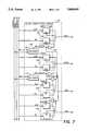
- FIG. 1is a system block diagram of a multi-processor system which implements the bus architecture of the present invention.
- FIG. 2is a block diagram representing an individual CPU module and its communication channels with the address and data bus.
- FIG. 3is a timing diagram illustrating the normal read cycle for a snoop-miss data request on a multi-processor system without the bus architecture of the present invention.
- FIG. 4is a block diagram of one embodiment of the circuitry to implement the bus architecture of the present invention.
- FIG. 5is a timing diagram of the improved access time of a snoop-miss data request utilizing the bus architecture of the present invention.
- FIG. 6illustrates an example of a preferred cache line interleaving scheme employed in a system memory.
- FIG. 7is a block diagram of an address line exchange circuit according to the present invention.
- FIG. 8is a block diagram illustrating a memory addressing circuit to realize an interleaved memory mapping technique.
- FIG. 1illustrates a conventional multi-processor system 10 which contains a number of CPU modules 12 (i.e., CPU MODULE #1, CPU MODULE #2, ... CPU MODULE #L) and a shared memory storage area containing a number of memory modules 14 (i.e., MEMORY MODULE #1, MEMORY MODULE #2, ... MEMORY MODULE #M).
- the CPU modules 12 and memory modules 14are connected to a system address bus 16, a system data bus 18 and a system control bus 20 (collectively the "system bus" 22).
- the multi-processor system 10may also include various I/O and peripheral modules (i.e., MISC I/O #1, MISC I/O #2...MISC I/O #N) 24 which are connected together along an I/O bus 26.
- a peripheral system controller or I/O service module (IOSM Module) 28provides an interface between the system bus 22 and the I/O bus 26 to control the data flow between the peripheral devices 24 and the system bus 22.
- each memory module 14comprises a plurality of random access memory (RAM) chips organized on a circuit board with accompanying decoder logic to read and decode the address requests.
- RAMrandom access memory
- the storage capacity of each memory module 14depends upon the number of RAM chips that are installed on the circuit board and the capacity of each RAM chip, as is well known in the art.
- the system memory addressesare divided among the individual memory modules 14 based upon the memory capacity of each module 14.
- the memory mapis generated on power-up by the system basic input/output system (BIOS).
- BIOSsystem basic input/output system
- FIG. 2illustrates a block diagram of a typical CPU module 12 used in the multi-processor system 10 of FIG. 1.
- the CPU module 12comprises a microprocessor 30, a cache memory system ("CACHE") 32 with internal address decoder logic, a CPU or local processor bus 34, bus transceivers 35 and system bus controller logic 36.
- CACHEcache memory system
- each CPU module 12further has a bandwidth maximizer circuit 38.
- the CPU modules 12 of the multi-processor system 10utilize a typical snooping cache, as is well known in the art.
- each cache 32monitors the address to determine if the cache 32 contains the requested data.
- the bus transceivers 35 of each CPU module 12read each address request from the system address bus 16. The address is transmitted via a local processor bus 34 to the cache 32 on the CPU module 12. If the cache 32 has the data for the requested address, a signal is sent to the system bus 22, commonly known as a snoop hit signal.
- the system data bus 18is available, the data is provided from the CPU cache 32 which detected a snoop hit to the data bus 18, as is well known in the art.
- FIG. 3illustrates a read cycle of a CPU module 12 of a multi-processor system 10 for a memory cycle with a snoop miss (i.e., the requested data was not in a cache 32).
- a CPU1initiates a BUSREQUEST signal (not shown) to a system bus arbitrator. When the system data bus 18 is available, the bus arbitrator returns a BUSGRANT signal (not shown) to the CPU1.
- the cycle timing of FIG. 3begins after the BUSGRANT signal. As illustrated in FIG. 3, once the CPU1 receives the BUSGRANT signal, the CPU1 holds the system address bus 16 in a first clock cycle by driving the address bus available line (ABUSAVL) 40 low.
- ABSVLaddress bus available line
- the system address from CPU1is presented to the system address bus 16 via the SADDRxx lines 42.
- the CPU1asserts the system address strobe, SADDS- line 44, in the second clock cycle.
- the addressis valid from clock cycle 2 through clock cycle 5.
- the devices which latch the addressdo so in response to the signal of the SADDS- signal line 44.
- the memory modules 14 and the CPU caches 32then determine if they contain the requested data. While each CPU cache 32 and memory module 14 determines if it has the requested data, each CPU module 12 and memory module 14 drives the transaction hold (TRNSHLD-) signal 46 low. In other words, initially, several devices may be driving the TRNSHLD- line 46 low. Therefore, until the last device releases the TRNSHLD- line 46, the line 46 remains low.
- the system bus busy line (SBUSBSY-) 48is also driven low by the CPU1 to indicate that a cache 32 transfer is in process.
- Each CPU cache 32 and memory module 14releases the transaction hold, or TRNSHLD-, signal line 46 when it determines that it does not contain the requested data. Therefore, the read cycle remains on hold until all of the memory storage areas check for the requested data. The last device to release the TRNSHLD- signal 46 will be assumed to contain the requested data. In the example of FIG. 3, the TRNSHLD- signal 46 is held low from clock cycle 3 to clock cycle 5, and the last memory storage device to release the TRNSHLD- signal line 46 is, for purposes of this example, memory module 1.
- memory module 1drives the CTERM- line 50 low during clock cycle 8.
- the valid datais presented to the system data bus 18 on lines SMD[63:00]51, and is valid from clock cycle 8 through clock cycle 11.
- the SEOT- line 52is strobed low at clock cycle 12, and the CTERM- line 50 returns to a normal high level.
- the system address bus busy line, SBUSBSY- line 48returns high, indicating availability of the system bus 22 for further requests.
- CPU2makes an address request by driving the ABUSAVL line 40 low, asserting the desired address on the system address lines, SADDRxx 42, and strobing the address bus request line, SADDS- 44.
- the CPU2drives the ABUSAVL line 40 low, signalling that the system address bus 16 is busy with a new request.
- the read cyclerepeats for the read request of CPU2.
- the system address bus 16is not used from clock cycle 7 into clock cycle 11, yet the system address bus 16 is held "busy" as part of the system bus 22. This prevents another CPU module 12 from issuing a bus request and starting a new cycle. Similarly, during the interval from clock cycle 18 into clock cycle 22, the system address bus 16 is not in use. As described below, the bandwidth maximizer circuit 38 utilizes these unused intervals in a typical read cycle when the system address bus 16 is not in use but the read cycle has not been completed. In general, the bandwidth maximizer circuit 38 allows a second bus master device such as a CPU 12 to issue an early address request without interfering with an address request already in progress.
- FIG. 4illustrates a block diagram of the bandwidth maximizer circuit 38 of the present invention.
- the preferred embodiment of the bandwidth maximizer circuit 38comprises an A5/A6 address line substitution circuit 54, a multiplexer (MUX) 56, a memory mapped decoder 58, a slot I.D. mapping static random access memory 60, a Last Slot I.D. register 62, a Slot Comparator 64, a NOR gate 66 and an AND gate 68.
- the bandwidth maximizer circuit 38is coupled to the local system bus 34 comprising a local address bus 70, the local data bus 72, the local control bus 74 and the bus controller 36 on the CPU module 12.
- the slot I.D. mapping SRAM 60is organized as 4,096 (4K) words by 5 bits per word.
- the slot I.D. mapping SRAM 60stores the memory map information which is configured at power-up by the system bios. More particularly, the first four bits of each location in the slot I.D. mapping SRAM 60 store the slot number of the memory module 14 assigned to the address range in system memory mapped by each location in the slot I.D. mapping SRAM 60.
- the fifth bit of each location in the slot I.D. mapping SRAM 60is assigned as a slot overlap disable flag for the memory range mapped by each location in the slot I.D. mapping SRAM 60.
- the bus controller 36 on the CPU module 12controls the communications between each CPU module 12 and the system bus 22.
- the MUX 56either selects address lines A2-A13 76 or A20-A31 78 from the local address bus 70 and provides them to the slot I.D. mapping SRAM 60.
- the decoder 58is responsive to write operations to the addresses assigned to the slot I.D. mapping SRAM 60 to activate an output connected to the MUX 56, and thereby cause the MUX 56 to select address lines A2-A13 76 for coupling to the outputs of the MUX 56.
- the outputs of the MUX 56are coupled to the address inputs of the slot I.D. mapping SRAM 60.
- the decoder 58is also responsive to the addresses assigned to the slot I.D.
- mapping SRAM 60to enable an output connected to the write enable (WE) input 80 of the slot I.D. mapping SRAM 60. Therefore, when the decoder 58 detects that the address request is to an address assigned to the slot I.D. mapping SRAM 60, the decoder 58 connects address lines A2-A13 76 to the address inputs of the slot I.D. mapping SRAM 60, and simultaneously activates the write enable input 80 to the slot I.D. mapping SRAM 60, allowing the SRAM 60 contents to be altered by storing the least significant 5 bits of data from the local data bus 72 via a set of data input lines 81. Write and read operations to addresses other than the addresses assigned to the slot I.D. mapping SRAM 60 do not activate the output of the decoder 58.
- the MUX 56selects address lines A20-A31 78 for coupling to its outputs, and in turn to the inputs to the slot I.D. mapping SRAM 60.
- the computer operating systemDuring initialization of the slot I.D. mapping SRAM 60, the computer operating system writes to the addresses assigned to the slot I.D. mapping SRAM 60.
- the decoder 58selects address lines A2-A13 76 for connection to the address inputs of the slot I.D. mapping SRAM 60.
- the system memoryis divided into blocks of 1 megabyte each.
- the slot numbers stored in each location of the slot I.D. mapping SRAM 60are assigned on the basis of the 1-megabyte divisions of memory.
- the computer operating systemstores the identifier "3" (011 in binary) in the first location of the slot I.D. mapping SRAM 60, and the identifier "4" (100 in binary) in the second location of the slot I.D. mapping SRAM 60.
- the decoder 58selects address lines A20-A31 78 for transmission through the mux 56 for connection to the address inputs of the slot I.D. mapping SRAM 60. Because A20 becomes the least significant bit of the address inputs to the slot I.D. mapping SRAM 60, the address to the slot I.D. mapping SRAM 60 only increments with each megabyte increment.
- the high throughput of the bandwidth maximizer circuit 38is achieved as long as the sequential address requests are to different memory modules (slots).
- the benefits of the bandwidth maximizer circuit 38are well achieved with at least two memory modules.
- the memoryis advantageously mapped so that sequential cache lines (32 bytes in the present embodiment) are fetched from different memory modules.
- address line A5is exchanged with address line A20 such that each 32-byte cache line is interleaved between two memory modules 14.
- address line A6is further exchanged with address line A21. This leads to each sequential 32-byte cache line being interleaved between four memory modules.
- An A5/A6 substitution circuit 54performs this function.
- An embodiment of an A5/A6 substitution circuit 54is depicted in detail in FIG. 7, and will be described in further below.
- each CPU module 12has an associated snooping cache
- all nonparticipating processors 30monitor (snoop) the address to maintain cache coherency, as is well known in the art.
- each processor 30latches each address from the system address bus 16 onto the local address bus 70 for comparison by the cache 32. Therefore, with each address request on the system address bus 16, the same address is present on the local address bus 70 for each CPU module 12 or other bus master module with a snooping cache in the system.
- Each cache 32determines if it has the requested data, as is well known in the art.
- the bandwidth maximizer circuit 38utilizes each address while it is active on the local address bus 70.
- each bandwidth maximizer circuit 38stores the slot I.D. of each address request in the Last Slot I.D. register 62.
- the Last Slot I.D. register 62 for each bandwidth maximizer circuit 38contains the slot I.D. of the last address request.
- the initiating CPU 12first places the address on its local address bus 70, and the bandwidth maximizer circuit 38 for that CPU 12 compares the slot I.D. for the new address with the slot I.D. of the last address. If the slot I.D. of the last request and the new request are to different slots, then the bandwidth maximizer circuit 38 for the requesting CPU issues an early address request during the period of the previous bus cycle in which the system address bus 16 is not used.
- the mux 56couples address lines A20-A31 78 to the address inputs of the Slot I.D. Mapping SRAM 60. Accordingly, the address on the local address bus 70 indexes the Slot I.D. Mapping SRAM 60.
- the slot I.D.i.e., slot number
- the mux 56couples address lines A20-A31 78 to the address inputs of the Slot I.D. Mapping SRAM 60. Accordingly, the address on the local address bus 70 indexes the Slot I.D. Mapping SRAM 60.
- the slot I.D.i.e., slot number
- the memory module 14corresponding to the address becomes active on four of the outputs to the SRAM 60. These four outputs are coupled to the Last Slot I.D. Register 62 and to the Slot Comparator 64.
- the outputs of the Last Slot I.D. Register 62are also coupled to the Slot Comparator 64. Until the current slot I.D. is clocked into the Last Slot I.D. Register 62, the outputs of the Last Slot I.D. Register 62 will contain signals representing the slot I.D. for the last address request. Therefore, before this clocking occurs, the Slot Comparator 64 compares the slot I.D. of the last address request to the slot I.D. of the current request.
- the clock signal for the Last Slot registeris the system address bus strobe, SADDS- line 44.
- the initiating CPUdoes not issue a strobe on the SADDS- signal line 44 until it enables the address on the system address bus 16. Therefore, until the initiating CPU issues a strobe on the SADDS- signal line 44, the slot I.D. of the present request will become available on the outputs of the Slot I.D. Mapping SRAM 60, and the outputs of the Last Slot I.D. register 62 will represent the slot I.D. of the previous address request on the system address bus 16.
- the comparator 64compares these slot I.D.s for equality. After the comparison, the slot I.D. of the new address request will be clocked into the Last Slot I.D Register 62 for the next time when the initiating processor 30 strobes the SADDS- signal line 44. This timing is illustrated in the upper portion of FIG. 5.
- the output of the Slot Comparator 64is one input to the NOR gate 66. If the last and current slot I.D.s are not equal, then the Slot Comparator 64 will not activate its output.
- the other input to the NOR gate 66is a Slot Overlap Disable signal line 81 which is the fifth output of the 5-bit wide Slot I.D. Mapping SRAM 60.
- the fifth bit of each memory location in the SRAM 60is a flag which can be set by the CPU to override (i.e., inhibit) the issuance of an early address request. For example, if a first CPU module 12 requests data directly from a second CPU module 12, it would not be advantageous to use the early address request function because the requested data is not found on one of the memory modules 14.
- the bandwidth maximizer circuit 38determines whether the system address bus 16 is available. The availability of the system address bus 16 is indicated by the ABUSAVL signal line 40.
- the AND gate 68having as inputs the ABUSAVL signal line 40 and the Enable Early Address signal line 82, determines whether the ABUSAVL signal line 40 is active while the Enable Early Address signal line 82 is active. If this condition exists, the output of the AND gate 68 (an Issue Early SADDS- signal line 84) becomes active to indicate to the bus controller 36 that an early SADDS- 44 may be issued by the issuing CPU module 14.
- the CPU bus controller 36may issue an early address request for the new data while the system bus 22 is still busy completing the last request. If the memory module 14 of the new request is the same as the memory module 14 of the current request, the requesting CPU 12 is caused to wait until the current memory cycle is completed before issuing the SADDS- 44.
- FIG. 5is a timing diagram of the system of the present invention for sequential snoop miss read operations, (i.e., the requested data is not located in any of the caches 32). This diagram illustrates the bandwidth increase which can occur by utilizing the bandwidth maximizer circuit 38 of the present invention.
- the initial portion of the read cycletracks the timing diagram of FIG. 3.
- the CPU1drives the ABUSAVL signal line 40 low, to indicate that the system address bus 16 is in use.
- CPU1enables the address onto the SADDRxx lines 42, and drives the system address bus line, SADDS- 44, low.
- SADDS- 44strobe, CPU1 drives the system address bus busy line (SBUSBSY- line 48), low starting during clock cycle 3.
- the memory modules 14 and the CPU cache storage areas 32check for the requested data and drive the transaction hold, TRNSHLD-, signal line 46 low.
- Each of the memory modules 14 and the CPU caches 32release the TRNSHLD- signal line 46 as each determines that it does not have the requested data. However, as long as any single module is still driving the TRNSHLD- signal line 46 low, this line remains low. During clock cycle 5, all of the memory modules 14 have released the TRNSHLD- signal line 46. In this example, it is assumed that memory module 1 contains the requested data.
- the CPU1releases the ABUSAVL signal line 40 in clock cycle 6.
- This sequenceindicates that the address on the system address bus 16 has been accepted and the address bus 16 is now available. However, the CPU1 continues to hold the SBUSBSY- signal line 48 active (low) until it receives the requested data. In the conventional systems described above, the system address bus 16 will remain unused until the cycle is complete.
- the bandwidth maximizer circuit 38 of the present inventionprovides for utilization of the system address bus 16 before the pending bus cycle is complete, as further described below.
- the upper portion of the timing diagram of FIG. 5illustrates the timing in the bandwidth maximizer circuit 38 of CPU2.
- the other CPUs in the systemalso track this timing.
- CPU2determines that the slot I.D. of the address request is the slot number for memory module 1.
- Thisis illustrated in the Slot RAM line 86 of the timing diagram which symbolizes the data at the outputs of the Slot I.D. Mapping SRAM 60.
- the SADDS- line 44returning high clocks the slot I.D. of the memory module of the data request into the Last Slot I.D. register 62 on each CPU module 12. This is illustrated in the Last Slot Reg line 88 of the timing diagram.
- CPU2has an address request ready. Therefore, CPU2 places the address on its local address bus 70. This address (i.e., the portion on address lines A20-A31) indexes the Slot I.D. Mapping SRAM 60 of the bandwidth maximizer circuit 38 for the CPU2. The four outputs of the Slot I.D. Mapping SRAM 60 for the CPU2 become active with the slot I.D. of the memory module 14 for the address request of the CPU2. The outputs of the Last Slot I.D. Register 62 are still active with the slot I.D. for the last address request by the CPU1. The comparator 64 compares the new slot I.D. with the last slot I.D.
- the comparator 64does not detect equality. This is represented in the Compare Results line 90 which is an active high signal when the two inputs to the comparator 64 are equal and is located on the upper portion of the timing diagram of FIG. 5. The timing diagram indicates the Compare Results line 90 will be inactive or low during clock cycles 7 and 8 as the two address requests are located on different memory modules 14.
- the bandwidth maximizer circuit 38also determines that the slot overlap disable bit has not been set with the NOR gate 66. For purposes of this description, it is assumed that the slot overlap disable bit stored in the fifth bit of the location in the Slot I.D. Mapping SRAM 60 corresponding to the address request of CPU2 is not set. Accordingly, the output of the NOR gate 66 becomes high.
- the bandwidth maximizer circuit 38 for the CPU2determines if the system address bus 16 is available (i.e., whether the ABUSAVL signal line 40 is high).
- the ABUSAVL signal line 40 in the lower portion of FIG. 5indicates that the ABUSAVL line 40 is high during clock cycle 7. Therefore, the output of the AND gate 68 becomes high. This indicates to the bus controller 36 for the CPU2 that it may place the address for the request of CPU2 on the system address bus 16 and issue a system address strobe.
- the CPU2drives the ABUSAVL line 40 low to take control of the system address bus 16.
- the bus controller 36 for the CPU2enables the new address onto the system address bus, SADDRxx lines 42, and strobes the SADDS- signal line 44 to indicate that the address is valid.
- each cache 32 and each memory module 14latch the address on the system address bus 16 and use this address to maintain cache coherency and to index the Slot I.D. Mapping SRAM 60.
- the strobe on the SADDS- line 44latches the four outputs of the Slot I.D. Mapping SRAM 60 into the Last Slot I.D. Register 62. This is represented in the Last Slot Reg line 88 of the upper portion of FIG. 5.
- the SADDS- line 44is active, the slot I.D. for memory module 2 is latched into the Last Slot I.D. Register 62.
- the CPU1When the CPU1 has accepted the data transfer, the CPU1 drives the CTERM- line 50 high, and the system end of transaction SEOT- signal line 52 is strobed low. Once both of these signals have occurred at clock cycle 12, the SBUSBSY- signal line 48 returns high because the read cycle for CPU1 is complete.
- the memory modules 14 and CPU cache memory storage areas 32determine if they contain the requested data for the second address request from the CPU2. While the memory modules 14 and cache memory storage areas 32 make this determination, they each drive the TRNSHLD- signal line 46 low. As explained above, it was assumed for the present description that the memory module 2 contains the data for address request of the CPU2. During clock cycle 13, the transaction hold line, TRNSHLD- 46, returns high to signal that a memory module 14 has the data requested by CPU2.
- the memory module 2drives the CTERM- signal line 50 low and enables the valid data on the data bus lines SMD[63:00]51. Simultaneously, the ABUSAVL line 40 returns high as the address of memory module 2 is no longer needed, and the SBUSBSY- line 48 will be pulled low to signal that the system data bus 18 will now be busy transmitting the data to CPU2. During clock cycles 14 through 17, the requested data from memory module 2 is available in the system data bus 18 at signal lines SMD[63:00]51, the CPU2 accepts the data and completes the second read cycle.
- the system address bus 16is available for another early data access, and if a new address request is for data stored on a different memory module 14 than the current memory module 14 (i.e., memory module 2), that request may proceed. For instance, if the CPU3 (or CPU1) now requests data from memory module 1 or memory module 3, at clock cycle 16, the CPU3 initiates a new memory address request for the new address, and the read cycle is once again initiated.
- the bandwidth maximizer circuit 38provides for the early issuance of an address request before the system bus read cycle for the previous request has completed. Providing for this early address request can provide an increase of over 50% in usable system bus bandwidth.
- sequential cache linesare preferably mapped to different memory modules 14 to increase the chances that two sequential memory accesses are for memory locations on different memory modules 14.
- FIG. 6illustrates the interleaving of cache lines between two memory modules 14.
- the linesare interleaved such that cache line n and all even additions to cache line n, i.e., n, n+2, n+4, etc., are located on the same memory module, and all odd additions to cache line n, i.e., n+1, n+3, n+5, etc., all appear on the second memory module.
- sequential memory addressesi.e., n and n+1, or n+1 and n+2 appear on different memory modules 14.
- one memory lineis interleaved, which increases the chances that sequential accesses will occur on different boards to 50% per board. If there are four memory modules 14, preferably, two memory lines are interleaved, which increases the chances that sequential accesses will occur on different boards.
- FIG. 7illustrates an example of a circuit which implements the substitution of two lower order bits, A5 and A6, with two higher order bits, A20 and A21.
- This circuitis advantageous for a system with at least four memory modules 14.
- the address line substitution circuitadvantageously substitutes address line A5 with address line A20.
- a first embodiment 54 of the A5/A6 substitution circuit that is required in FIG. 4is a slightly simpler embodiment, as it only requires two multiplexers, and will therefore be described last.
- a second embodiment of the A5/A6 substitution circuit 91is illustrated in FIG. 7 has four substitution multiplexers and is described below.
- a first multiplexer 92which comprises two enable gates or latches 94, 96 and a first memory mapped decoder 98 (which is shared by another multiplexer), the output of which is directly connected to the enable input of the first latch 94 and connected to the enable input of the second latch 96 through an inverter 100.
- the remaining three multiplexerscomprise a similar configuration.
- the input to the first latch 94 in the first multiplexer 92is the system address bus line A21
- the input to the second latch 96 in the first multiplexer 92is the system address line A6.
- the output of each latchis connected to the RAM address or memory address input line SA21 of the memory storage area.
- the first memory mapped decoder 98is connected to the system address bus 16 and the system control bus 18. The first memory mapped decoder 98 responds to a write operation to a predetermined address which has been assigned to the first decoder 98 to activate its output on an A6 select signal line 100.
- the A6 select signal line 100is connected to the enable input of the second latch 96 which has the address line A6 as an input, and is connected through an inverter 102 to the enable input of the first latch 94 which has the address line A21 as an input. Accordingly, when the A6 select signal line 100 becomes active, it selects the address line A6 for propagation through the latch and transmission to the SA21 address line of the memory storage area. In this manner, the A6 address line from the system address bus 16 is substituted for the A21 address line.
- the A6 select signal line 100becomes active when the first decoder 98 detects a write operation to a predetermined address. The first decoder 98 is also responsive to a second predetermined address to deactivate the A6 select line 100.
- the first multiplexer 92 which substitutes the A21 line for the RAM address input SA6is controlled via the same decoder 98 as the third multiplexer 104 which substitutes the A6 address line for the memory input SA21.
- the remaining two multiplexers 106, 108operate in a similar manner, but substitute address line A5 for address line A20, and address line A20 for address line A5, as controlled by the second decoder 110.
- the second decoder 110responds to first and second predetermined addresses to either select substitution or allow normal transmission. By providing substitution of only the A5/A20 combination, each subsequent 32-byte cache line will be mapped alternatively between two memory modules 14. By substituting both the A5/A20 and A6/A21 address lines, each subsequent 32-byte cache line is interleaved between four memory modules 14.
- the first embodiment of the A5/A6 substitution circuit 54only requires two multiplexers. When each cache line is interleaved, the address line substitutions are also provided to the upper address lines, A20-A31 78 in the present invention, of the multiplexer 56 in the bandwidth maximizer circuit 38 for each CPU module 12. However, since the lower address lines, A0-A19 are not used by the bandwidth maximizer circuit 38 during system memory accesses in the embodiment described above, address lines A21 and A20 need not be substituted for address lines A5 and A6. Thus, the first embodiment of the A5/A6 substitution circuit 54 for each bandwidth maximizer circuit 38 can be simplified by only providing two multiplexers to substitute address lines A5 and A6 for address lines A20 and A21, respectively.
- the first embodiment of the A5/A6 substitution circuit 54only requires the first multiplexer 92, the second multiplexer 106, the two decoders 98 and 110 and their respective connections, as illustrated in FIG. 7, to achieve the outputs SA20 and SA21.
- FIG. 8illustrates a block diagram of a preferred memory scheme for the multi-processor system 10 which is installed on the memory modules 14 of the system.
- the memory storage areawould typically be mapped into fairly large blocks of data (e.g., 1 megabyte in the embodiment described above).
- the lower memory address lines A0-A19need not be used to determine which memory module 14 is addressed by an address request.
- the cacheability/select mapping SRAM 112comprises 4-bit wide memory locations. In the present embodiment, three of the four bits are utilized for cacheability control. For each memory division or block of addresses (i.e., 1-megabyte address blocks in the present embodiment), that memory block is designated to have certain features with respect to the cache 32. These features include whether or not the locations are designated as cacheable memory locations, whether or not they are write-through locations, and whether or not they are memory-read-only locations. Therefore, three of the four bits in each memory location of the cacheability/select mapping SRAM 112 are utilized to store flags as to these three attributes of each block of memory. The fourth bit indicates whether the block of memory indexed by the location in which the bit is stored is located on the corresponding memory module 14.
- the fourth bit of the first location of the cacheability/select mapping SRAM 112 for the memory module 14 in slot 2will be set to indicate that block of memory addresses is assigned to the corresponding memory module 14.
- the fourth bitis advantageously connected to the memory select line of the memory storage area for the corresponding memory module 14.
- the cacheability/select mapping SRAM 112has 12 address inputs in the present embodiment, which are sufficient to index the 4K of memory locations of the cacheability/select mapping SRAM 112.
- the selection of which 12 lines are coupled to the cacheability/select mapping SRAM 112is controlled via a multiplexer (MUX) 114.
- the alternate inputs to the MUX 114are address lines A2-A14 and address lines A20-A31 78.
- the MUX 114selects either address lines A2-A14 or address lines A20-A31 78 for coupling to the input of the cacheability/select mapping SRAM 112.
- a memory mapped decoder 116responds to addresses assigned to the cacheability/select mapping SRAM 112 during initialization of the cacheability/select mapping SRAM 112 in order to select address lines A2-A14 for coupling to the SRAM 112.
- the decoder 116also activates an output connected to the write enable input (WE) 118 of the cacheability/select mapping SRAM 112 when the decoder 116 detects addresses assigned to the SRAM 112. Accordingly, during system initialization of the cacheability/select mapping SRAM 112, address lines A2-A14 are coupled to the SRAM 112, and the data representing the cacheability concerns and the memory map for the corresponding memory modules 14 are stored in the SRAM 112.
- the decoder 116detects that the address requests are to system memory address locations and selects address lines A20-A31 78 for coupling through the MUX 114 to the cacheability/select mapping SRAM 112. In this manner, as explained above, the cacheability/select mapping SRAM 112 is indexed by address lines A20-A31 78, which results in an increment to the address of the SRAM 112 with each subsequent increment in 1-megabyte memory blocks.
- the first embodiment of the A5/A6 substitution circuit 54substitutes A5 for address line A20, and A6 for address line A21 for inputs to the MUX 114 and the second embodiment of the A5/A6 substitution circuit 91 is used to substitute the addresses lines which go to the memory storage area. Accordingly, sequential 32-byte cache lines are fetched from different memory modules 14.
- the memoryis divided into increments of 8-megabyte memory blocks.
- the 8-megabyte memory block incrementis preferred when 8-megabyte SIMMS are used on the memory modules 14.
- the interleaved address linesare changed from A21 and A20 to A24 and A23, respectively.
- the system of the present inventionis advantageous over other bus systems as it enables a second CPU module 12 to begin a memory access before a first CPU module 12 has completed a memory request when the requests from the two CPU modules 12 access different memory modules 14.
- the typical system bus 22 for a multi-processor system 10has a large span of unused bus time while the current CPU 12 is holding the system bus 22 to prevent another CPU 12 from beginning a request.
- the bandwidth maximizer circuit 38 of the present inventiontakes advantage of the unused time. As long as the new address request is for a different memory module 14 than the previous request, a new request can be initiated prior to completion of the previous cycle.
- This elegant control systemcan increase bus bandwidth by over 50% if sequential memory requests are on different memory modules 14, and if the request is a cache snoop miss.
Landscapes
- Engineering & Computer Science (AREA)
- Theoretical Computer Science (AREA)
- Physics & Mathematics (AREA)
- General Engineering & Computer Science (AREA)
- General Physics & Mathematics (AREA)
- Memory System Of A Hierarchy Structure (AREA)
Abstract
Description
Claims (7)
Priority Applications (1)
| Application Number | Priority Date | Filing Date | Title |
|---|---|---|---|
| US08/016,726US5404464A (en) | 1993-02-11 | 1993-02-11 | Bus control system and method that selectively generate an early address strobe |
Applications Claiming Priority (1)
| Application Number | Priority Date | Filing Date | Title |
|---|---|---|---|
| US08/016,726US5404464A (en) | 1993-02-11 | 1993-02-11 | Bus control system and method that selectively generate an early address strobe |
Publications (1)
| Publication Number | Publication Date |
|---|---|
| US5404464Atrue US5404464A (en) | 1995-04-04 |
Family
ID=21778637
Family Applications (1)
| Application Number | Title | Priority Date | Filing Date |
|---|---|---|---|
| US08/016,726Expired - LifetimeUS5404464A (en) | 1993-02-11 | 1993-02-11 | Bus control system and method that selectively generate an early address strobe |
Country Status (1)
| Country | Link |
|---|---|
| US (1) | US5404464A (en) |
Cited By (60)
| Publication number | Priority date | Publication date | Assignee | Title |
|---|---|---|---|---|
| US5533204A (en)* | 1994-04-18 | 1996-07-02 | Compaq Computer Corporation | Split transaction protocol for the peripheral component interconnect bus |
| US5613157A (en)* | 1993-12-17 | 1997-03-18 | International Business Machines Corporation | Address range extension for a modular computer |
| US5687327A (en)* | 1994-10-03 | 1997-11-11 | International Business Machines Corporation | System and method for allocating bus resources in a data processing system |
| US5768544A (en)* | 1996-09-26 | 1998-06-16 | Intel Corporation | Deterministic latency characterization and mitigation |
| US5900014A (en)* | 1994-12-08 | 1999-05-04 | Ast Research, Inc. | External means of overriding and controlling cacheability attribute of selected CPU accesses to monitor instruction and data streams |
| US6085263A (en)* | 1997-10-24 | 2000-07-04 | Compaq Computer Corp. | Method and apparatus for employing commit-signals and prefetching to maintain inter-reference ordering in a high-performance I/O processor |
| US6088761A (en)* | 1997-03-31 | 2000-07-11 | Sun Microsystems, Inc. | Reduced pin system interface |
| US6108737A (en)* | 1997-10-24 | 2000-08-22 | Compaq Computer Corporation | Method and apparatus for reducing latency of inter-reference ordering in a multiprocessor system |
| US6115770A (en)* | 1998-03-25 | 2000-09-05 | Lsi Logic Corporation | System and method for coordinating competing register accesses by multiple buses |
| US6266741B1 (en) | 1998-06-15 | 2001-07-24 | International Business Machines Corporation | Method and apparatus to reduce system bus latency on a cache miss with address acknowledgments |
| US20020053017A1 (en)* | 2000-09-01 | 2002-05-02 | Adiletta Matthew J. | Register instructions for a multithreaded processor |
| US20020056037A1 (en)* | 2000-08-31 | 2002-05-09 | Gilbert Wolrich | Method and apparatus for providing large register address space while maximizing cycletime performance for a multi-threaded register file set |
| US20020112122A1 (en)* | 2000-12-11 | 2002-08-15 | International Business Machines Corporation | Verifying cumulative ordering |
| US6480929B1 (en) | 1998-10-31 | 2002-11-12 | Advanced Micro Devices Inc. | Pseudo-concurrency between a volatile memory and a non-volatile memory on a same data bus |
| US6513094B1 (en) | 1999-08-23 | 2003-01-28 | Advanced Micro Devices, Inc. | ROM/DRAM data bus sharing with write buffer and read prefetch activity |
| US20030041216A1 (en)* | 2001-08-27 | 2003-02-27 | Rosenbluth Mark B. | Mechanism for providing early coherency detection to enable high performance memory updates in a latency sensitive multithreaded environment |
| US20030046488A1 (en)* | 2001-08-27 | 2003-03-06 | Rosenbluth Mark B. | Software controlled content addressable memory in a general purpose execution datapath |
| US20030067934A1 (en)* | 2001-09-28 | 2003-04-10 | Hooper Donald F. | Multiprotocol decapsulation/encapsulation control structure and packet protocol conversion method |
| US6557068B2 (en) | 1998-09-03 | 2003-04-29 | Hewlett-Packard Development Company, L.P. | High speed peripheral interconnect apparatus, method and system |
| US20030110166A1 (en)* | 2001-12-12 | 2003-06-12 | Gilbert Wolrich | Queue management |
| US20030115347A1 (en)* | 2001-12-18 | 2003-06-19 | Gilbert Wolrich | Control mechanisms for enqueue and dequeue operations in a pipelined network processor |
| US20030115426A1 (en)* | 2001-12-17 | 2003-06-19 | Rosenbluth Mark B. | Congestion management for high speed queuing |
| US20030131022A1 (en)* | 2002-01-04 | 2003-07-10 | Gilbert Wolrich | Queue arrays in network devices |
| US20030131198A1 (en)* | 2002-01-07 | 2003-07-10 | Gilbert Wolrich | Queue array caching in network devices |
| US20030145173A1 (en)* | 2002-01-25 | 2003-07-31 | Wilkinson Hugh M. | Context pipelines |
| US20030145155A1 (en)* | 2002-01-25 | 2003-07-31 | Gilbert Wolrich | Data transfer mechanism |
| US20030147409A1 (en)* | 2002-02-01 | 2003-08-07 | Gilbert Wolrich | Processing data packets |
| US20030191866A1 (en)* | 2002-04-03 | 2003-10-09 | Gilbert Wolrich | Registers for data transfers |
| US20030231635A1 (en)* | 2002-06-18 | 2003-12-18 | Kalkunte Suresh S. | Scheduling system for transmission of cells to ATM virtual circuits and DSL ports |
| US6694380B1 (en)* | 1999-12-27 | 2004-02-17 | Intel Corporation | Mapping requests from a processing unit that uses memory-mapped input-output space |
| US20040044814A1 (en)* | 2002-08-29 | 2004-03-04 | Denis Beaudoin | Interface between a host and a slave device having a latency greater than the latency of the host |
| US20040071152A1 (en)* | 1999-12-29 | 2004-04-15 | Intel Corporation, A Delaware Corporation | Method and apparatus for gigabit packet assignment for multithreaded packet processing |
| US20040073778A1 (en)* | 1999-08-31 | 2004-04-15 | Adiletta Matthew J. | Parallel processor architecture |
| US20040085901A1 (en)* | 2002-11-05 | 2004-05-06 | Hooper Donald F. | Flow control in a network environment |
| US20040139290A1 (en)* | 2003-01-10 | 2004-07-15 | Gilbert Wolrich | Memory interleaving |
| US20040205747A1 (en)* | 2000-12-21 | 2004-10-14 | Debra Bernstein | Breakpoint for parallel hardware threads in multithreaded processor |
| US6816934B2 (en) | 2000-12-22 | 2004-11-09 | Hewlett-Packard Development Company, L.P. | Computer system with registered peripheral component interconnect device for processing extended commands and attributes according to a registered peripheral component interconnect protocol |
| US20050015556A1 (en)* | 2003-07-17 | 2005-01-20 | Sun Microsystems, Inc. | Time slicing device for shared resources and method for operating the same |
| US6876561B2 (en) | 1999-12-28 | 2005-04-05 | Intel Corporation | Scratchpad memory |
| US6895457B2 (en) | 1999-12-28 | 2005-05-17 | Intel Corporation | Bus interface with a first-in-first-out memory |
| US20050144413A1 (en)* | 2003-12-30 | 2005-06-30 | Chen-Chi Kuo | Method and apparatus utilizing non-uniformly distributed DRAM configurations and to detect in-range memory address matches |
| US6934951B2 (en) | 2002-01-17 | 2005-08-23 | Intel Corporation | Parallel processor with functional pipeline providing programming engines by supporting multiple contexts and critical section |
| US6976095B1 (en) | 1999-12-30 | 2005-12-13 | Intel Corporation | Port blocking technique for maintaining receive packet ordering for a multiple ethernet port switch |
| US6983350B1 (en) | 1999-08-31 | 2006-01-03 | Intel Corporation | SDRAM controller for parallel processor architecture |
| US7191309B1 (en) | 1999-09-01 | 2007-03-13 | Intel Corporation | Double shift instruction for micro engine used in multithreaded parallel processor architecture |
| US7225281B2 (en) | 2001-08-27 | 2007-05-29 | Intel Corporation | Multiprocessor infrastructure for providing flexible bandwidth allocation via multiple instantiations of separate data buses, control buses and support mechanisms |
| US20070250659A1 (en)* | 2006-04-19 | 2007-10-25 | Lexmark International Inc. | Addressing, command protocol, and electrical interface for non-volatile memories utilized in recording usage counts |
| US7328289B2 (en) | 1999-12-30 | 2008-02-05 | Intel Corporation | Communication between processors |
| US7337275B2 (en) | 2002-08-13 | 2008-02-26 | Intel Corporation | Free list and ring data structure management |
| US7352769B2 (en) | 2002-09-12 | 2008-04-01 | Intel Corporation | Multiple calendar schedule reservation structure and method |
| US7421572B1 (en) | 1999-09-01 | 2008-09-02 | Intel Corporation | Branch instruction for processor with branching dependent on a specified bit in a register |
| US7434221B2 (en) | 1999-12-30 | 2008-10-07 | Intel Corporation | Multi-threaded sequenced receive for fast network port stream of packets |
| US7443836B2 (en) | 2003-06-16 | 2008-10-28 | Intel Corporation | Processing a data packet |
| US7480706B1 (en) | 1999-12-30 | 2009-01-20 | Intel Corporation | Multi-threaded round-robin receive for fast network port |
| US7487505B2 (en) | 2001-08-27 | 2009-02-03 | Intel Corporation | Multithreaded microprocessor with register allocation based on number of active threads |
| US7546444B1 (en) | 1999-09-01 | 2009-06-09 | Intel Corporation | Register set used in multithreaded parallel processor architecture |
| US7620702B1 (en) | 1999-12-28 | 2009-11-17 | Intel Corporation | Providing real-time control data for a network processor |
| USRE41849E1 (en) | 1999-12-22 | 2010-10-19 | Intel Corporation | Parallel multi-threaded processing |
| US20140189451A1 (en)* | 2005-06-16 | 2014-07-03 | Lexmark International, Inc. | Addressing, Command Protocol, and Electrical Interface for Non-volatile Memories Utilized in Recording Usage Counts |
| CN113595844A (en)* | 2021-08-03 | 2021-11-02 | 北京国科天迅科技有限公司 | Data interaction method and device |
Citations (15)
| Publication number | Priority date | Publication date | Assignee | Title |
|---|---|---|---|---|
| US4051551A (en)* | 1976-05-03 | 1977-09-27 | Burroughs Corporation | Multidimensional parallel access computer memory system |
| US4371929A (en)* | 1980-05-05 | 1983-02-01 | Ibm Corporation | Multiprocessor system with high density memory set architecture including partitionable cache store interface to shared disk drive memory |
| US4383297A (en)* | 1979-09-29 | 1983-05-10 | Plessey Overseas Limited | Data processing system including internal register addressing arrangements |
| US4594657A (en)* | 1983-04-22 | 1986-06-10 | Motorola, Inc. | Semaphore for memory shared by two asynchronous microcomputers |
| US4669056A (en)* | 1984-07-31 | 1987-05-26 | International Business Machines Corporation | Data processing system with a plurality of processors accessing a common bus to interleaved storage |
| US4796232A (en)* | 1987-10-20 | 1989-01-03 | Contel Corporation | Dual port memory controller |
| US4797815A (en)* | 1985-11-22 | 1989-01-10 | Paradyne Corporation | Interleaved synchronous bus access protocol for a shared memory multi-processor system |
| US4916692A (en)* | 1988-03-14 | 1990-04-10 | Racal Data Communications Inc. | TDM bus controller |
| US4969088A (en)* | 1988-04-26 | 1990-11-06 | International Business Machines Corporation | Hardware mechanism for automatically detecting hot-spot references and diverting same from memory traffic in a multiprocessor computer system |
| US5043883A (en)* | 1987-12-17 | 1991-08-27 | Hitachi, Ltd. | Pipe-lined data processor system of synchronous type having memory devices with buffer memory and input/output data control |
| US5140682A (en)* | 1988-07-08 | 1992-08-18 | Hitachi, Ltd | Storage control apparatus |
| US5197140A (en)* | 1989-11-17 | 1993-03-23 | Texas Instruments Incorporated | Sliced addressing multi-processor and method of operation |
| US5214769A (en)* | 1987-12-24 | 1993-05-25 | Fujitsu Limited | Multiprocessor control system |
| US5226134A (en)* | 1990-10-01 | 1993-07-06 | International Business Machines Corp. | Data processing system including a memory controller for direct or interleave memory accessing |
| US5261064A (en)* | 1989-10-03 | 1993-11-09 | Advanced Micro Devices, Inc. | Burst access memory |
- 1993
- 1993-02-11USUS08/016,726patent/US5404464A/ennot_activeExpired - Lifetime
Patent Citations (15)
| Publication number | Priority date | Publication date | Assignee | Title |
|---|---|---|---|---|
| US4051551A (en)* | 1976-05-03 | 1977-09-27 | Burroughs Corporation | Multidimensional parallel access computer memory system |
| US4383297A (en)* | 1979-09-29 | 1983-05-10 | Plessey Overseas Limited | Data processing system including internal register addressing arrangements |
| US4371929A (en)* | 1980-05-05 | 1983-02-01 | Ibm Corporation | Multiprocessor system with high density memory set architecture including partitionable cache store interface to shared disk drive memory |
| US4594657A (en)* | 1983-04-22 | 1986-06-10 | Motorola, Inc. | Semaphore for memory shared by two asynchronous microcomputers |
| US4669056A (en)* | 1984-07-31 | 1987-05-26 | International Business Machines Corporation | Data processing system with a plurality of processors accessing a common bus to interleaved storage |
| US4797815A (en)* | 1985-11-22 | 1989-01-10 | Paradyne Corporation | Interleaved synchronous bus access protocol for a shared memory multi-processor system |
| US4796232A (en)* | 1987-10-20 | 1989-01-03 | Contel Corporation | Dual port memory controller |
| US5043883A (en)* | 1987-12-17 | 1991-08-27 | Hitachi, Ltd. | Pipe-lined data processor system of synchronous type having memory devices with buffer memory and input/output data control |
| US5214769A (en)* | 1987-12-24 | 1993-05-25 | Fujitsu Limited | Multiprocessor control system |
| US4916692A (en)* | 1988-03-14 | 1990-04-10 | Racal Data Communications Inc. | TDM bus controller |
| US4969088A (en)* | 1988-04-26 | 1990-11-06 | International Business Machines Corporation | Hardware mechanism for automatically detecting hot-spot references and diverting same from memory traffic in a multiprocessor computer system |
| US5140682A (en)* | 1988-07-08 | 1992-08-18 | Hitachi, Ltd | Storage control apparatus |
| US5261064A (en)* | 1989-10-03 | 1993-11-09 | Advanced Micro Devices, Inc. | Burst access memory |
| US5197140A (en)* | 1989-11-17 | 1993-03-23 | Texas Instruments Incorporated | Sliced addressing multi-processor and method of operation |
| US5226134A (en)* | 1990-10-01 | 1993-07-06 | International Business Machines Corp. | Data processing system including a memory controller for direct or interleave memory accessing |
Non-Patent Citations (2)
| Title |
|---|
| C bus II Specification, Corallary, Inc., Revision 1.19a, Apr. 13, 1993.* |
| C-bus II Specification, Corallary, Inc., Revision 1.19a, Apr. 13, 1993. |
Cited By (113)
| Publication number | Priority date | Publication date | Assignee | Title |
|---|---|---|---|---|
| US5613157A (en)* | 1993-12-17 | 1997-03-18 | International Business Machines Corporation | Address range extension for a modular computer |
| US5533204A (en)* | 1994-04-18 | 1996-07-02 | Compaq Computer Corporation | Split transaction protocol for the peripheral component interconnect bus |
| US5687327A (en)* | 1994-10-03 | 1997-11-11 | International Business Machines Corporation | System and method for allocating bus resources in a data processing system |
| US5900014A (en)* | 1994-12-08 | 1999-05-04 | Ast Research, Inc. | External means of overriding and controlling cacheability attribute of selected CPU accesses to monitor instruction and data streams |
| US5768544A (en)* | 1996-09-26 | 1998-06-16 | Intel Corporation | Deterministic latency characterization and mitigation |
| US6088761A (en)* | 1997-03-31 | 2000-07-11 | Sun Microsystems, Inc. | Reduced pin system interface |
| US6085263A (en)* | 1997-10-24 | 2000-07-04 | Compaq Computer Corp. | Method and apparatus for employing commit-signals and prefetching to maintain inter-reference ordering in a high-performance I/O processor |
| US6108737A (en)* | 1997-10-24 | 2000-08-22 | Compaq Computer Corporation | Method and apparatus for reducing latency of inter-reference ordering in a multiprocessor system |
| US6115770A (en)* | 1998-03-25 | 2000-09-05 | Lsi Logic Corporation | System and method for coordinating competing register accesses by multiple buses |
| US6266741B1 (en) | 1998-06-15 | 2001-07-24 | International Business Machines Corporation | Method and apparatus to reduce system bus latency on a cache miss with address acknowledgments |
| US6557068B2 (en) | 1998-09-03 | 2003-04-29 | Hewlett-Packard Development Company, L.P. | High speed peripheral interconnect apparatus, method and system |
| US7587542B2 (en) | 1998-09-03 | 2009-09-08 | Hewlett-Packard Development Company, L.P. | Device adapted to send information in accordance with a communication protocol |
| US20060031621A1 (en)* | 1998-09-03 | 2006-02-09 | Compaq Computer Corporation | High speed peripheral interconnect apparatus, method and system |
| US20050273534A1 (en)* | 1998-09-03 | 2005-12-08 | Compaq Computer Corporation | High speed peripheral interconnect apparatus, method and system |
| US7099986B2 (en) | 1998-09-03 | 2006-08-29 | Hewlett-Packard Development Company, L.P. | High speed peripheral interconnect apparatus, method and system |
| US20050033893A1 (en)* | 1998-09-03 | 2005-02-10 | Compaq Computer Corporation | High speed peripheral interconnect apparatus, method and system |
| US7464207B2 (en) | 1998-09-03 | 2008-12-09 | Hewlett-Packard Development Company, L.P. | Device operating according to a communication protocol |
| US6480929B1 (en) | 1998-10-31 | 2002-11-12 | Advanced Micro Devices Inc. | Pseudo-concurrency between a volatile memory and a non-volatile memory on a same data bus |
| US6513094B1 (en) | 1999-08-23 | 2003-01-28 | Advanced Micro Devices, Inc. | ROM/DRAM data bus sharing with write buffer and read prefetch activity |
| US7424579B2 (en) | 1999-08-31 | 2008-09-09 | Intel Corporation | Memory controller for processor having multiple multithreaded programmable units |
| US20040073778A1 (en)* | 1999-08-31 | 2004-04-15 | Adiletta Matthew J. | Parallel processor architecture |
| US6983350B1 (en) | 1999-08-31 | 2006-01-03 | Intel Corporation | SDRAM controller for parallel processor architecture |
| US8316191B2 (en) | 1999-08-31 | 2012-11-20 | Intel Corporation | Memory controllers for processor having multiple programmable units |
| US20060069882A1 (en)* | 1999-08-31 | 2006-03-30 | Intel Corporation, A Delaware Corporation | Memory controller for processor having multiple programmable units |
| US7546444B1 (en) | 1999-09-01 | 2009-06-09 | Intel Corporation | Register set used in multithreaded parallel processor architecture |
| US7421572B1 (en) | 1999-09-01 | 2008-09-02 | Intel Corporation | Branch instruction for processor with branching dependent on a specified bit in a register |
| US7991983B2 (en) | 1999-09-01 | 2011-08-02 | Intel Corporation | Register set used in multithreaded parallel processor architecture |
| US7191309B1 (en) | 1999-09-01 | 2007-03-13 | Intel Corporation | Double shift instruction for micro engine used in multithreaded parallel processor architecture |
| USRE41849E1 (en) | 1999-12-22 | 2010-10-19 | Intel Corporation | Parallel multi-threaded processing |
| US8738886B2 (en) | 1999-12-27 | 2014-05-27 | Intel Corporation | Memory mapping in a processor having multiple programmable units |
| US6694380B1 (en)* | 1999-12-27 | 2004-02-17 | Intel Corporation | Mapping requests from a processing unit that uses memory-mapped input-output space |
| US9128818B2 (en) | 1999-12-27 | 2015-09-08 | Intel Corporation | Memory mapping in a processor having multiple programmable units |
| US9824037B2 (en) | 1999-12-27 | 2017-11-21 | Intel Corporation | Memory mapping in a processor having multiple programmable units |
| US9824038B2 (en) | 1999-12-27 | 2017-11-21 | Intel Corporation | Memory mapping in a processor having multiple programmable units |
| US9830285B2 (en) | 1999-12-27 | 2017-11-28 | Intel Corporation | Memory mapping in a processor having multiple programmable units |
| US9830284B2 (en) | 1999-12-27 | 2017-11-28 | Intel Corporation | Memory mapping in a processor having multiple programmable units |
| US20040186921A1 (en)* | 1999-12-27 | 2004-09-23 | Intel Corporation, A California Corporation | Memory mapping in a multi-engine processor |
| US7620702B1 (en) | 1999-12-28 | 2009-11-17 | Intel Corporation | Providing real-time control data for a network processor |
| US6876561B2 (en) | 1999-12-28 | 2005-04-05 | Intel Corporation | Scratchpad memory |
| US6895457B2 (en) | 1999-12-28 | 2005-05-17 | Intel Corporation | Bus interface with a first-in-first-out memory |
| US7751402B2 (en) | 1999-12-29 | 2010-07-06 | Intel Corporation | Method and apparatus for gigabit packet assignment for multithreaded packet processing |
| US20040071152A1 (en)* | 1999-12-29 | 2004-04-15 | Intel Corporation, A Delaware Corporation | Method and apparatus for gigabit packet assignment for multithreaded packet processing |
| US7480706B1 (en) | 1999-12-30 | 2009-01-20 | Intel Corporation | Multi-threaded round-robin receive for fast network port |
| US7328289B2 (en) | 1999-12-30 | 2008-02-05 | Intel Corporation | Communication between processors |
| US7434221B2 (en) | 1999-12-30 | 2008-10-07 | Intel Corporation | Multi-threaded sequenced receive for fast network port stream of packets |
| US6976095B1 (en) | 1999-12-30 | 2005-12-13 | Intel Corporation | Port blocking technique for maintaining receive packet ordering for a multiple ethernet port switch |
| US7743235B2 (en) | 2000-08-31 | 2010-06-22 | Intel Corporation | Processor having a dedicated hash unit integrated within |
| US20020056037A1 (en)* | 2000-08-31 | 2002-05-09 | Gilbert Wolrich | Method and apparatus for providing large register address space while maximizing cycletime performance for a multi-threaded register file set |
| US20070234009A1 (en)* | 2000-08-31 | 2007-10-04 | Intel Corporation | Processor having a dedicated hash unit integrated within |
| US7681018B2 (en) | 2000-08-31 | 2010-03-16 | Intel Corporation | Method and apparatus for providing large register address space while maximizing cycletime performance for a multi-threaded register file set |
| US20020053017A1 (en)* | 2000-09-01 | 2002-05-02 | Adiletta Matthew J. | Register instructions for a multithreaded processor |
| US20020112122A1 (en)* | 2000-12-11 | 2002-08-15 | International Business Machines Corporation | Verifying cumulative ordering |
| US6795878B2 (en)* | 2000-12-11 | 2004-09-21 | International Business Machines Corporation | Verifying cumulative ordering of memory instructions |
| US7020871B2 (en) | 2000-12-21 | 2006-03-28 | Intel Corporation | Breakpoint method for parallel hardware threads in multithreaded processor |
| US20040205747A1 (en)* | 2000-12-21 | 2004-10-14 | Debra Bernstein | Breakpoint for parallel hardware threads in multithreaded processor |
| US6816934B2 (en) | 2000-12-22 | 2004-11-09 | Hewlett-Packard Development Company, L.P. | Computer system with registered peripheral component interconnect device for processing extended commands and attributes according to a registered peripheral component interconnect protocol |
| US20050132132A1 (en)* | 2001-08-27 | 2005-06-16 | Rosenbluth Mark B. | Software controlled content addressable memory in a general purpose execution datapath |
| US20030041216A1 (en)* | 2001-08-27 | 2003-02-27 | Rosenbluth Mark B. | Mechanism for providing early coherency detection to enable high performance memory updates in a latency sensitive multithreaded environment |
| US20030046488A1 (en)* | 2001-08-27 | 2003-03-06 | Rosenbluth Mark B. | Software controlled content addressable memory in a general purpose execution datapath |
| US7216204B2 (en) | 2001-08-27 | 2007-05-08 | Intel Corporation | Mechanism for providing early coherency detection to enable high performance memory updates in a latency sensitive multithreaded environment |
| US7487505B2 (en) | 2001-08-27 | 2009-02-03 | Intel Corporation | Multithreaded microprocessor with register allocation based on number of active threads |
| US7246197B2 (en) | 2001-08-27 | 2007-07-17 | Intel Corporation | Software controlled content addressable memory in a general purpose execution datapath |
| US6868476B2 (en) | 2001-08-27 | 2005-03-15 | Intel Corporation | Software controlled content addressable memory in a general purpose execution datapath |
| US7225281B2 (en) | 2001-08-27 | 2007-05-29 | Intel Corporation | Multiprocessor infrastructure for providing flexible bandwidth allocation via multiple instantiations of separate data buses, control buses and support mechanisms |
| US7126952B2 (en) | 2001-09-28 | 2006-10-24 | Intel Corporation | Multiprotocol decapsulation/encapsulation control structure and packet protocol conversion method |
| US20030067934A1 (en)* | 2001-09-28 | 2003-04-10 | Hooper Donald F. | Multiprotocol decapsulation/encapsulation control structure and packet protocol conversion method |
| US20030110166A1 (en)* | 2001-12-12 | 2003-06-12 | Gilbert Wolrich | Queue management |
| US7158964B2 (en) | 2001-12-12 | 2007-01-02 | Intel Corporation | Queue management |
| US20030115426A1 (en)* | 2001-12-17 | 2003-06-19 | Rosenbluth Mark B. | Congestion management for high speed queuing |
| US7107413B2 (en) | 2001-12-17 | 2006-09-12 | Intel Corporation | Write queue descriptor count instruction for high speed queuing |
| US7269179B2 (en) | 2001-12-18 | 2007-09-11 | Intel Corporation | Control mechanisms for enqueue and dequeue operations in a pipelined network processor |
| US20030115347A1 (en)* | 2001-12-18 | 2003-06-19 | Gilbert Wolrich | Control mechanisms for enqueue and dequeue operations in a pipelined network processor |
| US7895239B2 (en) | 2002-01-04 | 2011-02-22 | Intel Corporation | Queue arrays in network devices |
| US8380923B2 (en) | 2002-01-04 | 2013-02-19 | Intel Corporation | Queue arrays in network devices |
| US20030131022A1 (en)* | 2002-01-04 | 2003-07-10 | Gilbert Wolrich | Queue arrays in network devices |
| US7181573B2 (en) | 2002-01-07 | 2007-02-20 | Intel Corporation | Queue array caching in network devices |
| US20030131198A1 (en)* | 2002-01-07 | 2003-07-10 | Gilbert Wolrich | Queue array caching in network devices |
| US7302549B2 (en) | 2002-01-17 | 2007-11-27 | Intel Corporation | Processing packet sequence using same function set pipelined multiple threads spanning over multiple processing engines and having exclusive data access |
| US6934951B2 (en) | 2002-01-17 | 2005-08-23 | Intel Corporation | Parallel processor with functional pipeline providing programming engines by supporting multiple contexts and critical section |
| US20030145173A1 (en)* | 2002-01-25 | 2003-07-31 | Wilkinson Hugh M. | Context pipelines |
| US20030145155A1 (en)* | 2002-01-25 | 2003-07-31 | Gilbert Wolrich | Data transfer mechanism |
| US7181594B2 (en) | 2002-01-25 | 2007-02-20 | Intel Corporation | Context pipelines |
| US7610451B2 (en) | 2002-01-25 | 2009-10-27 | Intel Corporation | Data transfer mechanism using unidirectional pull bus and push bus |
| US20030147409A1 (en)* | 2002-02-01 | 2003-08-07 | Gilbert Wolrich | Processing data packets |
| US7149226B2 (en) | 2002-02-01 | 2006-12-12 | Intel Corporation | Processing data packets |
| US7437724B2 (en) | 2002-04-03 | 2008-10-14 | Intel Corporation | Registers for data transfers |
| US20030191866A1 (en)* | 2002-04-03 | 2003-10-09 | Gilbert Wolrich | Registers for data transfers |
| US7471688B2 (en) | 2002-06-18 | 2008-12-30 | Intel Corporation | Scheduling system for transmission of cells to ATM virtual circuits and DSL ports |
| US20030231635A1 (en)* | 2002-06-18 | 2003-12-18 | Kalkunte Suresh S. | Scheduling system for transmission of cells to ATM virtual circuits and DSL ports |
| US7337275B2 (en) | 2002-08-13 | 2008-02-26 | Intel Corporation | Free list and ring data structure management |
| US7054971B2 (en)* | 2002-08-29 | 2006-05-30 | Seiko Epson Corporation | Interface between a host and a slave device having a latency greater than the latency of the host |
| US20040044814A1 (en)* | 2002-08-29 | 2004-03-04 | Denis Beaudoin | Interface between a host and a slave device having a latency greater than the latency of the host |
| US7352769B2 (en) | 2002-09-12 | 2008-04-01 | Intel Corporation | Multiple calendar schedule reservation structure and method |
| US20040085901A1 (en)* | 2002-11-05 | 2004-05-06 | Hooper Donald F. | Flow control in a network environment |
| US7433307B2 (en) | 2002-11-05 | 2008-10-07 | Intel Corporation | Flow control in a network environment |
| US20040139290A1 (en)* | 2003-01-10 | 2004-07-15 | Gilbert Wolrich | Memory interleaving |
| US7418571B2 (en) | 2003-01-10 | 2008-08-26 | Intel Corporation | Memory interleaving |
| US6941438B2 (en) | 2003-01-10 | 2005-09-06 | Intel Corporation | Memory interleaving |
| US7443836B2 (en) | 2003-06-16 | 2008-10-28 | Intel Corporation | Processing a data packet |
| US7370167B2 (en)* | 2003-07-17 | 2008-05-06 | Sun Microsystems, Inc. | Time slicing device for shared resources and method for operating the same |
| US20050015556A1 (en)* | 2003-07-17 | 2005-01-20 | Sun Microsystems, Inc. | Time slicing device for shared resources and method for operating the same |
| US20050144413A1 (en)* | 2003-12-30 | 2005-06-30 | Chen-Chi Kuo | Method and apparatus utilizing non-uniformly distributed DRAM configurations and to detect in-range memory address matches |
| US7213099B2 (en) | 2003-12-30 | 2007-05-01 | Intel Corporation | Method and apparatus utilizing non-uniformly distributed DRAM configurations and to detect in-range memory address matches |
| US20140189451A1 (en)* | 2005-06-16 | 2014-07-03 | Lexmark International, Inc. | Addressing, Command Protocol, and Electrical Interface for Non-volatile Memories Utilized in Recording Usage Counts |
| US8966193B2 (en)* | 2005-06-16 | 2015-02-24 | Lexmark International, Inc. | Addressing, command protocol, and electrical interface for non-volatile memories utilized in recording usage counts sensor |
| US9245591B2 (en)* | 2005-06-16 | 2016-01-26 | Lexmark International, Inc. | Addressing, command protocol, and electrical interface for non-volatile memories utilized in recording usage counts |
| US9400764B2 (en)* | 2005-06-16 | 2016-07-26 | Lexmark International, Inc. | Addressing, command protocol, and electrical interface for non-volatile memories utilized in recording usage counts |
| US20140146626A1 (en)* | 2005-06-16 | 2014-05-29 | Lexmark International, Inc. | Addressing, Command Protocol, and Electrical Interface for Non-Volatile Memories Utilized in Recording Usage Counts |
| US20110264850A1 (en)* | 2005-06-16 | 2011-10-27 | James Ronald Booth | Addressing, Command Protocol, and Electrical Interface for Non-Volatile Memories Utilized in Recording Usage Counts |
| US8521970B2 (en) | 2006-04-19 | 2013-08-27 | Lexmark International, Inc. | Addressing, command protocol, and electrical interface for non-volatile memories utilized in recording usage counts |
| US20070250659A1 (en)* | 2006-04-19 | 2007-10-25 | Lexmark International Inc. | Addressing, command protocol, and electrical interface for non-volatile memories utilized in recording usage counts |
| CN113595844A (en)* | 2021-08-03 | 2021-11-02 | 北京国科天迅科技有限公司 | Data interaction method and device |
| CN113595844B (en)* | 2021-08-03 | 2022-07-08 | 北京国科天迅科技有限公司 | Data interaction method and device |
Similar Documents
| Publication | Publication Date | Title |
|---|---|---|
| US5404464A (en) | Bus control system and method that selectively generate an early address strobe | |
| US4843542A (en) | Virtual memory cache for use in multi-processing systems | |
| US4161024A (en) | Private cache-to-CPU interface in a bus oriented data processing system | |
| KR100248902B1 (en) | Microprocessor architecture that can support multiple heterogeneous processors | |
| US5327570A (en) | Multiprocessor system having local write cache within each data processor node | |
| US5685005A (en) | Digital signal processor configured for multiprocessing | |
| US5619720A (en) | Digital signal processor having link ports for point-to-point communication | |
| US6026464A (en) | Memory control system and method utilizing distributed memory controllers for multibank memory | |
| US5870572A (en) | Universal buffered interface for coupling multiple processors, memory units, and I/O interfaces to a common high-speed interconnect | |
| JP2518989B2 (en) | Memory system | |
| US6330645B1 (en) | Multi-stream coherent memory controller apparatus and method | |
| US4195342A (en) | Multi-configurable cache store system | |
| JP2547424B2 (en) | Digital data processing system | |
| US4769768A (en) | Method and apparatus for requesting service of interrupts by selected number of processors | |
| EP0407119B1 (en) | Apparatus and method for reading, writing and refreshing memory with direct virtual or physical access | |
| US6170070B1 (en) | Test method of cache memory of multiprocessor system | |
| US6021477A (en) | Multiple mode memory module | |
| US5634076A (en) | DMA controller responsive to transition of a request signal between first state and second state and maintaining of second state for controlling data transfer | |
| KR930009063B1 (en) | High-speed bus and data transfer method with virtual memory data transfer capability | |
| US5611075A (en) | Bus architecture for digital signal processor allowing time multiplexed access to memory banks | |
| US5590299A (en) | Multiprocessor system bus protocol for optimized accessing of interleaved storage modules | |
| US5313591A (en) | Computer bus arbitration for N processors requiring only N unidirectional signal leads | |
| US5537640A (en) | Asynchronous modular bus architecture with cache consistency | |
| US5060186A (en) | High-capacity memory having extended addressing capacity in a multiprocessing system | |
| US5513331A (en) | Method and apparatus for automatically configuring system memory address space of a computer system having a memory subsystem with indeterministic number of memory units of indeterministic sizes during system reset |
Legal Events
| Date | Code | Title | Description |
|---|---|---|---|
| AS | Assignment | Owner name:AST RESEARCH, INC., CALIFORNIA Free format text:ASSIGNMENT OF ASSIGNORS INTEREST.;ASSIGNOR:BENNETT, BRIAN R.;REEL/FRAME:006446/0148 Effective date:19930208 | |
| STCF | Information on status: patent grant | Free format text:PATENTED CASE | |
| FPAY | Fee payment | Year of fee payment:4 | |
| AS | Assignment | Owner name:SAMSUNG ELECTRONICS CO., LTD., KOREA, REPUBLIC OF Free format text:ASSIGNMENT OF ASSIGNORS INTEREST;ASSIGNOR:AST RESEARCH, INC.;REEL/FRAME:009942/0211 Effective date:19990421 | |
| FEPP | Fee payment procedure | Free format text:PAYOR NUMBER ASSIGNED (ORIGINAL EVENT CODE: ASPN); ENTITY STATUS OF PATENT OWNER: LARGE ENTITY | |
| FPAY | Fee payment | Year of fee payment:8 | |
| FPAY | Fee payment | Year of fee payment:12 | |
| AS | Assignment | Owner name:SAMSUNG ELECTRONICS CO., LTD., KOREA, REPUBLIC OF Free format text:ASSIGNMENT OF ASSIGNORS INTEREST;ASSIGNORS:HEWLETT-PACKARD DEVELOPMENT COMPANY, L.P.;HEWLETT-PACKARD COMPANY;REEL/FRAME:026008/0690 Effective date:20100625 |