US5401983A - Processes for lift-off of thin film materials or devices for fabricating three dimensional integrated circuits, optical detectors, and micromechanical devices - Google Patents
Processes for lift-off of thin film materials or devices for fabricating three dimensional integrated circuits, optical detectors, and micromechanical devicesDownload PDFInfo
- Publication number
- US5401983A US5401983AUS08/044,251US4425193AUS5401983AUS 5401983 AUS5401983 AUS 5401983AUS 4425193 AUS4425193 AUS 4425193AUS 5401983 AUS5401983 AUS 5401983A
- Authority
- US
- United States
- Prior art keywords
- substrate
- platform
- micromechanical
- devices
- photonic
- Prior art date
- Legal status (The legal status is an assumption and is not a legal conclusion. Google has not performed a legal analysis and makes no representation as to the accuracy of the status listed.)
- Expired - Fee Related
Links
Images


Classifications
- H—ELECTRICITY
- H01—ELECTRIC ELEMENTS
- H01S—DEVICES USING THE PROCESS OF LIGHT AMPLIFICATION BY STIMULATED EMISSION OF RADIATION [LASER] TO AMPLIFY OR GENERATE LIGHT; DEVICES USING STIMULATED EMISSION OF ELECTROMAGNETIC RADIATION IN WAVE RANGES OTHER THAN OPTICAL
- H01S5/00—Semiconductor lasers
- H01S5/10—Construction or shape of the optical resonator, e.g. extended or external cavity, coupled cavities, bent-guide, varying width, thickness or composition of the active region
- H01S5/18—Surface-emitting [SE] lasers, e.g. having both horizontal and vertical cavities
- H01S5/183—Surface-emitting [SE] lasers, e.g. having both horizontal and vertical cavities having only vertical cavities, e.g. vertical cavity surface-emitting lasers [VCSEL]
- B—PERFORMING OPERATIONS; TRANSPORTING
- B81—MICROSTRUCTURAL TECHNOLOGY
- B81C—PROCESSES OR APPARATUS SPECIALLY ADAPTED FOR THE MANUFACTURE OR TREATMENT OF MICROSTRUCTURAL DEVICES OR SYSTEMS
- B81C1/00—Manufacture or treatment of devices or systems in or on a substrate
- B81C1/00349—Creating layers of material on a substrate
- B81C1/00373—Selective deposition, e.g. printing or microcontact printing
- H—ELECTRICITY
- H01—ELECTRIC ELEMENTS
- H01L—SEMICONDUCTOR DEVICES NOT COVERED BY CLASS H10
- H01L21/00—Processes or apparatus adapted for the manufacture or treatment of semiconductor or solid state devices or of parts thereof
- H01L21/02—Manufacture or treatment of semiconductor devices or of parts thereof
- H01L21/04—Manufacture or treatment of semiconductor devices or of parts thereof the devices having potential barriers, e.g. a PN junction, depletion layer or carrier concentration layer
- H01L21/18—Manufacture or treatment of semiconductor devices or of parts thereof the devices having potential barriers, e.g. a PN junction, depletion layer or carrier concentration layer the devices having semiconductor bodies comprising elements of Group IV of the Periodic Table or AIIIBV compounds with or without impurities, e.g. doping materials
- H01L21/20—Deposition of semiconductor materials on a substrate, e.g. epitaxial growth solid phase epitaxy
- H01L21/2003—Deposition of semiconductor materials on a substrate, e.g. epitaxial growth solid phase epitaxy characterised by the substrate
- H01L21/2007—Bonding of semiconductor wafers to insulating substrates or to semiconducting substrates using an intermediate insulating layer
- H—ELECTRICITY
- H01—ELECTRIC ELEMENTS
- H01L—SEMICONDUCTOR DEVICES NOT COVERED BY CLASS H10
- H01L21/00—Processes or apparatus adapted for the manufacture or treatment of semiconductor or solid state devices or of parts thereof
- H01L21/70—Manufacture or treatment of devices consisting of a plurality of solid state components formed in or on a common substrate or of parts thereof; Manufacture of integrated circuit devices or of parts thereof
- H01L21/77—Manufacture or treatment of devices consisting of a plurality of solid state components or integrated circuits formed in, or on, a common substrate
- H01L21/78—Manufacture or treatment of devices consisting of a plurality of solid state components or integrated circuits formed in, or on, a common substrate with subsequent division of the substrate into plural individual devices
- H—ELECTRICITY
- H10—SEMICONDUCTOR DEVICES; ELECTRIC SOLID-STATE DEVICES NOT OTHERWISE PROVIDED FOR
- H10F—INORGANIC SEMICONDUCTOR DEVICES SENSITIVE TO INFRARED RADIATION, LIGHT, ELECTROMAGNETIC RADIATION OF SHORTER WAVELENGTH OR CORPUSCULAR RADIATION
- H10F39/00—Integrated devices, or assemblies of multiple devices, comprising at least one element covered by group H10F30/00, e.g. radiation detectors comprising photodiode arrays
- H10F39/011—Manufacture or treatment of image sensors covered by group H10F39/12
- H10F39/021—Manufacture or treatment of image sensors covered by group H10F39/12 of image sensors having active layers comprising only Group III-V materials, e.g. GaAs, AlGaAs or InP
- H—ELECTRICITY
- H10—SEMICONDUCTOR DEVICES; ELECTRIC SOLID-STATE DEVICES NOT OTHERWISE PROVIDED FOR
- H10F—INORGANIC SEMICONDUCTOR DEVICES SENSITIVE TO INFRARED RADIATION, LIGHT, ELECTROMAGNETIC RADIATION OF SHORTER WAVELENGTH OR CORPUSCULAR RADIATION
- H10F39/00—Integrated devices, or assemblies of multiple devices, comprising at least one element covered by group H10F30/00, e.g. radiation detectors comprising photodiode arrays
- H10F39/011—Manufacture or treatment of image sensors covered by group H10F39/12
- H10F39/026—Wafer-level processing
- H—ELECTRICITY
- H10—SEMICONDUCTOR DEVICES; ELECTRIC SOLID-STATE DEVICES NOT OTHERWISE PROVIDED FOR
- H10F—INORGANIC SEMICONDUCTOR DEVICES SENSITIVE TO INFRARED RADIATION, LIGHT, ELECTROMAGNETIC RADIATION OF SHORTER WAVELENGTH OR CORPUSCULAR RADIATION
- H10F39/00—Integrated devices, or assemblies of multiple devices, comprising at least one element covered by group H10F30/00, e.g. radiation detectors comprising photodiode arrays
- H10F39/10—Integrated devices
- H10F39/12—Image sensors
- H10F39/18—Complementary metal-oxide-semiconductor [CMOS] image sensors; Photodiode array image sensors
- H—ELECTRICITY
- H10—SEMICONDUCTOR DEVICES; ELECTRIC SOLID-STATE DEVICES NOT OTHERWISE PROVIDED FOR
- H10H—INORGANIC LIGHT-EMITTING SEMICONDUCTOR DEVICES HAVING POTENTIAL BARRIERS
- H10H20/00—Individual inorganic light-emitting semiconductor devices having potential barriers, e.g. light-emitting diodes [LED]
- H10H20/01—Manufacture or treatment
- H10H20/011—Manufacture or treatment of bodies, e.g. forming semiconductor layers
- H10H20/013—Manufacture or treatment of bodies, e.g. forming semiconductor layers having light-emitting regions comprising only Group III-V materials
- B—PERFORMING OPERATIONS; TRANSPORTING
- B81—MICROSTRUCTURAL TECHNOLOGY
- B81C—PROCESSES OR APPARATUS SPECIALLY ADAPTED FOR THE MANUFACTURE OR TREATMENT OF MICROSTRUCTURAL DEVICES OR SYSTEMS
- B81C2201/00—Manufacture or treatment of microstructural devices or systems
- B81C2201/01—Manufacture or treatment of microstructural devices or systems in or on a substrate
- B81C2201/0174—Manufacture or treatment of microstructural devices or systems in or on a substrate for making multi-layered devices, film deposition or growing
- B81C2201/0183—Selective deposition
- B81C2201/0188—Selective deposition techniques not provided for in B81C2201/0184 - B81C2201/0187
- B—PERFORMING OPERATIONS; TRANSPORTING
- B81—MICROSTRUCTURAL TECHNOLOGY
- B81C—PROCESSES OR APPARATUS SPECIALLY ADAPTED FOR THE MANUFACTURE OR TREATMENT OF MICROSTRUCTURAL DEVICES OR SYSTEMS
- B81C2201/00—Manufacture or treatment of microstructural devices or systems
- B81C2201/01—Manufacture or treatment of microstructural devices or systems in or on a substrate
- B81C2201/0174—Manufacture or treatment of microstructural devices or systems in or on a substrate for making multi-layered devices, film deposition or growing
- B81C2201/0191—Transfer of a layer from a carrier wafer to a device wafer
- B81C2201/0194—Transfer of a layer from a carrier wafer to a device wafer the layer being structured
- H—ELECTRICITY
- H01—ELECTRIC ELEMENTS
- H01L—SEMICONDUCTOR DEVICES NOT COVERED BY CLASS H10
- H01L2221/00—Processes or apparatus adapted for the manufacture or treatment of semiconductor or solid state devices or of parts thereof covered by H01L21/00
- H01L2221/67—Apparatus for handling semiconductor or electric solid state devices during manufacture or treatment thereof; Apparatus for handling wafers during manufacture or treatment of semiconductor or electric solid state devices or components; Apparatus not specifically provided for elsewhere
- H01L2221/683—Apparatus for handling semiconductor or electric solid state devices during manufacture or treatment thereof; Apparatus for handling wafers during manufacture or treatment of semiconductor or electric solid state devices or components; Apparatus not specifically provided for elsewhere for supporting or gripping
- H01L2221/68304—Apparatus for handling semiconductor or electric solid state devices during manufacture or treatment thereof; Apparatus for handling wafers during manufacture or treatment of semiconductor or electric solid state devices or components; Apparatus not specifically provided for elsewhere for supporting or gripping using temporarily an auxiliary support
- H01L2221/68368—Apparatus for handling semiconductor or electric solid state devices during manufacture or treatment thereof; Apparatus for handling wafers during manufacture or treatment of semiconductor or electric solid state devices or components; Apparatus not specifically provided for elsewhere for supporting or gripping using temporarily an auxiliary support used in a transfer process involving at least two transfer steps, i.e. including an intermediate handle substrate
- H—ELECTRICITY
- H01—ELECTRIC ELEMENTS
- H01S—DEVICES USING THE PROCESS OF LIGHT AMPLIFICATION BY STIMULATED EMISSION OF RADIATION [LASER] TO AMPLIFY OR GENERATE LIGHT; DEVICES USING STIMULATED EMISSION OF ELECTROMAGNETIC RADIATION IN WAVE RANGES OTHER THAN OPTICAL
- H01S5/00—Semiconductor lasers
- H01S5/02—Structural details or components not essential to laser action
- H01S5/0206—Substrates, e.g. growth, shape, material, removal or bonding
- H01S5/0215—Bonding to the substrate
- H—ELECTRICITY
- H01—ELECTRIC ELEMENTS
- H01S—DEVICES USING THE PROCESS OF LIGHT AMPLIFICATION BY STIMULATED EMISSION OF RADIATION [LASER] TO AMPLIFY OR GENERATE LIGHT; DEVICES USING STIMULATED EMISSION OF ELECTROMAGNETIC RADIATION IN WAVE RANGES OTHER THAN OPTICAL
- H01S5/00—Semiconductor lasers
- H01S5/02—Structural details or components not essential to laser action
- H01S5/0206—Substrates, e.g. growth, shape, material, removal or bonding
- H01S5/0217—Removal of the substrate
Definitions
- the present inventiongenerally relates to integrated circuit technology, and more particularly, to novel processes for the lift-off of any thin film material or device from a growth substrate and alignable bonding of the same to a host substrate as well as to the implementation of three dimensional integrated circuit cubes, resonant cavity devices, optical detectors, and micromechanical devices using the foregoing novel processes.
- GaAsgallium arsenide
- Sisilicon
- SiO 2silicon
- polymerspolymers
- a thin aluminum arsenide (AlAs) sacrificial layeris deposited, or grown, on a GaAs substrate, and then GaAs/AlGaAs device epitaxial layers are grown on top of the AlAs layer.
- the GaAs/AlGaAs lattice-matched epitaxial layersare separated from the growth substrate by selectively etching the AlAs sacrificial layer.
- These device layersare then mounted in a hybrid fashion onto a variety of host substrates.
- the device layersare of high quality and are currently being used for the integration of GaAs/AlGaAs materials with host substrates, such as Si, glass, lithium niobate, and polymers.
- the Bellcore techniqueyields high quality material, it has several problems, including the inability to align and selectively bond the devices. Moreover, there are difficulties in contacting and depositing material layers on both sides of the devices. Hence, at present, the Bellcore technique is inadequate for producing emitters, detectors, and modulators for three dimensional integrated circuits.
- the present inventionprovides various novel processes for monolithically integrating any thin film material or any device, including semiconductors and compound semiconductors.
- the processesinvolve separation, or “lift-off, " of the thin film material or device from a growth substrate, selective alignment of the same, and then selective bonding of the same to a host substrate.
- the novel processesmay be utilized to produce and bond high quality emitters, detectors, or modulators for implementing three dimensional communication, and consequently, the fabrication of three dimensional integrated circuit cubes is realized.
- Other various optical applicationsare also contemplated as described herein.
- the processesmay be utilized in the fabrication of micromechanical devices.
- a first lift-off and bonding process(reference numeral 60; FIGS. 3A-3G) comprises the following steps.
- a thin film materialis deposited on a sacrificial layer situated on a growth substrate.
- a devicemay be defined or patterned in the thin film material. All exposed sides of the material or device, if applicable, are coated with a transparent carrier layer.
- the sacrificial layeris then etched away to release from the growth substrate the combination of the transparent carrier layer and either the material or the device.
- the material or devicecan then be selectively aligned and bonded to a host substrate. If the carrier layer comprises a plurality of devices, then they can be selectively bonded to the host substrate. Finally, the transparent carrier layer is removed, thereby leaving the material or device on the host substrate.
- a second lift-off and bonding processcomprises the following steps.
- a thin film materialis deposited on a sacrificial layer situated on a growth substrate.
- a devicemay be defined, or patterned, in the thin film material. All exposed sides, or the exposed region, of the material or device, if applicable, are coated with a carrier layer.
- the sacrificial layeris etched away to release the combination of the material or device and the carrier layer from the growth substrate.
- the material or deviceis then bonded to a transfer medium.
- the carrier layeris removed.
- the material or deviceis aligned and selectively bonded to a host substrate from the transfer medium.
- a third lift-off and bonding process(reference numeral 100; FIGS. 7A-7G) comprises the following steps.
- a thin film materialis deposited on a sacrificial layer which is deposited on a growth substrate.
- a devicemay be defined, or patterned, in the thin film material. All exposed sides, or the exposed region, of the material or device, if applicable, are coated with a carrier layer.
- the growth substrateis etched away.
- the sacrificial layermay be retained or is etched away.
- the deviceis bonded to a transfer medium.
- the carrier layeris removed.
- the material or deviceis aligned and bonded to the host substrate from the transfer medium.
- the present inventionprovides for three dimensional integrated circuit cubes (reference numeral 10; FIG. 1) and other applications via the aforementioned novel lift-off and bonding processes. These processes are used for monolithically integrating thin film electromagnetic emitters, detectors, or modulators.
- electromagnetic communicationoccurs vertically through any integrated circuit layer(s), which can have operational circuitry, and/or occurs laterally in the same integrated circuit layer. Electromagnetic signals are sent from an emitter and received by one or more detectors situated at some other location anywhere in the integrated circuit cube.
- a first integrated circuit layer in the three dimensional integrated circuithas a first and a second side.
- An emitter situated either on the first side or on a layer spaced from the first integrated circuit layersends electromagnetic signals towards the direction of the first side.
- the emittercan have an emitting junction, for example, created by In x Ga 1-x As y P 1-y materials (n-type coupled to p-type), where 0 ⁇ x ⁇ 1 and 0 ⁇ y ⁇ 1.
- the signals sent from the emitterpass through one or more layers because the layers are transparent to the carrier frequency of the signals.
- a detectoris situated to receive the electromagnetic signals from the direction of the second side.
- the detectorcan be situated on the second side of the integrated circuit layer or on a different layer in the integrated circuit. Moreover, the detector can have a detecting junction, for example, that may be created by the materials used in the emitter. Worth noting is that the emitter and detector may be identical except for electrical excitation, and may be freely interchanged by changing electrical excitation so as to further increase the flexibility of the proposed invention. Finally, the foregoing emitters and detectors can be situated anywhere throughout the integrated circuit so as to provide for a very complex and flexible three dimensional communication network.
- the present inventionprovides for the fabrication of a high performance resonant cavity device (reference numeral 50; FIG. 2C), which can be operated as an emitter, detector, or modulator.
- the resonant cavity devicecomprises an active region having a first side and a second side.
- the active regionmay have a diode configuration or some other element which emits, detects, or modulates electromagnetic energy.
- a first mirror layeris situated adjacent to the first side of the device and is deposited after the active region is deposited on a first substrate.
- a second mirror layeris situated adjacent to the second side and is deposited after the active region with the first mirror layer are bonded to a second substrate.
- the present inventionprovides for the fabrication of an array of optical detectors (reference numeral 90; FIGS. 5, 6) for an imaging or video system.
- the array of optical detectorsis monolithically formed on an external surface of an integrated circuit.
- Each integrated layerhas a polyimide or other electrically insulating layer with a top and a bottom and a hole therethrough leading to processing circuitry.
- the thin film detectorsplaced on top of the polyimide or other electrically insulating layer, convert the optical signal to an electrical signal.
- the processing circuitryis configured to process the converted optical signals.
- the holeis filled with a conductor configured to transport the converted optical signals to the processing circuitry.
- the detectorscan be made of an epitaxial layer, for example, comprised of either GaAs, InP or InGaAsP situated at the top of the polyimide layer in contact with the metal.
- the epitaxial layer alonecan create a detecting junction, or the epitaxial layer in combination with the metal can create a detecting junction which receives optical signals from an exterior source and immediately transmits the signals to the processing circuitry.
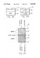
- the present inventionprovides for the fabrication of a micromechanical device (reference numeral 110; FIG. 8, 10I) for providing efficient steerable optical coupling with integrated circuitry.
- the micromechanical devicecomprises a movable platform supported by legs on a substrate.
- the substratehas one or more substrate electrodes and the platform has a bottom electrode.
- the platformis moved by applying a first electrical source between the first and bottom electrodes.
- a photonic deviceresides on the platform and is movable with the platform.
- the photonic devicehas a top electrode thereon. Further, the photonic device serves as a light interface, by emitting, receiving, or modulating light, when a second electrical source is applied between the top and the bottom electrodes.
- the present inventionovercomes the deficiencies of the prior art, as noted above, and further provides for the following features and advantages.
- An advantage of the novel processes of the present inventionis that they provide for the lift-off of any thin film material or device from a growth substrate, alignment of the same, and then selective bonding of the same to a host substrate.
- the thin film material and the host substratecan comprise any materials, including amorphous, polycrystalline, crystalline materials, or combinations thereof.
- Another advantage of the novel processes of the present inventionis that they provide a means for handling and bonding discrete devices which are too thin and delicate for manipulation by conventional means.
- Another advantage of the novel processes of the present inventionis that they provide for the lift-off and bonding of In x Ga 1-x As y P 1-y materials and devices (n-type or p-type), where 0 ⁇ x ⁇ 1 and 0 ⁇ y ⁇ 1, which are ideal for communications and optical applications.
- Another advantage of the novel processes of the present inventionis that they provide for selective alignment and selective bonding of particular devices from arrays of devices to existing circuitry. Moreover, contacts may be provided on both sides of the device.
- Another advantage of the novel processes of the present inventionis that material layers, such as metals, semiconductors, or dielectrics, can be easily applied to both sides of a thin film material or device, thereby potentially decreasing cost and improving performance.
- material layerssuch as metals, semiconductors, or dielectrics
- An exampleis a low cost, high performance, resonant cavity emitter, detector, or modulator.
- Another advantage of the novel processes of the present inventionis that they can be used to easily, inexpensively, and efficiently fabricate three dimensional communication networks within integrated circuits. As a result, massively parallel processing is possible, thereby enhancing processing speed.
- Optical detectors fabricated from semiconductor materialssuch as GaAs, InP, or InGaAsP based materials, can be integrated directly on top of an existing Si, GaAs, or Si substrate. Further, the Si substrate could have processing circuitry for processing signals received by individual optical detectors or aggregates thereof.
- Another advantage of the processes of the present inventionis that they can be utilized to fabricate micromechanical devices. Thin film materials or devices can be bonded to a very small movable element of the micromechanical device.
- Another advantage of the three dimensional integrated circuit cube of the present inventionis that it provides for massively parallel input/output (I/O) ports. Specifically, the number of I/O lines which can interface to an integrated circuit is substantially enhanced, because I/O contacts can be placed not only around the sides of the integrated circuit cube, but also on the top and bottom. These I/0 can be very fast, and optical I/0 as well. In essence, integrated circuit "cubes " are constructed.
- Another advantage of the three dimensional integrated circuit cube of the present inventionis that electronic circuits can be produced to occupy less space due to an enhanced three dimensional interconnection network.
- Another advantage of the three dimensional integrated circuit cube of the present inventionis that they can be fabricated from inexpensive Si and/or GaAs wafers.
- integrated circuitscan be first fabricated in an inexpensive manner using conventional Si or GaAs foundries. Then, optical emitters and/or detectors can be attached to the foundry Si or GaAs circuits in post-processing steps.
- Another advantage of the three dimensional integrated circuit cube of the present inventionis that the Si or GaAs circuitry and the emitters/detectors can be independently optimized and/or tested before integration for high yield and high performance.
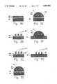
- FIG. 1shows a three dimensional integrated circuit cube having three dimensional electromagnetic communication capabilities throughout
- FIGS. 2A-2Cshow examples of various electromagnetic communication devices which are usable as emitters, detectors, or modulators within the three dimensional integrated circuit cube of FIG. 1 or in other various applications;
- FIG. 3A-3Gshow a first lift-off and bonding process for thin film materials or devices, such as the devices of FIGS. 2A-2C, wherein a carrier layer is utilized to lift-off and protect the thin film materials or devices;
- FIGS. 4A-4Hshow a second lift-off and bonding process for thin film materials or devices, such as the devices of FIGS. 2A-2C, wherein a transfer medium is utilized to transfer and invert the thin film materials or devices;
- FIG. 5shows an array of optical detectors
- FIG. 6shows a partial cross section of the array of optical detectors of FIG. 5 taken along line 6'--6';
- FIGS. 7A-7GShow a third lift-off and bonding process for producing the optical detectors of FIGS. 5 and 6;
- FIG. 8shows a micromechanical device
- FIG. 9shows a photonic device used in the micromechanical device of FIG. 8.
- FIGS. 10A-10IShow a fabrication process for producing the micromechanical device of FIG. 8, and specifically, FIG. 10I shows a cross section of the micromechanical device of FIG. 8 taken along line 10I'--10I'.
- FIG. 1illustrates a multilayered integrated circuit cube (IC), 10 wherein electromagnetic communication can occur in all directions throughout the three dimensional structure. Significantly, in addition to planar communication, vertical communication can occur directly through one or more integrated circuit layers 12, 14, thereby resulting in a truly three dimensional communication network. Although not shown for simplicity, the integrated circuit cube 10 can have numerous layers, and the principles described herein are equally applicable.
- ICintegrated circuit cube
- integrated circuit layerscommunicate via electromagnetic signals which can pass unhindered through the layers due to the wavelength associated with the electromagnetic signals.
- layers 12, 14are fabricated from Si, then the electromagnetic signals must have a wavelength ⁇ greater than 1.12 micrometers ( ⁇ m) in order for the Si to be transparent to the electromagnetic signals.
- the layers 12, 14are GaAs, then the wavelength ⁇ must be greater than 0.85 ⁇ m to establish transparency of the electromagnetic signals.
- many communications wavelengthsare possible depending upon the chemical composition of the layers 12, 14.
- the number of potential communication channelsis virtually infinite.
- electromagnetic communication devices 16-22are positioned throughout the integrated circuit cube 10 to permit communication throughout the cube 10, and importantly, to permit vertical communication through IC layers 12, 14.
- Each of the communication devices 16-22can be operated as an emitter, detector, or modulator, and these devices 16-22 communicate signals amongst each other as indicated by propagation arrows in FIG. 1.
- the electromagnetic communication devices 16-22can also be switched so as to operate as more than one of the foregoing communication elements. In other words, for example, any of the electromagnetic communication devices 16-22 could be switched to operate as both an emitter and a detector, or as a transceiver.
- FIGS. 2A through 2Cshow various specific examples of electromagnetic communication devices which can be used to implement the electromagnetic communication channels of FIG. 1.
- FIGS. 2A through 2Cillustrate devices having diode configurations. Each diode configuration can act as an emitter, detector, and/or modulator, which concept is well known in the art. Essentially, electromagnetic signals (including optical signals) are created, detected, or modulated by the diode configurations based upon the electrical biasing applied to the junction formed by the two materials adjoined in each of the diode configurations.
- diode configurations used for electromagnetic communications purposessee S. M. Sze, Physics of Semiconductor Devices(1981). It should be noted that the devices of FIGS. 2A-2C must be of very high quality in order to communicate at the wavelengths mentioned previously relative to Si ( ⁇ >l.12 ⁇ m) and GaAs ( ⁇ >0.85).
- FIG. 2Ashows a metal-semiconductor-metal (MSM) diode 33.
- MSMmetal-semiconductor-metal
- In x Ga 1-x As y P 1-y materials 28(n-type or p-type), where 0 ⁇ x ⁇ 1 and 0 ⁇ y ⁇ 1, are coupled to a metal 32, such as gold, silver, copper, aluminum, or the like.
- FIGS. 2Bshows another semiconductor diode 33.
- An n-type In x Ga 1-x As y P 1-y material 36where 0 ⁇ x ⁇ 1 and 0 ⁇ y ⁇ 1, is coupled to a p-type In x Ga 1-x As y P 1-y , material 38, where 0 ⁇ x' ⁇ 1 and 0 ⁇ y' ⁇ 1.
- FIG. 2Cshows a resonant cavity device 50 having an active region 56, mirrors 54 adjacent to the active region 56, and optional contact layers 58 adjacent to the mirrors 54.
- the active region 56can be a diode configuration, for example, one of those diode configurations shown in FIGS. 2A or 2B, or some other suitable element which emits, detects, or modulates electromagnetic energy.
- Mirrors 54may comprise any metal, semiconductor, or dielectric layer, or combinations thereof, but preferably is a plurality of In x Ga 1-x As y P 1-y semiconductor layers where 0 ⁇ x ⁇ 1 and 0 ⁇ y ⁇ 1for providing essentially signal frequency filtering, which concept and implementation is well known in the art.
- the vertical span of the mirrors 54, or the distance between each metal layer 58 and the active region 56determines the wavelength of signal which is received with the highest signal intensity.
- the contact layers 58may comprise a metal, semiconductor, or dielectric layer, or combinations thereof, but preferably is a metal layer, for biasing the device 50 so that it responds as an emitter, detector, or modulator.
- the device 50may be biased by some other means, such as with an optic beam, in which case, the contacts 58 are not required for operation of the device 50.
- the diode configurationis first biased with a voltage. Propagation or reception depends, in large part, upon the device design and direction of voltage biasing.
- the diode configurations of FIG. 2A through 2Cwill send and receive electromagnetic signals having wavelengths ⁇ between 1.3 and 1.55 microns, which is well above the Si and GaAs transparency wavelength thresholds of 1.12 and 0.85 microns, respectively. Note that communication is possible using different emitter and detector types, depending upon the materials utilized in the configuration.
- modulatorsfor instance, multiple quantum well (MQW) reflective electroabsorption light modulators, that emitters, for instance, surface emitting lasers (SELs) and vertical cavity surface emitting lasers (VCSELs), and that detectors, for instance, resonant cavity detectors which are developed from In x Ga 1-x As y P 1-y compounds, where 0 ⁇ x ⁇ 1 and 0 ⁇ y ⁇ 1, can be employed to more efficiently communicate the signals in the three dimensional integrated circuit cube 10 of FIG. 1. These devices cause less heating problems and can switch much faster than diode configurations.
- SELs and VCSELscan be found in IEEE Journ. Quant. Elect., Vol. 64, No. 6, Special Issue on Semiconductor Lasers, 1991, and J. Jewell, J. Harbison, A. Scherer, Y. Lee and L. Florez, IEEE Journal Quant. Elect., Volume 7, No. 6, pp. 1332-1346.
- the bonding of high quality In x Ga 1-x As y P 1-y based materials and devices to host substratesis a key element to the realization of the diode configurations of FIGS. 2A-2C and the envisioned laser configurations, and more generally, to the realization of three dimensional IC cubes and other applications in accordance with the present invention.
- the inventorshave developed several advanced lift-off and bonding processes 60, 80, 100 discussed in detail hereafter. These processes 60, 80, 100 generally provide for lifting-off and subsequent bonding of thin film materials or devices, such as compound semiconductors, having a thickness of typically less than 20 micrometers.
- FIGS. 3A through 3Gillustrate a first lift-off and bonding process 60 wherein a carrier layer 74 is utilized to lift off, protect, transport, align, and ultimately bond thin film materials 66 or devices 68, including compound semiconductors.
- a growth substrate 62is provided with a sacrificial layer 64 and a thin film material 66.
- the sacrificial layer 64 and material 66are deposited on the growth substrate 62 using any conventional technique.
- the material 66can be any material, including amorphous material, polycrystalline material, crystalline material (for example, an epitaxial material), or combinations of the foregoing materials.
- depositingin the context of this document refers to any process for growing or forming one material on another as in the case of an epitaxial material.
- the growth substrate 62is GaAs.
- the sacrificial layer 64is a thin layer of aluminum gallium arsenide Al x GA 1-x As, where 0.6 ⁇ x ⁇ 1.0.
- the material 66comprises In x Ga 1-x As y P 1-y (n-type or p-type), where 0 ⁇ x ⁇ 1 and 0 ⁇ y ⁇ 1.
- mesa etch processingmay be employed to pattern the material 66 in order to form one or more devices 68.
- the discussion hereafterrefers only to the devices 68 and not to the material 66, but it should be understood that the discussion is equally applicable to the material 66 in an unpatterned state.
- FIG. 3Bshows several devices 68 to emphasize that, in general, the process 60 is performed on a mass scale to produce large pluralities of the devices 68 at a time.
- the devices 68can be, for example, a transistor, diode configuration, communication device, compound semiconductor device, or any other desired device.
- the mesa etchuses, for example, a photoresist mask and is performed using, for instance, H 2 SO 4 :H 2 O 2 :H 2 O(l:8:160) as a fast gross etch with a final selective etch of NH 4 OH:H 2 O 2 (1:200) which stops at the AlAs sacrificial layer 64.
- one or more material layers 72can be deposited on the devices 68.
- the material layers 72may comprise metals (for contacts, as an example), semiconductors, or dielectrics. Deposition of the material layers 72 can occur using any of numerous conventional techniques. In the preferred embodiment, material layers 72 are deposited on the devices 68 via vacuum deposition.
- the devices 68, with or without material layers 72,are completely coated with a carrier layer 74.
- the carrier layer 74is either a transparent polyimide or other organic material which itself can be made to act as a release layer.
- Apiezon Wwhich is essentially a black, opaque wax, can also be utilized as described in U.S. Pat. No. 4,846,931 to Gmitter et al. of Bellcore.
- the carrier layer 74could be a metal, which has been evaporated, sputtered, and/or plated over the devices 68.
- use of a transparent polyimideis preferred for several reasons.
- polyimidesexhibit the desirable mechanical property of being under residual tensile stress at room temperature. See Allen, M. G., Mehregany, M., Howe, R. T., and Senturia, S. D., "Microfabricated Structures for the In-Situ Measurement of Residual Stress, Young's Modulus, and Ultimate Strain of Thin Films, " Applied Physics Letters, Volume 51, No. 4, pp. 241-244, 1987. Finally, the thermal properties of polyimides are excellent. Temperatures in excess of 400° C. can be maintained without damage to the polyimide or devices 68 protected thereby.
- the sacrificial layer 64is etched away using a standard HF:H 2 O (1:10) etch solution to separate the devices 68 and surrounding carrier layer 74 from the growth substrate 62, as shown in FIG. 1E.
- metal layerse.g., Al
- Al x Ga 1-x As layers where x>0.4can be included in the devices 68, because the devices 68 are protected on their sides from the etch solution HF:H 2 O (1:10) by the carrier layer 74.
- the combination of the devices 68 and the carrier layer 74After the combination of the devices 68 and the carrier layer 74 has been etched away from the substrate 62, the combination can easily be handled and transported.
- the devices 68are next placed in contact with a host substrate 84, as shown in FIG. 3F. If the carrier layer 74 is a transparent polymer, alignment of the devices 68 with particular circuitry on the host substrate 84 is easily accomplished.
- the devices 68are bonded to the host substrate 84 by a variety of forces, including vander Waals bonding and metal-metal annealing. "Bonding " means affixing, adhering, or otherwise attaching one existing material or device to another.
- the carrier layer 74is dissociated from the devices 68.
- the dissociationcan be effectuated using many techniques.
- the procedure in FIG. 3Gis performed within a clean room.
- the host substrate 84can comprise a Si or GaAs circuit which has been developed and optimized, in perhaps a foundry, independent of the devices 68.
- An oven-annealing stepmay be desirable at this point to further consolidate and strengthen the bonds between the devices 68 and the host substrate 84. Furthermore, a whole-wafer cleaning might also be carried out to remove any residual material from the carrier layer 74.
- a peripheral frame(not shown) can be bonded to the carrier layer 74 before the growth substrate 62 is freed.
- the peripheral framecan help in handling and aligning the devices 68.
- the assemblywould resemble a mounted pellicle after release from the growth substrate 62.
- FIGS. 4A through 4Hillustrate a second lift-off and bonding process 80 utilizing a transfer medium for transporting and inverting the devices 68.
- the second lift-off and bonding process 80may be used to fabricate the electromagnetic communication devices 27, 33, 50 of FIGS. 2A-2C.
- the second lift-off and bonding process 80calls for placing the freely maneuverable combination of the devices 68 and the carrier layer 74 onto a transfer medium 76, which in the preferred embodiment, is a diaphragm assembly comprising a diaphragm 78 and support ring 82.
- the diaphragm assembly 76is a drum-like structure fabricated using any standard micromachining techniques.
- the diaphragm assembly 76is formed by first coating a Si wafer with approximately 4 microns of a transparent polyimide.
- the transparent polyimideis spin cast from a commercially available polymeric acid solution (DuPont PI 2611) which is baked at 150° C. in air for 30 minutes and cured at 400° C. in nitrogen for 1 hour.
- the central portion of the Si waferis etched from the backside using a HF:HNO 3 :H 2 O etchant using a single-sided etching technique.
- a single-sided etching technique for this purposeis disclosed in J. Y. Pan and S. D.
- the etching processresults in the diaphragm assembly 76 having a polymeric diaphragm 78, which measures approximately 4 ⁇ m thick and 3-25 millimeters (mm) in diameter, and which is supported by a Si ring 82.
- the polymeric diaphragm 78is transparent, taut, and mechanically tough.
- the polymeric diaphragm 78is ideal as a carrier for the devices 68.
- a low power oxygen plasma etchis performed on the diaphragm 78 prior to bonding of the devices 68.
- the oxygen plasma etchenhances the adhesion of the devices 68 to the diaphragm 78.
- the carrier layer 74is dissolved while affixed to the diaphragm assembly 76.
- trichloroethyleneis used to dissolve the Apiezon W.
- the devices 68are left alone bonded to the top of the polymeric diaphragm 78.
- the prelift-off processing materialsfor example, the material layers 72, now reside on the top of the devices 68 supported by the polymeric diaphragm 78.
- the devices 68can now be selectively aligned through the transparent polymeric diaphragm 78 and bonded to a host substrate 84.
- one or more devices 68', 68"can be selectively bonded from an array of devices 68 as illustrated in FIG. 4G, or alternatively, the entire array of devices 68 can be bonded concurrently to the host substrate 84.
- the process shown in FIG. 4Gis performed within a clean room.
- the host substrate 84can comprise a circuit containing a Si or a GaAs substrate which has been developed, perhaps in a foundry, independent of the devices 68.
- the bonding of the devices 68 to the host substrate 84can be effectuated via many techniques. All techniques for causing release of the devices 68, which were described above in regard to the first lift-off and bonding process 60 of FIGS. 3A-3G, can be utilized in the second lift-off and bonding process 80 of FIGS. 4A-4H.
- the polymeric diaphragm 78can be etched away around the devices 68 so as to release the devices 68 onto the host substrate 84.
- the polymeric diaphragm 78could be fabricated in a web-like manner so as to facilitate tearing and release of the devices 68.
- the diaphragm assembly 76may be placed in a mask aligner. With the diaphragm assembly 76 in a mask aligner, the devices 68 can be positioned on the host substrate 84 with a high precision (at least to within 1 ⁇ m).
- Another feature of the second lift-off and bonding process 80is that the devices 68 with material layers 72 can be bonded directly to metal contact layers 86 situated at the top surface of the host substrate 84, as illustrated by device 68" in FIG. 4G. If the material layer 72 of device 68" is metal, then the coupling of the material layers 72 and the metal contact layer 86 associated with the device 68" forms a much better electrical bond therebetween, than merely a vander Waals bond, generally because of the surface characteristics of metals. Additionally, if the material layer 72 is metal, it can be fused with the metal contact layer 86 via a heating process so as to further enhance the electrical characteristics of the connection.
- one or more other material layers 88such as a metal, semiconductor, or dielectric layer, or combinations thereof, may be deposited upon the devices 68 after the devices 68 are bonded to the host substrate 84 or to the layer 86 on the host substrate 84.
- the foregoing second lift-off and bonding process 80allows material layers, such as metal, semiconductor, or dielectric layers, to be deposited on both sides of each of the devices 68, as illustrated by the device 68' in FIG. 4H.
- the resonant cavity device 50 of FIG. 2Cwhich has mirror layers 54 on both planar sides of a thin film active region 56, may be constructed using the foregoing methodology.
- the devices 68are supported by a substrate (either the growth substrate 62 or host substrate 84) during the deposition process on each side, thereby providing mechanical support to the devices 68 while the potentially stress and/or strain producing layers 88, 72 are deposited onto the devices 68.
- a substrateeither the growth substrate 62 or host substrate 84
- an array 90 of optical detectors 98can be bonded to any suitable substrate in accordance with the novel processes 60, 80, 100 of the present invention.
- Such an array 90would have many advantages.
- the optical detectors 98can be configured to simultaneously receive optical signals 91 from an image.
- the optical signals 91are then processed massively in parallel so as to gain a substantial speed advantage in processing, and consequently, real time evaluation of the image.
- FIG. 6shows a partial cross-section of the array 90 taken along line 6'--6'.
- the array 90is fabricated by first applying an insulating layer 92, such as a polyimide layer, on the host substrate 84, which has optical signal processing circuitry 84'.
- the host substrate 84can be Si, GaAs, or any other suitable substrate material.
- the polyimide layer 92can be about 1-4 microns in thickness.
- holes 94are cut into the polyimide layer 92.
- the holes 94are filled or partially filled with metal or metal alloy, preferably gold (Au) to form interconnects 96.
- the thin film optical detectors 98comprising, for instance, In x Ga 1-x As y P 1-y (n-type or p-type) where 0 ⁇ x ⁇ 1 and 0 ⁇ y ⁇ 1, a diode configuration, or some other suitable semiconductor, are bonded to the metal interconnects 96 using one of the lift-off and bonding processes 60, 80 disclosed herein.
- the metal interconnects 96serve the purpose of creating a MSM diode junction, as shown and described relative to FIG. 2A, and serve the purpose of communicating signals to the underlying processing circuitry 84' within the host substrate 84. If the optical detectors 98 are junction or diode devices, as shown and described relative to FIG. 2B, then the metal interconnects 96 serve to connect the detectors 98 to the underlying processing circuitry 84'. Because the metal interconnects 96 are extremely short, for example, about 1-2 microns, virtually no parasitic capacitance will hinder the speed of the optical detectors 98.
- Each of the optical detectors 98can be allocated its own processing circuitry 84', as further shown in FIG. 6. Essentially, the processing circuitry 84' can directly and immediately process the optical signals 91.
- a neural networkcan be situated in the host substrate 84.
- the datacould be partially processed by the host substrate 84, and then the optical signal data could be sent to a remote neural network or another substrate.
- the processing circuitrycould also be configured in hierarchical layers. In other words, another layer of processing circuitry (not shown) could integrate the results of the various elements of processing circuitry 84'.
- the array 90 of optical detectors 98 described in relation to FIGS. 5 and 6can be produced by using the novel processes 60, 80 of respective FIGS. 3 and 4. However, in addition, the inventors have developed a third lift-off and bonding process 100 directed to producing an array 90 of detectors 98 having In x Ga 1-x As y P 1-y .
- FIGS. 7A, 7B, 7CThe steps of the process which are shown in FIGS. 7A, 7B, 7C are substantially similar to the steps shown and described relative to, respectively, FIGS. 3A, 3B, 3D and 4A, 4B, 4D. Therefore, the discussion in regard to the latter figures is incorporated herein and applies to the third lift-off and bonding process 100 of FIG. 7. Briefly described, referring to FIG. 7A, a growth substrate 62 is provided with a sacrificial layer 64 and a thin film material 66. In the process of FIG.
- the growth substrate 62is InP
- the sacrificial layer 64is In x Ga 1-x As y P 1-y material, where 0 ⁇ x ⁇ 1 and 0 ⁇ y ⁇ 1, which is grown on the growth substrate 62
- the material 66is a In x Ga 1-x As y P 1-y material, where 0 ⁇ x ⁇ 1 and 0 ⁇ y ⁇ 1which is grown on the sacrificial layer 64.
- Mesa etch processingis then used to define, or pattern, the detectors 98 from the material 66, as illustrated in FIG. 7B.
- the detectors 98are then completely coated with the carrier layer 74 in order to encapsulate the devices 98 on the growth substrate 62, as shown in FIG. 7C.
- the InP growth substrate 62is etched away with a first etch solution.
- the first etch solutioncan be, for example, HCl:H 3 PO 4 (3:1).
- the first etch solutiondoes not affect the InGaAsP sacrificial layer 64, as shown in FIG. 7D.
- the InGaAsP sacrificial layer 64can be left with and used as part of the detectors 98 for the purpose of aiding emission, detection, or modulation.
- a second etch solutionwhich can be, for example, HF:H 2 O 2 :H 2 O (1:1:10) or H 2 SO 4 :H 2 O 2 :H 2 O (1:1:1) in the preferred embodiment, can be applied to remove the InGaAsP sacrificial layer 64, as illustrated in FIG. 7E.
- Metals, semiconductors, and/or dielectric layerscan be deposited onto both sides of the detectors 98 as outlined above in the discussion of the second lift-off and bonding process 80.
- the detectors 98can be selectively aligned and selectively bonded to any location on the host substrate 84.
- the transfer medium 76can be used to invert the detectors 98 before bonding them to the host substrate 84.
- micromechanical deviceis a device which is fabricated using integrated circuit technology or related arts and which performs transduction of electrical energy to mechanical energy, or vice versa.
- micromechanical devicesmust comprise a movable element(s).
- thin film materials or devicesare formed and optimized on a growth substrate and are then bonded to the movable element(s) of a micromechanical device.
- a micromechanical device 110 of the preferred embodimenthas a thin film photonic device 112 on a generally square movable platform 114, which is supported by elongated legs 144a-144d above a substrate 134.
- a movable micromechanical platform with support legssimilar to the platform 114 of the present invention, has been produced previously in the art. See Y. W. Kim and M. G. Allen (a co-inventor herein), "Single and Multilayer Surface Micromechanical Platforms Using Sacrificial Layers," Sensors and Actuators, Vol. 35, No. 1, October 1992, pp. 61-68. Through the appropriate application of external voltages of typically around 35 V, the prior art platform can be actuated in both the vertical and lateral directions by as much as approximately 5 ⁇ m and 15 ⁇ m, respectively.
- the micromechanical device 110 of the present inventionis fabricated by producing the photonic device 112 independently of the platform 114 and associated structure.
- the photonic device 112is fabricated and then bonded to the platform 114 in accordance with the methodology of the second lift-off and bonding process 80 of FIGS. 4A-4H, which process utilizes the novel transfer medium 76. Accordingly, the discussion details relative to the second lift-off and bonding process 80 of FIGS. 4A-4H is incorporated herein by reference, and therefore only a brief overview of the procedure for fabricating and bonding the photonic device 112 is set forth hereafter for simplicity.
- the photonic device 112comprises a AlGaAs/GaAs/AlGaAs double heterostructure, which can be employed as 1.3 ⁇ emitter, detector, or modulator by applying certain voltage biases.
- the as-grown layer structure 113 of the photonic device 112is illustrated in FIG. 9. As shown in FIG. 9, an undoped AlAs sacrificial layer 118 with 0.2 ⁇ m thickness is grown lattice matched to a GaAs growth substrate 116. The photonic device 112 is then grown lattice matched on top of the AlAs sacrificial layer 118.
- the successive device layers 124, 126, 128are mesa etched with a combination of nonselective and selective GaAs/AlGaAs etchants.
- a AuZn/Au metallic electrode 128is bonded and patterned on the device layer 126 using standard photolithographic techniques and metal etches. Although the metallic electrode 128 is initially on top of the as-grown structure 113, the device 112 with metallic electrode 128 is inverted when bonded by the transfer medium 76 (FIG. 4F and 4G) so that the metallic electrode 126 eventually resides on the bottom of the device 112 in the final integration. Therefore, the metallic electrode 128 is referred to as the bottom electrode of the photonic device 112.
- the photonic device 112is coated with a carrier layer of Apiezon W black wax, and the entire as-grown structure 113 is immersed in 10% HF to selectively etch away the AlAs sacrificial layer 118. After separation from the growth substrate 116, the photonic device 112 is bonded to the transfer medium 76.
- the transfer medium 76preferably comprises the transparent polyimide diaphragm 78 so that the device 112 can be accurately and selectively aligned during bonding of the device 112 on the host substrate. After positioning and aligning the device 112, the photonic device 112 is bonded to the moveable platform 114 of the photonic device 112.
- the platform 114is fabricated using standard micromachining techniques, as will be described relative to FIGS. 10A-10I.
- a plurality or array of Au strip-like substrate electrodes 132are defined on an electrically isolated Si wafer 134. These substrate electrodes 132 are insulated with a polyimide layer 136 which is bonded over the substrate electrodes 132, as shown in FIG. 10B.
- a copper (Cu) release layer 138is bonded on top of the polyimide layer 136.
- at least one and preferably three layers 142 of polyimideare spun onto the Cu release layer 38.
- the polyimide layer(s) 142essentially produces the supporting infrastructure of the top platform 114 and the support legs 144a-144d.
- the platform sizeis 360 ⁇ m ⁇ 360 ⁇ m or 200 ⁇ m ⁇ 200 ⁇ m having respective leg widths of 20 ⁇ m and 40 ⁇ m for receiving a photonic device 112 having a respective size of 250 ⁇ m ⁇ 250 ⁇ m or 100 ⁇ m ⁇ 100 ⁇ m.
- the polyimide layer(s) 142is coated with a gold (Au) layer 146.
- the Au layer 146is bonded across the entire top surface of the layer(s) 142 and on the top surfaces of the opposing legs 144a, 144c, as shown in FIG. 8.
- the Au layer 146facilitates bonding of the photonic device 112 to the platform 114 by easily bonding or fusing with the AuZn/Au metallic bottom electrode 128 of the photonic device 112.
- the Au layer 146 in combination with the AuZn/Au layer 128form the ultimate bottom electrode of the micromechanical device 110.
- the bottom electrodeis electrically accessible at the surface of the substrate 134 as a result of the interconnecting paths running along legs 144a, 144c.
- the photonic device 112is bonded to the platform 142 using the transfer medium 76, as illustrated in FIG. 10F.
- the procedureis described in detail relative to FIGS. 4F and 4G.
- a polyimide insulating layer 148is spun over the exposed regions of the platform 114 and the photonic device 112, and a top access window 152 to the photonic device 112 is opened using any suitable technique, for instance, a reactive ion etching (RIE) technique.
- RIEreactive ion etching
- a top electrode 154 of the micromechanical device 110is now defined in the step shown in FIG. 10H.
- the top electrode 154is defined so that the electrode 154 covers the top surface perimeter around the photonic device 112 and runs along the top surfaces of the two opposing legs 144b, 144d of the platform 114, as illustrated in the top view of FIG. 8.
- the copper release layer 138is removed from the substrate 134 by etching away the copper release layer 138 with a FeCl 3 solution, resulting in the micromechanical device 110 having a platform 114 with an integrated thin film photonic device 112.
- the photonic device 112may be electrically operated by applying voltages to the three available electrical electrode sources: the substrate electrodes 132, the bottom electrode 128, and the top electrode 154.
- the bottom and top electrodes 128, 154can be probed via respective pads 156a, 156c and 156b, 156d at the ends of the respective platform legs 144a, 144c and 144b, 144d.
- an electrical sourcesuch as a voltage or current source
- the platform 114is moved vertically and/or laterally.
- the platform 114can be moved in a plurality of vertical and/or lateral directions as a result of the spaced array of substrate electrodes 132, which may be selectively energized.
- the micromechanical device 110 of the present inventionhas many advantages over the prior art.
- Previous work aimed at producing micromechanical devices with photonic elementshas been focused almost exclusively on the micromachining of gallium arsenide or other compound semiconductor materials which can emit light.
- these prior art embodimentslack the excellent mechanical properties of silicon and do not have established micromachining or circuit fabrication facilities as compared with silicon.
- a micro-opto-mechanical systemis formed which combines the ability to conduct and steer light with all of the advantages of silicon.
- the micromechanical device 110in accordance with the present invention provides a much more economical and efficient coupling solution.
- the micromechanical device 110can be used to automatically align an emitter/detector with an optical fiber by holding the optical fiber stationary while moving the photonic device 112 via electrical control signals applied to the substrate electrodes 132 and the bottom electrode 146.
- micromechanical device 110Other applications for the micromechanical device 110 include interferometric devices, such as accelerometers, and communications applications where receiver selective reception of light signals of various wavelengths is required.
- interferometric devicessuch as accelerometers, and communications applications where receiver selective reception of light signals of various wavelengths is required.
- the micromechanical device 110is moved, and during movement, inertia causes the platform 114 and the photonic device 112 to move, thereby changing the shape of the cavity 138' beneath the platform 114.
- This change in cavity shapecan be used to either control the wavelength of light to which a detector is sensitive or to control the frequency of operation of an emitter.
- the transmissive characteristics of the optical system made of device 112, cavity 138', and substrate 134are altered due to the change in size of cavity 138'.
- the micromechanical device 110can be operated like a filter.
- the photonic device 112is positioned a particular distance above the substrate 134 so that only a certain wavelength or bandwidth of light is received for processing.
Landscapes
- Engineering & Computer Science (AREA)
- Physics & Mathematics (AREA)
- Manufacturing & Machinery (AREA)
- Condensed Matter Physics & Semiconductors (AREA)
- General Physics & Mathematics (AREA)
- Microelectronics & Electronic Packaging (AREA)
- Power Engineering (AREA)
- Computer Hardware Design (AREA)
- Optics & Photonics (AREA)
- Electromagnetism (AREA)
- Semiconductor Lasers (AREA)
- Solid State Image Pick-Up Elements (AREA)
- Optical Integrated Circuits (AREA)
- Photo Coupler, Interrupter, Optical-To-Optical Conversion Devices (AREA)
Abstract
Description
The U.S. Government has a paid-up license in this invention and the right in limited circumstances to require the patent owner to license others on reasonable terms as provided by the terms of Contract Number ECS90-58-144 awarded by the National Science Foundation.
This document is a continuation-in-part of U.S. application Ser. No. 07/865,379 filed Apr. 8, 1992, by the same inventors herein for THREE DIMENSIONAL INTEGRATED CIRCUITS, now U.S. Pat. No. 5,280,184, and of U.S. application Ser. No. 07/865,126 filed Apr. 8, 1992, by the same inventors herein for PROCESSES FOR LIFT-OFF 0F THIN FILM MATERIALS AND FOR THE FABRICATION OF THREE DIMENSIONAL INTEGRATED CIRCUITS, now U.S. Pat. No. 5,244,818.
The present invention generally relates to integrated circuit technology, and more particularly, to novel processes for the lift-off of any thin film material or device from a growth substrate and alignable bonding of the same to a host substrate as well as to the implementation of three dimensional integrated circuit cubes, resonant cavity devices, optical detectors, and micromechanical devices using the foregoing novel processes.
The monolithic integration of gallium arsenide (GaAs) materials and devices with host substrates, such as silicon (Si), glass (SiO2), and polymers, will enable the fabrication of the next generation of integrated circuits, optical devices, and micromechanical devices, because it is known that Inx Ga1-x Asy P1-y materials, where 0<x<1 and 0<y<1, and devices comprising the foregoing materials are ideal for electromagnetic communications applications.
A standard technique for GaAs on Si integration is heteroepitaxial growth, which is described in H. Choi J. Mattia, G. Turner, and B. Y. Tsauer, "Monolithic Integration of GaAs/AlGaAs LED and Si Driver Circuit", IEEE Electron Dev. Lett., vol.9, pp. 512-514, 1988. However, the crystal quality of this heteroepitaxial material is often inadequate for many optical applications.
An integration method which seeks to preserve the high material quality of lattice-matched growth is the epitaxial lift-off process developed by Bell Communications Research, Inc., (Bellcore), as described in E. Yablonovitch, T. J. Gmitter, J. P. Harbison, and R. Bhat, "Double Heterostructure GaAs/AlGaAs Thin Film Diode Lasers on Glass Substrates", IEEE Phot. Tech. Lett., 1, pp. 41-42, 1989. Essentially, a thin aluminum arsenide (AlAs) sacrificial layer is deposited, or grown, on a GaAs substrate, and then GaAs/AlGaAs device epitaxial layers are grown on top of the AlAs layer. The GaAs/AlGaAs lattice-matched epitaxial layers are separated from the growth substrate by selectively etching the AlAs sacrificial layer. These device layers are then mounted in a hybrid fashion onto a variety of host substrates. The device layers are of high quality and are currently being used for the integration of GaAs/AlGaAs materials with host substrates, such as Si, glass, lithium niobate, and polymers.
However, although the Bellcore technique yields high quality material, it has several problems, including the inability to align and selectively bond the devices. Moreover, there are difficulties in contacting and depositing material layers on both sides of the devices. Hence, at present, the Bellcore technique is inadequate for producing emitters, detectors, and modulators for three dimensional integrated circuits.
The present invention provides various novel processes for monolithically integrating any thin film material or any device, including semiconductors and compound semiconductors. The processes involve separation, or "lift-off, " of the thin film material or device from a growth substrate, selective alignment of the same, and then selective bonding of the same to a host substrate. Significantly, the novel processes may be utilized to produce and bond high quality emitters, detectors, or modulators for implementing three dimensional communication, and consequently, the fabrication of three dimensional integrated circuit cubes is realized. Other various optical applications are also contemplated as described herein. Moreover, the processes may be utilized in the fabrication of micromechanical devices.
In accordance with the present invention, a first lift-off and bonding process (reference numeral 60; FIGS. 3A-3G) comprises the following steps. A thin film material is deposited on a sacrificial layer situated on a growth substrate. Optionally, a device may be defined or patterned in the thin film material. All exposed sides of the material or device, if applicable, are coated with a transparent carrier layer. The sacrificial layer is then etched away to release from the growth substrate the combination of the transparent carrier layer and either the material or the device. The material or device can then be selectively aligned and bonded to a host substrate. If the carrier layer comprises a plurality of devices, then they can be selectively bonded to the host substrate. Finally, the transparent carrier layer is removed, thereby leaving the material or device on the host substrate.
In accordance with the present invention, a second lift-off and bonding process (reference numeral 80; FIGS. 4A-4H) comprises the following steps. A thin film material is deposited on a sacrificial layer situated on a growth substrate. Optionally, a device may be defined, or patterned, in the thin film material. All exposed sides, or the exposed region, of the material or device, if applicable, are coated with a carrier layer. The sacrificial layer is etched away to release the combination of the material or device and the carrier layer from the growth substrate. The material or device is then bonded to a transfer medium. The carrier layer is removed. Finally, the material or device is aligned and selectively bonded to a host substrate from the transfer medium.
In accordance with the present invention, a third lift-off and bonding process (reference numeral 100; FIGS. 7A-7G) comprises the following steps. A thin film material is deposited on a sacrificial layer which is deposited on a growth substrate. Optionally, a device may be defined, or patterned, in the thin film material. All exposed sides, or the exposed region, of the material or device, if applicable, are coated with a carrier layer. The growth substrate is etched away. The sacrificial layer may be retained or is etched away. The device is bonded to a transfer medium. The carrier layer is removed. Finally, the material or device is aligned and bonded to the host substrate from the transfer medium.
The present invention provides for three dimensional integrated circuit cubes (reference numeral 10; FIG. 1) and other applications via the aforementioned novel lift-off and bonding processes. These processes are used for monolithically integrating thin film electromagnetic emitters, detectors, or modulators. In a monolithic three dimensional integrated circuit cube fabricated in accordance with the present invention, electromagnetic communication occurs vertically through any integrated circuit layer(s), which can have operational circuitry, and/or occurs laterally in the same integrated circuit layer. Electromagnetic signals are sent from an emitter and received by one or more detectors situated at some other location anywhere in the integrated circuit cube.
In basic concept, the three dimensional integrated circuit cube can be described as follows. A first integrated circuit layer in the three dimensional integrated circuit has a first and a second side. An emitter situated either on the first side or on a layer spaced from the first integrated circuit layer sends electromagnetic signals towards the direction of the first side. The emitter can have an emitting junction, for example, created by Inx Ga1-x Asy P1-y materials (n-type coupled to p-type), where 0<x<1 and 0<y<1. The signals sent from the emitter pass through one or more layers because the layers are transparent to the carrier frequency of the signals. A detector is situated to receive the electromagnetic signals from the direction of the second side. The detector can be situated on the second side of the integrated circuit layer or on a different layer in the integrated circuit. Moreover, the detector can have a detecting junction, for example, that may be created by the materials used in the emitter. Worth noting is that the emitter and detector may be identical except for electrical excitation, and may be freely interchanged by changing electrical excitation so as to further increase the flexibility of the proposed invention. Finally, the foregoing emitters and detectors can be situated anywhere throughout the integrated circuit so as to provide for a very complex and flexible three dimensional communication network.
The present invention provides for the fabrication of a high performance resonant cavity device (reference numeral 50; FIG. 2C), which can be operated as an emitter, detector, or modulator. The resonant cavity device comprises an active region having a first side and a second side. The active region may have a diode configuration or some other element which emits, detects, or modulates electromagnetic energy. A first mirror layer is situated adjacent to the first side of the device and is deposited after the active region is deposited on a first substrate. A second mirror layer is situated adjacent to the second side and is deposited after the active region with the first mirror layer are bonded to a second substrate.
The present invention provides for the fabrication of an array of optical detectors (reference numeral 90; FIGS. 5, 6) for an imaging or video system. The array of optical detectors is monolithically formed on an external surface of an integrated circuit. Each integrated layer has a polyimide or other electrically insulating layer with a top and a bottom and a hole therethrough leading to processing circuitry. The thin film detectors, placed on top of the polyimide or other electrically insulating layer, convert the optical signal to an electrical signal. The processing circuitry is configured to process the converted optical signals. The hole is filled with a conductor configured to transport the converted optical signals to the processing circuitry. The detectors can be made of an epitaxial layer, for example, comprised of either GaAs, InP or InGaAsP situated at the top of the polyimide layer in contact with the metal. The epitaxial layer alone can create a detecting junction, or the epitaxial layer in combination with the metal can create a detecting junction which receives optical signals from an exterior source and immediately transmits the signals to the processing circuitry.
The present invention provides for the fabrication of a micromechanical device (reference numeral 110; FIG. 8, 10I) for providing efficient steerable optical coupling with integrated circuitry. The micromechanical device comprises a movable platform supported by legs on a substrate. The substrate has one or more substrate electrodes and the platform has a bottom electrode. The platform is moved by applying a first electrical source between the first and bottom electrodes. Moreover, a photonic device resides on the platform and is movable with the platform. The photonic device has a top electrode thereon. Further, the photonic device serves as a light interface, by emitting, receiving, or modulating light, when a second electrical source is applied between the top and the bottom electrodes.
The present invention overcomes the deficiencies of the prior art, as noted above, and further provides for the following features and advantages.
An advantage of the novel processes of the present invention is that they provide for the lift-off of any thin film material or device from a growth substrate, alignment of the same, and then selective bonding of the same to a host substrate. The thin film material and the host substrate can comprise any materials, including amorphous, polycrystalline, crystalline materials, or combinations thereof.
Another advantage of the novel processes of the present invention is that they provide a means for handling and bonding discrete devices which are too thin and delicate for manipulation by conventional means.
Another advantage of the novel processes of the present invention is that they provide for the lift-off and bonding of Inx Ga1-x Asy P1-y materials and devices (n-type or p-type), where 0<x<1 and 0<y<1, which are ideal for communications and optical applications.
Another advantage of the novel processes of the present invention is that they provide for selective alignment and selective bonding of particular devices from arrays of devices to existing circuitry. Moreover, contacts may be provided on both sides of the device.
Another advantage of the novel processes of the present invention is that material layers, such as metals, semiconductors, or dielectrics, can be easily applied to both sides of a thin film material or device, thereby potentially decreasing cost and improving performance. An example is a low cost, high performance, resonant cavity emitter, detector, or modulator.
Another advantage of the novel processes of the present invention is that they can be used to easily, inexpensively, and efficiently fabricate three dimensional communication networks within integrated circuits. As a result, massively parallel processing is possible, thereby enhancing processing speed.
Another advantage of the processes of the present invention is that they provide for extensive image processing and video applications. Optical detectors fabricated from semiconductor materials, such as GaAs, InP, or InGaAsP based materials, can be integrated directly on top of an existing Si, GaAs, or Si substrate. Further, the Si substrate could have processing circuitry for processing signals received by individual optical detectors or aggregates thereof.
Another advantage of the processes of the present invention is that they can be utilized to fabricate micromechanical devices. Thin film materials or devices can be bonded to a very small movable element of the micromechanical device.
Another advantage of the three dimensional integrated circuit cube of the present invention is that it provides for massively parallel input/output (I/O) ports. Specifically, the number of I/O lines which can interface to an integrated circuit is substantially enhanced, because I/O contacts can be placed not only around the sides of the integrated circuit cube, but also on the top and bottom. These I/0 can be very fast, and optical I/0 as well. In essence, integrated circuit "cubes " are constructed.
Another advantage of the three dimensional integrated circuit cube of the present invention is that electronic circuits can be produced to occupy less space due to an enhanced three dimensional interconnection network.
Another advantage of the three dimensional integrated circuit cube of the present invention is that they can be fabricated from inexpensive Si and/or GaAs wafers. In other words, integrated circuits can be first fabricated in an inexpensive manner using conventional Si or GaAs foundries. Then, optical emitters and/or detectors can be attached to the foundry Si or GaAs circuits in post-processing steps.
Another advantage of the three dimensional integrated circuit cube of the present invention is that the Si or GaAs circuitry and the emitters/detectors can be independently optimized and/or tested before integration for high yield and high performance.
Further features and advantages of the present invention will become apparent to one skilled in the art upon examination of the following drawings and the detailed description. It is intended that any additional features and advantages be incorporated herein.
The present invention, as defined in the claims, can be better understood with reference to the following drawings. The drawings are not necessarily to scale, emphasis instead being placed upon clearly illustrating principles of the present invention.
FIG. 1 shows a three dimensional integrated circuit cube having three dimensional electromagnetic communication capabilities throughout;
FIGS. 2A-2C show examples of various electromagnetic communication devices which are usable as emitters, detectors, or modulators within the three dimensional integrated circuit cube of FIG. 1 or in other various applications;
FIG. 3A-3G show a first lift-off and bonding process for thin film materials or devices, such as the devices of FIGS. 2A-2C, wherein a carrier layer is utilized to lift-off and protect the thin film materials or devices;
FIGS. 4A-4H show a second lift-off and bonding process for thin film materials or devices, such as the devices of FIGS. 2A-2C, wherein a transfer medium is utilized to transfer and invert the thin film materials or devices;
FIG. 5 shows an array of optical detectors;
FIG. 6 shows a partial cross section of the array of optical detectors of FIG. 5 taken along line 6'--6';
FIGS. 7A-7G Show a third lift-off and bonding process for producing the optical detectors of FIGS. 5 and 6;
FIG. 8 shows a micromechanical device;
FIG. 9 shows a photonic device used in the micromechanical device of FIG. 8; and
FIGS. 10A-10I Show a fabrication process for producing the micromechanical device of FIG. 8, and specifically, FIG. 10I shows a cross section of the micromechanical device of FIG. 8 taken along line 10I'--10I'.
FIG. 1 illustrates a multilayered integrated circuit cube (IC), 10 wherein electromagnetic communication can occur in all directions throughout the three dimensional structure. Significantly, in addition to planar communication, vertical communication can occur directly through one or more integrated circuit layers 12, 14, thereby resulting in a truly three dimensional communication network. Although not shown for simplicity, theintegrated circuit cube 10 can have numerous layers, and the principles described herein are equally applicable.
In the present invention, integrated circuit layers communicate via electromagnetic signals which can pass unhindered through the layers due to the wavelength associated with the electromagnetic signals. Iflayers 12, 14 are fabricated from Si, then the electromagnetic signals must have a wavelength λ greater than 1.12 micrometers (μm) in order for the Si to be transparent to the electromagnetic signals. If thelayers 12, 14 are GaAs, then the wavelength λ must be greater than 0.85 μm to establish transparency of the electromagnetic signals. However, many communications wavelengths are possible depending upon the chemical composition of thelayers 12, 14. Furthermore, with the implementation of modulation techniques, the number of potential communication channels is virtually infinite.
As shown in FIG. 1, electromagnetic communication devices 16-22 are positioned throughout theintegrated circuit cube 10 to permit communication throughout thecube 10, and importantly, to permit vertical communication through IC layers 12, 14. Each of the communication devices 16-22 can be operated as an emitter, detector, or modulator, and these devices 16-22 communicate signals amongst each other as indicated by propagation arrows in FIG. 1. Moreover, the electromagnetic communication devices 16-22 can also be switched so as to operate as more than one of the foregoing communication elements. In other words, for example, any of the electromagnetic communication devices 16-22 could be switched to operate as both an emitter and a detector, or as a transceiver.
FIGS. 2A through 2C show various specific examples of electromagnetic communication devices which can be used to implement the electromagnetic communication channels of FIG. 1. FIGS. 2A through 2C illustrate devices having diode configurations. Each diode configuration can act as an emitter, detector, and/or modulator, which concept is well known in the art. Essentially, electromagnetic signals (including optical signals) are created, detected, or modulated by the diode configurations based upon the electrical biasing applied to the junction formed by the two materials adjoined in each of the diode configurations. For a discussion of diode configurations used for electromagnetic communications purposes, see S. M. Sze, Physics of Semiconductor Devices(1981). It should be noted that the devices of FIGS. 2A-2C must be of very high quality in order to communicate at the wavelengths mentioned previously relative to Si (λ>l.12μm) and GaAs (λ>0.85).
The electromagnetic communication devices of FIGS. 2A-2C are described hereafter. FIG. 2A shows a metal-semiconductor-metal (MSM)diode 33. In theMSM diode 33, Inx Ga1-x Asy P1-y materials 28 (n-type or p-type), where 0<x<1 and 0<y<1, are coupled to ametal 32, such as gold, silver, copper, aluminum, or the like.
FIGS. 2B shows anothersemiconductor diode 33. An n-type Inx Ga1-x Asy P1-y material 36, where 0<x<1 and 0<y<1, is coupled to a p-type Inx Ga1-x Asy P1-y, material 38, where 0<x'<1 and 0<y'<1.
FIG. 2C shows aresonant cavity device 50 having anactive region 56, mirrors 54 adjacent to theactive region 56, and optional contact layers 58 adjacent to themirrors 54. Theactive region 56 can be a diode configuration, for example, one of those diode configurations shown in FIGS. 2A or 2B, or some other suitable element which emits, detects, or modulates electromagnetic energy.Mirrors 54 may comprise any metal, semiconductor, or dielectric layer, or combinations thereof, but preferably is a plurality of Inx Ga1-x Asy P1-y semiconductor layers where 0<x<1 and 0<y<1for providing essentially signal frequency filtering, which concept and implementation is well known in the art. In other words, the vertical span of themirrors 54, or the distance between eachmetal layer 58 and theactive region 56 determines the wavelength of signal which is received with the highest signal intensity. Finally, the contact layers 58 may comprise a metal, semiconductor, or dielectric layer, or combinations thereof, but preferably is a metal layer, for biasing thedevice 50 so that it responds as an emitter, detector, or modulator. However, it should be noted that thedevice 50 may be biased by some other means, such as with an optic beam, in which case, thecontacts 58 are not required for operation of thedevice 50.
Communication using the diode configurations is initiated as follows. The diode configuration is first biased with a voltage. Propagation or reception depends, in large part, upon the device design and direction of voltage biasing. The diode configurations of FIG. 2A through 2C will send and receive electromagnetic signals having wavelengths λ between 1.3 and 1.55 microns, which is well above the Si and GaAs transparency wavelength thresholds of 1.12 and 0.85 microns, respectively. Note that communication is possible using different emitter and detector types, depending upon the materials utilized in the configuration.
It is further envisioned that modulators, for instance, multiple quantum well (MQW) reflective electroabsorption light modulators, that emitters, for instance, surface emitting lasers (SELs) and vertical cavity surface emitting lasers (VCSELs), and that detectors, for instance, resonant cavity detectors which are developed from Inx Ga1-x Asy P1-y compounds, where 0<x<1 and 0<y<1, can be employed to more efficiently communicate the signals in the three dimensionalintegrated circuit cube 10 of FIG. 1. These devices cause less heating problems and can switch much faster than diode configurations. Detailed discussions regarding SELs and VCSELs can be found in IEEE Journ. Quant. Elect., Vol. 64, No. 6, Special Issue on Semiconductor Lasers, 1991, and J. Jewell, J. Harbison, A. Scherer, Y. Lee and L. Florez, IEEE Journal Quant. Elect., Volume 7, No. 6, pp. 1332-1346.
The bonding of high quality Inx Ga1-x Asy P1-y based materials and devices to host substrates is a key element to the realization of the diode configurations of FIGS. 2A-2C and the envisioned laser configurations, and more generally, to the realization of three dimensional IC cubes and other applications in accordance with the present invention. To provide for the bonding of Inx Ga1-x Asy P1-y based materials, the inventors have developed several advanced lift-off and bonding processes 60, 80, 100 discussed in detail hereafter. Theseprocesses
FIGS. 3A through 3G illustrate a first lift-off andbonding process 60 wherein acarrier layer 74 is utilized to lift off, protect, transport, align, and ultimately bondthin film materials 66 ordevices 68, including compound semiconductors. With reference to FIG. 3A, agrowth substrate 62 is provided with asacrificial layer 64 and athin film material 66. Thesacrificial layer 64 andmaterial 66 are deposited on thegrowth substrate 62 using any conventional technique. The material 66 can be any material, including amorphous material, polycrystalline material, crystalline material (for example, an epitaxial material), or combinations of the foregoing materials. Furthermore, "depositing " in the context of this document refers to any process for growing or forming one material on another as in the case of an epitaxial material.
In the preferred embodiment, thegrowth substrate 62 is GaAs. Thesacrificial layer 64 is a thin layer of aluminum gallium arsenide Alx GA1-x As, where 0.6≦x≦1.0. Moreover, thematerial 66 comprises Inx Ga1-x Asy P1-y (n-type or p-type), where 0<x<1 and 0<y<1.
Although not required to practice thenovel process 60, mesa etch processing may be employed to pattern the material 66 in order to form one ormore devices 68. For simplicity, the discussion hereafter refers only to thedevices 68 and not to thematerial 66, but it should be understood that the discussion is equally applicable to the material 66 in an unpatterned state. Moreover, FIG. 3B showsseveral devices 68 to emphasize that, in general, theprocess 60 is performed on a mass scale to produce large pluralities of thedevices 68 at a time. Thedevices 68 can be, for example, a transistor, diode configuration, communication device, compound semiconductor device, or any other desired device. The mesa etch uses, for example, a photoresist mask and is performed using, for instance, H2 SO4 :H2 O2 :H2 O(l:8:160) as a fast gross etch with a final selective etch of NH4 OH:H2 O2 (1:200) which stops at the AlAssacrificial layer 64.
Other processing steps can occur relative to thedevices 68 either before or after the mesa etch patterning. For instance, as shown in FIG. 3C, one or morematerial layers 72 can be deposited on thedevices 68. The material layers 72 may comprise metals (for contacts, as an example), semiconductors, or dielectrics. Deposition of the material layers 72 can occur using any of numerous conventional techniques. In the preferred embodiment, material layers 72 are deposited on thedevices 68 via vacuum deposition.
Next, thedevices 68, with or without material layers 72, are completely coated with acarrier layer 74. In the preferred .embodiment, thecarrier layer 74 is either a transparent polyimide or other organic material which itself can be made to act as a release layer. Apiezon W, which is essentially a black, opaque wax, can also be utilized as described in U.S. Pat. No. 4,846,931 to Gmitter et al. of Bellcore. Furthermore, it is also possible that thecarrier layer 74 could be a metal, which has been evaporated, sputtered, and/or plated over thedevices 68. However, use of a transparent polyimide is preferred for several reasons. Because of its transparency,devices 68 can be viewed while encapsulated and therefore aligned as will be further discussed hereinafter. Moreover, polyimides exhibit the desirable mechanical property of being under residual tensile stress at room temperature. See Allen, M. G., Mehregany, M., Howe, R. T., and Senturia, S. D., "Microfabricated Structures for the In-Situ Measurement of Residual Stress, Young's Modulus, and Ultimate Strain of Thin Films, " Applied Physics Letters, Volume 51, No. 4, pp. 241-244, 1987. Finally, the thermal properties of polyimides are excellent. Temperatures in excess of 400° C. can be maintained without damage to the polyimide ordevices 68 protected thereby.
Next, as shown in FIG. 3E, thesacrificial layer 64 is etched away using a standard HF:H2 O (1:10) etch solution to separate thedevices 68 and surroundingcarrier layer 74 from thegrowth substrate 62, as shown in FIG. 1E. In accordance with a significant aspect of the present invention, metal layers (e.g., Al) or Alx Ga1-x As layers where x>0.4 can be included in thedevices 68, because thedevices 68 are protected on their sides from the etch solution HF:H2 O (1:10) by thecarrier layer 74. For a further discussion, see I. Pollentier, L. Buydens, P. Van Daele, P. Demeester, "Fabrication of GaAs--AlGaAs GRIN--SCH SQW Laser Diode on Silicon by Epitaxial Lift-Off, " IEEE Phot. Tech. Lett., 3, 2, pp. 115-117, 1991.
After the combination of thedevices 68 and thecarrier layer 74 has been etched away from thesubstrate 62, the combination can easily be handled and transported.
Thedevices 68 are next placed in contact with ahost substrate 84, as shown in FIG. 3F. If thecarrier layer 74 is a transparent polymer, alignment of thedevices 68 with particular circuitry on thehost substrate 84 is easily accomplished.
Thedevices 68 are bonded to thehost substrate 84 by a variety of forces, including vander Waals bonding and metal-metal annealing. "Bonding " means affixing, adhering, or otherwise attaching one existing material or device to another.
After thedevices 68 have been aligned and positioned over desired locations on top of thehost substrate 84, thecarrier layer 74 is dissociated from thedevices 68. The dissociation can be effectuated using many techniques.
For example, the bond betweendevices 68 and thecarrier layer 74 can be broken by the following well known methods: (1) thermally, for example, through spot heating or through local application of high-intensity laser light, (2) photolytically through local exposure to short-wavelength laser light, (3) photochemically through local exposure to short-wavelength laser light in the presence of a reactive gas, or (4) chemically by etching or dissolution. After dissociation, thedevices 68 are in contact with the desired locations on thehost substrate 84, as indicated in FIG. 3G.
Preferably, the procedure in FIG. 3G is performed within a clean room. Moreover, thehost substrate 84 can comprise a Si or GaAs circuit which has been developed and optimized, in perhaps a foundry, independent of thedevices 68.
An oven-annealing step may be desirable at this point to further consolidate and strengthen the bonds between thedevices 68 and thehost substrate 84. Furthermore, a whole-wafer cleaning might also be carried out to remove any residual material from thecarrier layer 74.
Another aspect of the first lift-off andbonding process 60 is that a peripheral frame (not shown) can be bonded to thecarrier layer 74 before thegrowth substrate 62 is freed. The peripheral frame can help in handling and aligning thedevices 68. The assembly would resemble a mounted pellicle after release from thegrowth substrate 62.
FIGS. 4A through 4H illustrate a second lift-off andbonding process 80 utilizing a transfer medium for transporting and inverting thedevices 68. As with the first lift-off andbonding process 60, the second lift-off andbonding process 80 may be used to fabricate theelectromagnetic communication devices
The process steps described relative to FIG. 3A-3E of the first lift-off andbonding process 60 are substantially identical to the respective process steps of FIGS. 4A-4E of the second lift-off andbonding process 80. Consequently, the discussion relative to FIGS. 3A-3E is incorporated herein by reference and is applicable to the second lift-off andbonding process 80.
At the step shown in FIG. 4F, the second lift-off andbonding process 80 calls for placing the freely maneuverable combination of thedevices 68 and thecarrier layer 74 onto atransfer medium 76, which in the preferred embodiment, is a diaphragm assembly comprising adiaphragm 78 andsupport ring 82. Thediaphragm assembly 76 is a drum-like structure fabricated using any standard micromachining techniques.
Preferably, thediaphragm assembly 76 is formed by first coating a Si wafer with approximately 4 microns of a transparent polyimide. The transparent polyimide is spin cast from a commercially available polymeric acid solution (DuPont PI 2611) which is baked at 150° C. in air for 30 minutes and cured at 400° C. in nitrogen for 1 hour. After the Si wafer has been coated with the polyimide, the central portion of the Si wafer is etched from the backside using a HF:HNO3 :H2 O etchant using a single-sided etching technique. A single-sided etching technique for this purpose is disclosed in J. Y. Pan and S. D. Senturia, "Suspended Membrane Methods for Determining the Effects of Humidity on the Mechanical Properties of Thin Polymer Films, " Society of Plastics Engineers Technical Papers: ANTEC '91, Volume 37, pp. 1618-1621, May, 1991. The etching process results in thediaphragm assembly 76 having apolymeric diaphragm 78, which measures approximately 4 μm thick and 3-25 millimeters (mm) in diameter, and which is supported by aSi ring 82. Thepolymeric diaphragm 78 is transparent, taut, and mechanically tough. Thus, thepolymeric diaphragm 78 is ideal as a carrier for thedevices 68.
Optionally, a low power oxygen plasma etch is performed on thediaphragm 78 prior to bonding of thedevices 68. The oxygen plasma etch enhances the adhesion of thedevices 68 to thediaphragm 78.
Next, thecarrier layer 74 is dissolved while affixed to thediaphragm assembly 76. In the preferred embodiment, trichloroethylene is used to dissolve the Apiezon W. As a result, thedevices 68 are left alone bonded to the top of thepolymeric diaphragm 78. Note that the prelift-off processing materials, for example, the material layers 72, now reside on the top of thedevices 68 supported by thepolymeric diaphragm 78.
As shown in FIG. 4G, thedevices 68 can now be selectively aligned through thetransparent polymeric diaphragm 78 and bonded to ahost substrate 84. Note that one ormore devices 68', 68" can be selectively bonded from an array ofdevices 68 as illustrated in FIG. 4G, or alternatively, the entire array ofdevices 68 can be bonded concurrently to thehost substrate 84. Preferably, the process shown in FIG. 4G is performed within a clean room. Moreover, thehost substrate 84 can comprise a circuit containing a Si or a GaAs substrate which has been developed, perhaps in a foundry, independent of thedevices 68.
The bonding of thedevices 68 to thehost substrate 84 can be effectuated via many techniques. All techniques for causing release of thedevices 68, which were described above in regard to the first lift-off andbonding process 60 of FIGS. 3A-3G, can be utilized in the second lift-off andbonding process 80 of FIGS. 4A-4H. In addition, thepolymeric diaphragm 78 can be etched away around thedevices 68 so as to release thedevices 68 onto thehost substrate 84. Furthermore, it is envisioned that thepolymeric diaphragm 78 could be fabricated in a web-like manner so as to facilitate tearing and release of thedevices 68. To further enhance the alignment ofdevices 68, thediaphragm assembly 76 may be placed in a mask aligner. With thediaphragm assembly 76 in a mask aligner, thedevices 68 can be positioned on thehost substrate 84 with a high precision (at least to within 1 μm).
Another feature of the second lift-off andbonding process 80 is that thedevices 68 withmaterial layers 72 can be bonded directly to metal contact layers 86 situated at the top surface of thehost substrate 84, as illustrated bydevice 68" in FIG. 4G. If thematerial layer 72 ofdevice 68" is metal, then the coupling of the material layers 72 and themetal contact layer 86 associated with thedevice 68" forms a much better electrical bond therebetween, than merely a vander Waals bond, generally because of the surface characteristics of metals. Additionally, if thematerial layer 72 is metal, it can be fused with themetal contact layer 86 via a heating process so as to further enhance the electrical characteristics of the connection.
Further, as shown in FIG. 4H, one or more other material layers 88, such as a metal, semiconductor, or dielectric layer, or combinations thereof, may be deposited upon thedevices 68 after thedevices 68 are bonded to thehost substrate 84 or to thelayer 86 on thehost substrate 84. Thus, the foregoing second lift-off andbonding process 80 allows material layers, such as metal, semiconductor, or dielectric layers, to be deposited on both sides of each of thedevices 68, as illustrated by the device 68' in FIG. 4H. Note that theresonant cavity device 50 of FIG. 2C, which has mirror layers 54 on both planar sides of a thin filmactive region 56, may be constructed using the foregoing methodology. It should be further noted that thedevices 68 are supported by a substrate (either thegrowth substrate 62 or host substrate 84) during the deposition process on each side, thereby providing mechanical support to thedevices 68 while the potentially stress and/or strain producinglayers 88, 72 are deposited onto thedevices 68.
For image processing and other video applications, anarray 90 ofoptical detectors 98, illustrated in FIG. 5, can be bonded to any suitable substrate in accordance with the novel processes 60, 80, 100 of the present invention. Such anarray 90 would have many advantages.
Theoptical detectors 98 can be configured to simultaneously receiveoptical signals 91 from an image. The optical signals 91 are then processed massively in parallel so as to gain a substantial speed advantage in processing, and consequently, real time evaluation of the image.
FIG. 6 shows a partial cross-section of thearray 90 taken along line 6'--6'. Preferably, thearray 90 is fabricated by first applying an insulatinglayer 92, such as a polyimide layer, on thehost substrate 84, which has optical signal processing circuitry 84'. Thehost substrate 84 can be Si, GaAs, or any other suitable substrate material. Moreover, thepolyimide layer 92 can be about 1-4 microns in thickness. Next, holes 94 are cut into thepolyimide layer 92. Theholes 94 are filled or partially filled with metal or metal alloy, preferably gold (Au) to form interconnects 96. Finally, the thin filmoptical detectors 98 comprising, for instance, Inx Ga1-x Asy P1-y (n-type or p-type) where 0<x<1 and 0<y<1, a diode configuration, or some other suitable semiconductor, are bonded to the metal interconnects 96 using one of the lift-off and bonding processes 60, 80 disclosed herein.
If theoptical detectors 98 comprise Inx Ga1-x Asy P1-y, then the metal interconnects 96 serve the purpose of creating a MSM diode junction, as shown and described relative to FIG. 2A, and serve the purpose of communicating signals to the underlying processing circuitry 84' within thehost substrate 84. If theoptical detectors 98 are junction or diode devices, as shown and described relative to FIG. 2B, then the metal interconnects 96 serve to connect thedetectors 98 to the underlying processing circuitry 84'. Because the metal interconnects 96 are extremely short, for example, about 1-2 microns, virtually no parasitic capacitance will hinder the speed of theoptical detectors 98.
Each of theoptical detectors 98 can be allocated its own processing circuitry 84', as further shown in FIG. 6. Essentially, the processing circuitry 84' can directly and immediately process the optical signals 91.
A neural network can be situated in thehost substrate 84. In other similar embodiments, the data could be partially processed by thehost substrate 84, and then the optical signal data could be sent to a remote neural network or another substrate.
The processing circuitry could also be configured in hierarchical layers. In other words, another layer of processing circuitry (not shown) could integrate the results of the various elements of processing circuitry 84'.
Thearray 90 ofoptical detectors 98 described in relation to FIGS. 5 and 6 can be produced by using the novel processes 60, 80 of respective FIGS. 3 and 4. However, in addition, the inventors have developed a third lift-off andbonding process 100 directed to producing anarray 90 ofdetectors 98 having Inx Ga1-x Asy P1-y.
The third lift-off andbonding process 100 will be described with regard to FIG. 7. The steps of the process which are shown in FIGS. 7A, 7B, 7C are substantially similar to the steps shown and described relative to, respectively, FIGS. 3A, 3B, 3D and 4A, 4B, 4D. Therefore, the discussion in regard to the latter figures is incorporated herein and applies to the third lift-off andbonding process 100 of FIG. 7. Briefly described, referring to FIG. 7A, agrowth substrate 62 is provided with asacrificial layer 64 and athin film material 66. In the process of FIG. 7, thegrowth substrate 62 is InP, thesacrificial layer 64 is Inx Ga1-x Asy P1-y material, where 0<x<1 and 0<y<1, which is grown on thegrowth substrate 62, and thematerial 66 is a Inx Ga1-x Asy P1-y material, where 0<x<1 and 0<y<1which is grown on thesacrificial layer 64. Mesa etch processing is then used to define, or pattern, thedetectors 98 from thematerial 66, as illustrated in FIG. 7B. Thedetectors 98 are then completely coated with thecarrier layer 74 in order to encapsulate thedevices 98 on thegrowth substrate 62, as shown in FIG. 7C.
After thecarrier layer 74 has been applied, theInP growth substrate 62 is etched away with a first etch solution. In the preferred embodiment, the first etch solution can be, for example, HCl:H3 PO4 (3:1). The first etch solution does not affect the InGaAsPsacrificial layer 64, as shown in FIG. 7D. The InGaAsPsacrificial layer 64 can be left with and used as part of thedetectors 98 for the purpose of aiding emission, detection, or modulation. Alternatively, a second etch solution, which can be, for example, HF:H2 O2 :H2 O (1:1:10) or H2 SO4 :H2 O2 :H2 O (1:1:1) in the preferred embodiment, can be applied to remove the InGaAsPsacrificial layer 64, as illustrated in FIG. 7E. Metals, semiconductors, and/or dielectric layers can be deposited onto both sides of thedetectors 98 as outlined above in the discussion of the second lift-off andbonding process 80.
At this point, thedetectors 98 can be selectively aligned and selectively bonded to any location on thehost substrate 84. In the alternative, as shown in the successive steps of FIGS. 7F and 7G, thetransfer medium 76 can be used to invert thedetectors 98 before bonding them to thehost substrate 84.
The present invention provides for the monolithic integration of any thin film materials and any devices on micromechanical devices. A micromechanical device is a device which is fabricated using integrated circuit technology or related arts and which performs transduction of electrical energy to mechanical energy, or vice versa. Generally, micromechanical devices must comprise a movable element(s). Significantly, in accordance with the present invention, thin film materials or devices are formed and optimized on a growth substrate and are then bonded to the movable element(s) of a micromechanical device.
As illustrated in a top view of FIG. 8, amicromechanical device 110 of the preferred embodiment has a thin filmphotonic device 112 on a generally squaremovable platform 114, which is supported byelongated legs 144a-144d above asubstrate 134. A movable micromechanical platform with support legs, similar to theplatform 114 of the present invention, has been produced previously in the art. See Y. W. Kim and M. G. Allen (a co-inventor herein), "Single and Multilayer Surface Micromechanical Platforms Using Sacrificial Layers," Sensors and Actuators, Vol. 35, No. 1, October 1992, pp. 61-68. Through the appropriate application of external voltages of typically around 35 V, the prior art platform can be actuated in both the vertical and lateral directions by as much as approximately 5 μm and 15 μm, respectively.
Themicromechanical device 110 of the present invention is fabricated by producing thephotonic device 112 independently of theplatform 114 and associated structure. Thephotonic device 112 is fabricated and then bonded to theplatform 114 in accordance with the methodology of the second lift-off andbonding process 80 of FIGS. 4A-4H, which process utilizes thenovel transfer medium 76. Accordingly, the discussion details relative to the second lift-off andbonding process 80 of FIGS. 4A-4H is incorporated herein by reference, and therefore only a brief overview of the procedure for fabricating and bonding thephotonic device 112 is set forth hereafter for simplicity.
Thephotonic device 112 comprises a AlGaAs/GaAs/AlGaAs double heterostructure, which can be employed as 1.3×emitter, detector, or modulator by applying certain voltage biases. The as-grownlayer structure 113 of thephotonic device 112 is illustrated in FIG. 9. As shown in FIG. 9, an undoped AlAssacrificial layer 118 with 0.2 μm thickness is grown lattice matched to aGaAs growth substrate 116. Thephotonic device 112 is then grown lattice matched on top of the AlAssacrificial layer 118. The double heterostructure device layers of thephotonic device 112 are then deposited over thesacrificial layer 118 and comprise the following successive layers and parameters: adevice layer 122 of Al0.3 Ga0.7 As (n=3×1017 cm-3, 0.5 μm thick), adevice layer 124 of GaAs (n<1014 cm-3, 1.1 μm), and adevice layer 126 of Al0.3 Ga0.7 As (p=l.3×1019 cm-3, 0.5 μm thick) . The successive device layers 124, 126, 128 are mesa etched with a combination of nonselective and selective GaAs/AlGaAs etchants.
Additionally, a AuZn/Aumetallic electrode 128 is bonded and patterned on thedevice layer 126 using standard photolithographic techniques and metal etches. Although themetallic electrode 128 is initially on top of the as-grownstructure 113, thedevice 112 withmetallic electrode 128 is inverted when bonded by the transfer medium 76 (FIG. 4F and 4G) so that themetallic electrode 126 eventually resides on the bottom of thedevice 112 in the final integration. Therefore, themetallic electrode 128 is referred to as the bottom electrode of thephotonic device 112.
Thephotonic device 112 is coated with a carrier layer of Apiezon W black wax, and the entire as-grownstructure 113 is immersed in 10% HF to selectively etch away the AlAssacrificial layer 118. After separation from thegrowth substrate 116, thephotonic device 112 is bonded to thetransfer medium 76. Thetransfer medium 76 preferably comprises thetransparent polyimide diaphragm 78 so that thedevice 112 can be accurately and selectively aligned during bonding of thedevice 112 on the host substrate. After positioning and aligning thedevice 112, thephotonic device 112 is bonded to themoveable platform 114 of thephotonic device 112.
Theplatform 114 is fabricated using standard micromachining techniques, as will be described relative to FIGS. 10A-10I. Referring to FIG. 10A, a plurality or array of Au strip-like substrate electrodes 132 are defined on an electricallyisolated Si wafer 134. Thesesubstrate electrodes 132 are insulated with apolyimide layer 136 which is bonded over thesubstrate electrodes 132, as shown in FIG. 10B. As illustrated in FIG. 10C, a copper (Cu)release layer 138, measuring preferably 2.5-3.0 μm, is bonded on top of thepolyimide layer 136. Further, as indicated in FIG. 10D, at least one and preferably threelayers 142 of polyimide are spun onto the Cu release layer 38. The polyimide layer(s) 142 essentially produces the supporting infrastructure of thetop platform 114 and thesupport legs 144a-144d. In the preferred embodiment, the platform size is 360 μm×360 μm or 200 μm×200 μm having respective leg widths of 20 μm and 40 μm for receiving aphotonic device 112 having a respective size of 250 μm×250 μm or 100 μm×100 μm.
Next, as illustrated in FIG. 10E, the polyimide layer(s) 142 is coated with a gold (Au)layer 146. TheAu layer 146 is bonded across the entire top surface of the layer(s) 142 and on the top surfaces of the opposinglegs Au layer 146 facilitates bonding of thephotonic device 112 to theplatform 114 by easily bonding or fusing with the AuZn/Au metallicbottom electrode 128 of thephotonic device 112. In a sense, theAu layer 146 in combination with the AuZn/Au layer 128 form the ultimate bottom electrode of themicromechanical device 110. Moreover, the bottom electrode is electrically accessible at the surface of thesubstrate 134 as a result of the interconnecting paths running alonglegs
After deposition of theAu layer 146, thephotonic device 112 is bonded to theplatform 142 using thetransfer medium 76, as illustrated in FIG. 10F. The procedure is described in detail relative to FIGS. 4F and 4G. Next, as shown in FIG. 10G, a polyimide insulating layer 148 is spun over the exposed regions of theplatform 114 and thephotonic device 112, and atop access window 152 to thephotonic device 112 is opened using any suitable technique, for instance, a reactive ion etching (RIE) technique.
Atop electrode 154 of themicromechanical device 110 is now defined in the step shown in FIG. 10H. Thetop electrode 154 is defined so that theelectrode 154 covers the top surface perimeter around thephotonic device 112 and runs along the top surfaces of the two opposinglegs platform 114, as illustrated in the top view of FIG. 8.
As illustrated in FIG. 10I, thecopper release layer 138 is removed from thesubstrate 134 by etching away thecopper release layer 138 with a FeCl3 solution, resulting in themicromechanical device 110 having aplatform 114 with an integrated thin filmphotonic device 112.
At this point, thephotonic device 112 may be electrically operated by applying voltages to the three available electrical electrode sources: thesubstrate electrodes 132, thebottom electrode 128, and thetop electrode 154. The bottom andtop electrodes respective pads respective platform legs bottom electrodes device 112 emits or detects light. Furthermore, when an electrical source, such as a voltage or current source, is applied between thebottom electrode 128 and thesubstrate electrodes 132, theplatform 114 is moved vertically and/or laterally. Theplatform 114 can be moved in a plurality of vertical and/or lateral directions as a result of the spaced array ofsubstrate electrodes 132, which may be selectively energized.
Themicromechanical device 110 of the present invention has many advantages over the prior art. Previous work aimed at producing micromechanical devices with photonic elements has been focused almost exclusively on the micromachining of gallium arsenide or other compound semiconductor materials which can emit light. However, these prior art embodiments lack the excellent mechanical properties of silicon and do not have established micromachining or circuit fabrication facilities as compared with silicon. In the present invention, a micro-opto-mechanical system is formed which combines the ability to conduct and steer light with all of the advantages of silicon.
There are many applications for themicromechanical device 110. For example, in the optoelectronic industry, labor-intensive manual alignment of fibers with light emitters or detectors is expensive and time-consuming. Thus, the end cost of fiber optic "pigtailed " products is significantly higher than the sum cost of its components. In the few automatic alignment systems which are currently emerging, the fibers themselves are moved into position while the optoelectronic device is held stationary. These techniques typically must employ high-voltage piezoelectric or electrostatic effects because of the relatively large mass of the fiber and the distances moved. Themicromechanical device 110 in accordance with the present invention provides a much more economical and efficient coupling solution. Themicromechanical device 110 can be used to automatically align an emitter/detector with an optical fiber by holding the optical fiber stationary while moving thephotonic device 112 via electrical control signals applied to thesubstrate electrodes 132 and thebottom electrode 146.
Other applications for themicromechanical device 110 include interferometric devices, such as accelerometers, and communications applications where receiver selective reception of light signals of various wavelengths is required. With respect to interferometric devices using themicromechanical device 110, themicromechanical device 110 is moved, and during movement, inertia causes theplatform 114 and thephotonic device 112 to move, thereby changing the shape of the cavity 138' beneath theplatform 114. This change in cavity shape can be used to either control the wavelength of light to which a detector is sensitive or to control the frequency of operation of an emitter. Alternatively, the transmissive characteristics of the optical system made ofdevice 112, cavity 138', andsubstrate 134 are altered due to the change in size of cavity 138'. In communications applications, themicromechanical device 110 can be operated like a filter. Thephotonic device 112 is positioned a particular distance above thesubstrate 134 so that only a certain wavelength or bandwidth of light is received for processing. Those persons skilled in the art will readily appreciate the many modifications that are possible without materially departing from the novel teachings of the present invention. Accordingly, all such modifications are intended to be included within the scope of the present invention, as set forth in the following claims.
Claims (35)
1. A micromechanical device for providing efficient steerable optical coupling with integrated circuitry, comprising:
a movable platform supported by legs on a substrate, said substrate having a substrate electrode, said platform having a bottom electrode, and wherein said platform is moved by applying a first electrical source between said substrate electrode and said bottom electrode; and
a photonic device residing on said platform and movable therewith, said photonic device being created on a growth substrate remote from said movable platform and subsequently bonded to said movable platform, said photonic device having a top electrode thereon, said photonic device serving as a light interface when a second electrical source is applied between said top electrode and said bottom electrode.
2. A resonant cavity device, comprising:
an active region having a first side and a second side;
a first mirror layer situated adjacent to said first side, said first mirror layer being deposited after said active region is deposited on a first substrate; and
a second mirror layer situated adjacent to said second side, said second mirror layer being deposited after the combination of said active region and said first mirror layer are bonded to a second substrate.
3. The micromechanical device of claim 1, wherein said photonic device is created on a growth substrate remote from said movable platform and is subsequently placed onto said movable platform.
4. The micromechanical device of claim 1, wherein said photonic device is created and disposed on said platform by the following steps:
depositing said photonic device onto a sacrificial layer situated on a growth substrate;
coating said photonic device with a carrier layer;
removing said sacrificial layer to release the combination of said photonic device and said carrier layer from said growth substrate;
positioning said photonic device on a transfer medium;
removing said carrier layer; and
bonding said photonic device to said platform from said transfer medium.
5. The micromechanical device of claim 1, wherein said photonic device comprises thin film semiconductor layers.
6. The micromechanical device of claim 1, wherein said photonic device comprises Inx Ga1-x Asy P1-y where 0<x<1 and 0<y<1.
7. The micromechanical device of claim 1, wherein said substrate comprises silicon and wherein said photonic device comprises Inx Ga1-x Asy P1-y where 0<x<1 and 0<y<1.
8. The micromechanical device of claim 1, wherein said legs of said movable platform comprise polyimide.
9. The micromechanical device of claim 1, wherein said movable platform comprises a rectangular platform surface supported by legs at corners of the rectangular surface.
10. The micromechanical device of claim 1, wherein said photonic device is a resonant cavity device.
11. The micromechanical device of claim 9, further comprising a plurality of bottom electrodes situated on said substrate and capable of receiving charge from said first electrical source, whereby said bottom electrodes are selectively activated by said first electrical source so that said platform is selectively moved as the electric field between said bottom electrodes and said substrate electrode is changed.
12. A micromechanical device for interfacing light with an electronic circuit, comprising:
a platform supported by legs on a substrate;
means for moving said platform; and
a photonic device residing on said platform and movable with said platform, said photonic device connected to a circuit and serving as a light interface to said circuit, said photonic device being created on a growth substrate remote from said movable platform and subsequently bonded to said movable platform.
13. The resonant cavity device of claim 2, wherein said active region comprises a diode configuration.
14. The resonant cavity device of claim 2, wherein said first mirror layer comprises Inx Ga1-x Asy P1-y where 0<x<1 and 0<y<1.
15. The resonant cavity device of claim 2, wherein said second mirror layer comprises Inx Ga1-x Asy P1-y where 0<x<1 and 0<y<1.
16. The resonant cavity device of claim 2, further comprising first and second metal layers disposed on said first and second mirror layers respectively and situated at opposing outer ends of said resonant cavity device.
17. The resonant cavity device of claim 2, wherein said active region emits a signal.
18. The resonant cavity device of claim 2, wherein said active region detects a signal.
19. The resonant cavity device of claim 2, wherein said active region modulates a signal.
20. A resonant cavity configuration, comprising:
a host substrate; and
a resonant cavity device bonded to said host substrate, said resonant cavity device comprising an active region having a first side and a second side, a first mirror layer situated adjacent to said first side, and a second mirror layer situated adjacent to said second side, said active region and said first mirror layer being formed on a remote growth substrate and subsequently bonded to said host substrate, said second mirror layer being formed on said active region after the combination of said active region and said first mirror layer are deposited on said host substrate.
21. The micromechanical device of claim 1, wherein said moveable platform comprises a generally square platform surface supported by legs at corners of said platform surface.
22. The micromechanical device of claim 1, wherein said substrate electrode comprises gold.
23. The micromechanical device of claim 1, wherein said bottom electrode comprises AuZn/Au.
24. The micromechanical device of claim 1, wherein said photonic device emits a signal.
25. The micromechanical device of claim 1, wherein said photonic device detects a signal.
26. The micromechanical device of claim 1, wherein said photonic device modulates a signal.
27. The micromechanical device of claim 4, wherein said sacrificial layer is AlAs.
28. The micromechanical device of claim 4, wherein said growth substrate is GaAs.
29. The micromechanical device of claim 4, wherein said carrier layer is Apiezon W black wax.
30. The micromechanical device of claim 4, wherein said sacrificial layer is removed by immersion in 10% HF.
31. The micromechanical device of claim 5, wherein said thin film semiconductor layers comprise a crystalline material.
32. The micromechanical device of claim 21, wherein said platform surface measures 360 micrometers by 360 micrometers and said legs have a width of 20 micrometers.
33. The micromechanical device of claim 21, wherein said square platform surface measures 200 micrometers by 200 micrometers and wherein said legs have a width of 40 micrometers.
34. The micromechanical device of claim 32, wherein said photonic device measures 250 micrometers by 250 micrometers.
35. The micromechanical device of claim 33, wherein said photonic device measures 100 micrometers by 100 micrometers.
Priority Applications (1)
| Application Number | Priority Date | Filing Date | Title |
|---|---|---|---|
| US08/044,251US5401983A (en) | 1992-04-08 | 1993-04-07 | Processes for lift-off of thin film materials or devices for fabricating three dimensional integrated circuits, optical detectors, and micromechanical devices |
Applications Claiming Priority (3)
| Application Number | Priority Date | Filing Date | Title |
|---|---|---|---|
| US07/865,379US5280184A (en) | 1992-04-08 | 1992-04-08 | Three dimensional integrated circuits with lift-off |
| US07/865,126US5244818A (en) | 1992-04-08 | 1992-04-08 | Processes for lift-off of thin film materials and for the fabrication of three dimensional integrated circuits |
| US08/044,251US5401983A (en) | 1992-04-08 | 1993-04-07 | Processes for lift-off of thin film materials or devices for fabricating three dimensional integrated circuits, optical detectors, and micromechanical devices |
Related Parent Applications (2)
| Application Number | Title | Priority Date | Filing Date |
|---|---|---|---|
| US07/865,126Continuation-In-PartUS5244818A (en) | 1992-04-08 | 1992-04-08 | Processes for lift-off of thin film materials and for the fabrication of three dimensional integrated circuits |
| US07/865,379Continuation-In-PartUS5280184A (en) | 1992-04-08 | 1992-04-08 | Three dimensional integrated circuits with lift-off |
Publications (1)
| Publication Number | Publication Date |
|---|---|
| US5401983Atrue US5401983A (en) | 1995-03-28 |
Family
ID=27127878
Family Applications (1)
| Application Number | Title | Priority Date | Filing Date |
|---|---|---|---|
| US08/044,251Expired - Fee RelatedUS5401983A (en) | 1992-04-08 | 1993-04-07 | Processes for lift-off of thin film materials or devices for fabricating three dimensional integrated circuits, optical detectors, and micromechanical devices |
Country Status (3)
| Country | Link |
|---|---|
| US (1) | US5401983A (en) |
| JP (1) | JPH07508856A (en) |
| WO (1) | WO1993021663A1 (en) |
Cited By (230)
| Publication number | Priority date | Publication date | Assignee | Title |
|---|---|---|---|---|
| US5738799A (en)* | 1996-09-12 | 1998-04-14 | Xerox Corporation | Method and materials for fabricating an ink-jet printhead |
| US5799030A (en)* | 1996-07-26 | 1998-08-25 | Honeywell Inc. | Semiconductor device with a laser and a photodetector in a common container |
| US5820771A (en)* | 1996-09-12 | 1998-10-13 | Xerox Corporation | Method and materials, including polybenzoxazole, for fabricating an ink-jet printhead |
| US5835255A (en)* | 1986-04-23 | 1998-11-10 | Etalon, Inc. | Visible spectrum modulator arrays |
| EP0825651A3 (en)* | 1996-08-09 | 1999-06-02 | Yeda Research And Development Co. Ltd. | Monolithically integrated infrared detector circuits |
| US5998808A (en)* | 1997-06-27 | 1999-12-07 | Sony Corporation | Three-dimensional integrated circuit device and its manufacturing method |
| US6040937A (en)* | 1994-05-05 | 2000-03-21 | Etalon, Inc. | Interferometric modulation |
| US6091197A (en)* | 1998-06-12 | 2000-07-18 | Xerox Corporation | Full color tunable resonant cavity organic light emitting diode |
| US6093938A (en)* | 1999-05-25 | 2000-07-25 | Intel Corporation | Stacked die integrated circuit device |
| US6214733B1 (en) | 1999-11-17 | 2001-04-10 | Elo Technologies, Inc. | Process for lift off and handling of thin film materials |
| WO2002015286A1 (en)* | 2000-08-18 | 2002-02-21 | Osram Opto Semiconductors Gmbh | Semiconductor chip and method for production thereof |
| US6375329B1 (en)* | 1996-11-13 | 2002-04-23 | Seiko Epson Corporation | Projector and method of manufacturing a light modulation device |
| WO2001042820A3 (en)* | 1999-12-02 | 2002-05-10 | Teraconnect Inc | Method of making optoelectronic devices using sacrificial devices |
| US6438954B1 (en) | 2001-04-27 | 2002-08-27 | 3M Innovative Properties Company | Multi-directional thermal actuator |
| US20020126364A1 (en)* | 1994-05-05 | 2002-09-12 | Iridigm Display Corporation, A Delaware Corporation | Interferometric modulation of radiation |
| US6483419B1 (en) | 2000-09-12 | 2002-11-19 | 3M Innovative Properties Company | Combination horizontal and vertical thermal actuator |
| US20030043157A1 (en)* | 1999-10-05 | 2003-03-06 | Iridigm Display Corporation | Photonic MEMS and structures |
| US6531947B1 (en) | 2000-09-12 | 2003-03-11 | 3M Innovative Properties Company | Direct acting vertical thermal actuator with controlled bending |
| US20030072070A1 (en)* | 1995-05-01 | 2003-04-17 | Etalon, Inc., A Ma Corporation | Visible spectrum modulator arrays |
| US6585379B2 (en) | 1996-11-13 | 2003-07-01 | Seiko Epson Corporation | Projector and method of manufacturing a light modulation device |
| US20030170946A1 (en)* | 2001-12-28 | 2003-09-11 | Seiko Epson Corporation | Semiconductor integrated circuit and method for manufacturing semiconductor integrated circuit |
| US20030170965A1 (en)* | 2001-12-27 | 2003-09-11 | Seiko Epson Corporation | Semiconductor integrated circuit and method for manufacturing semiconductor integrated circuit |
| US6650455B2 (en) | 1994-05-05 | 2003-11-18 | Iridigm Display Corporation | Photonic mems and structures |
| US6664124B1 (en)* | 2002-04-12 | 2003-12-16 | Raytheon Company | Fabrication of thin-film optical devices |
| US6669801B2 (en) | 2000-01-21 | 2003-12-30 | Fujitsu Limited | Device transfer method |
| US6674562B1 (en) | 1994-05-05 | 2004-01-06 | Iridigm Display Corporation | Interferometric modulation of radiation |
| US6677225B1 (en)* | 2000-07-14 | 2004-01-13 | Zyvex Corporation | System and method for constraining totally released microcomponents |
| US6677655B2 (en) | 2000-08-04 | 2004-01-13 | Amberwave Systems Corporation | Silicon wafer with embedded optoelectronic material for monolithic OEIC |
| US20040007709A1 (en)* | 2002-06-10 | 2004-01-15 | Seiko Epson Corporation | Semiconductor integrated circuit, signal transmitting device, electro-optical device, and electronic apparatus |
| US20040016932A1 (en)* | 2002-05-30 | 2004-01-29 | Seiko Epson Corporation | Semiconductor unit, semiconductor apparatus, and method for making the same, electrooptic apparatus, and electronic apparatus |
| US20040036078A1 (en)* | 2002-06-20 | 2004-02-26 | Seiko Epson Corporation | Semiconductor device, method of manufacturing the same, electro-optic device and electronic apparatus |
| US20040036074A1 (en)* | 2002-06-18 | 2004-02-26 | Seiko Epson Corporation | Optical interconnection integrated circuit, method of manufacturing optical interconnection integrated circuit, electro-optical apparatus, and electronic apparatus |
| US20040048447A1 (en)* | 2002-07-11 | 2004-03-11 | Seiko Epson Corporation | Method for making semiconductor device, semiconductor element composite, electro-optical apparatus, and electronic system |
| US6708491B1 (en) | 2000-09-12 | 2004-03-23 | 3M Innovative Properties Company | Direct acting vertical thermal actuator |
| US6710908B2 (en) | 1994-05-05 | 2004-03-23 | Iridigm Display Corporation | Controlling micro-electro-mechanical cavities |
| US20040058532A1 (en)* | 2002-09-20 | 2004-03-25 | Miles Mark W. | Controlling electromechanical behavior of structures within a microelectromechanical systems device |
| US6716657B1 (en)* | 2000-05-26 | 2004-04-06 | Agere Systems Inc | Method for interconnecting arrays of micromechanical devices |
| US20040109629A1 (en)* | 2002-10-01 | 2004-06-10 | Seiko Epson Corporation | Optical interconnection circuit, manufacturing method thereof, electro-optical device and electronic equipment |
| US20040136639A1 (en)* | 2002-11-20 | 2004-07-15 | Seiko Epson Corporation | Optical interconnection circuit between chips, electrooptical device and electronic equipment |
| US20040209192A1 (en)* | 2003-04-21 | 2004-10-21 | Prime View International Co., Ltd. | Method for fabricating an interference display unit |
| US20040218874A1 (en)* | 2003-02-28 | 2004-11-04 | Seiko Epson Corporation | Fiber optic transceiver module, manufacturing method thereof, and electronic equipment |
| US20040245538A1 (en)* | 2003-06-06 | 2004-12-09 | Xiaolin Wang | Double sided optoelectronic integrated circuit |
| US20040263944A1 (en)* | 2003-06-24 | 2004-12-30 | Miles Mark W. | Thin film precursor stack for MEMS manufacturing |
| US20050013544A1 (en)* | 1999-08-27 | 2005-01-20 | Canon Kabushiki Kaisha | Surface optical device apparatus, method of fabricating the same, and apparatus using the same |
| US20050035699A1 (en)* | 2003-08-15 | 2005-02-17 | Hsiung-Kuang Tsai | Optical interference display panel |
| US20050036095A1 (en)* | 2003-08-15 | 2005-02-17 | Jia-Jiun Yeh | Color-changeable pixels of an optical interference display panel |
| US20050042117A1 (en)* | 2003-08-18 | 2005-02-24 | Wen-Jian Lin | Optical interference display panel and manufacturing method thereof |
| US20050046922A1 (en)* | 2003-09-03 | 2005-03-03 | Wen-Jian Lin | Interferometric modulation pixels and manufacturing method thereof |
| US20050046948A1 (en)* | 2003-08-26 | 2005-03-03 | Wen-Jian Lin | Interference display cell and fabrication method thereof |
| US20050053379A1 (en)* | 1998-08-26 | 2005-03-10 | Jockerst Nan Marie | System and method for bi-directional optical communication using stacked emitters and detectors |
| US20050122560A1 (en)* | 2003-12-09 | 2005-06-09 | Sampsell Jeffrey B. | Area array modulation and lead reduction in interferometric modulators |
| US20050142684A1 (en)* | 2002-02-12 | 2005-06-30 | Miles Mark W. | Method for fabricating a structure for a microelectromechanical system (MEMS) device |
| US20050168431A1 (en)* | 2004-02-03 | 2005-08-04 | Clarence Chui | Driver voltage adjuster |
| US20050195467A1 (en)* | 2004-03-03 | 2005-09-08 | Manish Kothari | Altering temporal response of microelectromechanical elements |
| US20050227455A1 (en)* | 2004-03-29 | 2005-10-13 | Jongkook Park | Method of separating layers of material |
| US20050243921A1 (en)* | 2004-03-26 | 2005-11-03 | The Hong Kong University Of Science And Technology | Efficient multi-frame motion estimation for video compression |
| US20050250235A1 (en)* | 2002-09-20 | 2005-11-10 | Miles Mark W | Controlling electromechanical behavior of structures within a microelectromechanical systems device |
| US20050249966A1 (en)* | 2004-05-04 | 2005-11-10 | Ming-Hau Tung | Method of manufacture for microelectromechanical devices |
| US20060001942A1 (en)* | 2004-07-02 | 2006-01-05 | Clarence Chui | Interferometric modulators with thin film transistors |
| US20060007517A1 (en)* | 2004-07-09 | 2006-01-12 | Prime View International Co., Ltd. | Structure of a micro electro mechanical system |
| US20060024880A1 (en)* | 2004-07-29 | 2006-02-02 | Clarence Chui | System and method for micro-electromechanical operation of an interferometric modulator |
| US7012726B1 (en) | 2003-11-03 | 2006-03-14 | Idc, Llc | MEMS devices with unreleased thin film components |
| US20060066595A1 (en)* | 2004-09-27 | 2006-03-30 | Sampsell Jeffrey B | Method and system for driving a bi-stable display |
| US20060067649A1 (en)* | 2004-09-27 | 2006-03-30 | Ming-Hau Tung | Apparatus and method for reducing slippage between structures in an interferometric modulator |
| US20060066557A1 (en)* | 2004-09-27 | 2006-03-30 | Floyd Philip D | Method and device for reflective display with time sequential color illumination |
| US20060067643A1 (en)* | 2004-09-27 | 2006-03-30 | Clarence Chui | System and method for multi-level brightness in interferometric modulation |
| US20060065366A1 (en)* | 2004-09-27 | 2006-03-30 | Cummings William J | Portable etch chamber |
| US20060067633A1 (en)* | 2004-09-27 | 2006-03-30 | Gally Brian J | Device and method for wavelength filtering |
| US20060065043A1 (en)* | 2004-09-27 | 2006-03-30 | William Cummings | Method and system for detecting leak in electronic devices |
| US20060067651A1 (en)* | 2004-09-27 | 2006-03-30 | Clarence Chui | Photonic MEMS and structures |
| US20060066872A1 (en)* | 2004-09-27 | 2006-03-30 | William Cummings | Process control monitors for interferometric modulators |
| US20060067652A1 (en)* | 2004-09-27 | 2006-03-30 | Cummings William J | Methods for visually inspecting interferometric modulators for defects |
| US20060065622A1 (en)* | 2004-09-27 | 2006-03-30 | Floyd Philip D | Method and system for xenon fluoride etching with enhanced efficiency |
| US20060067644A1 (en)* | 2004-09-27 | 2006-03-30 | Clarence Chui | Method of fabricating interferometric devices using lift-off processing techniques |
| US20060066599A1 (en)* | 2004-09-27 | 2006-03-30 | Clarence Chui | Reflective display pixels arranged in non-rectangular arrays |
| US20060065940A1 (en)* | 2004-09-27 | 2006-03-30 | Manish Kothari | Analog interferometric modulator device |
| US20060067641A1 (en)* | 2004-09-27 | 2006-03-30 | Lauren Palmateer | Method and device for packaging a substrate |
| US20060066936A1 (en)* | 2004-09-27 | 2006-03-30 | Clarence Chui | Interferometric optical modulator using filler material and method |
| US20060066504A1 (en)* | 2004-09-27 | 2006-03-30 | Sampsell Jeffrey B | System with server based control of client device display features |
| US20060067642A1 (en)* | 2004-09-27 | 2006-03-30 | Karen Tyger | Method and device for providing electronic circuitry on a backplate |
| US20060066876A1 (en)* | 2004-09-27 | 2006-03-30 | Manish Kothari | Method and system for sensing light using interferometric elements |
| US20060067650A1 (en)* | 2004-09-27 | 2006-03-30 | Clarence Chui | Method of making a reflective display device using thin film transistor production techniques |
| US20060066856A1 (en)* | 2004-09-27 | 2006-03-30 | William Cummings | Systems and methods for measuring color and contrast in specular reflective devices |
| US20060065436A1 (en)* | 2004-09-27 | 2006-03-30 | Brian Gally | System and method for protecting microelectromechanical systems array using back-plate with non-flat portion |
| US20060066543A1 (en)* | 2004-09-27 | 2006-03-30 | Gally Brian J | Ornamental display device |
| US20060067646A1 (en)* | 2004-09-27 | 2006-03-30 | Clarence Chui | MEMS device fabricated on a pre-patterned substrate |
| US20060066596A1 (en)* | 2004-09-27 | 2006-03-30 | Sampsell Jeffrey B | System and method of transmitting video data |
| US20060066600A1 (en)* | 2004-09-27 | 2006-03-30 | Lauren Palmateer | System and method for display device with reinforcing substance |
| US20060066863A1 (en)* | 2004-09-27 | 2006-03-30 | Cummings William J | Electro-optical measurement of hysteresis in interferometric modulators |
| US20060066503A1 (en)* | 2004-09-27 | 2006-03-30 | Sampsell Jeffrey B | Controller and driver features for bi-stable display |
| US20060076637A1 (en)* | 2004-09-27 | 2006-04-13 | Gally Brian J | Method and system for packaging a display |
| US20060077514A1 (en)* | 2004-09-27 | 2006-04-13 | Sampsell Jeffrey B | System and method of reducing color shift in a display |
| US20060077518A1 (en)* | 2004-09-27 | 2006-04-13 | Clarence Chui | Mirror and mirror layer for optical modulator and method |
| US20060077528A1 (en)* | 2004-09-27 | 2006-04-13 | Floyd Philip D | Device and method for modifying actuation voltage thresholds of a deformable membrane in an interferometric modulator |
| US20060076634A1 (en)* | 2004-09-27 | 2006-04-13 | Lauren Palmateer | Method and system for packaging MEMS devices with incorporated getter |
| US20060077145A1 (en)* | 2004-09-27 | 2006-04-13 | Floyd Philip D | Device having patterned spacers for backplates and method of making the same |
| US20060077617A1 (en)* | 2004-09-27 | 2006-04-13 | Floyd Philip D | Selectable capacitance circuit |
| US20060077151A1 (en)* | 2004-09-27 | 2006-04-13 | Clarence Chui | Method and device for a display having transparent components integrated therein |
| US20060077126A1 (en)* | 2004-09-27 | 2006-04-13 | Manish Kothari | Apparatus and method for arranging devices into an interconnected array |
| US20060077516A1 (en)* | 2004-09-27 | 2006-04-13 | Manish Kothari | Device having a conductive light absorbing mask and method for fabricating same |
| US20060079098A1 (en)* | 2004-09-27 | 2006-04-13 | Floyd Philip D | Method and system for sealing a substrate |
| US20060077150A1 (en)* | 2004-09-27 | 2006-04-13 | Sampsell Jeffrey B | System and method of providing a regenerating protective coating in a MEMS device |
| US20060077533A1 (en)* | 2004-09-27 | 2006-04-13 | Miles Mark W | Method and system for packaging a MEMS device |
| US20060077503A1 (en)* | 2004-09-27 | 2006-04-13 | Lauren Palmateer | System and method of providing MEMS device with anti-stiction coating |
| US20060077504A1 (en)* | 2004-09-27 | 2006-04-13 | Floyd Philip D | Method and device for protecting interferometric modulators from electrostatic discharge |
| US20060077152A1 (en)* | 2004-09-27 | 2006-04-13 | Clarence Chui | Device and method for manipulation of thermal response in a modulator |
| US20060077393A1 (en)* | 2004-09-27 | 2006-04-13 | Gally Brian J | System and method for implementation of interferometric modulator displays |
| US20060077524A1 (en)* | 2004-09-27 | 2006-04-13 | Lauren Palmateer | System and method for display device with end-of-life phenomena |
| US20060077156A1 (en)* | 2004-09-27 | 2006-04-13 | Clarence Chui | MEMS device having deformable membrane characterized by mechanical persistence |
| US20060077515A1 (en)* | 2004-09-27 | 2006-04-13 | Cummings William J | Method and device for corner interferometric modulation |
| US20060077507A1 (en)* | 2004-09-27 | 2006-04-13 | Clarence Chui | Conductive bus structure for interferometric modulator array |
| US20060077523A1 (en)* | 2004-09-27 | 2006-04-13 | Cummings William J | Electrical characterization of interferometric modulators |
| US20060077527A1 (en)* | 2004-09-27 | 2006-04-13 | Cummings William J | Methods and devices for inhibiting tilting of a mirror in an interferometric modulator |
| US20060077529A1 (en)* | 2004-09-27 | 2006-04-13 | Clarence Chui | Method of fabricating a free-standing microstructure |
| US20060077155A1 (en)* | 2004-09-27 | 2006-04-13 | Clarence Chui | Reflective display device having viewable display on both sides |
| US20060079048A1 (en)* | 2004-09-27 | 2006-04-13 | Sampsell Jeffrey B | Method of making prestructure for MEMS systems |
| US20060077510A1 (en)* | 2004-09-27 | 2006-04-13 | Clarence Chui | System and method of illuminating interferometric modulators using backlighting |
| US20060077502A1 (en)* | 2004-09-27 | 2006-04-13 | Ming-Hau Tung | Methods of fabricating interferometric modulators by selectively removing a material |
| US20060077521A1 (en)* | 2004-09-27 | 2006-04-13 | Gally Brian J | System and method of implementation of interferometric modulators for display mirrors |
| US20060077147A1 (en)* | 2004-09-27 | 2006-04-13 | Lauren Palmateer | System and method for protecting micro-structure of display array using spacers in gap within display device |
| US20060077508A1 (en)* | 2004-09-27 | 2006-04-13 | Clarence Chui | Method and device for multistate interferometric light modulation |
| US20060103643A1 (en)* | 2004-09-27 | 2006-05-18 | Mithran Mathew | Measuring and modeling power consumption in displays |
| US7060895B2 (en) | 2004-05-04 | 2006-06-13 | Idc, Llc | Modifying the electro-mechanical behavior of devices |
| US20060177950A1 (en)* | 2005-02-04 | 2006-08-10 | Wen-Jian Lin | Method of manufacturing optical interferance color display |
| US20060198013A1 (en)* | 2004-03-05 | 2006-09-07 | Sampsell Jeffrey B | Integrated modulator illumination |
| US20060237836A1 (en)* | 1995-10-31 | 2006-10-26 | Tessera, Inc. | Microelectronic assemblies having compliant layers |
| US7138984B1 (en) | 2001-06-05 | 2006-11-21 | Idc, Llc | Directly laminated touch sensitive screen |
| US20060262380A1 (en)* | 1998-04-08 | 2006-11-23 | Idc, Llc A Delaware Limited Liability Company | MEMS devices with stiction bumps |
| US20060274400A1 (en)* | 1995-11-06 | 2006-12-07 | Miles Mark W | Method and device for modulating light with optical compensation |
| US20060277486A1 (en)* | 2005-06-02 | 2006-12-07 | Skinner David N | File or user interface element marking system |
| DE102005030465A1 (en)* | 2005-06-28 | 2007-01-04 | Infineon Technologies Ag | Semiconductor stack for use as data processing optical semiconductor component, has semiconductor components stacked on each other with laminar wiring structure on coplanar surface in active upper side of semiconductor chip |
| US20070002917A1 (en)* | 2005-06-30 | 2007-01-04 | Finisar Corporation | Electro-absorption modulator integrated with a vertical cavity surface emitting laser |
| US7161730B2 (en) | 2004-09-27 | 2007-01-09 | Idc, Llc | System and method for providing thermal compensation for an interferometric modulator display |
| US7164520B2 (en) | 2004-05-12 | 2007-01-16 | Idc, Llc | Packaging for an interferometric modulator |
| US20070019922A1 (en)* | 2005-07-22 | 2007-01-25 | Teruo Sasagawa | Support structure for MEMS device and methods therefor |
| US7172915B2 (en) | 2003-01-29 | 2007-02-06 | Qualcomm Mems Technologies Co., Ltd. | Optical-interference type display panel and method for making the same |
| US20070058095A1 (en)* | 1994-05-05 | 2007-03-15 | Miles Mark W | System and method for charge control in a MEMS device |
| US20070096300A1 (en)* | 2005-10-28 | 2007-05-03 | Hsin-Fu Wang | Diffusion barrier layer for MEMS devices |
| US20070170540A1 (en)* | 2006-01-18 | 2007-07-26 | Chung Won Suk | Silicon-rich silicon nitrides as etch stops in MEMS manufature |
| US20070177129A1 (en)* | 2006-01-06 | 2007-08-02 | Manish Kothari | System and method for providing residual stress test structures |
| US20070189654A1 (en)* | 2006-01-13 | 2007-08-16 | Lasiter Jon B | Interconnect structure for MEMS device |
| US20070196944A1 (en)* | 2006-02-22 | 2007-08-23 | Chen-Jean Chou | Electrical conditioning of MEMS device and insulating layer thereof |
| US20070194414A1 (en)* | 2006-02-21 | 2007-08-23 | Chen-Jean Chou | Method for providing and removing discharging interconnect for chip-on-glass output leads and structures thereof |
| US20070194630A1 (en)* | 2006-02-23 | 2007-08-23 | Marc Mignard | MEMS device having a layer movable at asymmetric rates |
| US20070206267A1 (en)* | 2006-03-02 | 2007-09-06 | Ming-Hau Tung | Methods for producing MEMS with protective coatings using multi-component sacrificial layers |
| US20070242341A1 (en)* | 2006-04-13 | 2007-10-18 | Qualcomm Incorporated | Mems devices and processes for packaging such devices |
| US20070242008A1 (en)* | 2006-04-17 | 2007-10-18 | William Cummings | Mode indicator for interferometric modulator displays |
| US20070249079A1 (en)* | 2006-04-19 | 2007-10-25 | Teruo Sasagawa | Non-planar surface structures and process for microelectromechanical systems |
| US20070249081A1 (en)* | 2006-04-19 | 2007-10-25 | Qi Luo | Non-planar surface structures and process for microelectromechanical systems |
| US20070249078A1 (en)* | 2006-04-19 | 2007-10-25 | Ming-Hau Tung | Non-planar surface structures and process for microelectromechanical systems |
| US20070247704A1 (en)* | 2006-04-21 | 2007-10-25 | Marc Mignard | Method and apparatus for providing brightness control in an interferometric modulator (IMOD) display |
| US7291921B2 (en) | 2003-09-30 | 2007-11-06 | Qualcomm Mems Technologies, Inc. | Structure of a micro electro mechanical system and the manufacturing method thereof |
| US20070258123A1 (en)* | 2006-05-03 | 2007-11-08 | Gang Xu | Electrode and interconnect materials for MEMS devices |
| US7297471B1 (en) | 2003-04-15 | 2007-11-20 | Idc, Llc | Method for manufacturing an array of interferometric modulators |
| US20070279729A1 (en)* | 2006-06-01 | 2007-12-06 | Manish Kothari | Analog interferometric modulator device with electrostatic actuation and release |
| US20070279753A1 (en)* | 2006-06-01 | 2007-12-06 | Ming-Hau Tung | Patterning of mechanical layer in MEMS to reduce stresses at supports |
| US20080003737A1 (en)* | 2006-06-30 | 2008-01-03 | Ming-Hau Tung | Method of manufacturing MEMS devices providing air gap control |
| US20080002210A1 (en)* | 2006-06-30 | 2008-01-03 | Kostadin Djordjev | Determination of interferometric modulator mirror curvature and airgap variation using digital photographs |
| US20080003710A1 (en)* | 2006-06-28 | 2008-01-03 | Lior Kogut | Support structure for free-standing MEMS device and methods for forming the same |
| US7321457B2 (en) | 2006-06-01 | 2008-01-22 | Qualcomm Incorporated | Process and structure for fabrication of MEMS device having isolated edge posts |
| US7327510B2 (en) | 2004-09-27 | 2008-02-05 | Idc, Llc | Process for modifying offset voltage characteristics of an interferometric modulator |
| US20080030825A1 (en)* | 2006-04-19 | 2008-02-07 | Qualcomm Incorporated | Microelectromechanical device and method utilizing a porous surface |
| US20080032439A1 (en)* | 2006-08-02 | 2008-02-07 | Xiaoming Yan | Selective etching of MEMS using gaseous halides and reactive co-etchants |
| US20080036795A1 (en)* | 1994-05-05 | 2008-02-14 | Idc, Llc | Method and device for modulating light |
| US20080037093A1 (en)* | 1994-05-05 | 2008-02-14 | Idc, Llc | Method and device for multi-color interferometric modulation |
| US20080043315A1 (en)* | 2006-08-15 | 2008-02-21 | Cummings William J | High profile contacts for microelectromechanical systems |
| US20080055707A1 (en)* | 2006-06-28 | 2008-03-06 | Lior Kogut | Support structure for free-standing MEMS device and methods for forming the same |
| US7343080B2 (en) | 2004-09-27 | 2008-03-11 | Idc, Llc | System and method of testing humidity in a sealed MEMS device |
| US20080088910A1 (en)* | 1994-05-05 | 2008-04-17 | Idc, Llc | System and method for a mems device |
| US20080088912A1 (en)* | 1994-05-05 | 2008-04-17 | Idc, Llc | System and method for a mems device |
| US20080088908A1 (en)* | 1994-05-05 | 2008-04-17 | Idc, Llc | System and method for a mems device |
| US20080088904A1 (en)* | 1993-03-17 | 2008-04-17 | Idc, Llc | Method and device for modulating light with semiconductor substrate |
| US20080112039A1 (en)* | 2004-02-03 | 2008-05-15 | Idc, Llc | Spatial light modulator with integrated optical compensation structure |
| USRE40436E1 (en) | 2001-08-01 | 2008-07-15 | Idc, Llc | Hermetic seal and method to create the same |
| US7405924B2 (en) | 2004-09-27 | 2008-07-29 | Idc, Llc | System and method for protecting microelectromechanical systems array using structurally reinforced back-plate |
| US7453579B2 (en) | 2004-09-27 | 2008-11-18 | Idc, Llc | Measurement of the dynamic characteristics of interferometric modulators |
| US7460291B2 (en) | 1994-05-05 | 2008-12-02 | Idc, Llc | Separable modulator |
| US7471444B2 (en) | 1996-12-19 | 2008-12-30 | Idc, Llc | Interferometric modulation of radiation |
| US7471442B2 (en) | 2006-06-15 | 2008-12-30 | Qualcomm Mems Technologies, Inc. | Method and apparatus for low range bit depth enhancements for MEMS display architectures |
| US20090078316A1 (en)* | 2007-09-24 | 2009-03-26 | Qualcomm Incorporated | Interferometric photovoltaic cell |
| US20090103165A1 (en)* | 2007-10-19 | 2009-04-23 | Qualcomm Mems Technologies, Inc. | Display with Integrated Photovoltaics |
| US20090101192A1 (en)* | 2007-10-19 | 2009-04-23 | Qualcomm Incorporated | Photovoltaic devices with integrated color interferometric film stacks |
| US20090110346A1 (en)* | 2005-03-15 | 2009-04-30 | Yick Kuen Lee | Diffusion And Laser Photoelectrically Coupled Integrated Circuit Signal Line |
| US7532377B2 (en) | 1998-04-08 | 2009-05-12 | Idc, Llc | Movable micro-electromechanical device |
| US20090151771A1 (en)* | 2007-12-17 | 2009-06-18 | Qualcomm Mems Technologies, Inc. | Photovoltaics with interferometric ribbon masks |
| US20090159123A1 (en)* | 2007-12-21 | 2009-06-25 | Qualcomm Mems Technologies, Inc. | Multijunction photovoltaic cells |
| US20090321881A1 (en)* | 2008-05-30 | 2009-12-31 | Alta Devices, Inc. | Epitaxial lift off stack having a pre-curved handle and methods thereof |
| US20090323170A1 (en)* | 2008-06-30 | 2009-12-31 | Qualcomm Mems Technologies, Inc. | Groove on cover plate or substrate |
| US20090324379A1 (en)* | 2008-05-30 | 2009-12-31 | Alta Devices, Inc. | Methods and apparatus for a chemical vapor deposition reactor |
| US7643203B2 (en) | 2006-04-10 | 2010-01-05 | Qualcomm Mems Technologies, Inc. | Interferometric optical display system with broadband characteristics |
| US20100035382A1 (en)* | 1995-10-31 | 2010-02-11 | Tessera, Inc. | Methods of making compliant semiconductor chip packages |
| US20100039370A1 (en)* | 1996-12-19 | 2010-02-18 | Idc, Llc | Method of making a light modulating display device and associated transistor circuitry and structures thereof |
| US20100096011A1 (en)* | 2008-10-16 | 2010-04-22 | Qualcomm Mems Technologies, Inc. | High efficiency interferometric color filters for photovoltaic modules |
| US20100096006A1 (en)* | 2008-10-16 | 2010-04-22 | Qualcomm Mems Technologies, Inc. | Monolithic imod color enhanced photovoltaic cell |
| US7706044B2 (en) | 2003-05-26 | 2010-04-27 | Qualcomm Mems Technologies, Inc. | Optical interference display cell and method of making the same |
| US7710632B2 (en) | 2004-09-27 | 2010-05-04 | Qualcomm Mems Technologies, Inc. | Display device having an array of spatial light modulators with integrated color filters |
| US7711239B2 (en) | 2006-04-19 | 2010-05-04 | Qualcomm Mems Technologies, Inc. | Microelectromechanical device and method utilizing nanoparticles |
| US20100120233A1 (en)* | 2008-10-10 | 2010-05-13 | Alta Devices, Inc. | Continuous Feed Chemical Vapor Deposition |
| US20100116784A1 (en)* | 2008-10-10 | 2010-05-13 | Alta Devices, Inc. | Mesa etch method and composition for epitaxial lift off |
| US7719754B2 (en) | 2008-09-30 | 2010-05-18 | Qualcomm Mems Technologies, Inc. | Multi-thickness layers for MEMS and mask-saving sequence for same |
| US7738157B2 (en) | 1994-05-05 | 2010-06-15 | Qualcomm Mems Technologies, Inc. | System and method for a MEMS device |
| US20100151689A1 (en)* | 2008-12-17 | 2010-06-17 | Alta Devices, Inc. | Tape-based epitaxial lift off apparatuses and methods |
| US20100147370A1 (en)* | 2008-12-08 | 2010-06-17 | Alta Devices, Inc. | Multiple stack deposition for epitaxial lift off |
| US7763546B2 (en) | 2006-08-02 | 2010-07-27 | Qualcomm Mems Technologies, Inc. | Methods for reducing surface charges during the manufacture of microelectromechanical systems devices |
| US7776631B2 (en) | 1994-05-05 | 2010-08-17 | Qualcomm Mems Technologies, Inc. | MEMS device and method of forming a MEMS device |
| US7795061B2 (en) | 2005-12-29 | 2010-09-14 | Qualcomm Mems Technologies, Inc. | Method of creating MEMS device cavities by a non-etching process |
| US20100245980A1 (en)* | 1996-11-05 | 2010-09-30 | Qualcomm Mems Technologies, Inc. | System and method for a mems device |
| US7808694B2 (en) | 1994-05-05 | 2010-10-05 | Qualcomm Mems Technologies, Inc. | Method and device for modulating light |
| USRE42119E1 (en) | 2002-02-27 | 2011-02-08 | Qualcomm Mems Technologies, Inc. | Microelectrochemical systems device and method for fabricating same |
| US7893919B2 (en) | 2004-09-27 | 2011-02-22 | Qualcomm Mems Technologies, Inc. | Display region architectures |
| US7898722B2 (en) | 1995-05-01 | 2011-03-01 | Qualcomm Mems Technologies, Inc. | Microelectromechanical device with restoring electrode |
| US20110083601A1 (en)* | 2009-10-14 | 2011-04-14 | Alta Devices, Inc. | High growth rate deposition for group iii/v materials |
| US20110096508A1 (en)* | 2009-10-23 | 2011-04-28 | Qualcomm Mems Technologies, Inc. | Light-based sealing and device packaging |
| US8362592B2 (en) | 2009-02-27 | 2013-01-29 | Alta Devices Inc. | Tiled substrates for deposition and epitaxial lift off processes |
| US8798425B2 (en) | 2007-12-07 | 2014-08-05 | Qualcomm Mems Technologies, Inc. | Decoupled holographic film and diffuser |
| US8817357B2 (en) | 2010-04-09 | 2014-08-26 | Qualcomm Mems Technologies, Inc. | Mechanical layer and methods of forming the same |
| US8830557B2 (en) | 2007-05-11 | 2014-09-09 | Qualcomm Mems Technologies, Inc. | Methods of fabricating MEMS with spacers between plates and devices formed by same |
| US8848294B2 (en) | 2010-05-20 | 2014-09-30 | Qualcomm Mems Technologies, Inc. | Method and structure capable of changing color saturation |
| US8872085B2 (en) | 2006-10-06 | 2014-10-28 | Qualcomm Mems Technologies, Inc. | Display device having front illuminator with turning features |
| US8885244B2 (en) | 2004-09-27 | 2014-11-11 | Qualcomm Mems Technologies, Inc. | Display device |
| US8928967B2 (en) | 1998-04-08 | 2015-01-06 | Qualcomm Mems Technologies, Inc. | Method and device for modulating light |
| US8963159B2 (en) | 2011-04-04 | 2015-02-24 | Qualcomm Mems Technologies, Inc. | Pixel via and methods of forming the same |
| US9001412B2 (en) | 2004-09-27 | 2015-04-07 | Qualcomm Mems Technologies, Inc. | Electromechanical device with optical function separated from mechanical and electrical function |
| US9019183B2 (en) | 2006-10-06 | 2015-04-28 | Qualcomm Mems Technologies, Inc. | Optical loss structure integrated in an illumination apparatus |
| US9025235B2 (en) | 2002-12-25 | 2015-05-05 | Qualcomm Mems Technologies, Inc. | Optical interference type of color display having optical diffusion layer between substrate and electrode |
| US9134527B2 (en) | 2011-04-04 | 2015-09-15 | Qualcomm Mems Technologies, Inc. | Pixel via and methods of forming the same |
| US20160086960A1 (en)* | 2014-09-22 | 2016-03-24 | Texas Instruments Incorporated | Low-Temperature Passivation of Ferroelectric Integrated Circuits for Enhanced Polarization Performance |
| US11393683B2 (en) | 2009-10-14 | 2022-07-19 | Utica Leaseco, Llc | Methods for high growth rate deposition for forming different cells on a wafer |
| US20220303015A1 (en)* | 2021-03-18 | 2022-09-22 | Foxconn (Kunshan) Computer Connector Co., Ltd. | Contactless connector and contactless connector assembly |
| CN117328139A (en)* | 2023-09-14 | 2024-01-02 | 西安交通大学 | Flexible transparent potassium-sodium niobate-based leadless ferroelectric single crystal film and preparation method thereof |
Families Citing this family (50)
| Publication number | Priority date | Publication date | Assignee | Title |
|---|---|---|---|---|
| US6569382B1 (en) | 1991-11-07 | 2003-05-27 | Nanogen, Inc. | Methods apparatus for the electronic, homogeneous assembly and fabrication of devices |
| US6652808B1 (en)* | 1991-11-07 | 2003-11-25 | Nanotronics, Inc. | Methods for the electronic assembly and fabrication of devices |
| US6706473B1 (en) | 1996-12-06 | 2004-03-16 | Nanogen, Inc. | Systems and devices for photoelectrophoretic transport and hybridization of oligonucleotides |
| JP4803884B2 (en) | 2001-01-31 | 2011-10-26 | キヤノン株式会社 | Method for manufacturing thin film semiconductor device |
| JP4708577B2 (en) | 2001-01-31 | 2011-06-22 | キヤノン株式会社 | Method for manufacturing thin film semiconductor device |
| US7626179B2 (en) | 2005-09-30 | 2009-12-01 | Virgin Island Microsystems, Inc. | Electron beam induced resonance |
| US7791290B2 (en) | 2005-09-30 | 2010-09-07 | Virgin Islands Microsystems, Inc. | Ultra-small resonating charged particle beam modulator |
| US7586097B2 (en) | 2006-01-05 | 2009-09-08 | Virgin Islands Microsystems, Inc. | Switching micro-resonant structures using at least one director |
| WO2007064358A2 (en) | 2005-09-30 | 2007-06-07 | Virgin Islands Microsystems, Inc. | Structures and methods for coupling energy from an electromagnetic wave |
| US7579609B2 (en) | 2005-12-14 | 2009-08-25 | Virgin Islands Microsystems, Inc. | Coupling light of light emitting resonator to waveguide |
| US7470920B2 (en) | 2006-01-05 | 2008-12-30 | Virgin Islands Microsystems, Inc. | Resonant structure-based display |
| US7619373B2 (en) | 2006-01-05 | 2009-11-17 | Virgin Islands Microsystems, Inc. | Selectable frequency light emitter |
| US7282776B2 (en) | 2006-02-09 | 2007-10-16 | Virgin Islands Microsystems, Inc. | Method and structure for coupling two microcircuits |
| US7443358B2 (en) | 2006-02-28 | 2008-10-28 | Virgin Island Microsystems, Inc. | Integrated filter in antenna-based detector |
| US7605835B2 (en) | 2006-02-28 | 2009-10-20 | Virgin Islands Microsystems, Inc. | Electro-photographic devices incorporating ultra-small resonant structures |
| US7558490B2 (en) | 2006-04-10 | 2009-07-07 | Virgin Islands Microsystems, Inc. | Resonant detector for optical signals |
| US7646991B2 (en) | 2006-04-26 | 2010-01-12 | Virgin Island Microsystems, Inc. | Selectable frequency EMR emitter |
| US7492868B2 (en) | 2006-04-26 | 2009-02-17 | Virgin Islands Microsystems, Inc. | Source of x-rays |
| US7876793B2 (en) | 2006-04-26 | 2011-01-25 | Virgin Islands Microsystems, Inc. | Micro free electron laser (FEL) |
| US7476907B2 (en) | 2006-05-05 | 2009-01-13 | Virgin Island Microsystems, Inc. | Plated multi-faceted reflector |
| US7569836B2 (en) | 2006-05-05 | 2009-08-04 | Virgin Islands Microsystems, Inc. | Transmission of data between microchips using a particle beam |
| US7586167B2 (en) | 2006-05-05 | 2009-09-08 | Virgin Islands Microsystems, Inc. | Detecting plasmons using a metallurgical junction |
| US7710040B2 (en) | 2006-05-05 | 2010-05-04 | Virgin Islands Microsystems, Inc. | Single layer construction for ultra small devices |
| US7554083B2 (en) | 2006-05-05 | 2009-06-30 | Virgin Islands Microsystems, Inc. | Integration of electromagnetic detector on integrated chip |
| US7583370B2 (en) | 2006-05-05 | 2009-09-01 | Virgin Islands Microsystems, Inc. | Resonant structures and methods for encoding signals into surface plasmons |
| US7746532B2 (en) | 2006-05-05 | 2010-06-29 | Virgin Island Microsystems, Inc. | Electro-optical switching system and method |
| US7732786B2 (en) | 2006-05-05 | 2010-06-08 | Virgin Islands Microsystems, Inc. | Coupling energy in a plasmon wave to an electron beam |
| US7557647B2 (en) | 2006-05-05 | 2009-07-07 | Virgin Islands Microsystems, Inc. | Heterodyne receiver using resonant structures |
| US7728397B2 (en) | 2006-05-05 | 2010-06-01 | Virgin Islands Microsystems, Inc. | Coupled nano-resonating energy emitting structures |
| US7342441B2 (en) | 2006-05-05 | 2008-03-11 | Virgin Islands Microsystems, Inc. | Heterodyne receiver array using resonant structures |
| US7436177B2 (en) | 2006-05-05 | 2008-10-14 | Virgin Islands Microsystems, Inc. | SEM test apparatus |
| US7723698B2 (en) | 2006-05-05 | 2010-05-25 | Virgin Islands Microsystems, Inc. | Top metal layer shield for ultra-small resonant structures |
| US7728702B2 (en) | 2006-05-05 | 2010-06-01 | Virgin Islands Microsystems, Inc. | Shielding of integrated circuit package with high-permeability magnetic material |
| US7443577B2 (en) | 2006-05-05 | 2008-10-28 | Virgin Islands Microsystems, Inc. | Reflecting filtering cover |
| US7986113B2 (en) | 2006-05-05 | 2011-07-26 | Virgin Islands Microsystems, Inc. | Selectable frequency light emitter |
| US7718977B2 (en) | 2006-05-05 | 2010-05-18 | Virgin Island Microsystems, Inc. | Stray charged particle removal device |
| US7359589B2 (en) | 2006-05-05 | 2008-04-15 | Virgin Islands Microsystems, Inc. | Coupling electromagnetic wave through microcircuit |
| US8188431B2 (en) | 2006-05-05 | 2012-05-29 | Jonathan Gorrell | Integration of vacuum microelectronic device with integrated circuit |
| US7656094B2 (en) | 2006-05-05 | 2010-02-02 | Virgin Islands Microsystems, Inc. | Electron accelerator for ultra-small resonant structures |
| US7442940B2 (en) | 2006-05-05 | 2008-10-28 | Virgin Island Microsystems, Inc. | Focal plane array incorporating ultra-small resonant structures |
| US7741934B2 (en) | 2006-05-05 | 2010-06-22 | Virgin Islands Microsystems, Inc. | Coupling a signal through a window |
| US7573045B2 (en) | 2006-05-15 | 2009-08-11 | Virgin Islands Microsystems, Inc. | Plasmon wave propagation devices and methods |
| US7679067B2 (en) | 2006-05-26 | 2010-03-16 | Virgin Island Microsystems, Inc. | Receiver array using shared electron beam |
| US7655934B2 (en) | 2006-06-28 | 2010-02-02 | Virgin Island Microsystems, Inc. | Data on light bulb |
| US7450794B2 (en) | 2006-09-19 | 2008-11-11 | Virgin Islands Microsystems, Inc. | Microcircuit using electromagnetic wave routing |
| US7560716B2 (en) | 2006-09-22 | 2009-07-14 | Virgin Islands Microsystems, Inc. | Free electron oscillator |
| US7659513B2 (en) | 2006-12-20 | 2010-02-09 | Virgin Islands Microsystems, Inc. | Low terahertz source and detector |
| US7990336B2 (en) | 2007-06-19 | 2011-08-02 | Virgin Islands Microsystems, Inc. | Microwave coupled excitation of solid state resonant arrays |
| US7791053B2 (en) | 2007-10-10 | 2010-09-07 | Virgin Islands Microsystems, Inc. | Depressed anode with plasmon-enabled devices such as ultra-small resonant structures |
| US9478528B2 (en)* | 2012-11-14 | 2016-10-25 | Qualcomm Incorporated | Devices, systems and methods using through silicon optical interconnects |
Citations (34)
| Publication number | Priority date | Publication date | Assignee | Title |
|---|---|---|---|---|
| US3959045A (en)* | 1974-11-18 | 1976-05-25 | Varian Associates | Process for making III-V devices |
| US3971860A (en)* | 1973-05-07 | 1976-07-27 | International Business Machines Corporation | Method for making device for high resolution electron beam fabrication |
| US4016644A (en)* | 1974-03-18 | 1977-04-12 | Kulite Semiconductor Products, Inc. | Methods of fabricating low pressure silicon transducers |
| JPS5270752A (en)* | 1975-12-10 | 1977-06-13 | Fujitsu Ltd | Manufacture of semiconductor device |
| US4058821A (en)* | 1975-04-02 | 1977-11-15 | Hitachi, Ltd. | Photo-coupler semiconductor device and method of manufacturing the same |
| US4152713A (en)* | 1977-12-05 | 1979-05-01 | Bell Telephone Laboratories, Incorporated | Unidirectional optical device and regenerator |
| US4160308A (en)* | 1976-02-02 | 1979-07-10 | Fairchild Camera And Instrument Corporation | Optically coupled isolator device and method of making same |
| US4321613A (en)* | 1978-05-31 | 1982-03-23 | The Secretary Of State For Defence In Her Britannic Majesty's Government Of The United Kingdom Of Great Britain And Northern Ireland | Field effect devices and their fabrication |
| JPS57106181A (en)* | 1980-12-24 | 1982-07-01 | Toshiba Corp | Integrated circuit |
| US4426768A (en)* | 1981-12-28 | 1984-01-24 | United Technologies Corporation | Ultra-thin microelectronic pressure sensors |
| JPS5929477A (en)* | 1982-08-11 | 1984-02-16 | Nec Corp | light emitting element |
| GB2152749A (en)* | 1984-01-14 | 1985-08-07 | Peter Michael Jeffery Morrish | Interconnection of integrated circuitry by light |
| US4584039A (en)* | 1984-12-26 | 1986-04-22 | Hughes Aircraft Co. | Fine line flexible cable fabrication process |
| US4596070A (en)* | 1984-07-13 | 1986-06-24 | Texas Instruments Incorporated | Interdigitated IMPATT devices |
| US4604160A (en)* | 1984-01-11 | 1986-08-05 | Hitachi, Ltd. | Method for manufacture of printed wiring board |
| US4667212A (en)* | 1984-09-03 | 1987-05-19 | Kabushiki Kaisha Toshiba | Integrated optical and electric circuit device |
| US4670765A (en)* | 1984-04-02 | 1987-06-02 | Sharp Kabushiki Kaisha | Semiconductor photodetector element |
| US4672577A (en)* | 1984-06-18 | 1987-06-09 | Hiroshima University | Three-dimensional integrated circuit with optically coupled shared memories |
| JPS62285432A (en)* | 1986-06-03 | 1987-12-11 | Matsushita Electric Ind Co Ltd | Micro-forming method of electrical connection material |
| US4737833A (en)* | 1985-02-22 | 1988-04-12 | Fuji Photo Film Co., Ltd. | Solid-state color image pickup device with accumulated-layer structure |
| US4755474A (en)* | 1986-12-22 | 1988-07-05 | Motorola Inc. | Method of assembling an optocoupler |
| US4766471A (en)* | 1986-01-23 | 1988-08-23 | Energy Conversion Devices, Inc. | Thin film electro-optical devices |
| US4782028A (en)* | 1987-08-27 | 1988-11-01 | Santa Barbara Research Center | Process methodology for two-sided fabrication of devices on thinned silicon |
| JPS63276228A (en)* | 1987-05-07 | 1988-11-14 | Mitsubishi Electric Corp | Manufacturing method of semiconductor device |
| US4846931A (en)* | 1988-03-29 | 1989-07-11 | Bell Communications Research, Inc. | Method for lifting-off epitaxial films |
| US4871224A (en)* | 1988-03-31 | 1989-10-03 | Siemens Aktiengesellschaft | Device for optical connections of one or more optical emitters with one or more optical detectors of one or more integrated circuits |
| US4897360A (en)* | 1987-12-09 | 1990-01-30 | Wisconsin Alumni Research Foundation | Polysilicon thin film process |
| US4899204A (en)* | 1987-12-01 | 1990-02-06 | General Electric Company | High voltage switch structure with light responsive diode stack |
| US4975390A (en)* | 1986-12-18 | 1990-12-04 | Nippondenso Co. Ltd. | Method of fabricating a semiconductor pressure sensor |
| US5023944A (en)* | 1989-09-05 | 1991-06-11 | General Dynamics Corp./Electronics Division | Optical resonator structures |
| US5093879A (en)* | 1990-06-22 | 1992-03-03 | International Business Machines Corporation | Electro-optical connectors |
| US5102821A (en)* | 1990-12-20 | 1992-04-07 | Texas Instruments Incorporated | SOI/semiconductor heterostructure fabrication by wafer bonding of polysilicon to titanium |
| US5171712A (en)* | 1991-12-20 | 1992-12-15 | Vlsi Technology, Inc. | Method of constructing termination electrodes on yielded semiconductor die by visibly aligning the die pads through a transparent substrate |
| US5280184A (en)* | 1992-04-08 | 1994-01-18 | Georgia Tech Research Corporation | Three dimensional integrated circuits with lift-off |
- 1993
- 1993-04-07WOPCT/US1993/003244patent/WO1993021663A1/enactiveApplication Filing
- 1993-04-07JPJP5518438Apatent/JPH07508856A/enactivePending
- 1993-04-07USUS08/044,251patent/US5401983A/ennot_activeExpired - Fee Related
Patent Citations (34)
| Publication number | Priority date | Publication date | Assignee | Title |
|---|---|---|---|---|
| US3971860A (en)* | 1973-05-07 | 1976-07-27 | International Business Machines Corporation | Method for making device for high resolution electron beam fabrication |
| US4016644A (en)* | 1974-03-18 | 1977-04-12 | Kulite Semiconductor Products, Inc. | Methods of fabricating low pressure silicon transducers |
| US3959045A (en)* | 1974-11-18 | 1976-05-25 | Varian Associates | Process for making III-V devices |
| US4058821A (en)* | 1975-04-02 | 1977-11-15 | Hitachi, Ltd. | Photo-coupler semiconductor device and method of manufacturing the same |
| JPS5270752A (en)* | 1975-12-10 | 1977-06-13 | Fujitsu Ltd | Manufacture of semiconductor device |
| US4160308A (en)* | 1976-02-02 | 1979-07-10 | Fairchild Camera And Instrument Corporation | Optically coupled isolator device and method of making same |
| US4152713A (en)* | 1977-12-05 | 1979-05-01 | Bell Telephone Laboratories, Incorporated | Unidirectional optical device and regenerator |
| US4321613A (en)* | 1978-05-31 | 1982-03-23 | The Secretary Of State For Defence In Her Britannic Majesty's Government Of The United Kingdom Of Great Britain And Northern Ireland | Field effect devices and their fabrication |
| JPS57106181A (en)* | 1980-12-24 | 1982-07-01 | Toshiba Corp | Integrated circuit |
| US4426768A (en)* | 1981-12-28 | 1984-01-24 | United Technologies Corporation | Ultra-thin microelectronic pressure sensors |
| JPS5929477A (en)* | 1982-08-11 | 1984-02-16 | Nec Corp | light emitting element |
| US4604160A (en)* | 1984-01-11 | 1986-08-05 | Hitachi, Ltd. | Method for manufacture of printed wiring board |
| GB2152749A (en)* | 1984-01-14 | 1985-08-07 | Peter Michael Jeffery Morrish | Interconnection of integrated circuitry by light |
| US4670765A (en)* | 1984-04-02 | 1987-06-02 | Sharp Kabushiki Kaisha | Semiconductor photodetector element |
| US4672577A (en)* | 1984-06-18 | 1987-06-09 | Hiroshima University | Three-dimensional integrated circuit with optically coupled shared memories |
| US4596070A (en)* | 1984-07-13 | 1986-06-24 | Texas Instruments Incorporated | Interdigitated IMPATT devices |
| US4667212A (en)* | 1984-09-03 | 1987-05-19 | Kabushiki Kaisha Toshiba | Integrated optical and electric circuit device |
| US4584039A (en)* | 1984-12-26 | 1986-04-22 | Hughes Aircraft Co. | Fine line flexible cable fabrication process |
| US4737833A (en)* | 1985-02-22 | 1988-04-12 | Fuji Photo Film Co., Ltd. | Solid-state color image pickup device with accumulated-layer structure |
| US4766471A (en)* | 1986-01-23 | 1988-08-23 | Energy Conversion Devices, Inc. | Thin film electro-optical devices |
| JPS62285432A (en)* | 1986-06-03 | 1987-12-11 | Matsushita Electric Ind Co Ltd | Micro-forming method of electrical connection material |
| US4975390A (en)* | 1986-12-18 | 1990-12-04 | Nippondenso Co. Ltd. | Method of fabricating a semiconductor pressure sensor |
| US4755474A (en)* | 1986-12-22 | 1988-07-05 | Motorola Inc. | Method of assembling an optocoupler |
| JPS63276228A (en)* | 1987-05-07 | 1988-11-14 | Mitsubishi Electric Corp | Manufacturing method of semiconductor device |
| US4782028A (en)* | 1987-08-27 | 1988-11-01 | Santa Barbara Research Center | Process methodology for two-sided fabrication of devices on thinned silicon |
| US4899204A (en)* | 1987-12-01 | 1990-02-06 | General Electric Company | High voltage switch structure with light responsive diode stack |
| US4897360A (en)* | 1987-12-09 | 1990-01-30 | Wisconsin Alumni Research Foundation | Polysilicon thin film process |
| US4846931A (en)* | 1988-03-29 | 1989-07-11 | Bell Communications Research, Inc. | Method for lifting-off epitaxial films |
| US4871224A (en)* | 1988-03-31 | 1989-10-03 | Siemens Aktiengesellschaft | Device for optical connections of one or more optical emitters with one or more optical detectors of one or more integrated circuits |
| US5023944A (en)* | 1989-09-05 | 1991-06-11 | General Dynamics Corp./Electronics Division | Optical resonator structures |
| US5093879A (en)* | 1990-06-22 | 1992-03-03 | International Business Machines Corporation | Electro-optical connectors |
| US5102821A (en)* | 1990-12-20 | 1992-04-07 | Texas Instruments Incorporated | SOI/semiconductor heterostructure fabrication by wafer bonding of polysilicon to titanium |
| US5171712A (en)* | 1991-12-20 | 1992-12-15 | Vlsi Technology, Inc. | Method of constructing termination electrodes on yielded semiconductor die by visibly aligning the die pads through a transparent substrate |
| US5280184A (en)* | 1992-04-08 | 1994-01-18 | Georgia Tech Research Corporation | Three dimensional integrated circuits with lift-off |
Non-Patent Citations (22)
| Title |
|---|
| Allen, M. G., et al., "Microfabricated Structures for the In-Situ Measurement of Residual Stress, Young's Modulus, and Ultimate Strain of Thin Films," Applied Physics Letters, vol. 51, No. 4, pp. 241-244, Jul. 1987. |
| Allen, M. G., et al., Microfabricated Structures for the In Situ Measurement of Residual Stress, Young s Modulus, and Ultimate Strain of Thin Films, Applied Physics Letters, vol. 51, No. 4, pp. 241 244, Jul. 1987.* |
| Ayliffe, P. J., et al., "Comparison of Optical and Electrical Interconnections at the Board and Backplane Levels," SPIE Proc., vol. 1281, 1990, pp. 2-15. |
| Ayliffe, P. J., et al., Comparison of Optical and Electrical Interconnections at the Board and Backplane Levels, SPIE Proc., vol. 1281, 1990, pp. 2 15.* |
| Goodwin, M. J. et al., "Hybridised Optoelectronic Modulator Arrays for Chip-To-Chip Optical Inter-Connection," SPIE Proc., vol. 1281, pp. 207-212, 1990. |
| Goodwin, M. J. et al., Hybridised Optoelectronic Modulator Arrays for Chip To Chip Optical Inter Connection, SPIE Proc., vol. 1281, pp. 207 212, 1990.* |
| Kostuk, R. K., et al., "Optical Imaging Applied to Microelectronic Chip-To-Chip Interconnections," Appl. Opt., vol. 24, No. 17, Sep. 1985, pp. 2851-2858. |
| Kostuk, R. K., et al., Optical Imaging Applied to Microelectronic Chip To Chip Interconnections, Appl. Opt., vol. 24, No. 17, Sep. 1985, pp. 2851 2858.* |
| Little, J., et al., "The 3-D Computer," International Conference on Wafer Scale Integration Proceedings, pp. 55-92, 1989, IEEE. |
| Little, J., et al., The 3 D Computer, International Conference on Wafer Scale Integration Proceedings, pp. 55 92, 1989, IEEE.* |
| Manabe, S., et al., "A 2-Million-Pixel CCD Image Sensor Overlaid with an Amorphous Silicon Photoconversion Layer," IEEE Transcript on Electronic Devices, vol. 38, No. 8, pp. 1765-1771, Aug. 1991. |
| Manabe, S., et al., A 2 Million Pixel CCD Image Sensor Overlaid with an Amorphous Silicon Photoconversion Layer, IEEE Transcript on Electronic Devices, vol. 38, No. 8, pp. 1765 1771, Aug. 1991.* |
| Pollentier, I., "Fabrication of a GaAs-AlGaAs GRIN-SCH SQW Laser Diode on Silicon by Epitaxial Lift-Off," IEEE Photonics Technology Letters, vol. 3, No. 2, pp. 115-117, Feb. 1991. |
| Pollentier, I., Fabrication of a GaAs AlGaAs GRIN SCH SQW Laser Diode on Silicon by Epitaxial Lift Off, IEEE Photonics Technology Letters, vol. 3, No. 2, pp. 115 117, Feb. 1991.* |
| Turner, G. W., et al., "Through-Wafer Optical Communication Using Monolithic InGaAs-on-Si LED's and Monolithic PtSi-Si Schottky-Barrier Detectors," IEEE Photonics Technology Letters, vol. 3, No. 8, Aug. 1991, pp. 761-763. |
| Turner, G. W., et al., Through Wafer Optical Communication Using Monolithic InGaAs on Si LED s and Monolithic PtSi Si Schottky Barrier Detectors, IEEE Photonics Technology Letters, vol. 3, No. 8, Aug. 1991, pp. 761 763.* |
| Yablonovitch, E., et al., "Double Heterostructure GaAs/AlGaAs Thin Film Diode Lasers on Glass Sub-Strates," IEEE Photo. Tech. Lett., vol. 1, No. 2, Feb. 1989, pp. 41-42. |
| Yablonovitch, E., et al., "Extreme selectivity in the lift-off of epitaxial GaAs films," Appl. Phys. Lett., pp. 2222-2224, 1987. |
| Yablonovitch, E., et al., Double Heterostructure GaAs/AlGaAs Thin Film Diode Lasers on Glass Sub Strates, IEEE Photo. Tech. Lett., vol. 1, No. 2, Feb. 1989, pp. 41 42.* |
| Yablonovitch, E., et al., Extreme selectivity in the lift off of epitaxial GaAs films, Appl. Phys. Lett., pp. 2222 2224, 1987.* |
| Yariv, A., "The Beginning of Integrated Opto-Electronic Circuits," IEEE Trans. Electron Devices, vol. ED-31, No. 11, Nov. 1984, pp. 1656-1661. |
| Yariv, A., The Beginning of Integrated Opto Electronic Circuits, IEEE Trans. Electron Devices, vol. ED 31, No. 11, Nov. 1984, pp. 1656 1661.* |
Cited By (506)
| Publication number | Priority date | Publication date | Assignee | Title |
|---|---|---|---|---|
| US5835255A (en)* | 1986-04-23 | 1998-11-10 | Etalon, Inc. | Visible spectrum modulator arrays |
| US5986796A (en)* | 1993-03-17 | 1999-11-16 | Etalon Inc. | Visible spectrum modulator arrays |
| US7830587B2 (en) | 1993-03-17 | 2010-11-09 | Qualcomm Mems Technologies, Inc. | Method and device for modulating light with semiconductor substrate |
| US20080088904A1 (en)* | 1993-03-17 | 2008-04-17 | Idc, Llc | Method and device for modulating light with semiconductor substrate |
| US7042643B2 (en) | 1994-05-05 | 2006-05-09 | Idc, Llc | Interferometric modulation of radiation |
| US6674562B1 (en) | 1994-05-05 | 2004-01-06 | Iridigm Display Corporation | Interferometric modulation of radiation |
| US20050244949A1 (en)* | 1994-05-05 | 2005-11-03 | Miles Mark W | Method and device for modulating light |
| US6040937A (en)* | 1994-05-05 | 2000-03-21 | Etalon, Inc. | Interferometric modulation |
| US6055090A (en)* | 1994-05-05 | 2000-04-25 | Etalon, Inc. | Interferometric modulation |
| US20080088910A1 (en)* | 1994-05-05 | 2008-04-17 | Idc, Llc | System and method for a mems device |
| US20080088912A1 (en)* | 1994-05-05 | 2008-04-17 | Idc, Llc | System and method for a mems device |
| US20080088908A1 (en)* | 1994-05-05 | 2008-04-17 | Idc, Llc | System and method for a mems device |
| US20070253054A1 (en)* | 1994-05-05 | 2007-11-01 | Miles Mark W | Display devices comprising of interferometric modulator and sensor |
| US7372619B2 (en) | 1994-05-05 | 2008-05-13 | Idc, Llc | Display device having a movable structure for modulating light and method thereof |
| US7280265B2 (en) | 1994-05-05 | 2007-10-09 | Idc, Llc | Interferometric modulation of radiation |
| US20070229936A1 (en)* | 1994-05-05 | 2007-10-04 | Idc, Llc | Method of making a light modulating display device and associated transistor circuitry and structures thereof |
| US7379227B2 (en) | 1994-05-05 | 2008-05-27 | Idc, Llc | Method and device for modulating light |
| US20020126364A1 (en)* | 1994-05-05 | 2002-09-12 | Iridigm Display Corporation, A Delaware Corporation | Interferometric modulation of radiation |
| US7460291B2 (en) | 1994-05-05 | 2008-12-02 | Idc, Llc | Separable modulator |
| US7463421B2 (en)* | 1994-05-05 | 2008-12-09 | Idc, Llc | Method and device for modulating light |
| US20080037093A1 (en)* | 1994-05-05 | 2008-02-14 | Idc, Llc | Method and device for multi-color interferometric modulation |
| US20070132843A1 (en)* | 1994-05-05 | 2007-06-14 | Idc, Llc | Method and system for interferometric modulation in projection or peripheral devices |
| US20050231790A1 (en)* | 1994-05-05 | 2005-10-20 | Miles Mark W | Method and device for modulating light with a time-varying signal |
| US20070121205A1 (en)* | 1994-05-05 | 2007-05-31 | Idc, Llc | Method and device for modulating light |
| US20070058095A1 (en)* | 1994-05-05 | 2007-03-15 | Miles Mark W | System and method for charge control in a MEMS device |
| US7532381B2 (en) | 1994-05-05 | 2009-05-12 | Idc, Llc | Method of making a light modulating display device and associated transistor circuitry and structures thereof |
| US6650455B2 (en) | 1994-05-05 | 2003-11-18 | Iridigm Display Corporation | Photonic mems and structures |
| US20060274074A1 (en)* | 1994-05-05 | 2006-12-07 | Miles Mark W | Display device having a movable structure for modulating light and method thereof |
| US20060262279A1 (en)* | 1994-05-05 | 2006-11-23 | Iridigm Display Corporation | Interferometric modulation of radiation |
| US8014059B2 (en) | 1994-05-05 | 2011-09-06 | Qualcomm Mems Technologies, Inc. | System and method for charge control in a MEMS device |
| US7012732B2 (en) | 1994-05-05 | 2006-03-14 | Idc, Llc | Method and device for modulating light with a time-varying signal |
| US8284474B2 (en) | 1994-05-05 | 2012-10-09 | Qualcomm Mems Technologies, Inc. | Method and system for interferometric modulation in projection or peripheral devices |
| US7123216B1 (en) | 1994-05-05 | 2006-10-17 | Idc, Llc | Photonic MEMS and structures |
| US8105496B2 (en) | 1994-05-05 | 2012-01-31 | Qualcomm Mems Technologies, Inc. | Method of fabricating MEMS devices (such as IMod) comprising using a gas phase etchant to remove a layer |
| US6680792B2 (en) | 1994-05-05 | 2004-01-20 | Iridigm Display Corporation | Interferometric modulation of radiation |
| US20060028708A1 (en)* | 1994-05-05 | 2006-02-09 | Miles Mark W | Method and device for modulating light |
| US20080084601A1 (en)* | 1994-05-05 | 2008-04-10 | Idc, Llc. | System and method for a mems device |
| US7738157B2 (en) | 1994-05-05 | 2010-06-15 | Qualcomm Mems Technologies, Inc. | System and method for a MEMS device |
| US20080036795A1 (en)* | 1994-05-05 | 2008-02-14 | Idc, Llc | Method and device for modulating light |
| US7776631B2 (en) | 1994-05-05 | 2010-08-17 | Qualcomm Mems Technologies, Inc. | MEMS device and method of forming a MEMS device |
| US20100220248A1 (en)* | 1994-05-05 | 2010-09-02 | Qualcomm Mems Technologies, Inc. | Projection display |
| US6710908B2 (en) | 1994-05-05 | 2004-03-23 | Iridigm Display Corporation | Controlling micro-electro-mechanical cavities |
| US7800809B2 (en) | 1994-05-05 | 2010-09-21 | Qualcomm Mems Technologies, Inc. | System and method for a MEMS device |
| US7808694B2 (en) | 1994-05-05 | 2010-10-05 | Qualcomm Mems Technologies, Inc. | Method and device for modulating light |
| US7826120B2 (en) | 1994-05-05 | 2010-11-02 | Qualcomm Mems Technologies, Inc. | Method and device for multi-color interferometric modulation |
| US7692844B2 (en) | 1994-05-05 | 2010-04-06 | Qualcomm Mems Technologies, Inc. | Interferometric modulation of radiation |
| US7839556B2 (en) | 1994-05-05 | 2010-11-23 | Qualcomm Mems Technologies, Inc. | Method and device for modulating light |
| US7846344B2 (en)* | 1994-05-05 | 2010-12-07 | Qualcomm Mems Technologies, Inc. | Method and device for modulating light |
| US7848001B2 (en) | 1994-05-05 | 2010-12-07 | Qualcomm Mems Technologies, Inc. | Method and system for interferometric modulation in projection or peripheral devices |
| US7848004B2 (en) | 1994-05-05 | 2010-12-07 | Qualcomm Mems Technologies, Inc. | System and method for a MEMS device |
| US7852545B2 (en) | 1994-05-05 | 2010-12-14 | Qualcomm Mems Technologies, Inc. | Method and device for modulating light |
| US6867896B2 (en) | 1994-05-05 | 2005-03-15 | Idc, Llc | Interferometric modulation of radiation |
| US20110043891A1 (en)* | 1994-05-05 | 2011-02-24 | Qualcomm Mems Technologies, Inc. | Method for modulating light |
| US8081369B2 (en) | 1994-05-05 | 2011-12-20 | Qualcomm Mems Technologies, Inc. | System and method for a MEMS device |
| US8059326B2 (en) | 1994-05-05 | 2011-11-15 | Qualcomm Mems Technologies Inc. | Display devices comprising of interferometric modulator and sensor |
| US8035884B2 (en) | 1994-05-05 | 2011-10-11 | Qualcomm Mems Technologies, Inc. | Method and device for modulating light with semiconductor substrate |
| US7236284B2 (en) | 1995-05-01 | 2007-06-26 | Idc, Llc | Photonic MEMS and structures |
| US20050213183A9 (en)* | 1995-05-01 | 2005-09-29 | Iridigm Display Corporation, A Delaware Corporation | Visible spectrum modulator arrays |
| US20030072070A1 (en)* | 1995-05-01 | 2003-04-17 | Etalon, Inc., A Ma Corporation | Visible spectrum modulator arrays |
| US7898722B2 (en) | 1995-05-01 | 2011-03-01 | Qualcomm Mems Technologies, Inc. | Microelectromechanical device with restoring electrode |
| US20110188110A1 (en)* | 1995-05-01 | 2011-08-04 | Miles Mark W | Microelectromechanical device with restoring electrode |
| US20060139723A9 (en)* | 1995-05-01 | 2006-06-29 | Iridigm Display Corporation, A Delaware Corporation | Visible spectrum modulator arrays |
| US7126738B2 (en) | 1995-05-01 | 2006-10-24 | Idc, Llc | Visible spectrum modulator arrays |
| US20060033975A1 (en)* | 1995-05-01 | 2006-02-16 | Miles Mark W | Photonic MEMS and structures |
| US7872344B2 (en) | 1995-10-31 | 2011-01-18 | Tessera, Inc. | Microelectronic assemblies having compliant layers |
| US20060237836A1 (en)* | 1995-10-31 | 2006-10-26 | Tessera, Inc. | Microelectronic assemblies having compliant layers |
| US8558386B2 (en)* | 1995-10-31 | 2013-10-15 | Tessera, Inc. | Methods of making compliant semiconductor chip packages |
| US8338925B2 (en) | 1995-10-31 | 2012-12-25 | Tessera, Inc. | Microelectronic assemblies having compliant layers |
| US20110095441A1 (en)* | 1995-10-31 | 2011-04-28 | Tessera, Inc. | Microelectronic assemblies having compliant layers |
| US20100035382A1 (en)* | 1995-10-31 | 2010-02-11 | Tessera, Inc. | Methods of making compliant semiconductor chip packages |
| US20060274400A1 (en)* | 1995-11-06 | 2006-12-07 | Miles Mark W | Method and device for modulating light with optical compensation |
| US7907319B2 (en) | 1995-11-06 | 2011-03-15 | Qualcomm Mems Technologies, Inc. | Method and device for modulating light with optical compensation |
| US20100214642A1 (en)* | 1995-11-06 | 2010-08-26 | Miles Mark W | Method and device for modulating light with optical compensation |
| US8422108B2 (en) | 1995-11-06 | 2013-04-16 | Qualcomm Mems Technologies, Inc. | Method and device for modulating light with optical compensation |
| US5799030A (en)* | 1996-07-26 | 1998-08-25 | Honeywell Inc. | Semiconductor device with a laser and a photodetector in a common container |
| EP0825651A3 (en)* | 1996-08-09 | 1999-06-02 | Yeda Research And Development Co. Ltd. | Monolithically integrated infrared detector circuits |
| US5820771A (en)* | 1996-09-12 | 1998-10-13 | Xerox Corporation | Method and materials, including polybenzoxazole, for fabricating an ink-jet printhead |
| US5738799A (en)* | 1996-09-12 | 1998-04-14 | Xerox Corporation | Method and materials for fabricating an ink-jet printhead |
| US7929197B2 (en) | 1996-11-05 | 2011-04-19 | Qualcomm Mems Technologies, Inc. | System and method for a MEMS device |
| US20100245980A1 (en)* | 1996-11-05 | 2010-09-30 | Qualcomm Mems Technologies, Inc. | System and method for a mems device |
| US6375329B1 (en)* | 1996-11-13 | 2002-04-23 | Seiko Epson Corporation | Projector and method of manufacturing a light modulation device |
| US6585379B2 (en) | 1996-11-13 | 2003-07-01 | Seiko Epson Corporation | Projector and method of manufacturing a light modulation device |
| US7830588B2 (en) | 1996-12-19 | 2010-11-09 | Qualcomm Mems Technologies, Inc. | Method of making a light modulating display device and associated transistor circuitry and structures thereof |
| US7471444B2 (en) | 1996-12-19 | 2008-12-30 | Idc, Llc | Interferometric modulation of radiation |
| US20110080632A1 (en)* | 1996-12-19 | 2011-04-07 | Qualcomm Mems Technologies, Inc. | Method of making a light modulating display device and associated transistor circuitry and structures thereof |
| US20100039370A1 (en)* | 1996-12-19 | 2010-02-18 | Idc, Llc | Method of making a light modulating display device and associated transistor circuitry and structures thereof |
| US5998808A (en)* | 1997-06-27 | 1999-12-07 | Sony Corporation | Three-dimensional integrated circuit device and its manufacturing method |
| US8928967B2 (en) | 1998-04-08 | 2015-01-06 | Qualcomm Mems Technologies, Inc. | Method and device for modulating light |
| US9110289B2 (en) | 1998-04-08 | 2015-08-18 | Qualcomm Mems Technologies, Inc. | Device for modulating light with multiple electrodes |
| US7511875B2 (en) | 1998-04-08 | 2009-03-31 | Idc, Llc | Moveable micro-electromechanical device |
| US7791787B2 (en) | 1998-04-08 | 2010-09-07 | Qualcomm Mems Technologies, Inc. | Moveable micro-electromechanical device |
| US20110170167A1 (en)* | 1998-04-08 | 2011-07-14 | Qualcomm Mems Technologies, Inc. | Method for modulating light with multiple electrodes |
| US7532377B2 (en) | 1998-04-08 | 2009-05-12 | Idc, Llc | Movable micro-electromechanical device |
| US7554711B2 (en) | 1998-04-08 | 2009-06-30 | Idc, Llc. | MEMS devices with stiction bumps |
| US20060262380A1 (en)* | 1998-04-08 | 2006-11-23 | Idc, Llc A Delaware Limited Liability Company | MEMS devices with stiction bumps |
| US20090135463A1 (en)* | 1998-04-08 | 2009-05-28 | Idc, Llc | Moveable micro-electromechanical device |
| US7872792B2 (en) | 1998-04-08 | 2011-01-18 | Qualcomm Mems Technologies, Inc. | Method and device for modulating light with multiple electrodes |
| US6091197A (en)* | 1998-06-12 | 2000-07-18 | Xerox Corporation | Full color tunable resonant cavity organic light emitting diode |
| US20050053379A1 (en)* | 1998-08-26 | 2005-03-10 | Jockerst Nan Marie | System and method for bi-directional optical communication using stacked emitters and detectors |
| US6229158B1 (en)* | 1999-05-25 | 2001-05-08 | Intel Corporation | Stacked die integrated circuit device |
| US6093938A (en)* | 1999-05-25 | 2000-07-25 | Intel Corporation | Stacked die integrated circuit device |
| US20050013544A1 (en)* | 1999-08-27 | 2005-01-20 | Canon Kabushiki Kaisha | Surface optical device apparatus, method of fabricating the same, and apparatus using the same |
| US6970612B2 (en) | 1999-08-27 | 2005-11-29 | Canon Kabushiki Kaisha | Surface optical device apparatus, method of fabricating the same, and apparatus using the same |
| US20060250337A1 (en)* | 1999-10-05 | 2006-11-09 | Miles Mark W | Photonic MEMS and structures |
| US8416487B2 (en) | 1999-10-05 | 2013-04-09 | Qualcomm Mems Technologies, Inc. | Photonic MEMS and structures |
| US7110158B2 (en) | 1999-10-05 | 2006-09-19 | Idc, Llc | Photonic MEMS and structures |
| US7187489B2 (en) | 1999-10-05 | 2007-03-06 | Idc, Llc | Photonic MEMS and structures |
| US7830586B2 (en) | 1999-10-05 | 2010-11-09 | Qualcomm Mems Technologies, Inc. | Transparent thin films |
| US7483197B2 (en) | 1999-10-05 | 2009-01-27 | Idc, Llc | Photonic MEMS and structures |
| US20090219604A1 (en)* | 1999-10-05 | 2009-09-03 | Qualcomm Mems Technologies, Inc. | Photonic mems and structures |
| US20030043157A1 (en)* | 1999-10-05 | 2003-03-06 | Iridigm Display Corporation | Photonic MEMS and structures |
| US20060284877A1 (en)* | 1999-10-05 | 2006-12-21 | Miles Mark W | Photonic mems and structures |
| US6214733B1 (en) | 1999-11-17 | 2001-04-10 | Elo Technologies, Inc. | Process for lift off and handling of thin film materials |
| WO2001042820A3 (en)* | 1999-12-02 | 2002-05-10 | Teraconnect Inc | Method of making optoelectronic devices using sacrificial devices |
| US6485993B2 (en) | 1999-12-02 | 2002-11-26 | Teraconnect Inc. | Method of making opto-electronic devices using sacrificial devices |
| US6669801B2 (en) | 2000-01-21 | 2003-12-30 | Fujitsu Limited | Device transfer method |
| US6716657B1 (en)* | 2000-05-26 | 2004-04-06 | Agere Systems Inc | Method for interconnecting arrays of micromechanical devices |
| US6677225B1 (en)* | 2000-07-14 | 2004-01-13 | Zyvex Corporation | System and method for constraining totally released microcomponents |
| US6680495B2 (en)* | 2000-08-04 | 2004-01-20 | Amberwave Systems Corporation | Silicon wafer with embedded optoelectronic material for monolithic OEIC |
| US6677655B2 (en) | 2000-08-04 | 2004-01-13 | Amberwave Systems Corporation | Silicon wafer with embedded optoelectronic material for monolithic OEIC |
| JP2004507094A (en)* | 2000-08-18 | 2004-03-04 | オスラム オプト セミコンダクターズ ゲゼルシャフト ミット ベシュレンクテル ハフツング | Semiconductor chip and method of manufacturing the same |
| WO2002015286A1 (en)* | 2000-08-18 | 2002-02-21 | Osram Opto Semiconductors Gmbh | Semiconductor chip and method for production thereof |
| US7678591B2 (en) | 2000-08-18 | 2010-03-16 | Osram Gmbh | Semicoductor chip and method for production thereof |
| US20040099873A1 (en)* | 2000-08-18 | 2004-05-27 | Stefan Illek | Semicoductor chip and method for production thereof |
| US6531947B1 (en) | 2000-09-12 | 2003-03-11 | 3M Innovative Properties Company | Direct acting vertical thermal actuator with controlled bending |
| US6483419B1 (en) | 2000-09-12 | 2002-11-19 | 3M Innovative Properties Company | Combination horizontal and vertical thermal actuator |
| US6708491B1 (en) | 2000-09-12 | 2004-03-23 | 3M Innovative Properties Company | Direct acting vertical thermal actuator |
| US6438954B1 (en) | 2001-04-27 | 2002-08-27 | 3M Innovative Properties Company | Multi-directional thermal actuator |
| US7138984B1 (en) | 2001-06-05 | 2006-11-21 | Idc, Llc | Directly laminated touch sensitive screen |
| USRE40436E1 (en) | 2001-08-01 | 2008-07-15 | Idc, Llc | Hermetic seal and method to create the same |
| US7244662B2 (en) | 2001-12-27 | 2007-07-17 | Seiko Epson Corporation | Method for manufacturing semiconductor integrated circuit |
| US20030170965A1 (en)* | 2001-12-27 | 2003-09-11 | Seiko Epson Corporation | Semiconductor integrated circuit and method for manufacturing semiconductor integrated circuit |
| US6858518B2 (en) | 2001-12-28 | 2005-02-22 | Seiko Epson Corporation | Method for manufacturing semiconductor integrated circuit |
| US20030170946A1 (en)* | 2001-12-28 | 2003-09-11 | Seiko Epson Corporation | Semiconductor integrated circuit and method for manufacturing semiconductor integrated circuit |
| US7250315B2 (en) | 2002-02-12 | 2007-07-31 | Idc, Llc | Method for fabricating a structure for a microelectromechanical system (MEMS) device |
| US20050142684A1 (en)* | 2002-02-12 | 2005-06-30 | Miles Mark W. | Method for fabricating a structure for a microelectromechanical system (MEMS) device |
| US7642110B2 (en) | 2002-02-12 | 2010-01-05 | Qualcomm Mems Technologies, Inc. | Method for fabricating a structure for a microelectromechanical systems (MEMS) device |
| US20080026328A1 (en)* | 2002-02-12 | 2008-01-31 | Idc, Llc | Method for fabricating a structure for a microelectromechanical systems (mems) device |
| USRE42119E1 (en) | 2002-02-27 | 2011-02-08 | Qualcomm Mems Technologies, Inc. | Microelectrochemical systems device and method for fabricating same |
| US6664124B1 (en)* | 2002-04-12 | 2003-12-16 | Raytheon Company | Fabrication of thin-film optical devices |
| US20040016932A1 (en)* | 2002-05-30 | 2004-01-29 | Seiko Epson Corporation | Semiconductor unit, semiconductor apparatus, and method for making the same, electrooptic apparatus, and electronic apparatus |
| US7180924B2 (en) | 2002-05-30 | 2007-02-20 | Seiko Epson Corporation | Semiconductor apparatus and a semiconductor unit, the semiconductor unit including a functional layer including a semiconductor element, and a highly conductive layer |
| US20040007709A1 (en)* | 2002-06-10 | 2004-01-15 | Seiko Epson Corporation | Semiconductor integrated circuit, signal transmitting device, electro-optical device, and electronic apparatus |
| US7368754B2 (en) | 2002-06-10 | 2008-05-06 | Seiko Epson Corporation | Semiconductor integrated circuit, signal transmitting device, electro-optical device, and electronic apparatus |
| US20040036074A1 (en)* | 2002-06-18 | 2004-02-26 | Seiko Epson Corporation | Optical interconnection integrated circuit, method of manufacturing optical interconnection integrated circuit, electro-optical apparatus, and electronic apparatus |
| US6858872B2 (en)* | 2002-06-18 | 2005-02-22 | Seiko Epson Corporation | Optical interconnection integrated circuit, method of manufacturing optical interconnection integrated circuit, electro-optical apparatus, and electronic apparatus |
| US7709283B2 (en) | 2002-06-20 | 2010-05-04 | Seiko Epson Corporation | Method of manufacturing a semiconductor device having an insulating protective film covering at least a portion of a tile-shaped element |
| US20080277671A1 (en)* | 2002-06-20 | 2008-11-13 | Seiko Epson Corporation | Semiconductor device, method of manufacturing the same, electro-optic device and electronic apparatus |
| US20040036078A1 (en)* | 2002-06-20 | 2004-02-26 | Seiko Epson Corporation | Semiconductor device, method of manufacturing the same, electro-optic device and electronic apparatus |
| US7435998B2 (en)* | 2002-06-20 | 2008-10-14 | Seiko Epson Corporation | Semiconductor device, method of manufacturing the same, electro-optic device and electronic apparatus with a protective film |
| US6943050B2 (en)* | 2002-07-11 | 2005-09-13 | Seiko Epson Corporation | Method for making semiconductor device, semiconductor element composite, electro-optical apparatus, and electronic system |
| US20040048447A1 (en)* | 2002-07-11 | 2004-03-11 | Seiko Epson Corporation | Method for making semiconductor device, semiconductor element composite, electro-optical apparatus, and electronic system |
| US20050250235A1 (en)* | 2002-09-20 | 2005-11-10 | Miles Mark W | Controlling electromechanical behavior of structures within a microelectromechanical systems device |
| US20040058532A1 (en)* | 2002-09-20 | 2004-03-25 | Miles Mark W. | Controlling electromechanical behavior of structures within a microelectromechanical systems device |
| US7781850B2 (en) | 2002-09-20 | 2010-08-24 | Qualcomm Mems Technologies, Inc. | Controlling electromechanical behavior of structures within a microelectromechanical systems device |
| US7550794B2 (en) | 2002-09-20 | 2009-06-23 | Idc, Llc | Micromechanical systems device comprising a displaceable electrode and a charge-trapping layer |
| US20040109629A1 (en)* | 2002-10-01 | 2004-06-10 | Seiko Epson Corporation | Optical interconnection circuit, manufacturing method thereof, electro-optical device and electronic equipment |
| US7228018B2 (en) | 2002-10-01 | 2007-06-05 | Seiko Epson Corporation | Optical interconnection circuit, manufacturing method thereof, electro-optical device and electronic equipment |
| US20040136639A1 (en)* | 2002-11-20 | 2004-07-15 | Seiko Epson Corporation | Optical interconnection circuit between chips, electrooptical device and electronic equipment |
| US7092588B2 (en) | 2002-11-20 | 2006-08-15 | Seiko Epson Corporation | Optical interconnection circuit between chips, electrooptical device and electronic equipment |
| US9025235B2 (en) | 2002-12-25 | 2015-05-05 | Qualcomm Mems Technologies, Inc. | Optical interference type of color display having optical diffusion layer between substrate and electrode |
| US7172915B2 (en) | 2003-01-29 | 2007-02-06 | Qualcomm Mems Technologies Co., Ltd. | Optical-interference type display panel and method for making the same |
| US20040218874A1 (en)* | 2003-02-28 | 2004-11-04 | Seiko Epson Corporation | Fiber optic transceiver module, manufacturing method thereof, and electronic equipment |
| US20070041685A1 (en)* | 2003-02-28 | 2007-02-22 | Seiko Epson Corporation | Fiber optic transceiver module, manufacturing method thereof, and electronic equipment |
| US7297471B1 (en) | 2003-04-15 | 2007-11-20 | Idc, Llc | Method for manufacturing an array of interferometric modulators |
| US20040209192A1 (en)* | 2003-04-21 | 2004-10-21 | Prime View International Co., Ltd. | Method for fabricating an interference display unit |
| US7198973B2 (en) | 2003-04-21 | 2007-04-03 | Qualcomm Mems Technologies, Inc. | Method for fabricating an interference display unit |
| US7706044B2 (en) | 2003-05-26 | 2010-04-27 | Qualcomm Mems Technologies, Inc. | Optical interference display cell and method of making the same |
| US20040245538A1 (en)* | 2003-06-06 | 2004-12-09 | Xiaolin Wang | Double sided optoelectronic integrated circuit |
| US7616369B2 (en) | 2003-06-24 | 2009-11-10 | Idc, Llc | Film stack for manufacturing micro-electromechanical systems (MEMS) devices |
| US20040263944A1 (en)* | 2003-06-24 | 2004-12-30 | Miles Mark W. | Thin film precursor stack for MEMS manufacturing |
| US7221495B2 (en) | 2003-06-24 | 2007-05-22 | Idc Llc | Thin film precursor stack for MEMS manufacturing |
| US20050036095A1 (en)* | 2003-08-15 | 2005-02-17 | Jia-Jiun Yeh | Color-changeable pixels of an optical interference display panel |
| US7307776B2 (en) | 2003-08-15 | 2007-12-11 | Qualcomm Incorporated | Optical interference display panel |
| US20060148365A1 (en)* | 2003-08-15 | 2006-07-06 | Hsiung-Kuang Tsai | Optical interference display panel |
| US20090103167A1 (en)* | 2003-08-15 | 2009-04-23 | Qualcomm Mems Technologies, Inc. | Optical interference display panel |
| US20050035699A1 (en)* | 2003-08-15 | 2005-02-17 | Hsiung-Kuang Tsai | Optical interference display panel |
| US7978396B2 (en) | 2003-08-15 | 2011-07-12 | Qualcomm Mems Technologies, Inc. | Optical interference display panel |
| US7470373B2 (en) | 2003-08-15 | 2008-12-30 | Qualcomm Mems Technologies, Inc. | Optical interference display panel |
| US7532385B2 (en) | 2003-08-18 | 2009-05-12 | Qualcomm Mems Technologies, Inc. | Optical interference display panel and manufacturing method thereof |
| US20090219605A1 (en)* | 2003-08-18 | 2009-09-03 | Qualcomm Mems Technologies, Inc | Optical interference display panel and manufacturing method thereof |
| US20050042117A1 (en)* | 2003-08-18 | 2005-02-24 | Wen-Jian Lin | Optical interference display panel and manufacturing method thereof |
| US8004736B2 (en) | 2003-08-18 | 2011-08-23 | Qualcomm Mems Technologies, Inc. | Optical interference display panel and manufacturing method thereof |
| US7193768B2 (en) | 2003-08-26 | 2007-03-20 | Qualcomm Mems Technologies, Inc. | Interference display cell |
| US20060006138A1 (en)* | 2003-08-26 | 2006-01-12 | Wen-Jian Lin | Interference display cell and fabrication method thereof |
| US20050046948A1 (en)* | 2003-08-26 | 2005-03-03 | Wen-Jian Lin | Interference display cell and fabrication method thereof |
| US20050046922A1 (en)* | 2003-09-03 | 2005-03-03 | Wen-Jian Lin | Interferometric modulation pixels and manufacturing method thereof |
| US7291921B2 (en) | 2003-09-30 | 2007-11-06 | Qualcomm Mems Technologies, Inc. | Structure of a micro electro mechanical system and the manufacturing method thereof |
| US7012726B1 (en) | 2003-11-03 | 2006-03-14 | Idc, Llc | MEMS devices with unreleased thin film components |
| US7161728B2 (en) | 2003-12-09 | 2007-01-09 | Idc, Llc | Area array modulation and lead reduction in interferometric modulators |
| US20050122560A1 (en)* | 2003-12-09 | 2005-06-09 | Sampsell Jeffrey B. | Area array modulation and lead reduction in interferometric modulators |
| US9019590B2 (en) | 2004-02-03 | 2015-04-28 | Qualcomm Mems Technologies, Inc. | Spatial light modulator with integrated optical compensation structure |
| US8045252B2 (en) | 2004-02-03 | 2011-10-25 | Qualcomm Mems Technologies, Inc. | Spatial light modulator with integrated optical compensation structure |
| US20080112039A1 (en)* | 2004-02-03 | 2008-05-15 | Idc, Llc | Spatial light modulator with integrated optical compensation structure |
| US20050168431A1 (en)* | 2004-02-03 | 2005-08-04 | Clarence Chui | Driver voltage adjuster |
| US8111445B2 (en) | 2004-02-03 | 2012-02-07 | Qualcomm Mems Technologies, Inc. | Spatial light modulator with integrated optical compensation structure |
| US7532194B2 (en) | 2004-02-03 | 2009-05-12 | Idc, Llc | Driver voltage adjuster |
| US20080151347A1 (en)* | 2004-02-03 | 2008-06-26 | Idc, Llc | Spatial light modulator with integrated optical compensation structure |
| US20050195467A1 (en)* | 2004-03-03 | 2005-09-08 | Manish Kothari | Altering temporal response of microelectromechanical elements |
| US7119945B2 (en) | 2004-03-03 | 2006-10-10 | Idc, Llc | Altering temporal response of microelectromechanical elements |
| US7880954B2 (en) | 2004-03-05 | 2011-02-01 | Qualcomm Mems Technologies, Inc. | Integrated modulator illumination |
| US20060198013A1 (en)* | 2004-03-05 | 2006-09-07 | Sampsell Jeffrey B | Integrated modulator illumination |
| US7706050B2 (en) | 2004-03-05 | 2010-04-27 | Qualcomm Mems Technologies, Inc. | Integrated modulator illumination |
| US20050243921A1 (en)* | 2004-03-26 | 2005-11-03 | The Hong Kong University Of Science And Technology | Efficient multi-frame motion estimation for video compression |
| US20050227455A1 (en)* | 2004-03-29 | 2005-10-13 | Jongkook Park | Method of separating layers of material |
| US20070298587A1 (en)* | 2004-03-29 | 2007-12-27 | J.P. Sercel Associates Inc. | Method of separating layers of material |
| US7202141B2 (en) | 2004-03-29 | 2007-04-10 | J.P. Sercel Associates, Inc. | Method of separating layers of material |
| US7846847B2 (en) | 2004-03-29 | 2010-12-07 | J.P. Sercel Associates Inc. | Method of separating layers of material |
| US20060003553A1 (en)* | 2004-03-29 | 2006-01-05 | Jongkook Park | Method of separating layers of material |
| US7241667B2 (en) | 2004-03-29 | 2007-07-10 | J.P. Sercel Associates, Inc. | Method of separating layers of material |
| US20050249966A1 (en)* | 2004-05-04 | 2005-11-10 | Ming-Hau Tung | Method of manufacture for microelectromechanical devices |
| US20060219435A1 (en)* | 2004-05-04 | 2006-10-05 | Manish Kothari | Modifying the electro-mechanical behavior of devices |
| US7476327B2 (en) | 2004-05-04 | 2009-01-13 | Idc, Llc | Method of manufacture for microelectromechanical devices |
| US7161094B2 (en) | 2004-05-04 | 2007-01-09 | Idc, Llc | Modifying the electro-mechanical behavior of devices |
| US7060895B2 (en) | 2004-05-04 | 2006-06-13 | Idc, Llc | Modifying the electro-mechanical behavior of devices |
| US7164520B2 (en) | 2004-05-12 | 2007-01-16 | Idc, Llc | Packaging for an interferometric modulator |
| US8853747B2 (en) | 2004-05-12 | 2014-10-07 | Qualcomm Mems Technologies, Inc. | Method of making an electronic device with a curved backplate |
| US20110053304A1 (en)* | 2004-05-12 | 2011-03-03 | Qualcomm Mems Technologies, Inc. | Method of making an electronic device with a curved backplate |
| US20060001942A1 (en)* | 2004-07-02 | 2006-01-05 | Clarence Chui | Interferometric modulators with thin film transistors |
| US7256922B2 (en) | 2004-07-02 | 2007-08-14 | Idc, Llc | Interferometric modulators with thin film transistors |
| US20060007517A1 (en)* | 2004-07-09 | 2006-01-12 | Prime View International Co., Ltd. | Structure of a micro electro mechanical system |
| US20060024880A1 (en)* | 2004-07-29 | 2006-02-02 | Clarence Chui | System and method for micro-electromechanical operation of an interferometric modulator |
| US7567373B2 (en) | 2004-07-29 | 2009-07-28 | Idc, Llc | System and method for micro-electromechanical operation of an interferometric modulator |
| US20060077381A1 (en)* | 2004-09-27 | 2006-04-13 | William Cummings | Process control monitors for interferometric modulators |
| US7161730B2 (en) | 2004-09-27 | 2007-01-09 | Idc, Llc | System and method for providing thermal compensation for an interferometric modulator display |
| US20060066595A1 (en)* | 2004-09-27 | 2006-03-30 | Sampsell Jeffrey B | Method and system for driving a bi-stable display |
| US7304784B2 (en) | 2004-09-27 | 2007-12-04 | Idc, Llc | Reflective display device having viewable display on both sides |
| US20060077126A1 (en)* | 2004-09-27 | 2006-04-13 | Manish Kothari | Apparatus and method for arranging devices into an interconnected array |
| US7302157B2 (en) | 2004-09-27 | 2007-11-27 | Idc, Llc | System and method for multi-level brightness in interferometric modulation |
| US9097885B2 (en) | 2004-09-27 | 2015-08-04 | Qualcomm Mems Technologies, Inc. | Device having a conductive light absorbing mask and method for fabricating same |
| US9086564B2 (en) | 2004-09-27 | 2015-07-21 | Qualcomm Mems Technologies, Inc. | Conductive bus structure for interferometric modulator array |
| US20060067649A1 (en)* | 2004-09-27 | 2006-03-30 | Ming-Hau Tung | Apparatus and method for reducing slippage between structures in an interferometric modulator |
| US7317568B2 (en) | 2004-09-27 | 2008-01-08 | Idc, Llc | System and method of implementation of interferometric modulators for display mirrors |
| US20060066557A1 (en)* | 2004-09-27 | 2006-03-30 | Floyd Philip D | Method and device for reflective display with time sequential color illumination |
| US7321456B2 (en) | 2004-09-27 | 2008-01-22 | Idc, Llc | Method and device for corner interferometric modulation |
| US7299681B2 (en) | 2004-09-27 | 2007-11-27 | Idc, Llc | Method and system for detecting leak in electronic devices |
| US7327510B2 (en) | 2004-09-27 | 2008-02-05 | Idc, Llc | Process for modifying offset voltage characteristics of an interferometric modulator |
| US9001412B2 (en) | 2004-09-27 | 2015-04-07 | Qualcomm Mems Technologies, Inc. | Electromechanical device with optical function separated from mechanical and electrical function |
| US20060077516A1 (en)* | 2004-09-27 | 2006-04-13 | Manish Kothari | Device having a conductive light absorbing mask and method for fabricating same |
| US8970939B2 (en) | 2004-09-27 | 2015-03-03 | Qualcomm Mems Technologies, Inc. | Method and device for multistate interferometric light modulation |
| US7289256B2 (en) | 2004-09-27 | 2007-10-30 | Idc, Llc | Electrical characterization of interferometric modulators |
| US20060067643A1 (en)* | 2004-09-27 | 2006-03-30 | Clarence Chui | System and method for multi-level brightness in interferometric modulation |
| US8885244B2 (en) | 2004-09-27 | 2014-11-11 | Qualcomm Mems Technologies, Inc. | Display device |
| US7343080B2 (en) | 2004-09-27 | 2008-03-11 | Idc, Llc | System and method of testing humidity in a sealed MEMS device |
| US7349139B2 (en) | 2004-09-27 | 2008-03-25 | Idc, Llc | System and method of illuminating interferometric modulators using backlighting |
| US7349136B2 (en) | 2004-09-27 | 2008-03-25 | Idc, Llc | Method and device for a display having transparent components integrated therein |
| US7355780B2 (en) | 2004-09-27 | 2008-04-08 | Idc, Llc | System and method of illuminating interferometric modulators using backlighting |
| US7289259B2 (en) | 2004-09-27 | 2007-10-30 | Idc, Llc | Conductive bus structure for interferometric modulator array |
| US7359066B2 (en) | 2004-09-27 | 2008-04-15 | Idc, Llc | Electro-optical measurement of hysteresis in interferometric modulators |
| US20060065366A1 (en)* | 2004-09-27 | 2006-03-30 | Cummings William J | Portable etch chamber |
| US8735225B2 (en) | 2004-09-27 | 2014-05-27 | Qualcomm Mems Technologies, Inc. | Method and system for packaging MEMS devices with glass seal |
| US8682130B2 (en) | 2004-09-27 | 2014-03-25 | Qualcomm Mems Technologies, Inc. | Method and device for packaging a substrate |
| US8638491B2 (en) | 2004-09-27 | 2014-01-28 | Qualcomm Mems Technologies, Inc. | Device having a conductive light absorbing mask and method for fabricating same |
| US20060067633A1 (en)* | 2004-09-27 | 2006-03-30 | Gally Brian J | Device and method for wavelength filtering |
| US7369296B2 (en) | 2004-09-27 | 2008-05-06 | Idc, Llc | Device and method for modifying actuation voltage thresholds of a deformable membrane in an interferometric modulator |
| US7369252B2 (en) | 2004-09-27 | 2008-05-06 | Idc, Llc | Process control monitors for interferometric modulators |
| US20070247693A1 (en)* | 2004-09-27 | 2007-10-25 | Idc, Llc | Method and system for packaging a mems device |
| US7369294B2 (en) | 2004-09-27 | 2008-05-06 | Idc, Llc | Ornamental display device |
| US7368803B2 (en) | 2004-09-27 | 2008-05-06 | Idc, Llc | System and method for protecting microelectromechanical systems array using back-plate with non-flat portion |
| US7372613B2 (en) | 2004-09-27 | 2008-05-13 | Idc, Llc | Method and device for multistate interferometric light modulation |
| US20060065043A1 (en)* | 2004-09-27 | 2006-03-30 | William Cummings | Method and system for detecting leak in electronic devices |
| US7373026B2 (en) | 2004-09-27 | 2008-05-13 | Idc, Llc | MEMS device fabricated on a pre-patterned substrate |
| US20060067651A1 (en)* | 2004-09-27 | 2006-03-30 | Clarence Chui | Photonic MEMS and structures |
| US20080115569A1 (en)* | 2004-09-27 | 2008-05-22 | Idc, Llc | System and method of testing humidity in a sealed mems device |
| US20080115596A1 (en)* | 2004-09-27 | 2008-05-22 | Idc, Llc | System and method of testing humidity in a sealed mems device |
| US20060079098A1 (en)* | 2004-09-27 | 2006-04-13 | Floyd Philip D | Method and system for sealing a substrate |
| US20060066872A1 (en)* | 2004-09-27 | 2006-03-30 | William Cummings | Process control monitors for interferometric modulators |
| US20060067652A1 (en)* | 2004-09-27 | 2006-03-30 | Cummings William J | Methods for visually inspecting interferometric modulators for defects |
| US8124434B2 (en) | 2004-09-27 | 2012-02-28 | Qualcomm Mems Technologies, Inc. | Method and system for packaging a display |
| US8115983B2 (en) | 2004-09-27 | 2012-02-14 | Qualcomm Mems Technologies, Inc. | Method and system for packaging a MEMS device |
| US20060077150A1 (en)* | 2004-09-27 | 2006-04-13 | Sampsell Jeffrey B | System and method of providing a regenerating protective coating in a MEMS device |
| US20060065622A1 (en)* | 2004-09-27 | 2006-03-30 | Floyd Philip D | Method and system for xenon fluoride etching with enhanced efficiency |
| US7403323B2 (en) | 2004-09-27 | 2008-07-22 | Idc, Llc | Process control monitors for interferometric modulators |
| US7405924B2 (en) | 2004-09-27 | 2008-07-29 | Idc, Llc | System and method for protecting microelectromechanical systems array using structurally reinforced back-plate |
| US20060067644A1 (en)* | 2004-09-27 | 2006-03-30 | Clarence Chui | Method of fabricating interferometric devices using lift-off processing techniques |
| US7405861B2 (en) | 2004-09-27 | 2008-07-29 | Idc, Llc | Method and device for protecting interferometric modulators from electrostatic discharge |
| US7415186B2 (en) | 2004-09-27 | 2008-08-19 | Idc, Llc | Methods for visually inspecting interferometric modulators for defects |
| US8090229B2 (en) | 2004-09-27 | 2012-01-03 | Qualcomm Mems Technologies, Inc. | Method and device for providing electronic circuitry on a backplate |
| US7417735B2 (en) | 2004-09-27 | 2008-08-26 | Idc, Llc | Systems and methods for measuring color and contrast in specular reflective devices |
| US7417783B2 (en) | 2004-09-27 | 2008-08-26 | Idc, Llc | Mirror and mirror layer for optical modulator and method |
| US7420728B2 (en) | 2004-09-27 | 2008-09-02 | Idc, Llc | Methods of fabricating interferometric modulators by selectively removing a material |
| US7420725B2 (en) | 2004-09-27 | 2008-09-02 | Idc, Llc | Device having a conductive light absorbing mask and method for fabricating same |
| US7424198B2 (en) | 2004-09-27 | 2008-09-09 | Idc, Llc | Method and device for packaging a substrate |
| US7429334B2 (en) | 2004-09-27 | 2008-09-30 | Idc, Llc | Methods of fabricating interferometric modulators by selectively removing a material |
| US7813026B2 (en) | 2004-09-27 | 2010-10-12 | Qualcomm Mems Technologies, Inc. | System and method of reducing color shift in a display |
| US20060066599A1 (en)* | 2004-09-27 | 2006-03-30 | Clarence Chui | Reflective display pixels arranged in non-rectangular arrays |
| US7446926B2 (en) | 2004-09-27 | 2008-11-04 | Idc, Llc | System and method of providing a regenerating protective coating in a MEMS device |
| US20060065940A1 (en)* | 2004-09-27 | 2006-03-30 | Manish Kothari | Analog interferometric modulator device |
| US7259865B2 (en) | 2004-09-27 | 2007-08-21 | Idc, Llc | Process control monitors for interferometric modulators |
| US7453579B2 (en) | 2004-09-27 | 2008-11-18 | Idc, Llc | Measurement of the dynamic characteristics of interferometric modulators |
| US7460246B2 (en) | 2004-09-27 | 2008-12-02 | Idc, Llc | Method and system for sensing light using interferometric elements |
| US7259449B2 (en) | 2004-09-27 | 2007-08-21 | Idc, Llc | Method and system for sealing a substrate |
| US7808703B2 (en) | 2004-09-27 | 2010-10-05 | Qualcomm Mems Technologies, Inc. | System and method for implementation of interferometric modulator displays |
| US20060077533A1 (en)* | 2004-09-27 | 2006-04-13 | Miles Mark W | Method and system for packaging a MEMS device |
| US20060066871A1 (en)* | 2004-09-27 | 2006-03-30 | William Cummings | Process control monitors for interferometric modulators |
| US8045835B2 (en) | 2004-09-27 | 2011-10-25 | Qualcomm Mems Technologies, Inc. | Method and device for packaging a substrate |
| US20060077503A1 (en)* | 2004-09-27 | 2006-04-13 | Lauren Palmateer | System and method of providing MEMS device with anti-stiction coating |
| US7184202B2 (en) | 2004-09-27 | 2007-02-27 | Idc, Llc | Method and system for packaging a MEMS device |
| US7492502B2 (en) | 2004-09-27 | 2009-02-17 | Idc, Llc | Method of fabricating a free-standing microstructure |
| US8040588B2 (en) | 2004-09-27 | 2011-10-18 | Qualcomm Mems Technologies, Inc. | System and method of illuminating interferometric modulators using backlighting |
| US20060077617A1 (en)* | 2004-09-27 | 2006-04-13 | Floyd Philip D | Selectable capacitance circuit |
| US7518775B2 (en) | 2004-09-27 | 2009-04-14 | Idc, Llc | Method and system for packaging a MEMS device |
| US20060067641A1 (en)* | 2004-09-27 | 2006-03-30 | Lauren Palmateer | Method and device for packaging a substrate |
| US20060066936A1 (en)* | 2004-09-27 | 2006-03-30 | Clarence Chui | Interferometric optical modulator using filler material and method |
| US20060077504A1 (en)* | 2004-09-27 | 2006-04-13 | Floyd Philip D | Method and device for protecting interferometric modulators from electrostatic discharge |
| US8008736B2 (en) | 2004-09-27 | 2011-08-30 | Qualcomm Mems Technologies, Inc. | Analog interferometric modulator device |
| US20060077152A1 (en)* | 2004-09-27 | 2006-04-13 | Clarence Chui | Device and method for manipulation of thermal response in a modulator |
| US7527995B2 (en) | 2004-09-27 | 2009-05-05 | Qualcomm Mems Technologies, Inc. | Method of making prestructure for MEMS systems |
| US20060066504A1 (en)* | 2004-09-27 | 2006-03-30 | Sampsell Jeffrey B | System with server based control of client device display features |
| US20110199668A1 (en)* | 2004-09-27 | 2011-08-18 | Qualcomm Mems Technologies, Inc. | Method and device for providing electronic circuitry on a backplate |
| US20060077151A1 (en)* | 2004-09-27 | 2006-04-13 | Clarence Chui | Method and device for a display having transparent components integrated therein |
| US20060077393A1 (en)* | 2004-09-27 | 2006-04-13 | Gally Brian J | System and method for implementation of interferometric modulator displays |
| US20060077524A1 (en)* | 2004-09-27 | 2006-04-13 | Lauren Palmateer | System and method for display device with end-of-life phenomena |
| US20060077156A1 (en)* | 2004-09-27 | 2006-04-13 | Clarence Chui | MEMS device having deformable membrane characterized by mechanical persistence |
| US7535466B2 (en) | 2004-09-27 | 2009-05-19 | Idc, Llc | System with server based control of client device display features |
| US20060077515A1 (en)* | 2004-09-27 | 2006-04-13 | Cummings William J | Method and device for corner interferometric modulation |
| US7130104B2 (en) | 2004-09-27 | 2006-10-31 | Idc, Llc | Methods and devices for inhibiting tilting of a mirror in an interferometric modulator |
| US20060067642A1 (en)* | 2004-09-27 | 2006-03-30 | Karen Tyger | Method and device for providing electronic circuitry on a backplate |
| US20060077145A1 (en)* | 2004-09-27 | 2006-04-13 | Floyd Philip D | Device having patterned spacers for backplates and method of making the same |
| US20060076634A1 (en)* | 2004-09-27 | 2006-04-13 | Lauren Palmateer | Method and system for packaging MEMS devices with incorporated getter |
| US20060066876A1 (en)* | 2004-09-27 | 2006-03-30 | Manish Kothari | Method and system for sensing light using interferometric elements |
| US20060209384A1 (en)* | 2004-09-27 | 2006-09-21 | Clarence Chui | System and method of illuminating interferometric modulators using backlighting |
| US20060067650A1 (en)* | 2004-09-27 | 2006-03-30 | Clarence Chui | Method of making a reflective display device using thin film transistor production techniques |
| US20060077528A1 (en)* | 2004-09-27 | 2006-04-13 | Floyd Philip D | Device and method for modifying actuation voltage thresholds of a deformable membrane in an interferometric modulator |
| US7553684B2 (en) | 2004-09-27 | 2009-06-30 | Idc, Llc | Method of fabricating interferometric devices using lift-off processing techniques |
| US7554714B2 (en) | 2004-09-27 | 2009-06-30 | Idc, Llc | Device and method for manipulation of thermal response in a modulator |
| US7564612B2 (en) | 2004-09-27 | 2009-07-21 | Idc, Llc | Photonic MEMS and structures |
| US7936497B2 (en) | 2004-09-27 | 2011-05-03 | Qualcomm Mems Technologies, Inc. | MEMS device having deformable membrane characterized by mechanical persistence |
| US20060103643A1 (en)* | 2004-09-27 | 2006-05-18 | Mithran Mathew | Measuring and modeling power consumption in displays |
| US20060066856A1 (en)* | 2004-09-27 | 2006-03-30 | William Cummings | Systems and methods for measuring color and contrast in specular reflective devices |
| US7570865B2 (en) | 2004-09-27 | 2009-08-04 | Idc, Llc | System and method of testing humidity in a sealed MEMS device |
| US7573547B2 (en) | 2004-09-27 | 2009-08-11 | Idc, Llc | System and method for protecting micro-structure of display array using spacers in gap within display device |
| US7933476B2 (en) | 2004-09-27 | 2011-04-26 | Qualcomm Mems Technologies, Inc. | Method and device for providing electronic circuitry on a backplate |
| US20060077508A1 (en)* | 2004-09-27 | 2006-04-13 | Clarence Chui | Method and device for multistate interferometric light modulation |
| US20090218312A1 (en)* | 2004-09-27 | 2009-09-03 | Idc, Llc | Method and system for xenon fluoride etching with enhanced efficiency |
| US20060077147A1 (en)* | 2004-09-27 | 2006-04-13 | Lauren Palmateer | System and method for protecting micro-structure of display array using spacers in gap within display device |
| US7586484B2 (en) | 2004-09-27 | 2009-09-08 | Idc, Llc | Controller and driver features for bi-stable display |
| US20060065436A1 (en)* | 2004-09-27 | 2006-03-30 | Brian Gally | System and method for protecting microelectromechanical systems array using back-plate with non-flat portion |
| US20090257109A1 (en)* | 2004-09-27 | 2009-10-15 | Idc, Llc | Method and system for packaging a mems device |
| US20090262412A1 (en)* | 2004-09-27 | 2009-10-22 | Idc, Llc | Method of fabricating interferometric devices using lift-off processing techniques |
| US20060077521A1 (en)* | 2004-09-27 | 2006-04-13 | Gally Brian J | System and method of implementation of interferometric modulators for display mirrors |
| US7618831B2 (en) | 2004-09-27 | 2009-11-17 | Idc, Llc | Method of monitoring the manufacture of interferometric modulators |
| US20060066543A1 (en)* | 2004-09-27 | 2006-03-30 | Gally Brian J | Ornamental display device |
| US7623752B2 (en) | 2004-09-27 | 2009-11-24 | Idc, Llc | System and method of testing humidity in a sealed MEMS device |
| US7630119B2 (en) | 2004-09-27 | 2009-12-08 | Qualcomm Mems Technologies, Inc. | Apparatus and method for reducing slippage between structures in an interferometric modulator |
| US20060077518A1 (en)* | 2004-09-27 | 2006-04-13 | Clarence Chui | Mirror and mirror layer for optical modulator and method |
| US20060077507A1 (en)* | 2004-09-27 | 2006-04-13 | Clarence Chui | Conductive bus structure for interferometric modulator array |
| US7920135B2 (en) | 2004-09-27 | 2011-04-05 | Qualcomm Mems Technologies, Inc. | Method and system for driving a bi-stable display |
| US7916103B2 (en) | 2004-09-27 | 2011-03-29 | Qualcomm Mems Technologies, Inc. | System and method for display device with end-of-life phenomena |
| US20060077514A1 (en)* | 2004-09-27 | 2006-04-13 | Sampsell Jeffrey B | System and method of reducing color shift in a display |
| US7906353B2 (en) | 2004-09-27 | 2011-03-15 | Qualcomm Mems Technologies, Inc. | Method of fabricating interferometric devices using lift-off processing techniques |
| US20060066864A1 (en)* | 2004-09-27 | 2006-03-30 | William Cummings | Process control monitors for interferometric modulators |
| US20060076311A1 (en)* | 2004-09-27 | 2006-04-13 | Ming-Hau Tung | Methods of fabricating interferometric modulators by selectively removing a material |
| US20060067646A1 (en)* | 2004-09-27 | 2006-03-30 | Clarence Chui | MEMS device fabricated on a pre-patterned substrate |
| US7898521B2 (en) | 2004-09-27 | 2011-03-01 | Qualcomm Mems Technologies, Inc. | Device and method for wavelength filtering |
| US20060066596A1 (en)* | 2004-09-27 | 2006-03-30 | Sampsell Jeffrey B | System and method of transmitting video data |
| US7653371B2 (en) | 2004-09-27 | 2010-01-26 | Qualcomm Mems Technologies, Inc. | Selectable capacitance circuit |
| US20060077502A1 (en)* | 2004-09-27 | 2006-04-13 | Ming-Hau Tung | Methods of fabricating interferometric modulators by selectively removing a material |
| US20060077510A1 (en)* | 2004-09-27 | 2006-04-13 | Clarence Chui | System and method of illuminating interferometric modulators using backlighting |
| US7668415B2 (en) | 2004-09-27 | 2010-02-23 | Qualcomm Mems Technologies, Inc. | Method and device for providing electronic circuitry on a backplate |
| US20060079048A1 (en)* | 2004-09-27 | 2006-04-13 | Sampsell Jeffrey B | Method of making prestructure for MEMS systems |
| US7684104B2 (en) | 2004-09-27 | 2010-03-23 | Idc, Llc | MEMS using filler material and method |
| US20060077155A1 (en)* | 2004-09-27 | 2006-04-13 | Clarence Chui | Reflective display device having viewable display on both sides |
| US7692839B2 (en) | 2004-09-27 | 2010-04-06 | Qualcomm Mems Technologies, Inc. | System and method of providing MEMS device with anti-stiction coating |
| US7701631B2 (en) | 2004-09-27 | 2010-04-20 | Qualcomm Mems Technologies, Inc. | Device having patterned spacers for backplates and method of making the same |
| US20060066600A1 (en)* | 2004-09-27 | 2006-03-30 | Lauren Palmateer | System and method for display device with reinforcing substance |
| US7893919B2 (en) | 2004-09-27 | 2011-02-22 | Qualcomm Mems Technologies, Inc. | Display region architectures |
| US20060077529A1 (en)* | 2004-09-27 | 2006-04-13 | Clarence Chui | Method of fabricating a free-standing microstructure |
| US20060077527A1 (en)* | 2004-09-27 | 2006-04-13 | Cummings William J | Methods and devices for inhibiting tilting of a mirror in an interferometric modulator |
| US20060077523A1 (en)* | 2004-09-27 | 2006-04-13 | Cummings William J | Electrical characterization of interferometric modulators |
| US7710629B2 (en) | 2004-09-27 | 2010-05-04 | Qualcomm Mems Technologies, Inc. | System and method for display device with reinforcing substance |
| US7710632B2 (en) | 2004-09-27 | 2010-05-04 | Qualcomm Mems Technologies, Inc. | Display device having an array of spatial light modulators with integrated color filters |
| US20060066863A1 (en)* | 2004-09-27 | 2006-03-30 | Cummings William J | Electro-optical measurement of hysteresis in interferometric modulators |
| US20060066503A1 (en)* | 2004-09-27 | 2006-03-30 | Sampsell Jeffrey B | Controller and driver features for bi-stable display |
| US20060076637A1 (en)* | 2004-09-27 | 2006-04-13 | Gally Brian J | Method and system for packaging a display |
| US7719500B2 (en) | 2004-09-27 | 2010-05-18 | Qualcomm Mems Technologies, Inc. | Reflective display pixels arranged in non-rectangular arrays |
| US20060177950A1 (en)* | 2005-02-04 | 2006-08-10 | Wen-Jian Lin | Method of manufacturing optical interferance color display |
| US20080157413A1 (en)* | 2005-02-04 | 2008-07-03 | Qualcomm Mems Technologies, Inc. | Method of manufacturing optical interference color display |
| US7547565B2 (en) | 2005-02-04 | 2009-06-16 | Qualcomm Mems Technologies, Inc. | Method of manufacturing optical interference color display |
| US20090110346A1 (en)* | 2005-03-15 | 2009-04-30 | Yick Kuen Lee | Diffusion And Laser Photoelectrically Coupled Integrated Circuit Signal Line |
| US20060277486A1 (en)* | 2005-06-02 | 2006-12-07 | Skinner David N | File or user interface element marking system |
| DE102005030465B4 (en)* | 2005-06-28 | 2007-12-20 | Infineon Technologies Ag | Semiconductor stacking block with semiconductor chips and method of making the same |
| US7429782B2 (en) | 2005-06-28 | 2008-09-30 | Infineon Technologies Ag | Semiconductor stack block comprising semiconductor chips and methods for producing the same |
| DE102005030465A1 (en)* | 2005-06-28 | 2007-01-04 | Infineon Technologies Ag | Semiconductor stack for use as data processing optical semiconductor component, has semiconductor components stacked on each other with laminar wiring structure on coplanar surface in active upper side of semiconductor chip |
| US20070023883A1 (en)* | 2005-06-28 | 2007-02-01 | Markus Brunnbauer | Semiconductor stack block comprising semiconductor chips and methods for producing the same |
| US7983572B2 (en)* | 2005-06-30 | 2011-07-19 | Finisar Corporation | Electro-absorption modulator integrated with a vertical cavity surface emitting laser |
| US20070002917A1 (en)* | 2005-06-30 | 2007-01-04 | Finisar Corporation | Electro-absorption modulator integrated with a vertical cavity surface emitting laser |
| US20070019922A1 (en)* | 2005-07-22 | 2007-01-25 | Teruo Sasagawa | Support structure for MEMS device and methods therefor |
| US7534640B2 (en) | 2005-07-22 | 2009-05-19 | Qualcomm Mems Technologies, Inc. | Support structure for MEMS device and methods therefor |
| US20070096300A1 (en)* | 2005-10-28 | 2007-05-03 | Hsin-Fu Wang | Diffusion barrier layer for MEMS devices |
| US7630114B2 (en) | 2005-10-28 | 2009-12-08 | Idc, Llc | Diffusion barrier layer for MEMS devices |
| US7795061B2 (en) | 2005-12-29 | 2010-09-14 | Qualcomm Mems Technologies, Inc. | Method of creating MEMS device cavities by a non-etching process |
| US8394656B2 (en) | 2005-12-29 | 2013-03-12 | Qualcomm Mems Technologies, Inc. | Method of creating MEMS device cavities by a non-etching process |
| US20070177129A1 (en)* | 2006-01-06 | 2007-08-02 | Manish Kothari | System and method for providing residual stress test structures |
| US7636151B2 (en) | 2006-01-06 | 2009-12-22 | Qualcomm Mems Technologies, Inc. | System and method for providing residual stress test structures |
| US7916980B2 (en) | 2006-01-13 | 2011-03-29 | Qualcomm Mems Technologies, Inc. | Interconnect structure for MEMS device |
| US20070189654A1 (en)* | 2006-01-13 | 2007-08-16 | Lasiter Jon B | Interconnect structure for MEMS device |
| US8971675B2 (en) | 2006-01-13 | 2015-03-03 | Qualcomm Mems Technologies, Inc. | Interconnect structure for MEMS device |
| US20070170540A1 (en)* | 2006-01-18 | 2007-07-26 | Chung Won Suk | Silicon-rich silicon nitrides as etch stops in MEMS manufature |
| US7382515B2 (en) | 2006-01-18 | 2008-06-03 | Qualcomm Mems Technologies, Inc. | Silicon-rich silicon nitrides as etch stops in MEMS manufacture |
| US7582952B2 (en) | 2006-02-21 | 2009-09-01 | Qualcomm Mems Technologies, Inc. | Method for providing and removing discharging interconnect for chip-on-glass output leads and structures thereof |
| US20070194414A1 (en)* | 2006-02-21 | 2007-08-23 | Chen-Jean Chou | Method for providing and removing discharging interconnect for chip-on-glass output leads and structures thereof |
| US7547568B2 (en) | 2006-02-22 | 2009-06-16 | Qualcomm Mems Technologies, Inc. | Electrical conditioning of MEMS device and insulating layer thereof |
| US20070196944A1 (en)* | 2006-02-22 | 2007-08-23 | Chen-Jean Chou | Electrical conditioning of MEMS device and insulating layer thereof |
| US20070194630A1 (en)* | 2006-02-23 | 2007-08-23 | Marc Mignard | MEMS device having a layer movable at asymmetric rates |
| US7550810B2 (en) | 2006-02-23 | 2009-06-23 | Qualcomm Mems Technologies, Inc. | MEMS device having a layer movable at asymmetric rates |
| US20070206267A1 (en)* | 2006-03-02 | 2007-09-06 | Ming-Hau Tung | Methods for producing MEMS with protective coatings using multi-component sacrificial layers |
| US7450295B2 (en) | 2006-03-02 | 2008-11-11 | Qualcomm Mems Technologies, Inc. | Methods for producing MEMS with protective coatings using multi-component sacrificial layers |
| US7643203B2 (en) | 2006-04-10 | 2010-01-05 | Qualcomm Mems Technologies, Inc. | Interferometric optical display system with broadband characteristics |
| US7746537B2 (en) | 2006-04-13 | 2010-06-29 | Qualcomm Mems Technologies, Inc. | MEMS devices and processes for packaging such devices |
| US20070242341A1 (en)* | 2006-04-13 | 2007-10-18 | Qualcomm Incorporated | Mems devices and processes for packaging such devices |
| US20070242008A1 (en)* | 2006-04-17 | 2007-10-18 | William Cummings | Mode indicator for interferometric modulator displays |
| US7903047B2 (en) | 2006-04-17 | 2011-03-08 | Qualcomm Mems Technologies, Inc. | Mode indicator for interferometric modulator displays |
| US7527996B2 (en) | 2006-04-19 | 2009-05-05 | Qualcomm Mems Technologies, Inc. | Non-planar surface structures and process for microelectromechanical systems |
| US7564613B2 (en) | 2006-04-19 | 2009-07-21 | Qualcomm Mems Technologies, Inc. | Microelectromechanical device and method utilizing a porous surface |
| US7711239B2 (en) | 2006-04-19 | 2010-05-04 | Qualcomm Mems Technologies, Inc. | Microelectromechanical device and method utilizing nanoparticles |
| US20080030825A1 (en)* | 2006-04-19 | 2008-02-07 | Qualcomm Incorporated | Microelectromechanical device and method utilizing a porous surface |
| US20070249078A1 (en)* | 2006-04-19 | 2007-10-25 | Ming-Hau Tung | Non-planar surface structures and process for microelectromechanical systems |
| US20070249081A1 (en)* | 2006-04-19 | 2007-10-25 | Qi Luo | Non-planar surface structures and process for microelectromechanical systems |
| US20070249079A1 (en)* | 2006-04-19 | 2007-10-25 | Teruo Sasagawa | Non-planar surface structures and process for microelectromechanical systems |
| US7623287B2 (en) | 2006-04-19 | 2009-11-24 | Qualcomm Mems Technologies, Inc. | Non-planar surface structures and process for microelectromechanical systems |
| US7417784B2 (en) | 2006-04-19 | 2008-08-26 | Qualcomm Mems Technologies, Inc. | Microelectromechanical device and method utilizing a porous surface |
| US20070247704A1 (en)* | 2006-04-21 | 2007-10-25 | Marc Mignard | Method and apparatus for providing brightness control in an interferometric modulator (IMOD) display |
| US8004743B2 (en) | 2006-04-21 | 2011-08-23 | Qualcomm Mems Technologies, Inc. | Method and apparatus for providing brightness control in an interferometric modulator (IMOD) display |
| US20070258123A1 (en)* | 2006-05-03 | 2007-11-08 | Gang Xu | Electrode and interconnect materials for MEMS devices |
| US7369292B2 (en) | 2006-05-03 | 2008-05-06 | Qualcomm Mems Technologies, Inc. | Electrode and interconnect materials for MEMS devices |
| US7321457B2 (en) | 2006-06-01 | 2008-01-22 | Qualcomm Incorporated | Process and structure for fabrication of MEMS device having isolated edge posts |
| US7649671B2 (en) | 2006-06-01 | 2010-01-19 | Qualcomm Mems Technologies, Inc. | Analog interferometric modulator device with electrostatic actuation and release |
| US20070279753A1 (en)* | 2006-06-01 | 2007-12-06 | Ming-Hau Tung | Patterning of mechanical layer in MEMS to reduce stresses at supports |
| US20070279729A1 (en)* | 2006-06-01 | 2007-12-06 | Manish Kothari | Analog interferometric modulator device with electrostatic actuation and release |
| US7405863B2 (en) | 2006-06-01 | 2008-07-29 | Qualcomm Mems Technologies, Inc. | Patterning of mechanical layer in MEMS to reduce stresses at supports |
| US7471442B2 (en) | 2006-06-15 | 2008-12-30 | Qualcomm Mems Technologies, Inc. | Method and apparatus for low range bit depth enhancements for MEMS display architectures |
| US20080003710A1 (en)* | 2006-06-28 | 2008-01-03 | Lior Kogut | Support structure for free-standing MEMS device and methods for forming the same |
| US7835061B2 (en) | 2006-06-28 | 2010-11-16 | Qualcomm Mems Technologies, Inc. | Support structures for free-standing electromechanical devices |
| US20080055707A1 (en)* | 2006-06-28 | 2008-03-06 | Lior Kogut | Support structure for free-standing MEMS device and methods for forming the same |
| US7385744B2 (en) | 2006-06-28 | 2008-06-10 | Qualcomm Mems Technologies, Inc. | Support structure for free-standing MEMS device and methods for forming the same |
| US7388704B2 (en) | 2006-06-30 | 2008-06-17 | Qualcomm Mems Technologies, Inc. | Determination of interferometric modulator mirror curvature and airgap variation using digital photographs |
| US20080002210A1 (en)* | 2006-06-30 | 2008-01-03 | Kostadin Djordjev | Determination of interferometric modulator mirror curvature and airgap variation using digital photographs |
| US20080003737A1 (en)* | 2006-06-30 | 2008-01-03 | Ming-Hau Tung | Method of manufacturing MEMS devices providing air gap control |
| US7527998B2 (en) | 2006-06-30 | 2009-05-05 | Qualcomm Mems Technologies, Inc. | Method of manufacturing MEMS devices providing air gap control |
| US8964280B2 (en) | 2006-06-30 | 2015-02-24 | Qualcomm Mems Technologies, Inc. | Method of manufacturing MEMS devices providing air gap control |
| US7763546B2 (en) | 2006-08-02 | 2010-07-27 | Qualcomm Mems Technologies, Inc. | Methods for reducing surface charges during the manufacture of microelectromechanical systems devices |
| US7566664B2 (en) | 2006-08-02 | 2009-07-28 | Qualcomm Mems Technologies, Inc. | Selective etching of MEMS using gaseous halides and reactive co-etchants |
| US20080032439A1 (en)* | 2006-08-02 | 2008-02-07 | Xiaoming Yan | Selective etching of MEMS using gaseous halides and reactive co-etchants |
| US20080043315A1 (en)* | 2006-08-15 | 2008-02-21 | Cummings William J | High profile contacts for microelectromechanical systems |
| US8872085B2 (en) | 2006-10-06 | 2014-10-28 | Qualcomm Mems Technologies, Inc. | Display device having front illuminator with turning features |
| US9019183B2 (en) | 2006-10-06 | 2015-04-28 | Qualcomm Mems Technologies, Inc. | Optical loss structure integrated in an illumination apparatus |
| US8830557B2 (en) | 2007-05-11 | 2014-09-09 | Qualcomm Mems Technologies, Inc. | Methods of fabricating MEMS with spacers between plates and devices formed by same |
| US20100236624A1 (en)* | 2007-09-24 | 2010-09-23 | Qualcomm Mems Technologies, Inc. | Interferometric photovoltaic cell |
| US20090078316A1 (en)* | 2007-09-24 | 2009-03-26 | Qualcomm Incorporated | Interferometric photovoltaic cell |
| US20090101192A1 (en)* | 2007-10-19 | 2009-04-23 | Qualcomm Incorporated | Photovoltaic devices with integrated color interferometric film stacks |
| US8130440B2 (en) | 2007-10-19 | 2012-03-06 | Qualcomm Mems Technologies, Inc. | Display with integrated photovoltaic device |
| US8169686B2 (en) | 2007-10-19 | 2012-05-01 | Qualcomm Mems Technologies, Inc. | Display with integrated photovoltaics |
| US20090103161A1 (en)* | 2007-10-19 | 2009-04-23 | Qualcomm Mems Technologies, Inc. | Display with integrated photovoltaic device |
| US20100284055A1 (en)* | 2007-10-19 | 2010-11-11 | Qualcomm Mems Technologies, Inc. | Display with integrated photovoltaic device |
| US20090103165A1 (en)* | 2007-10-19 | 2009-04-23 | Qualcomm Mems Technologies, Inc. | Display with Integrated Photovoltaics |
| US8797628B2 (en) | 2007-10-19 | 2014-08-05 | Qualcomm Memstechnologies, Inc. | Display with integrated photovoltaic device |
| US8058549B2 (en) | 2007-10-19 | 2011-11-15 | Qualcomm Mems Technologies, Inc. | Photovoltaic devices with integrated color interferometric film stacks |
| US8798425B2 (en) | 2007-12-07 | 2014-08-05 | Qualcomm Mems Technologies, Inc. | Decoupled holographic film and diffuser |
| US8193441B2 (en) | 2007-12-17 | 2012-06-05 | Qualcomm Mems Technologies, Inc. | Photovoltaics with interferometric ribbon masks |
| US20090151771A1 (en)* | 2007-12-17 | 2009-06-18 | Qualcomm Mems Technologies, Inc. | Photovoltaics with interferometric ribbon masks |
| US20090242024A1 (en)* | 2007-12-17 | 2009-10-01 | Qualcomm Mems Technologies, Inc. | Photovoltaics with interferometric back side masks |
| US20090159123A1 (en)* | 2007-12-21 | 2009-06-25 | Qualcomm Mems Technologies, Inc. | Multijunction photovoltaic cells |
| US20090324379A1 (en)* | 2008-05-30 | 2009-12-31 | Alta Devices, Inc. | Methods and apparatus for a chemical vapor deposition reactor |
| US9070764B2 (en) | 2008-05-30 | 2015-06-30 | Alta Devices, Inc. | Epitaxial lift off stack having a pre-curved handle and methods thereof |
| US8602707B2 (en) | 2008-05-30 | 2013-12-10 | Alta Devices, Inc. | Methods and apparatus for a chemical vapor deposition reactor |
| US20090321881A1 (en)* | 2008-05-30 | 2009-12-31 | Alta Devices, Inc. | Epitaxial lift off stack having a pre-curved handle and methods thereof |
| US8309432B2 (en) | 2008-05-30 | 2012-11-13 | Alta Devices, Inc. | Epitaxial lift off stack having a universally shrunk handle and methods thereof |
| US8716107B2 (en) | 2008-05-30 | 2014-05-06 | Alta Devices, Inc. | Epitaxial lift off stack having a non-uniform handle and methods thereof |
| US20090321886A1 (en)* | 2008-05-30 | 2009-12-31 | Alta Devices, Inc. | Epitaxial lift off stack having a unidirectionally shrunk handle and methods thereof |
| US9679814B2 (en) | 2008-05-30 | 2017-06-13 | Alta Devices, Inc. | Epitaxial lift off stack having a pre-curved handle and methods thereof |
| US20100001316A1 (en)* | 2008-05-30 | 2010-01-07 | Alta Devices, Inc. | Epitaxial lift off stack having a non-uniform handle and methods thereof |
| US8003492B2 (en) | 2008-05-30 | 2011-08-23 | Alta Devices, Inc. | Epitaxial lift off stack having a unidirectionally shrunk handle and methods thereof |
| US8367518B2 (en) | 2008-05-30 | 2013-02-05 | Alta Devices, Inc. | Epitaxial lift off stack having a multi-layered handle and methods thereof |
| US20100001374A1 (en)* | 2008-05-30 | 2010-01-07 | Alta Devices, Inc. | Epitaxial lift off stack having a multi-layered handle and methods thereof |
| US8314011B2 (en) | 2008-05-30 | 2012-11-20 | Alta Devices, Inc. | Epitaxial lift off stack having a non-uniform handle and methods thereof |
| US20090323170A1 (en)* | 2008-06-30 | 2009-12-31 | Qualcomm Mems Technologies, Inc. | Groove on cover plate or substrate |
| US7719754B2 (en) | 2008-09-30 | 2010-05-18 | Qualcomm Mems Technologies, Inc. | Multi-thickness layers for MEMS and mask-saving sequence for same |
| US8008174B2 (en) | 2008-10-10 | 2011-08-30 | Alta Devices, Inc. | Continuous feed chemical vapor deposition |
| US9064810B2 (en) | 2008-10-10 | 2015-06-23 | Alta Devices, Inc. | Mesa etch method and composition for epitaxial lift off |
| US20100120233A1 (en)* | 2008-10-10 | 2010-05-13 | Alta Devices, Inc. | Continuous Feed Chemical Vapor Deposition |
| US20100116784A1 (en)* | 2008-10-10 | 2010-05-13 | Alta Devices, Inc. | Mesa etch method and composition for epitaxial lift off |
| US20100096011A1 (en)* | 2008-10-16 | 2010-04-22 | Qualcomm Mems Technologies, Inc. | High efficiency interferometric color filters for photovoltaic modules |
| US20100096006A1 (en)* | 2008-10-16 | 2010-04-22 | Qualcomm Mems Technologies, Inc. | Monolithic imod color enhanced photovoltaic cell |
| US9068278B2 (en) | 2008-12-08 | 2015-06-30 | Alta Devices, Inc. | Multiple stack deposition for epitaxial lift off |
| US20100147370A1 (en)* | 2008-12-08 | 2010-06-17 | Alta Devices, Inc. | Multiple stack deposition for epitaxial lift off |
| US9165805B2 (en) | 2008-12-17 | 2015-10-20 | Alta Devices, Inc. | Tape-based epitaxial lift off apparatuses and methods |
| US10204831B2 (en) | 2008-12-17 | 2019-02-12 | Alta Devices, Inc. | Tape-based epitaxial lift off apparatuses and methods |
| US20100151689A1 (en)* | 2008-12-17 | 2010-06-17 | Alta Devices, Inc. | Tape-based epitaxial lift off apparatuses and methods |
| US8362592B2 (en) | 2009-02-27 | 2013-01-29 | Alta Devices Inc. | Tiled substrates for deposition and epitaxial lift off processes |
| US11393683B2 (en) | 2009-10-14 | 2022-07-19 | Utica Leaseco, Llc | Methods for high growth rate deposition for forming different cells on a wafer |
| US9834860B2 (en) | 2009-10-14 | 2017-12-05 | Alta Devices, Inc. | Method of high growth rate deposition for group III/V materials |
| US20110083601A1 (en)* | 2009-10-14 | 2011-04-14 | Alta Devices, Inc. | High growth rate deposition for group iii/v materials |
| US20110096508A1 (en)* | 2009-10-23 | 2011-04-28 | Qualcomm Mems Technologies, Inc. | Light-based sealing and device packaging |
| US8379392B2 (en) | 2009-10-23 | 2013-02-19 | Qualcomm Mems Technologies, Inc. | Light-based sealing and device packaging |
| US8817357B2 (en) | 2010-04-09 | 2014-08-26 | Qualcomm Mems Technologies, Inc. | Mechanical layer and methods of forming the same |
| US8848294B2 (en) | 2010-05-20 | 2014-09-30 | Qualcomm Mems Technologies, Inc. | Method and structure capable of changing color saturation |
| US9134527B2 (en) | 2011-04-04 | 2015-09-15 | Qualcomm Mems Technologies, Inc. | Pixel via and methods of forming the same |
| US8963159B2 (en) | 2011-04-04 | 2015-02-24 | Qualcomm Mems Technologies, Inc. | Pixel via and methods of forming the same |
| US20160086960A1 (en)* | 2014-09-22 | 2016-03-24 | Texas Instruments Incorporated | Low-Temperature Passivation of Ferroelectric Integrated Circuits for Enhanced Polarization Performance |
| US20180374861A1 (en)* | 2014-09-22 | 2018-12-27 | Texas Instruments Incorporated | Low-Temperature Passivation of Ferroelectric Integrated Circuits for Enhanced Polarization Performance |
| US11495607B2 (en)* | 2014-09-22 | 2022-11-08 | Texas Instruments Incorporated | Low-temperature passivation of ferroelectric integrated circuits for enhanced polarization performance |
| US20220303015A1 (en)* | 2021-03-18 | 2022-09-22 | Foxconn (Kunshan) Computer Connector Co., Ltd. | Contactless connector and contactless connector assembly |
| US12136953B2 (en)* | 2021-03-18 | 2024-11-05 | Foxconn (Kunshan) Computer Connector Co., Ltd. | Contactless connector and contactless connector assembly |
| CN117328139A (en)* | 2023-09-14 | 2024-01-02 | 西安交通大学 | Flexible transparent potassium-sodium niobate-based leadless ferroelectric single crystal film and preparation method thereof |
| CN117328139B (en)* | 2023-09-14 | 2024-05-10 | 西安交通大学 | A flexible transparent sodium potassium niobate-based lead-free ferroelectric single crystal film and preparation method thereof |
Also Published As
| Publication number | Publication date |
|---|---|
| WO1993021663A1 (en) | 1993-10-28 |
| JPH07508856A (en) | 1995-09-28 |
Similar Documents
| Publication | Publication Date | Title |
|---|---|---|
| US5401983A (en) | Processes for lift-off of thin film materials or devices for fabricating three dimensional integrated circuits, optical detectors, and micromechanical devices | |
| US5244818A (en) | Processes for lift-off of thin film materials and for the fabrication of three dimensional integrated circuits | |
| US5280184A (en) | Three dimensional integrated circuits with lift-off | |
| US5286335A (en) | Processes for lift-off and deposition of thin film materials | |
| US5465009A (en) | Processes and apparatus for lift-off and bonding of materials and devices | |
| Corbett et al. | Transfer printing for silicon photonics | |
| Mathine | The integration of III-V optoelectronics with silicon circuitry | |
| US5472914A (en) | Wafer joined optoelectronic integrated circuits and method | |
| EP3091381B1 (en) | Method for realizing heterogeneous iii-v silicon photonic integrated circuits | |
| US6960791B2 (en) | Optical semiconductor apparatus | |
| US10578891B1 (en) | Microwave-to-optical transducer | |
| US6411642B1 (en) | Techniques for fabricating and packaging multi-wavelength semiconductor laser array devices (chips) and their applications in system architectures | |
| US5459081A (en) | Process for transferring a device to a substrate by viewing a registration pattern | |
| US9076907B2 (en) | Compactly-integrated optical detectors and associated systems and methods | |
| Talghader et al. | Integration of fluidically self-assembled optoelectronic devices using a silicon-based process | |
| JP2011066051A (en) | Method of moving functional region, and substrate structure having functional region | |
| KR20010014765A (en) | Method of manufacturing semiconductor device and gyro | |
| Geib et al. | Fabrication and performance of two-dimensional matrix addressable arrays of integrated vertical-cavity lasers and resonant cavity photodetectors | |
| Loi et al. | Edge-coupling of O-band InP etched-facet lasers to polymer waveguides on SOI by micro-transfer-printing | |
| Smith et al. | Hybrid integration of chipscale photonic devices using accurate transfer printing methods | |
| JP3223138B2 (en) | Method of manufacturing article including optoelectronic device | |
| JP3093547B2 (en) | Optical integrated circuit and method of manufacturing the same | |
| CN113851924A (en) | Method for processing laser devices | |
| US6743653B2 (en) | Micromachine manufacturing method | |
| Jiao et al. | InP membrane technology for photonics electronics convergence |
Legal Events
| Date | Code | Title | Description |
|---|---|---|---|
| AS | Assignment | Owner name:GEORGIA TECH RESEARCH CORPORATION Free format text:ASSIGNMENT OF ASSIGNORS INTEREST;ASSIGNORS:JOKERST, NAN MARIE;BROOKE, MARTIN ANTHONY;ALLEN, MARK GEORGE;REEL/FRAME:006595/0342 Effective date:19930622 | |
| FEPP | Fee payment procedure | Free format text:PAYOR NUMBER ASSIGNED (ORIGINAL EVENT CODE: ASPN); ENTITY STATUS OF PATENT OWNER: SMALL ENTITY | |
| FPAY | Fee payment | Year of fee payment:4 | |
| FPAY | Fee payment | Year of fee payment:8 | |
| REMI | Maintenance fee reminder mailed | ||
| REMI | Maintenance fee reminder mailed | ||
| LAPS | Lapse for failure to pay maintenance fees | ||
| STCH | Information on status: patent discontinuation | Free format text:PATENT EXPIRED DUE TO NONPAYMENT OF MAINTENANCE FEES UNDER 37 CFR 1.362 | |
| FP | Lapsed due to failure to pay maintenance fee | Effective date:20070328 |