US5399898A - Multi-chip semiconductor arrangements using flip chip dies - Google Patents
Multi-chip semiconductor arrangements using flip chip diesDownload PDFInfo
- Publication number
- US5399898A US5399898AUS07/975,185US97518592AUS5399898AUS 5399898 AUS5399898 AUS 5399898AUS 97518592 AUS97518592 AUS 97518592AUS 5399898 AUS5399898 AUS 5399898A
- Authority
- US
- United States
- Prior art keywords
- die
- chip
- flip
- dies
- substrate
- Prior art date
- Legal status (The legal status is an assumption and is not a legal conclusion. Google has not performed a legal analysis and makes no representation as to the accuracy of the status listed.)
- Expired - Lifetime
Links
Images


Classifications
- H—ELECTRICITY
- H01—ELECTRIC ELEMENTS
- H01L—SEMICONDUCTOR DEVICES NOT COVERED BY CLASS H10
- H01L24/00—Arrangements for connecting or disconnecting semiconductor or solid-state bodies; Methods or apparatus related thereto
- H01L24/01—Means for bonding being attached to, or being formed on, the surface to be connected, e.g. chip-to-package, die-attach, "first-level" interconnects; Manufacturing methods related thereto
- H01L24/02—Bonding areas ; Manufacturing methods related thereto
- H01L24/04—Structure, shape, material or disposition of the bonding areas prior to the connecting process
- H01L24/05—Structure, shape, material or disposition of the bonding areas prior to the connecting process of an individual bonding area
- G—PHYSICS
- G03—PHOTOGRAPHY; CINEMATOGRAPHY; ANALOGOUS TECHNIQUES USING WAVES OTHER THAN OPTICAL WAVES; ELECTROGRAPHY; HOLOGRAPHY
- G03F—PHOTOMECHANICAL PRODUCTION OF TEXTURED OR PATTERNED SURFACES, e.g. FOR PRINTING, FOR PROCESSING OF SEMICONDUCTOR DEVICES; MATERIALS THEREFOR; ORIGINALS THEREFOR; APPARATUS SPECIALLY ADAPTED THEREFOR
- G03F7/00—Photomechanical, e.g. photolithographic, production of textured or patterned surfaces, e.g. printing surfaces; Materials therefor, e.g. comprising photoresists; Apparatus specially adapted therefor
- G03F7/70—Microphotolithographic exposure; Apparatus therefor
- G03F7/70425—Imaging strategies, e.g. for increasing throughput or resolution, printing product fields larger than the image field or compensating lithography- or non-lithography errors, e.g. proximity correction, mix-and-match, stitching or double patterning
- G03F7/70433—Layout for increasing efficiency or for compensating imaging errors, e.g. layout of exposure fields for reducing focus errors; Use of mask features for increasing efficiency or for compensating imaging errors
- G—PHYSICS
- G06—COMPUTING OR CALCULATING; COUNTING
- G06F—ELECTRIC DIGITAL DATA PROCESSING
- G06F30/00—Computer-aided design [CAD]
- G06F30/30—Circuit design
- G06F30/39—Circuit design at the physical level
- G06F30/392—Floor-planning or layout, e.g. partitioning or placement
- H—ELECTRICITY
- H01—ELECTRIC ELEMENTS
- H01L—SEMICONDUCTOR DEVICES NOT COVERED BY CLASS H10
- H01L23/00—Details of semiconductor or other solid state devices
- H01L23/28—Encapsulations, e.g. encapsulating layers, coatings, e.g. for protection
- H01L23/31—Encapsulations, e.g. encapsulating layers, coatings, e.g. for protection characterised by the arrangement or shape
- H01L23/3107—Encapsulations, e.g. encapsulating layers, coatings, e.g. for protection characterised by the arrangement or shape the device being completely enclosed
- H01L23/315—Encapsulations, e.g. encapsulating layers, coatings, e.g. for protection characterised by the arrangement or shape the device being completely enclosed the encapsulation having a cavity
- H—ELECTRICITY
- H01—ELECTRIC ELEMENTS
- H01L—SEMICONDUCTOR DEVICES NOT COVERED BY CLASS H10
- H01L23/00—Details of semiconductor or other solid state devices
- H01L23/48—Arrangements for conducting electric current to or from the solid state body in operation, e.g. leads, terminal arrangements ; Selection of materials therefor
- H01L23/488—Arrangements for conducting electric current to or from the solid state body in operation, e.g. leads, terminal arrangements ; Selection of materials therefor consisting of soldered or bonded constructions
- H01L23/495—Lead-frames or other flat leads
- H01L23/49503—Lead-frames or other flat leads characterised by the die pad
- H—ELECTRICITY
- H01—ELECTRIC ELEMENTS
- H01L—SEMICONDUCTOR DEVICES NOT COVERED BY CLASS H10
- H01L23/00—Details of semiconductor or other solid state devices
- H01L23/48—Arrangements for conducting electric current to or from the solid state body in operation, e.g. leads, terminal arrangements ; Selection of materials therefor
- H01L23/488—Arrangements for conducting electric current to or from the solid state body in operation, e.g. leads, terminal arrangements ; Selection of materials therefor consisting of soldered or bonded constructions
- H01L23/495—Lead-frames or other flat leads
- H01L23/49541—Geometry of the lead-frame
- H01L23/49558—Insulating layers on lead frames, e.g. bridging members
- H—ELECTRICITY
- H01—ELECTRIC ELEMENTS
- H01L—SEMICONDUCTOR DEVICES NOT COVERED BY CLASS H10
- H01L24/00—Arrangements for connecting or disconnecting semiconductor or solid-state bodies; Methods or apparatus related thereto
- H01L24/01—Means for bonding being attached to, or being formed on, the surface to be connected, e.g. chip-to-package, die-attach, "first-level" interconnects; Manufacturing methods related thereto
- H01L24/02—Bonding areas ; Manufacturing methods related thereto
- H01L24/04—Structure, shape, material or disposition of the bonding areas prior to the connecting process
- H01L24/06—Structure, shape, material or disposition of the bonding areas prior to the connecting process of a plurality of bonding areas
- H—ELECTRICITY
- H01—ELECTRIC ELEMENTS
- H01L—SEMICONDUCTOR DEVICES NOT COVERED BY CLASS H10
- H01L24/00—Arrangements for connecting or disconnecting semiconductor or solid-state bodies; Methods or apparatus related thereto
- H01L24/01—Means for bonding being attached to, or being formed on, the surface to be connected, e.g. chip-to-package, die-attach, "first-level" interconnects; Manufacturing methods related thereto
- H01L24/42—Wire connectors; Manufacturing methods related thereto
- H01L24/47—Structure, shape, material or disposition of the wire connectors after the connecting process
- H01L24/48—Structure, shape, material or disposition of the wire connectors after the connecting process of an individual wire connector
- H—ELECTRICITY
- H01—ELECTRIC ELEMENTS
- H01L—SEMICONDUCTOR DEVICES NOT COVERED BY CLASS H10
- H01L24/00—Arrangements for connecting or disconnecting semiconductor or solid-state bodies; Methods or apparatus related thereto
- H01L24/01—Means for bonding being attached to, or being formed on, the surface to be connected, e.g. chip-to-package, die-attach, "first-level" interconnects; Manufacturing methods related thereto
- H01L24/42—Wire connectors; Manufacturing methods related thereto
- H01L24/47—Structure, shape, material or disposition of the wire connectors after the connecting process
- H01L24/49—Structure, shape, material or disposition of the wire connectors after the connecting process of a plurality of wire connectors
- H—ELECTRICITY
- H10—SEMICONDUCTOR DEVICES; ELECTRIC SOLID-STATE DEVICES NOT OTHERWISE PROVIDED FOR
- H10D—INORGANIC ELECTRIC SEMICONDUCTOR DEVICES
- H10D89/00—Aspects of integrated devices not covered by groups H10D84/00 - H10D88/00
- H10D89/10—Integrated device layouts
- H—ELECTRICITY
- H01—ELECTRIC ELEMENTS
- H01L—SEMICONDUCTOR DEVICES NOT COVERED BY CLASS H10
- H01L2224/00—Indexing scheme for arrangements for connecting or disconnecting semiconductor or solid-state bodies and methods related thereto as covered by H01L24/00
- H01L2224/01—Means for bonding being attached to, or being formed on, the surface to be connected, e.g. chip-to-package, die-attach, "first-level" interconnects; Manufacturing methods related thereto
- H01L2224/02—Bonding areas; Manufacturing methods related thereto
- H01L2224/04—Structure, shape, material or disposition of the bonding areas prior to the connecting process
- H01L2224/0401—Bonding areas specifically adapted for bump connectors, e.g. under bump metallisation [UBM]
- H—ELECTRICITY
- H01—ELECTRIC ELEMENTS
- H01L—SEMICONDUCTOR DEVICES NOT COVERED BY CLASS H10
- H01L2224/00—Indexing scheme for arrangements for connecting or disconnecting semiconductor or solid-state bodies and methods related thereto as covered by H01L24/00
- H01L2224/01—Means for bonding being attached to, or being formed on, the surface to be connected, e.g. chip-to-package, die-attach, "first-level" interconnects; Manufacturing methods related thereto
- H01L2224/02—Bonding areas; Manufacturing methods related thereto
- H01L2224/04—Structure, shape, material or disposition of the bonding areas prior to the connecting process
- H01L2224/04042—Bonding areas specifically adapted for wire connectors, e.g. wirebond pads
- H—ELECTRICITY
- H01—ELECTRIC ELEMENTS
- H01L—SEMICONDUCTOR DEVICES NOT COVERED BY CLASS H10
- H01L2224/00—Indexing scheme for arrangements for connecting or disconnecting semiconductor or solid-state bodies and methods related thereto as covered by H01L24/00
- H01L2224/01—Means for bonding being attached to, or being formed on, the surface to be connected, e.g. chip-to-package, die-attach, "first-level" interconnects; Manufacturing methods related thereto
- H01L2224/02—Bonding areas; Manufacturing methods related thereto
- H01L2224/04—Structure, shape, material or disposition of the bonding areas prior to the connecting process
- H01L2224/05—Structure, shape, material or disposition of the bonding areas prior to the connecting process of an individual bonding area
- H01L2224/0554—External layer
- H01L2224/0555—Shape
- H01L2224/05552—Shape in top view
- H01L2224/05554—Shape in top view being square
- H—ELECTRICITY
- H01—ELECTRIC ELEMENTS
- H01L—SEMICONDUCTOR DEVICES NOT COVERED BY CLASS H10
- H01L2224/00—Indexing scheme for arrangements for connecting or disconnecting semiconductor or solid-state bodies and methods related thereto as covered by H01L24/00
- H01L2224/01—Means for bonding being attached to, or being formed on, the surface to be connected, e.g. chip-to-package, die-attach, "first-level" interconnects; Manufacturing methods related thereto
- H01L2224/02—Bonding areas; Manufacturing methods related thereto
- H01L2224/04—Structure, shape, material or disposition of the bonding areas prior to the connecting process
- H01L2224/05—Structure, shape, material or disposition of the bonding areas prior to the connecting process of an individual bonding area
- H01L2224/0554—External layer
- H01L2224/0555—Shape
- H01L2224/05552—Shape in top view
- H01L2224/05555—Shape in top view being circular or elliptic
- H—ELECTRICITY
- H01—ELECTRIC ELEMENTS
- H01L—SEMICONDUCTOR DEVICES NOT COVERED BY CLASS H10
- H01L2224/00—Indexing scheme for arrangements for connecting or disconnecting semiconductor or solid-state bodies and methods related thereto as covered by H01L24/00
- H01L2224/01—Means for bonding being attached to, or being formed on, the surface to be connected, e.g. chip-to-package, die-attach, "first-level" interconnects; Manufacturing methods related thereto
- H01L2224/10—Bump connectors; Manufacturing methods related thereto
- H01L2224/15—Structure, shape, material or disposition of the bump connectors after the connecting process
- H01L2224/16—Structure, shape, material or disposition of the bump connectors after the connecting process of an individual bump connector
- H01L2224/161—Disposition
- H01L2224/16135—Disposition the bump connector connecting between different semiconductor or solid-state bodies, i.e. chip-to-chip
- H01L2224/16145—Disposition the bump connector connecting between different semiconductor or solid-state bodies, i.e. chip-to-chip the bodies being stacked
- H—ELECTRICITY
- H01—ELECTRIC ELEMENTS
- H01L—SEMICONDUCTOR DEVICES NOT COVERED BY CLASS H10
- H01L2224/00—Indexing scheme for arrangements for connecting or disconnecting semiconductor or solid-state bodies and methods related thereto as covered by H01L24/00
- H01L2224/01—Means for bonding being attached to, or being formed on, the surface to be connected, e.g. chip-to-package, die-attach, "first-level" interconnects; Manufacturing methods related thereto
- H01L2224/10—Bump connectors; Manufacturing methods related thereto
- H01L2224/15—Structure, shape, material or disposition of the bump connectors after the connecting process
- H01L2224/16—Structure, shape, material or disposition of the bump connectors after the connecting process of an individual bump connector
- H01L2224/161—Disposition
- H01L2224/16151—Disposition the bump connector connecting between a semiconductor or solid-state body and an item not being a semiconductor or solid-state body, e.g. chip-to-substrate, chip-to-passive
- H01L2224/16221—Disposition the bump connector connecting between a semiconductor or solid-state body and an item not being a semiconductor or solid-state body, e.g. chip-to-substrate, chip-to-passive the body and the item being stacked
- H01L2224/16225—Disposition the bump connector connecting between a semiconductor or solid-state body and an item not being a semiconductor or solid-state body, e.g. chip-to-substrate, chip-to-passive the body and the item being stacked the item being non-metallic, e.g. insulating substrate with or without metallisation
- H—ELECTRICITY
- H01—ELECTRIC ELEMENTS
- H01L—SEMICONDUCTOR DEVICES NOT COVERED BY CLASS H10
- H01L2224/00—Indexing scheme for arrangements for connecting or disconnecting semiconductor or solid-state bodies and methods related thereto as covered by H01L24/00
- H01L2224/01—Means for bonding being attached to, or being formed on, the surface to be connected, e.g. chip-to-package, die-attach, "first-level" interconnects; Manufacturing methods related thereto
- H01L2224/42—Wire connectors; Manufacturing methods related thereto
- H01L2224/44—Structure, shape, material or disposition of the wire connectors prior to the connecting process
- H01L2224/45—Structure, shape, material or disposition of the wire connectors prior to the connecting process of an individual wire connector
- H01L2224/45001—Core members of the connector
- H01L2224/45099—Material
- H01L2224/451—Material with a principal constituent of the material being a metal or a metalloid, e.g. boron (B), silicon (Si), germanium (Ge), arsenic (As), antimony (Sb), tellurium (Te) and polonium (Po), and alloys thereof
- H01L2224/45138—Material with a principal constituent of the material being a metal or a metalloid, e.g. boron (B), silicon (Si), germanium (Ge), arsenic (As), antimony (Sb), tellurium (Te) and polonium (Po), and alloys thereof the principal constituent melting at a temperature of greater than or equal to 950°C and less than 1550°C
- H01L2224/45144—Gold (Au) as principal constituent
- H—ELECTRICITY
- H01—ELECTRIC ELEMENTS
- H01L—SEMICONDUCTOR DEVICES NOT COVERED BY CLASS H10
- H01L2224/00—Indexing scheme for arrangements for connecting or disconnecting semiconductor or solid-state bodies and methods related thereto as covered by H01L24/00
- H01L2224/01—Means for bonding being attached to, or being formed on, the surface to be connected, e.g. chip-to-package, die-attach, "first-level" interconnects; Manufacturing methods related thereto
- H01L2224/42—Wire connectors; Manufacturing methods related thereto
- H01L2224/47—Structure, shape, material or disposition of the wire connectors after the connecting process
- H01L2224/48—Structure, shape, material or disposition of the wire connectors after the connecting process of an individual wire connector
- H01L2224/484—Connecting portions
- H01L2224/48455—Details of wedge bonds
- H—ELECTRICITY
- H01—ELECTRIC ELEMENTS
- H01L—SEMICONDUCTOR DEVICES NOT COVERED BY CLASS H10
- H01L2224/00—Indexing scheme for arrangements for connecting or disconnecting semiconductor or solid-state bodies and methods related thereto as covered by H01L24/00
- H01L2224/01—Means for bonding being attached to, or being formed on, the surface to be connected, e.g. chip-to-package, die-attach, "first-level" interconnects; Manufacturing methods related thereto
- H01L2224/42—Wire connectors; Manufacturing methods related thereto
- H01L2224/47—Structure, shape, material or disposition of the wire connectors after the connecting process
- H01L2224/48—Structure, shape, material or disposition of the wire connectors after the connecting process of an individual wire connector
- H01L2224/484—Connecting portions
- H01L2224/4847—Connecting portions the connecting portion on the bonding area of the semiconductor or solid-state body being a wedge bond
- H—ELECTRICITY
- H01—ELECTRIC ELEMENTS
- H01L—SEMICONDUCTOR DEVICES NOT COVERED BY CLASS H10
- H01L2224/00—Indexing scheme for arrangements for connecting or disconnecting semiconductor or solid-state bodies and methods related thereto as covered by H01L24/00
- H01L2224/01—Means for bonding being attached to, or being formed on, the surface to be connected, e.g. chip-to-package, die-attach, "first-level" interconnects; Manufacturing methods related thereto
- H01L2224/42—Wire connectors; Manufacturing methods related thereto
- H01L2224/47—Structure, shape, material or disposition of the wire connectors after the connecting process
- H01L2224/48—Structure, shape, material or disposition of the wire connectors after the connecting process of an individual wire connector
- H01L2224/485—Material
- H01L2224/48505—Material at the bonding interface
- H01L2224/48599—Principal constituent of the connecting portion of the wire connector being Gold (Au)
- H—ELECTRICITY
- H01—ELECTRIC ELEMENTS
- H01L—SEMICONDUCTOR DEVICES NOT COVERED BY CLASS H10
- H01L2224/00—Indexing scheme for arrangements for connecting or disconnecting semiconductor or solid-state bodies and methods related thereto as covered by H01L24/00
- H01L2224/01—Means for bonding being attached to, or being formed on, the surface to be connected, e.g. chip-to-package, die-attach, "first-level" interconnects; Manufacturing methods related thereto
- H01L2224/42—Wire connectors; Manufacturing methods related thereto
- H01L2224/47—Structure, shape, material or disposition of the wire connectors after the connecting process
- H01L2224/49—Structure, shape, material or disposition of the wire connectors after the connecting process of a plurality of wire connectors
- H01L2224/491—Disposition
- H01L2224/4912—Layout
- H01L2224/49171—Fan-out arrangements
- H01L2224/49173—Radial fan-out arrangements
- H—ELECTRICITY
- H01—ELECTRIC ELEMENTS
- H01L—SEMICONDUCTOR DEVICES NOT COVERED BY CLASS H10
- H01L2224/00—Indexing scheme for arrangements for connecting or disconnecting semiconductor or solid-state bodies and methods related thereto as covered by H01L24/00
- H01L2224/73—Means for bonding being of different types provided for in two or more of groups H01L2224/10, H01L2224/18, H01L2224/26, H01L2224/34, H01L2224/42, H01L2224/50, H01L2224/63, H01L2224/71
- H01L2224/732—Location after the connecting process
- H01L2224/73201—Location after the connecting process on the same surface
- H01L2224/73207—Bump and wire connectors
- H—ELECTRICITY
- H01—ELECTRIC ELEMENTS
- H01L—SEMICONDUCTOR DEVICES NOT COVERED BY CLASS H10
- H01L2224/00—Indexing scheme for arrangements for connecting or disconnecting semiconductor or solid-state bodies and methods related thereto as covered by H01L24/00
- H01L2224/73—Means for bonding being of different types provided for in two or more of groups H01L2224/10, H01L2224/18, H01L2224/26, H01L2224/34, H01L2224/42, H01L2224/50, H01L2224/63, H01L2224/71
- H01L2224/732—Location after the connecting process
- H01L2224/73251—Location after the connecting process on different surfaces
- H01L2224/73265—Layer and wire connectors
- H—ELECTRICITY
- H01—ELECTRIC ELEMENTS
- H01L—SEMICONDUCTOR DEVICES NOT COVERED BY CLASS H10
- H01L24/00—Arrangements for connecting or disconnecting semiconductor or solid-state bodies; Methods or apparatus related thereto
- H01L24/01—Means for bonding being attached to, or being formed on, the surface to be connected, e.g. chip-to-package, die-attach, "first-level" interconnects; Manufacturing methods related thereto
- H01L24/42—Wire connectors; Manufacturing methods related thereto
- H01L24/44—Structure, shape, material or disposition of the wire connectors prior to the connecting process
- H01L24/45—Structure, shape, material or disposition of the wire connectors prior to the connecting process of an individual wire connector
- H—ELECTRICITY
- H01—ELECTRIC ELEMENTS
- H01L—SEMICONDUCTOR DEVICES NOT COVERED BY CLASS H10
- H01L2924/00—Indexing scheme for arrangements or methods for connecting or disconnecting semiconductor or solid-state bodies as covered by H01L24/00
- H01L2924/0001—Technical content checked by a classifier
- H01L2924/00014—Technical content checked by a classifier the subject-matter covered by the group, the symbol of which is combined with the symbol of this group, being disclosed without further technical details
- H—ELECTRICITY
- H01—ELECTRIC ELEMENTS
- H01L—SEMICONDUCTOR DEVICES NOT COVERED BY CLASS H10
- H01L2924/00—Indexing scheme for arrangements or methods for connecting or disconnecting semiconductor or solid-state bodies as covered by H01L24/00
- H01L2924/01—Chemical elements
- H01L2924/01005—Boron [B]
- H—ELECTRICITY
- H01—ELECTRIC ELEMENTS
- H01L—SEMICONDUCTOR DEVICES NOT COVERED BY CLASS H10
- H01L2924/00—Indexing scheme for arrangements or methods for connecting or disconnecting semiconductor or solid-state bodies as covered by H01L24/00
- H01L2924/01—Chemical elements
- H01L2924/01013—Aluminum [Al]
- H—ELECTRICITY
- H01—ELECTRIC ELEMENTS
- H01L—SEMICONDUCTOR DEVICES NOT COVERED BY CLASS H10
- H01L2924/00—Indexing scheme for arrangements or methods for connecting or disconnecting semiconductor or solid-state bodies as covered by H01L24/00
- H01L2924/01—Chemical elements
- H01L2924/01014—Silicon [Si]
- H—ELECTRICITY
- H01—ELECTRIC ELEMENTS
- H01L—SEMICONDUCTOR DEVICES NOT COVERED BY CLASS H10
- H01L2924/00—Indexing scheme for arrangements or methods for connecting or disconnecting semiconductor or solid-state bodies as covered by H01L24/00
- H01L2924/01—Chemical elements
- H01L2924/01019—Potassium [K]
- H—ELECTRICITY
- H01—ELECTRIC ELEMENTS
- H01L—SEMICONDUCTOR DEVICES NOT COVERED BY CLASS H10
- H01L2924/00—Indexing scheme for arrangements or methods for connecting or disconnecting semiconductor or solid-state bodies as covered by H01L24/00
- H01L2924/01—Chemical elements
- H01L2924/01027—Cobalt [Co]
- H—ELECTRICITY
- H01—ELECTRIC ELEMENTS
- H01L—SEMICONDUCTOR DEVICES NOT COVERED BY CLASS H10
- H01L2924/00—Indexing scheme for arrangements or methods for connecting or disconnecting semiconductor or solid-state bodies as covered by H01L24/00
- H01L2924/01—Chemical elements
- H01L2924/01039—Yttrium [Y]
- H—ELECTRICITY
- H01—ELECTRIC ELEMENTS
- H01L—SEMICONDUCTOR DEVICES NOT COVERED BY CLASS H10
- H01L2924/00—Indexing scheme for arrangements or methods for connecting or disconnecting semiconductor or solid-state bodies as covered by H01L24/00
- H01L2924/01—Chemical elements
- H01L2924/01074—Tungsten [W]
- H—ELECTRICITY
- H01—ELECTRIC ELEMENTS
- H01L—SEMICONDUCTOR DEVICES NOT COVERED BY CLASS H10
- H01L2924/00—Indexing scheme for arrangements or methods for connecting or disconnecting semiconductor or solid-state bodies as covered by H01L24/00
- H01L2924/01—Chemical elements
- H01L2924/01075—Rhenium [Re]
- H—ELECTRICITY
- H01—ELECTRIC ELEMENTS
- H01L—SEMICONDUCTOR DEVICES NOT COVERED BY CLASS H10
- H01L2924/00—Indexing scheme for arrangements or methods for connecting or disconnecting semiconductor or solid-state bodies as covered by H01L24/00
- H01L2924/01—Chemical elements
- H01L2924/01079—Gold [Au]
- H—ELECTRICITY
- H01—ELECTRIC ELEMENTS
- H01L—SEMICONDUCTOR DEVICES NOT COVERED BY CLASS H10
- H01L2924/00—Indexing scheme for arrangements or methods for connecting or disconnecting semiconductor or solid-state bodies as covered by H01L24/00
- H01L2924/013—Alloys
- H01L2924/014—Solder alloys
- H—ELECTRICITY
- H01—ELECTRIC ELEMENTS
- H01L—SEMICONDUCTOR DEVICES NOT COVERED BY CLASS H10
- H01L2924/00—Indexing scheme for arrangements or methods for connecting or disconnecting semiconductor or solid-state bodies as covered by H01L24/00
- H01L2924/10—Details of semiconductor or other solid state devices to be connected
- H01L2924/11—Device type
- H01L2924/14—Integrated circuits
- H—ELECTRICITY
- H01—ELECTRIC ELEMENTS
- H01L—SEMICONDUCTOR DEVICES NOT COVERED BY CLASS H10
- H01L2924/00—Indexing scheme for arrangements or methods for connecting or disconnecting semiconductor or solid-state bodies as covered by H01L24/00
- H01L2924/15—Details of package parts other than the semiconductor or other solid state devices to be connected
- H01L2924/151—Die mounting substrate
- H01L2924/156—Material
- H01L2924/15786—Material with a principal constituent of the material being a non metallic, non metalloid inorganic material
- H01L2924/15787—Ceramics, e.g. crystalline carbides, nitrides or oxides
- H—ELECTRICITY
- H01—ELECTRIC ELEMENTS
- H01L—SEMICONDUCTOR DEVICES NOT COVERED BY CLASS H10
- H01L2924/00—Indexing scheme for arrangements or methods for connecting or disconnecting semiconductor or solid-state bodies as covered by H01L24/00
- H01L2924/30—Technical effects
- H01L2924/301—Electrical effects
- H01L2924/30105—Capacitance
- H—ELECTRICITY
- H01—ELECTRIC ELEMENTS
- H01L—SEMICONDUCTOR DEVICES NOT COVERED BY CLASS H10
- H01L2924/00—Indexing scheme for arrangements or methods for connecting or disconnecting semiconductor or solid-state bodies as covered by H01L24/00
- H01L2924/30—Technical effects
- H01L2924/301—Electrical effects
- H01L2924/3011—Impedance
- H—ELECTRICITY
- H10—SEMICONDUCTOR DEVICES; ELECTRIC SOLID-STATE DEVICES NOT OTHERWISE PROVIDED FOR
- H10D—INORGANIC ELECTRIC SEMICONDUCTOR DEVICES
- H10D62/00—Semiconductor bodies, or regions thereof, of devices having potential barriers
- H10D62/10—Shapes, relative sizes or dispositions of the regions of the semiconductor bodies; Shapes of the semiconductor bodies
- H10D62/117—Shapes of semiconductor bodies
Definitions
- the inventionrelates to integrated circuit assemblies and more particularly to multi-tier (stacked) assemblies of semiconductor dies (chips).
- integrated circuit diesare diced (cut apart, or singulated) from a semiconductor wafer and are assembled into integrated circuit packages which have pins, leads, solder (ball) bumps, or conductive pads by which electrical connections may be made from external systems to the integrated circuit chip. These packages are then typically applied to circuit board assemblies comprising systems of interconnected integrated circuit chips.
- a first integrated circuit dieis attached (mounted) by its bottom surface to the top surface of a passive substrate.
- the top surface of the first diehas a number of contact areas (e.g., bond pads or solder bumps). A first portion of the contact areas are wire bonded on a one-to-one basis to conductive traces on the top surface of the substrate.
- a second set of chipsalso identical to the each other and to the first set of chips is flip-chip mounted by bump contacts over the first set of chips, in a manner similar to that described hereinabove except that there is a very slight horizontal offset between the first and second sets of chips permitting each of the second set of chips to span one of the gaps between the first set of chips and make electrical connections with two of the first set of chips.
- Each of the second set of chipshas a large (substantial) portion of its surface area over one of the first set of chips and a very small portion (just enough to make electrical connections with a few edge-positioned bump contacts) over another of the first set of chips. In this staggered configuration, it is possible to effectively double the density of a semiconductor assembly on a given area of substrate.
- this particular flip-chip configurationis limited to increasing the bit densities of arrays of memories or functional devices, and is not suited to stacking dissimilar chips having diverse functions.
- flip-chip assembliesmay have power dissipation problems. If one chip is being assembled face-to-face with another, the power dissipated by the two chips in close proximity may cause local heating, leading to eventual device failure. Careful thermal design of flip-chip assemblies is necessary to overcome this problem.
- One approach in the prior arthas been to encapsulate the assembly in a thermally conductive compound which is attached to a good heat sink, helping to eliminate the local heating problem
- Multi-tier die packageshave been employed in the prior-art to increase packaging density.
- a multi-tier ceramic package assemblyhaving alternating patterned conductive traces and insulating ceramic layers arranged in a "sandwich" configuration is employed.
- a centrally located first opening in a first inner insulating layerexposes a portion of the underlying layers.
- a first set of patterned conductive traces along the top of the layerextend to the edges of the first opening.
- a second insulating layer, located above the first insulating layerhas a larger centrally located second opening which exposes the first opening, a portion of the first insulating layer around the first opening, and a portion of the first set of patterned conductive traces around the periphery of the opening.
- a second set of patterned conductive tracesextend along the top surface of the second insulating layer to the edges of the second opening therein.
- a third insulating layer, located above the first and second insulating layers,has a still larger centrally located third opening which exposes the first and second openings in the underlying layers and a portion of the second set of patterned conductive traces around the periphery of the second opening. Progressively larger openings in other insulating layers and additional sets of patterned conductive traces are added in this fashion, as required, to form a "stepped" opening into the package body.
- Integrated circuit diesare then assembled into a pyramid-shaped stack with insulating spacers between the dies.
- the die stackis assembled into the stepped opening.
- Bond padsare exposed around the periphery of each die. Bond wires connect the bond pads of each die to patterned conductive traces on corresponding "levels" of the stepped package body.
- the aforementioned stacked die assembliesdo not provide for inter-die connections, other than by means of internal connections in the ceramic substrate assembly (package) or by means of external wiring. Since inter-die connections may be radically different from one application to another, it may be necessary to provide a different custom ceramic substrate assembly for each application, preventing the use of standard packaging. If standardized packaging is used, then it may be necessary to accomplish inter-die connections external to the package. This lengthens signal paths and necessitates extra pins on the package for signals which might otherwise remain internal to the package. When signals are brought out of the package, all of the aforementioned attendant signal drive issues re-surface, partially eliminating the benefit of the high-density packaging technique.
- prior art techniques for stacking diessuffer from a number of problems, including local heat build-up, proliferation of bond wires, proliferation of pins (external package connections), and alignment difficulties. While one or more of these problems are addressed, in part, by some of the prior art techniques, no prior-art technique fully addresses all of these problems simultaneously. For example, while the multi-tier technique of SAKURAI eliminates the use of bond wires, it does not solve the local heat build-up problem or provide for inter-die connections.
- the periphery of a diei.e., an area, or band, just inward the edges of the die
- the periphery of a dieis used to provide external connections, typically by providing bond pads to which bond wires (e.g.) may be connected.
- bond wirese.g.
- Many modern integrated circuit designsare "pad limited.” In other words, a die of a given area has a fixed, limited amount of periphery available for bond pads.
- the peripheral (bonding) area of a dieis simply not sufficient for the large number of bond pads desired, when the die is sized just large enough to hold the active circuitry of the design.
- double-sided flip-chip diescomprising a planar semiconductor substrate, active semiconductor devices formed in at least one major surface (face) of the planar semiconductor substrate, insulating layers over the top and bottom surfaces of the die, raised bump contacts disposed on the insulating layer over the top surface of the substrate, and raised bump contacts disposed on the insulating layer over the bottom surface of the substrate.
- conductive viasare provided which connect select raised bump contacts to internal conductors within the die.
- the conductive jumpersare disposed on the insulating layer on the surface of the die.
- the conductive jumpersare provided as buried conductors within the die, and which are contacted by means of conductive vias extending from the raised bump contacts connected by the jumpers.
- a multi-chip semiconductor arrangementmade up of a substrate having a plurality of raised bump contacts disposed upon a surface thereof, a double-sided flip-chip die having a first plurality of raised bump contacts disposed on one major surface thereof and a second plurality of raised bump contacts disposed on a second major surface thereof, and a second flip-chip die having raised bump contacts disposed on a first surface thereof.
- the double-sided flip-chip die(s)is (are) disposed on the surface of the substrate such that its (their) first major surface faces the surface of the substrate.
- the second flip-chip dieis disposed on the second major surface of the double-sided flip-chip die.
- the raised bump contacts on the substrateare arranged to align with and are fused to corresponding ones of the first plurality of raised bump contacts on the first major surface of the at least one first double-sided flip-chip die, forming permanent mechanical and electrical connections therebetween.
- the raised bump contacts on the second major surface of the double-sided flip-chip dieare arranged to align with and are fused to corresponding ones of the raised bump contacts on the first surface of the second flip-chip die forming permanent mechanical and electrical connections therebetween.
- an additional "tier" of a multi-tier arrayis provided by using a double sided die as the second flipchip die, and similarly disposing a third flip-chip die on top of the second flip-chip die.
- the substrateis a planar semiconductor material having active electronic devices integrated in the surface thereof.
- a multi-tier brickwork assemblyis provided by disposing two double-sided flip-chip dies on the surface of the substrate, spaced apart to form a gap therebetween.
- a second flip chip dieis larger in at least one dimension than the gap and overlies the gap, spanning it such that a second flip-chip die rests on the a portion of the top major surfaces of each of the two double-sided flip-chip dies.
- Raised bump connectionsare formed between the second flip-chip die and the double-sided dies.
- Another embodimentprovides a variation of a "brick-work" assembly, which comprises a substrate having a die-receiving surface, a first and a second semiconductor die, each having an array of bump contacts disposed on its face surfaces along an edge, and a third semiconductor die with an array of bump contacts disposed along each of two edges of its face surface.
- the first and the second semiconductor diesare each mounted by a mounting surface to the die-receiving surface of the substrate, oriented such that a gap is formed between the edges of the first and second semiconductor dies along which the bump contacts are disposed.
- the third semiconductor dieis flipped over onto the first and second semiconductor dies, spanning the gap between them and forming electrical connections between corresponding bump contacts on the third die and the first die, and between corresponding bump contacts on the second die and the third die (As shown generally with respect to FIGS. 1a and 1b.)
- a number of double-sided flip-chip diesare arranged in a pattern on the substrate such that a polygonal opening is defined between them.
- three double-sided flip-chip diesare arranged to form a triangular opening between them.
- four double-sided flip-chip diesare arranged to form a rectangular opening.
- four trapezoidal double-sided flip-chip diesform the rectangular opening.
- a "footprint”is the area of an assembly as viewed in plan view. Various embodiments of these techniques are disclosed.
- bond pad density within a given footprint areais increased by providing a first semiconductor die having a first surface (face) and a second surface, providing bond pads in a peripheral area (within edges of the die) on first surface, providing one or more second semiconductor dies, each having a top surface, a bottom surface, and bond pads provided in a peripheral area on the top surface of the die(s), mounting the second (and subsequent) semiconductor die(s) by its (their) bottom surface to the first (or top) surface of the first (or underlying) semiconductor die.
- the methodfurther provides for mounting the second surface of the first semiconductor die to a substrate.
- the second semiconductor dieis a double-sided flip-chip die.
- the first semiconductor dieis a double-sided flip-chip die
- the substratehas conductive pads disposed on a mounting surface thereof, and the first semiconductor die is mounted to the conductive pads on the substrate.
- FIGS. 1a and 1bare perspective and cross-sectional (side) views of a "brickwork" assembly, using only single-sided flip-chip dies, according to the present invention.
- FIGS. 2a-2care cross-sectional views of two-sided flip-chip dies according to the present invention.
- FIGS. 3a-3bare side views of multi-tier flip-chip assemblies according to the present invention.
- FIG. 4ais a side view of a flip-chip brickwork assembly, using two-sided flip-chip dies, according to the present invention.
- FIG. 4bis a view of a flip-chip brickwork assembly according to the present invention, using low-aspect ratio rectangular (e.g., square) dies.
- FIG. 4cis a plan view of a flip-chip brickwork assembly using triangular dies, according to the present invention.
- FIG. 4dis a view of a flip-chip brickwork assembly using trapezoidal dies, according to the present invention.
- FIGS. 5a and 5bare side and top views, respectively, of an application of flip-chip jumpering, according to the present invention.
- FIG. 6is a view of a two tier flip-chip die assembly used to increase the amount of I/O area available (bond pad density) within a given die footprint.
- FIGS. 7a and 7bare side views of two-tier flip-chip die assemblies used to increase bond pad density within a given die footprint.
- FIG. 2ashows a cross-sectional view of section 200 of a two-sided flip chip die 204, according to the present invention, which has bump connections 202a and 202d on a first major (top) surface 204a, and bump connections 202b and 202c on a second major (bottom) surface 204b.
- An insulating layer 205a(typically SiO 2 ) covers the top surface 204a, and another similar insulating layer 205b covers the bottom surface 204b.
- An active element area 208contains active semiconductor devices, formed by standard integrated circuit processing techniques into a substrate material 206.
- the bottom surfaceis not covered with an insulating layer, but exposes substrate material 206, which is bonded directly to a grounded conductive mounting pad. Since it is one object of the invention to provide bump contacts on both top and bottom surfaces of a two-sided flip-chip die, it is necessary to provide an insulating layer 205b to prevent shorting of those bump contacts to the substrate material 206.
- a hole 212aextends from the top surface into die 204 down to and exposing a conductor 216a.
- Insulating material 210atypically SiO 2 , electrically insulates the walls of the hole 212a from contact with other active semiconductor devices.
- a conductive plug 214a(e.g., tungsten) is deposited into the hole 212a, forming a conductive via from the surface 204a to the conductor 216a.
- Bump contact 202aelectrically conductive to plug 214a, is formed on the top surface 204a of die 204, completing an external bump contact to conductor 216a.
- Another hole 212cis bored completely through die 204 (by ion milling or etching, etc.). Insulating material 210c insulates the walls of hole 212c from contact with active semiconductor devices. Another conductive plug 214c is deposited into hole 212c, completely filling it. a conductor 218 (e.g., aluminum) is disposed on top surface 204a such that it makes electrical contact with one end of conductive plug 214c. Bump contact 202d is disposed on top surface 204a such that it is electrically conductive to conductor 218.
- a conductor 218e.g., aluminum
- Bump contact 202dis disposed on top surface 204a such that it is electrically conductive to conductor 218.
- feedthrough contact arrangementAny contact arrangement such as this where bump contacts (202c and 202d) on opposite sides of a die are connected electrically will hereinafter be referred to as a "feedthrough” contact arrangement, and the bump contacts so arranged will be referred to as “feed-through” contacts.
- the bottom surface 204b of the die 204is processed by flipping the die, and processing the die again, using similar techniques. Since dies are usually formed in large numbers on a semiconductor wafer and separated after all processing steps are complete, this usually involves flipping the semiconductor wafer on which the dies are formed, re-orienting the wafer so that further processing steps are aligned with previously processed features, and performing additional processing steps on the wafer.
- Bump contacts 202b and 202care formed on the bottom surface 204b such that bump contact 202b makes electrical contact with conductive plug 214b, and bump contact 202c makes electrical contact with conductive plug 214c.
- Conductors 216a and 216bmay be internal wiring (metallization layers), or gate poly.
- Bump contacts 202c and 202dare electrically conductive to one another through conductive plug 212c and conductor 218, forming a "feedthrough" connection.
- Conductor 218provides for horizontal displacement of bump contact 202d relative to bump contact 202c. Such connections are particularly useful in stacked arrays of dies for passing signals between non-adjacent dies. When dies of this type are used, inter-die connections may be made between adjacent and non-adjacent dies.
- FIG. 2bis a cross-sectional view of another section 220 of a two-sided flip chip die 224, embodying other aspects of the present invention.
- Top surface 224a and bottom surface 224b of die 224are covered with insulating layers 225a and 225b, respectively.
- bump contacts 222a and 222bprovide electrical contact to a the substrate material 226 of the die.
- the substrate material 226should be grounded or held at a constant potential.
- Openings 223a and 223b formed in insulating layer 225bprovide access to substrate material 226.
- Bump contacts 222a and 222bare disposed on the bottom surface 224b over holes 223a and 223b, respectively, such that they make electrical contact with substrate material 226.
- jumpered bump contact pairsare formed on either or both major surfaces of the die.
- a hole 232cformed by etching, ion milling, or other suitable process, extends from the top surface 224a into die 224 down to and exposing a conductor 236b. Insulating material 210c electrically insulates the walls of the hole 232c from contact with other active semiconductor devices.
- a conductive plug 234cis deposited into the hole 232c, forming a conductive via from the surface 224a to the conductor 216c.
- a bump contact 222fis disposed on top surface 224a, positioned over and making electrical contact with conductive plug 234c.
- a surface conductor 238(also called a “surface jumper”) forms an electrical connection with another bump contact 222e.
- bump contactselectrically connected bump contacts on the same surface of a die will be referred to as "jumpered contacts”.
- jumpered contacts 222e and 222felectrically connected bump contacts on the same surface of a die.
- bump contacts 222c and 222dAnother method of jumpering bump contacts is shown with respect to bump contacts 222c and 222d.
- Two holesare formed in the bottom surface 224b of the die 224, both extending into the die to an internal conductor 236a.
- the walls of the holes 232a and 232bare insulated with insulating material 230a and 230b, respectively, and are then filled with conductive plugs 234a and 234b, respectively, each of which makes electrical contact with internal conductor 236b.
- Bump contacts 222c and 222dare then disposed on the bottom surface 224b such that bump contact 222c covers and makes electrical contact with conductive plug 234a, and bump contact 222d covers and makes electrical contact with conductive plug 234b.
- Bump contacts 222c and 222dare electrically conductive to one another via conductive plugs 234a and 234b, and internal conductor 236a.
- internal conductor 236ais referred to as a "buried jumper” since it forms the connection between bump contacts 222c and 222d, and is "buried” within the die.
- internal conductor 236awill be part of a patterned metallization layer within the die, and may connect to active devices within the die, or may be an isolated conductor.
- Jumpered contactsprovide a means for solving difficult routing problems in a flip-chip assembly by providing an effective "extra" layer of wiring, helping to keep signal paths in such assemblies as short as possible.
- FIG. 2cis a cross-sectional view 250 of a two-sided flipchip 254 embodying another aspect of the present invention, active elements formed in both major surfaces of the die.
- a top active element area 258ais formed into a substrate 256 from a top surface 254a of a die 254, and a bottom active element area 258b is formed into the same substrate from a bottom surface 254b of the same die 254, in separate sets of processing steps performed on opposite sides of a semiconductor wafer into which die 254 is formed.
- Top surface 254ais covered by an insulating layer 255a
- bottom surfaceis covered by an insulating layer 255b.
- a hole 262eextends from the top surface of the die 254 through the insulating layer 255a and the top active element area 258a to the substrate material 256.
- a conductive plug 264einsulated from the walls of the hole 262e by insulating material 260e, makes electrical contact with the substrate 256.
- a bump contact 252eis formed on the top surface 254a over the conductive plug 264e, creating an external electrical connection to the substrate.
- a similar bump connection to the substrate comprising hole 262b insulating material 260b, conductive plug 264b, and bump contact 252bis formed in the bottom surface 254b of the die 254 through the insulating layer 255b and the bottom active element area 258b.
- a pair of feed-through bump contacts 252c and 252f on the bottom surface 254b and top surface 254a, respectively, of die 254are electrically joined by a conductive plug 264c, disposed in a hole 262c which is bored completely through the die by ion milling, etching, or other suitable processing technique.
- Insulating material 260cinsulates the plug 264c from the walls of the hole 262c, preventing the plug 264c from making contact with either the top active element area 258a, the bottom active element, area 258b, or the substrate material 256.
- a bump contact 252dis formed on the top surface 254a of the die and connected to an internal conductor 266b in the top active element area 258a via a conductive plug 264d disposed in a hole 262d extending through the top surface 252a, the insulating layer 255a, and extending into the top active element area 258a to internal conductor 266b.
- Plug 264dis insulated from the top active element area by insulating material 260d.
- a similar bump contact 252ais formed on the bottom surface 254b of the die and connected to an internal conductor 266a in the bottom active element area 258b via a conductive plug 264a disposed in a hole 262a extending through the bottom surface 252b, the insulating layer 255b, and extending into the bottom active element area 258b to internal conductor 266a.
- Plug 264ais insulated from the top active element area by insulating material 260d.
- Another bump contact 252d on the bottom surface 254b of the die 254is connected to an internal conductor 266c in the top active element area 258b.
- This connectionis made via a conductive plug 264e disposed in a hole 262d extending through the bottom surface 254b, the bottom insulating layer 255b, the bottom active element area 258b, the substrate material 256, and into the top active element area 258a to internal conductor 266c.
- Insulating material 260eprevents undesired contact between the conductive plug and either active element areas 258a or 258b, or substrate material 256.
- flip-chip diesmay be fabricated which have contacts on both sides of the die, and where bumped feed-through connections, bump connections to internal conductors from either side of the die, bump connections to the substrate material from either side of the die, and/or internally or surface jumpered bump contacts on the same or opposite sides of the die.
- Active circuit elementsmay be integrated into one or both sides of the die. Connections may be offset on either side of the die using either surface or buried conductors. Any of these technique and features of the present invention may be used alone or in combination to provide extremely flexible flip-chip dies.
- the shapes of the dies described with respect to FIGS. 2a-2care not defined hereinabove. While one would normally assume that they would be of a rectangular shape, their shape is immaterial to the invention.
- the diesmay be of any suitable shape, including square, rectangular, and "certain non-square" shapes described in commonly-owned co-pending patent application Ser. No. 916,328, filed Jul. 17, 1992 by Rostoker. These non-square shapes include triangular, trapezoidal, elongated rectangular, parallelogram-shaped, and others.
- FIG. 3ais a side view of a multi-tier flip-chip assembly 300 using a double-sided flip-chip die 304, thereby requiring no bond wires.
- a planar substrate 302has conductive pads 308 disposed on a top surface and arranged such that their placement matches and aligns with corresponding solder bump contacts 310 on one surface 304 of double-sided flip-chip die 304.
- This die 304is fabricated according to techniques discussed previously with respect to FIGS. 2a-2c. Double-sided flip-chip die 304 is "flipped" onto the substrate 302 and solder bumps 310 are re-flowed to form permanent connections with corresponding conductive pads 308.
- Conductive pads 312are disposed on the opposite surface 304a of die 304 and are arranged such that they align with corresponding solder bump contacts on one surface 306b of a normal (prior-art type) flip-chip die 306.
- Die 306is "flipped" onto die 304 and solder bump contacts are then re-flowed, forming permanent connections with corresponding conductive pads 312.
- a blank back surface 306a of die 306faces upward.
- Substrate 302may be a "silicon circuit board” a ceramic circuit board, or a planar surface in a package assembly.
- a multi-tier arrangement of this typeprovides for simple assembly, without bond wires. Further, internal connections, jumper contacts and feed-through contacts can provide completely flexible interconnection of the flip-chip die 306 with signals on both the double-sided flip-chip die and the substrate. Assemblies of this type would be impossible without the double-sided flip-chip die of the present invention.
- FIG. 3bis a side view of an extension of the technique shown in FIG. 3a to another tier.
- a multi-tier file-chip assembly 320makes used of two double-sided flip-chip dies 324 and 26, a normal flip-chip die 328 and a substrate 322. Bumped connections 330 are provided between the substrate 322 and die 324, between die 324 and die 326, and between die 326 and die 328. Again, as before, the techniques discussed hereinabove permit fully generalized signal interconnections between the dies 324, 326, 328 and the substrate 322, without any bond wires.
- FIGS. 3a and 3bmay be replaced with double sided flip-chip dies according to the present invention, leaving the top layer of the topmost die unconnected.
- FIGS. 3a and 3bprovide for extremely high circuit density and very short signal paths, both very desirable attributes of high density integrated circuit packaging, but assemblies of this type must be used judiciously if there is to be any significant power dissipated in any of the chips.
- the aforementioned heat build-up problemscan occur in assemblies of this type because of the face to face orientation of the dies.
- the assemblies shown in FIGS. 4a-4daddress this problem, among others.
- FIGS. 4a-4dillustrate this type of interconnection.
- FIG. 4ais a side view of a flip-chip brickwork assembly 400 according, to the present invention, wherein two spaced-apart double-sided flip-chip dies 404 and 406 are mounted to a top surface 402a of a planar substrate 402, and are "bridged" by another flip-chip die 416.
- Double-sided flip-chip die 404has solder bump contacts 408 disposed on a bottom surface 404b and conductive pads 418 disposed along an edge of a top surface 404a.
- Double-sided flip-chip die 420has solder bump contacts 414 disposed on a bottom surface 410b and conductive pads 422 disposed along an edge of a top surface 410a.
- Substrate 402has conductive pads 406 and 412 disposed on its top surface 402a. Conductive pads 406 on the substrate 402 are arranged to align with corresponding solder bump contacts 408 on the bottom surface 404a of die 404. Conductive pads 412 on substrate 402 are arrange to align with corresponding solder bump contacts 414 on the bottom surface 410b of die 410 and are positioned to space dies 404 and 410 apart by a distance " d".
- a third normal flip-chip die 416greater than "d" in width, overlies and spans the distance "d” between dies 404 and 410, and has solder bump contacts 420 and 424 arranged on its bottom surface 416a such that solder bump contacts 420 align with conductive pads 418 on the top surface 404a of die 404 and such that solder bump contacts 424 align with conductive pads 422 on the top surface 410a of die 410.
- solder bump contactsare re-flowed forming permanent electrical and mechanical connections.
- a top surface 416b of die 416is unopposed.
- the assemblyBy bridging the gap between dies 410 and 404, die 416, the assembly is built such that none of the dies are arranged face-to-face.
- the resulting connectionsare the aforementioned "limited-overlap" connections, which only overlaps a small portion of the surface areas of the two dies to effect electrical connections therebetween. While this arrangement requires more substrate surface area than the multi-tier arrangements of FIG. 3a and 3b, it can tolerate greater power dissipation.
- the gap underlying die 416 between dies 404 and 410provides a natural convection cooling channel. Alternatively, forced air flow could be provided, or the entire assembly could be encapsulated in a thermally conductive medium in contact with a good heat sink.
- the double-sided flip-chip dies of the present inventionprovide for fully general signal interconnection within the assembly without the use of bond wires.
- FIG. 4aillustrates the general approach to building flipchip brickwork assemblies by flipping a die across a gap between two or more spaced-apart double-sided flip-chip dies, and illustrates the die-to-die and die-to-substrate connection technique.
- the following discussion with respect to FIGS. 4b-4dis concerned with various physical brickwork configurations using rectangular and non-rectangular dies.
- FIG. 4bis a view of a two-tier brickwork assembly 430, using four rectangular double-sided flip-chip dies 434, 436, 438, and 440, all mounted to a substrate 432 and arranged such that they define a rectangular opening between them.
- a rectangular flip-chip die 442larger than the opening between the four double-sided flip chip dies 434, 436, 438, and 440, is disposed overlying and spanning the opening. Connections are formed between die 442 and dies 434,436, 438, and 440 and between dies 434,436, 438, and 440 and substrate 432 in the manner described hereinabove with respect to FIG. 4a.
- One possible application for a configuration of this typeinvolves four microprocessors (434,436,438,440) in communication with one another via a multi-port RAM (442). Another possible application might be a single microprocessor (442) in communication with four peripheral devices (434, 436, 438, 440).
- FIG. 4cis a plan view of a brickwork assembly 450 using three triangular double-sided flip-chip dies 454, 456, and 458, mounted to a substrate 452 such that a triangular opening is formed between them.
- a triangular-shaped flip-chip die 460, larger than the triangular openingis disposed overlying and spanning the opening.
- Die-to-die connections between dies 454, 456, 458, and 460 and die-to-substrate connections between substrate 452 and dies 452,454, and 456are formed as described hereinabove with respect to FIG. 4a.
- FIG. 4dis a view of a flip-chip brickwork assembly 470 using four trapezoid-shaped double-sided flip-chip dies 474, 476, 478, and 480, mounted to a planar substrate 472 and arranged such that they form a rectangular-shaped opening between them.
- a rectangular flip-chip die 482, larger than the opening,is disposed overlying and spanning the opening between dies 474, 476, 478, and 480.
- Die-to-die connections between die 482 and dies 474, 476, 478, and 480, and die-to-substrate connections between substrate 472 and dies 474, 476, 478, and 480,are formed as discussed hereinabove with respect to FIG. 4a.
- FIGS. 5a and 5billustrate the application of another aspect of the present invention: jumpered contacts.
- FIG. 5ais a cross-sectional view of a flip-chip assembly 500 making use of jumpered contacts to facilitate signal routing on a substrate 502.
- FIG. 5bis a top view of the same assembly.
- Substrate 502has a number of conductive traces disposed on its top surface 502a, including conductive traces 506, 508, 510 and 512, as indicated.
- First conductive traces 506 and 508run perpendicular PG,41 to and on apposite sides of a number of parallel second conductive traces, among which are second conductive traces 510 and 512.
- first conductive trace 506is to be connected to second conductive trace 510, but no short routing path along the surface 502a of substrate 502 is available.
- first conductive trace 508is to be connected to second conductive trace 512, but again, no short routing path along the surface 502a of substrate 502 is available.
- a flip-chip die 504 formed according to the inventionincorporates jumpered contacts on its bottom surface 504a.
- a solder bump contact 514is positioned to align with first conductor 506 and another solder bump contact 516 is positioned to align with second conductor 510.
- a buried jumper configurationcomprising conductive pads 522 and 524, conductive vias (plugs) 530 and 532, and internal conductor 534 bridges the gap between solder bump contacts 514 and 516, and forms the electrically conductive path therebetween.
- solder bump contact 518is positioned to align with first conductor 508 and another solder bump contact 520 is positioned to align with second conductor 512.
- a surface jumper 526bridges the gap between solder bump contacts 518 and 520, and forms the electrically conductive path therebetween. When the solder bump contacts are re-flowed, permanent jumpered connections are formed. In this manner, relatively short jumpered paths between conductive traces on a substrate may be formed, simplifying the layout of the substrate.
- Another embodiment of the present inventioninvolves combining chip-on-board technology with flip-chip technology in a "brickwork" configuration.
- a flip-chip dieis flipped across two other dies, not necessarily the same as the flip-chip die, spanning the gap therebetween, with minimal overlap of the dies (in contrast to the IBM technique described, whereby identical dies are flipped on top of one another in an offset configuration to bridge a relatively small gap, with substantial overlap of the flipped dies).
- This configurationprovides the connectivity benefits of flip-chip assemblies without the face-to-face orientation of heat-generating circuitry, thus helping to reduce the local heating problems of flip-chip arrangements.
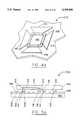
- FIGS. 1a and 1bshow such an assembly 630, which combines chip-on-board technology and flip chip technology into a "brickwork" assembly.
- FIG. 1ashows two integrated circuit dies 634a and 634b mounted to a substrate 632 and wire bonded with bond wires 638 to conductive traces on the substrate (not shown, to reduce illustrative clutter). Dies 634a and 634b are spaced closely enough that a third "flip-chip" die 636 may span the gap between them. Two sets of contact areas on the underside (circuit side) of die 636 mate with and connect to matching contact areas on dies 634a and 634b.
- FIG. 1ashows two integrated circuit dies 634a and 634b mounted to a substrate 632 and wire bonded with bond wires 638 to conductive traces on the substrate (not shown, to reduce illustrative clutter). Dies 634a and 634b are spaced closely enough that a third "flip-chip" die 636 may span the gap between
- 1bis a cross-sectional view of a portion of the assembly 630 showing bump contact areas 636a and 636b on the underside (circuit side) of die 636 and mating contact areas 635a and 635b on dies 634a and 634b, respectively.
- this assembly 630does make use of bond wires 638 for connection to conductive traces on the substrate, it has the advantage that conventional, single-sided flip-chip dies may be used for all of the dies in the assembly.
- the face-to-face overlap between the die 636 and either of the dies 634a or 634bis preferably limited to just enough to make contact between the dies. In this manner, overlap of the active circuit elements occupying a substantial central portion of the respective dies is substantially avoided, and heat can be efficiently dissipated from the individual dies.
- FIG. 6illustrates a two-tier flip-chip assembly 700 used to increase the bond pad density (by increasing the amount of "aggregate" die periphery available) for a given footprint (area of the assembly as seen in plan view).
- a semiconductor die 720is flip-chip mounted to another semiconductor die 710. This involves bond sites around the periphery of the bottom of the die 720, and bond sites in a corresponding (central) area of the die 710. The techniques discussed hereinabove are suitably employed to make the die-to-die connections.
- a peripheral area 718is defined along (within) the edges 716 (one indicated) of the die 710 between the edges 716 and a dashed line 717 representing a boundary between the peripheral area 718 and an active element area 715.
- the peripheral area 718is limited by its size to holding only a limited first number "n" of bond pads (for I/O connections to the die 710).
- Another peripheral area 728is defined along edges 726 (one indicated) of the die 720 between the edges 726 and a dashed line 727 representing a boundary between the peripheral area 728 and an active element area 725.
- the peripheral area 728is similarly limited by its size to holding only a limited second number "m" of bond pads (for I/O connections to the die 720).
- the "footprint" area of the assembly 700 of dies 710, 720is defined as the plan area of the larger die 710.
- the die 710is a square die, having side edges measuring one unit.
- the footprint area for the assembly 700is one unit 2 .
- the periphery to area ratio for a square shapeis 4:1.
- the square die 710has 4 units of peripheral area available for I/O.
- the die 720is a square die, having a 4:1 ratio of periphery (peripheral area) to overall area.
- the periphery to footprint area ratio for the assembly 700is, in aggregate 6:1, which represents a 50% improvement over the periphery:area ratio for the die 710.
- the periphery to footprint area ratio for the assemblyis 7:1, without exceeding the footprint of die 710.
- the extreme aspect ratios of a greatly elongated rectangular die (7:1 or 10:1) having comparable periphery:areawould preclude the use of standard packaging techniques.
- the flip-chip arrangement of FIG. 6provides a significant increase in the amount of I/O (peripheral area) on the assembly while simultaneously providing greater circuit area within the footprint of the die 710.
- bond pads for making external connections to a semiconductor die or die assemblyare generally disposed along the die edges, an increase in die periphery to footprint area ratio signals an increase in potential bond pad density, since more space is available for bond pads.
- I/O counts on the order of in excess of six hundrede.g., >600, 650, >700, >800, >900, >1000 (can readily be achieved using "standard” die sizes (on the order of a few centimeters) and "standard” packages.
- m+n bond pads (I/O)is readily achieved in the example of FIG. 6.
- the technique described hereinaboveprovides for dramatic increases in the I/O (periphery) available within a given assembly footprint, providing periphery to footprint area ratios of greater than "x":1, where "x" is, for example, 5.0, 5.25, 5.5, 5.75, 6.0, 6.25, 6.5, 6.75, or 7.0.
- An upper bound for the periphery to area ratio expansion provided by this techniqueis twice the periphery to area ratio of the footprint, although this is only achieved by using two dies of the same size, which would make connection to the bottom-most die extremely cumbersome or impossible.
- Other die shapesmay be used, such as, rectangles, triangles, trapezoids, parallelograms, etc., with similar increases in periphery to footprint area ratio.
- Multi-tier flip-chip assembliesmay also be used to further increase the periphery to footprint area ratio (i.e., in excess of twice that of the largest die).
- FIG. 6While the foregoing discussion with respect to FIG. 6 has been directed generally toward a single die (e.g., 720) atop another die (e.g., 710), it will be appreciated by one of ordinary skill in the art that more than one die can be "flipped" onto another die, yielding similar increases in die periphery to footprint area ratio.
- Double-sided flip-chip diesare particularly useful in configurations such as that shown in FIG. 6 for permitting interconnections between the upward-facing side of the bottom die (e.g., 710) and the downward-facing side of the top die (e.g., 720), while still permitting bond pads (I/O) to be disposed along the periphery of the upward-facing side of the top-die. Examples of such configurations are shown in FIGS. 7a and 7b.
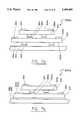
- FIG. 7ais a side view of a stacked flip-chip die assembly 800a using double-sided flip-chip dies which increases the number of bond pads (die periphery area) available within a given footprint.
- a first double-sided flip-chip die 820is mounted to conductive pads 840 on a substrate 810a via solder bump contacts 842 on a downward facing (as viewed in the Figure) surface 820b of the die 820.
- Bond pads 850for external connections, are disposed on an upward facing (as shown) surface 820a of the die 820 along the edges (periphery) thereof.
- a second double sided flip-chip die 830is mounted to bond pads 860 disposed on the top surface 820a of the first die 820 via bump contacts 862 disposed on a downward facing surface of the second die 830.
- An upward facing surface of the second die 820has bond pads 854, for external connections, disposed along the edges (periphery) thereof.
- the substrate 810ais typically part of a semiconductor package, but can also be a printed circuit board.
- FIG. 7bis a side view of another stacked flip-chip die assembly 800b which increases the number of bond pads (die periphery area) available within a given footprint, using the same second die 830 as shown with respect to FIG. 7a.
- a first die 870is bonded with an adhesive 880 to a substrate 810b.
- An upward facing side 870a of the substratehas bond pads 850a disposed along the edges thereof, for the purpose of making external connections to the die 870.
- the die 830is mounted to second bond pads 860a disposed on the upward facing surface 870a of the first die 870 via bump contacts 862 disposed on the downward facing surface 830b of the second die 830.
- bond pads 854, disposed on the top surface 830a of the second die 830are also available for external connections.
- FIGS. 7a and 7bshow a single die disposed atop another (i.e., die-on-die), it is within the scope of the present invention to dispose more than one die atop another (i.e., dies-on die), providing similar increases in bond pad density for a given footprint area.
- FIGS. 6, 7a and 7bPotential applications for assemblies such as those discussed hereinabove with respect to FIGS. 6, 7a and 7b include flip-chip mounting of logic chips (dies) to a large memory die, and providing additional external connections via the flip-chip mounted logic chips (dies).
- logic chipsdies
- one or more logic diescan be flipped onto the surface of a rectangular memory die.
Landscapes
- Engineering & Computer Science (AREA)
- Computer Hardware Design (AREA)
- Microelectronics & Electronic Packaging (AREA)
- Power Engineering (AREA)
- Physics & Mathematics (AREA)
- General Physics & Mathematics (AREA)
- Condensed Matter Physics & Semiconductors (AREA)
- Theoretical Computer Science (AREA)
- Architecture (AREA)
- Evolutionary Computation (AREA)
- Geometry (AREA)
- General Engineering & Computer Science (AREA)
- Wire Bonding (AREA)
Abstract
Description
Claims (8)
Priority Applications (3)
| Application Number | Priority Date | Filing Date | Title |
|---|---|---|---|
| US07/975,185US5399898A (en) | 1992-07-17 | 1992-11-12 | Multi-chip semiconductor arrangements using flip chip dies |
| US08/105,547US5504035A (en) | 1989-08-28 | 1993-08-12 | Process for solder ball interconnecting a semiconductor device to a substrate using a noble metal foil embedded interposer substrate |
| US08/428,323US5569963A (en) | 1989-08-28 | 1995-04-25 | Preformed planar structures for semiconductor device assemblies |
Applications Claiming Priority (3)
| Application Number | Priority Date | Filing Date | Title |
|---|---|---|---|
| US07/916,328US5340772A (en) | 1992-07-17 | 1992-07-17 | Method of increasing the layout efficiency of dies on a wafer and increasing the ratio of I/O area to active area per die |
| US07/935,449US5300815A (en) | 1992-07-17 | 1992-08-25 | Technique of increasing bond pad density on a semiconductor die |
| US07/975,185US5399898A (en) | 1992-07-17 | 1992-11-12 | Multi-chip semiconductor arrangements using flip chip dies |
Related Parent Applications (2)
| Application Number | Title | Priority Date | Filing Date |
|---|---|---|---|
| US07/916,328Continuation-In-PartUS5340772A (en) | 1992-07-17 | 1992-07-17 | Method of increasing the layout efficiency of dies on a wafer and increasing the ratio of I/O area to active area per die |
| US07/935,449Continuation-In-PartUS5300815A (en) | 1992-07-17 | 1992-08-25 | Technique of increasing bond pad density on a semiconductor die |
Related Child Applications (2)
| Application Number | Title | Priority Date | Filing Date |
|---|---|---|---|
| US40057289AContinuation | 1989-08-28 | 1989-08-28 | |
| US08/105,547Continuation-In-PartUS5504035A (en) | 1989-08-28 | 1993-08-12 | Process for solder ball interconnecting a semiconductor device to a substrate using a noble metal foil embedded interposer substrate |
Publications (1)
| Publication Number | Publication Date |
|---|---|
| US5399898Atrue US5399898A (en) | 1995-03-21 |
Family
ID=27129690
Family Applications (1)
| Application Number | Title | Priority Date | Filing Date |
|---|---|---|---|
| US07/975,185Expired - LifetimeUS5399898A (en) | 1989-08-28 | 1992-11-12 | Multi-chip semiconductor arrangements using flip chip dies |
Country Status (1)
| Country | Link |
|---|---|
| US (1) | US5399898A (en) |
Cited By (316)
| Publication number | Priority date | Publication date | Assignee | Title |
|---|---|---|---|---|
| US5498905A (en)* | 1994-08-26 | 1996-03-12 | Hughes Aircraft Company | Layered features for co-fired module integration |
| WO1996030932A3 (en)* | 1995-02-06 | 1996-11-21 | Grumman Aerospace Corp | Microcircuit via interconnect |
| US5677567A (en)* | 1996-06-17 | 1997-10-14 | Micron Technology, Inc. | Leads between chips assembly |
| US5696031A (en)* | 1996-11-20 | 1997-12-09 | Micron Technology, Inc. | Device and method for stacking wire-bonded integrated circuit dice on flip-chip bonded integrated circuit dice |
| US5715144A (en)* | 1994-12-30 | 1998-02-03 | International Business Machines Corporation | Multi-layer, multi-chip pyramid and circuit board structure |
| US5742086A (en)* | 1994-11-02 | 1998-04-21 | Lsi Logic Corporation | Hexagonal DRAM array |
| US5760478A (en)* | 1996-08-20 | 1998-06-02 | International Business Machines Corporation | Clock skew minimization system and method for integrated circuits |
| US5773882A (en)* | 1994-04-28 | 1998-06-30 | Kabushiki Kaisha Toshiba | Seminconductor package |
| US5777360A (en)* | 1994-11-02 | 1998-07-07 | Lsi Logic Corporation | Hexagonal field programmable gate array architecture |
| US5783870A (en)* | 1995-03-16 | 1998-07-21 | National Semiconductor Corporation | Method for connecting packages of a stacked ball grid array structure |
| US5789770A (en)* | 1994-11-02 | 1998-08-04 | Lsi Logic Corporation | Hexagonal architecture with triangular shaped cells |
| US5801422A (en)* | 1994-11-02 | 1998-09-01 | Lsi Logic Corporation | Hexagonal SRAM architecture |
| US5801448A (en)* | 1996-05-20 | 1998-09-01 | Micron Technology, Inc. | Conductive lines on the back side of wafers and dice for semiconductor interconnects |
| US5808330A (en)* | 1994-11-02 | 1998-09-15 | Lsi Logic Corporation | Polydirectional non-orthoginal three layer interconnect architecture |
| US5811863A (en)* | 1994-11-02 | 1998-09-22 | Lsi Logic Corporation | Transistors having dynamically adjustable characteristics |
| US5822214A (en)* | 1994-11-02 | 1998-10-13 | Lsi Logic Corporation | CAD for hexagonal architecture |
| US5834821A (en)* | 1994-11-02 | 1998-11-10 | Lsi Logic Corporation | Triangular semiconductor "AND" gate device |
| US5864165A (en)* | 1994-11-02 | 1999-01-26 | Lsi Logic Corporation | Triangular semiconductor NAND gate |
| US5872380A (en)* | 1994-11-02 | 1999-02-16 | Lsi Logic Corporation | Hexagonal sense cell architecture |
| US5889329A (en)* | 1994-11-02 | 1999-03-30 | Lsi Logic Corporation | Tri-directional interconnect architecture for SRAM |
| US5889327A (en)* | 1996-10-04 | 1999-03-30 | Mitsubishi Denki Kabushiki Kaisha | Semiconductor device with a package having a plurality of bump electrodes and module with a plurality of semiconductor devices |
| US5907769A (en)* | 1996-12-30 | 1999-05-25 | Micron Technology, Inc. | Leads under chip in conventional IC package |
| US5907903A (en)* | 1996-05-24 | 1999-06-01 | International Business Machines Corporation | Multi-layer-multi-chip pyramid and circuit board structure and method of forming same |
| US5914535A (en)* | 1997-02-10 | 1999-06-22 | Delco Electronics Corporation | Flip chip-on-flip chip multi-chip module |
| US5917242A (en)* | 1996-05-20 | 1999-06-29 | Micron Technology, Inc. | Combination of semiconductor interconnect |
| US5939777A (en)* | 1996-12-06 | 1999-08-17 | Texas Instruments Incorporated | High aspect ratio integrated circuit chip and method for producing the same |
| US5952725A (en)* | 1996-02-20 | 1999-09-14 | Micron Technology, Inc. | Stacked semiconductor devices |
| US5952712A (en)* | 1996-07-18 | 1999-09-14 | Nec Corporation | Packaged semiconductor device and method of manufacturing the same |
| US5973376A (en)* | 1994-11-02 | 1999-10-26 | Lsi Logic Corporation | Architecture having diamond shaped or parallelogram shaped cells |
| US5977640A (en)* | 1998-06-26 | 1999-11-02 | International Business Machines Corporation | Highly integrated chip-on-chip packaging |
| US6002177A (en)* | 1995-12-27 | 1999-12-14 | International Business Machines Corporation | High density integrated circuit packaging with chip stacking and via interconnections |
| US6005778A (en)* | 1995-06-15 | 1999-12-21 | Honeywell Inc. | Chip stacking and capacitor mounting arrangement including spacers |
| US6097073A (en)* | 1994-11-02 | 2000-08-01 | Lsi Logic Corporation | Triangular semiconductor or gate |
| US6096576A (en)* | 1997-09-02 | 2000-08-01 | Silicon Light Machines | Method of producing an electrical interface to an integrated circuit device having high density I/O count |
| US6122187A (en)* | 1998-11-23 | 2000-09-19 | Micron Technology, Inc. | Stacked integrated circuits |
| US6150726A (en)* | 1996-09-06 | 2000-11-21 | International Business Machines Corp. | Component carrier with raised bonding sites |
| US6166444A (en)* | 1999-06-21 | 2000-12-26 | United Microelectronics Corp. | Cascade-type chip module |
| US6168971B1 (en) | 1998-05-05 | 2001-01-02 | Fujitsu Limited | Method of assembling thin film jumper connectors to a substrate |
| US6184060B1 (en) | 1996-10-29 | 2001-02-06 | Trusi Technologies Llc | Integrated circuits and methods for their fabrication |
| US6201301B1 (en) | 1998-01-21 | 2001-03-13 | Lsi Logic Corporation | Low cost thermally enhanced flip chip BGA |
| US6207476B1 (en)* | 1999-06-10 | 2001-03-27 | Vlsi Technology, Inc. | Methods of packaging an integrated circuit and methods of forming an integrated circuit package |
| US6225699B1 (en) | 1998-06-26 | 2001-05-01 | International Business Machines Corporation | Chip-on-chip interconnections of varied characteristics |
| US6229219B1 (en)* | 2000-03-29 | 2001-05-08 | Advanced Micro Devices, Inc. | Flip chip package compatible with multiple die footprints and method of assembling the same |
| US6232667B1 (en) | 1999-06-29 | 2001-05-15 | International Business Machines Corporation | Technique for underfilling stacked chips on a cavity MLC module |
| US6249136B1 (en)* | 1999-06-28 | 2001-06-19 | Advanced Micro Devices, Inc. | Bottom side C4 bumps for integrated circuits |
| US6261865B1 (en) | 1998-10-06 | 2001-07-17 | Micron Technology, Inc. | Multi chip semiconductor package and method of construction |
| US6278181B1 (en)* | 1999-06-28 | 2001-08-21 | Advanced Micro Devices, Inc. | Stacked multi-chip modules using C4 interconnect technology having improved thermal management |
| WO2001080317A1 (en)* | 2000-04-19 | 2001-10-25 | Infineon Technologies Ag | Semiconductor component comprising several semiconductor chips |
| US6319752B1 (en)* | 2000-04-24 | 2001-11-20 | Advanced Micro Devices, Inc. | Single-layer autorouter |
| US6322903B1 (en) | 1999-12-06 | 2001-11-27 | Tru-Si Technologies, Inc. | Package of integrated circuits and vertical integration |
| US6383837B1 (en)* | 1997-04-25 | 2002-05-07 | Kabushiki Kaisha Toshiba | Method of manufacturing a multi-chip semiconductor device effective to improve alignment |
| US6407434B1 (en) | 1994-11-02 | 2002-06-18 | Lsi Logic Corporation | Hexagonal architecture |
| US6407456B1 (en) | 1996-02-20 | 2002-06-18 | Micron Technology, Inc. | Multi-chip device utilizing a flip chip and wire bond assembly |
| US6406940B1 (en)* | 2000-08-14 | 2002-06-18 | Intermedics Inc. | Method and apparatus for stacking IC devices |
| US20020076854A1 (en)* | 2000-12-15 | 2002-06-20 | Pierce John L. | System, method and apparatus for constructing a semiconductor wafer-interposer using B-Stage laminates |
| US20020078401A1 (en)* | 2000-12-15 | 2002-06-20 | Fry Michael Andrew | Test coverage analysis system |
| US6414391B1 (en) | 1998-06-30 | 2002-07-02 | Micron Technology, Inc. | Module assembly for stacked BGA packages with a common bus bar in the assembly |
| US20020084513A1 (en)* | 1996-10-29 | 2002-07-04 | Oleg Siniaguine | Integrated circuits and methods for their fabrication |
| US6424034B1 (en) | 1998-08-31 | 2002-07-23 | Micron Technology, Inc. | High performance packaging for microprocessors and DRAM chips which minimizes timing skews |
| US20020097063A1 (en)* | 1999-11-16 | 2002-07-25 | Kline Jerry D. | Wafer level interposer |
| US20020109133A1 (en)* | 1999-02-23 | 2002-08-15 | Junichi Hikita | Semiconductor chip and semiconductor device using the same, and method of fabricating semiconductor chip |
| US20020119600A1 (en)* | 2001-02-23 | 2002-08-29 | Micro-Asi, Inc. | Wafer-interposer using a ceramic substrate |
| US6461956B1 (en)* | 1999-03-01 | 2002-10-08 | United Microelectronics Corp. | Method of forming package |
| US20020195697A1 (en)* | 2001-06-21 | 2002-12-26 | Mess Leonard E. | Stacked mass storage flash memory package |
| US20030022430A1 (en)* | 2001-07-24 | 2003-01-30 | Motorola, Inc. | Structure and method for fabricating configurable transistor devices utilizing the formation of a compliant substrate for materials used to form the same |
| US6515370B2 (en) | 1997-03-10 | 2003-02-04 | Seiko Epson Corporation | Electronic component and semiconductor device, method for manufacturing the same, circuit board have the same mounted thereon, and electronic equipment having the circuit board |
| US20030036217A1 (en)* | 2001-08-16 | 2003-02-20 | Motorola, Inc. | Microcavity semiconductor laser coupled to a waveguide |
| US20030038356A1 (en)* | 2001-08-24 | 2003-02-27 | Derderian James M | Semiconductor devices including stacking spacers thereon, assemblies including the semiconductor devices, and methods |
| US20030038157A1 (en)* | 2001-07-25 | 2003-02-27 | Uta Gebauer | Electronic component with a semiconductor chip and method for producing the electronic component |
| US6531782B1 (en) | 2001-06-19 | 2003-03-11 | Cypress Semiconductor Corp. | Method of placing die to minimize die-to-die routing complexity on a substrate |
| US6536882B1 (en) | 2000-07-26 | 2003-03-25 | Eastman Kodak Company | Inkjet printhead having substrate feedthroughs for accommodating conductors |
| US20030061590A1 (en)* | 2001-09-26 | 2003-03-27 | Boggs David W. | System and method for printed circuit board conductor channeling |
| US6552425B1 (en) | 1998-12-18 | 2003-04-22 | Intel Corporation | Integrated circuit package |
| US6577002B1 (en)* | 2001-11-29 | 2003-06-10 | Sun Microsystems, Inc. | 180 degree bump placement layout for an integrated circuit power grid |
| US6583502B2 (en) | 2001-04-17 | 2003-06-24 | Micron Technology, Inc. | Apparatus for package reduction in stacked chip and board assemblies |
| DE10161043A1 (en)* | 2001-12-12 | 2003-07-03 | Infineon Technologies Ag | chip system |
| US6589856B2 (en) | 2001-08-06 | 2003-07-08 | Motorola, Inc. | Method and apparatus for controlling anti-phase domains in semiconductor structures and devices |
| US20030129775A1 (en)* | 2000-07-31 | 2003-07-10 | Kline Jerry D. | Matched set of integrated circuit chips selected from a multi wafer interposer |
| US20030128044A1 (en)* | 2000-12-15 | 2003-07-10 | Pierce John L. | Method for producing a wafer interposer for use in a wafer interposer assembly |
| US20030127720A1 (en)* | 2002-01-07 | 2003-07-10 | Jen-Kuang Fang | Multi-chip stack package and fabricating method thereof |
| US20030148613A1 (en)* | 1997-08-22 | 2003-08-07 | Ahn Kie Y. | Wireless communications system and method of making |
| US20030148108A1 (en)* | 2000-12-15 | 2003-08-07 | Pierce John L. | Wafer interposer assembly and system for building same |
| US20030161511A1 (en)* | 2000-06-09 | 2003-08-28 | Ovidiu Vermesan | Measuring instrument and method for optical measurement of velocity and direction of particles |
| US20030161512A1 (en)* | 2000-06-09 | 2003-08-28 | Svein Mathiassen | Sensor unit, especially for fingerprint sensors |
| US6624506B2 (en)* | 2000-04-20 | 2003-09-23 | Kabushiki Kaisha Toshiba | Multichip semiconductor device and memory card |
| US20030186486A1 (en)* | 2002-03-28 | 2003-10-02 | Swan Johanna M. | Integrated circuit die and an electronic assembly having a three-dimensional interconnection scheme |
| US20030183943A1 (en)* | 2002-03-28 | 2003-10-02 | Swan Johanna M. | Integrated circuit die and an electronic assembly having a three-dimensional interconnection scheme |
| US6630631B1 (en)* | 2002-03-27 | 2003-10-07 | Intel Corporation | Apparatus and method for interconnection between a component and a printed circuit board |
| US6635970B2 (en) | 2002-02-06 | 2003-10-21 | International Business Machines Corporation | Power distribution design method for stacked flip-chip packages |
| US6638838B1 (en) | 2000-10-02 | 2003-10-28 | Motorola, Inc. | Semiconductor structure including a partially annealed layer and method of forming the same |
| US6639249B2 (en) | 2001-08-06 | 2003-10-28 | Motorola, Inc. | Structure and method for fabrication for a solid-state lighting device |
| US20030207589A1 (en)* | 2002-05-03 | 2003-11-06 | Thoughtbeam, Inc. | Method for growing a monocrystalline oxide layer and for fabricating a semiconductor device on a monocrystalline substrate |
| US6646293B2 (en) | 2001-07-18 | 2003-11-11 | Motorola, Inc. | Structure for fabricating high electron mobility transistors utilizing the formation of complaint substrates |
| US6650009B2 (en)* | 2000-07-18 | 2003-11-18 | Siliconware Precision Industries Co., Ltd. | Structure of a multi chip module having stacked chips |
| US20030214234A1 (en)* | 2002-05-20 | 2003-11-20 | Ushiodenki Kabushiki Kaisha | Discharge lamp |
| US6664628B2 (en)* | 1998-07-13 | 2003-12-16 | Formfactor, Inc. | Electronic component overlapping dice of unsingulated semiconductor wafer |
| US6667196B2 (en) | 2001-07-25 | 2003-12-23 | Motorola, Inc. | Method for real-time monitoring and controlling perovskite oxide film growth and semiconductor structure formed using the method |
| US6673667B2 (en) | 2001-08-15 | 2004-01-06 | Motorola, Inc. | Method for manufacturing a substantially integral monolithic apparatus including a plurality of semiconductor materials |
| US6673646B2 (en) | 2001-02-28 | 2004-01-06 | Motorola, Inc. | Growth of compound semiconductor structures on patterned oxide films and process for fabricating same |
| US20040012037A1 (en)* | 2002-07-18 | 2004-01-22 | Motorola, Inc. | Hetero-integration of semiconductor materials on silicon |
| US6683384B1 (en)* | 1997-10-08 | 2004-01-27 | Agere Systems Inc | Air isolated crossovers |
| US6686657B1 (en) | 2000-11-07 | 2004-02-03 | Eaglestone Partners I, Llc | Interposer for improved handling of semiconductor wafers and method of use of same |
| US20040026122A1 (en)* | 2001-04-06 | 2004-02-12 | Katsuhiko Hayashi | Printed circuit board and production method therefor, and laminated printed circuit board |
| US6693298B2 (en) | 2001-07-20 | 2004-02-17 | Motorola, Inc. | Structure and method for fabricating epitaxial semiconductor on insulator (SOI) structures and devices utilizing the formation of a compliant substrate for materials used to form same |
| US6693033B2 (en) | 2000-02-10 | 2004-02-17 | Motorola, Inc. | Method of removing an amorphous oxide from a monocrystalline surface |
| US20040046264A1 (en)* | 2002-09-09 | 2004-03-11 | Ho Kwun Yao | High density integrated circuit packages and method for the same |
| US6706557B2 (en) | 2001-09-21 | 2004-03-16 | Micron Technology, Inc. | Method of fabricating stacked die configurations utilizing redistribution bond pads |
| US6707591B2 (en) | 2001-04-10 | 2004-03-16 | Silicon Light Machines | Angled illumination for a single order light modulator based projection system |
| US6709989B2 (en) | 2001-06-21 | 2004-03-23 | Motorola, Inc. | Method for fabricating a semiconductor structure including a metal oxide interface with silicon |
| US6712480B1 (en) | 2002-09-27 | 2004-03-30 | Silicon Light Machines | Controlled curvature of stressed micro-structures |
| US6714337B1 (en) | 2002-06-28 | 2004-03-30 | Silicon Light Machines | Method and device for modulating a light beam and having an improved gamma response |
| US6717254B2 (en) | 2001-02-22 | 2004-04-06 | Tru-Si Technologies, Inc. | Devices having substrates with opening passing through the substrates and conductors in the openings, and methods of manufacture |
| US20040070312A1 (en)* | 2002-10-10 | 2004-04-15 | Motorola, Inc. | Integrated circuit and process for fabricating the same |
| US6728023B1 (en) | 2002-05-28 | 2004-04-27 | Silicon Light Machines | Optical device arrays with optimized image resolution |
| US20040092179A1 (en)* | 2002-11-12 | 2004-05-13 | O'rourke Maurice C. | Reset speed control for watercraft |
| US6747781B2 (en) | 2001-06-25 | 2004-06-08 | Silicon Light Machines, Inc. | Method, apparatus, and diffuser for reducing laser speckle |
| US6753205B2 (en) | 2001-09-13 | 2004-06-22 | Tru-Si Technologies, Inc. | Method for manufacturing a structure comprising a substrate with a cavity and a semiconductor integrated circuit bonded to a contact pad located in the cavity |
| US6764875B2 (en) | 1998-07-29 | 2004-07-20 | Silicon Light Machines | Method of and apparatus for sealing an hermetic lid to a semiconductor die |
| US6767751B2 (en) | 2002-05-28 | 2004-07-27 | Silicon Light Machines, Inc. | Integrated driver process flow |
| US20040150003A1 (en)* | 2000-02-10 | 2004-08-05 | Motorola, Inc. | Semiconductor structure, semiconductor device, communicating device, integrated circuit, and process for fabricating the same |
| US20040151463A1 (en)* | 2003-02-03 | 2004-08-05 | Motorola, Inc. | Optical waveguide structure and method for fabricating the same |
| US20040150043A1 (en)* | 2003-02-03 | 2004-08-05 | Motorola, Inc. | Structure and method for fabricating semiconductor microresonator devices |
| US20040155328A1 (en)* | 2000-07-31 | 2004-08-12 | Kline Jerry D. | Wafer-interposer assembly |
| US6782205B2 (en) | 2001-06-25 | 2004-08-24 | Silicon Light Machines | Method and apparatus for dynamic equalization in wavelength division multiplexing |
| US20040164315A1 (en)* | 2003-02-25 | 2004-08-26 | Motorola, Inc. | Structure and device including a tunneling piezoelectric switch and method of forming same |
| US6784023B2 (en) | 1996-05-20 | 2004-08-31 | Micron Technology, Inc. | Method of fabrication of stacked semiconductor devices |
| US6794750B2 (en)* | 1997-12-26 | 2004-09-21 | Nec Electronics Corporation | Semiconductor device |
| US20040188819A1 (en)* | 2003-03-31 | 2004-09-30 | Farnworth Warren M. | Wafer level methods for fabricating multi-dice chip scale semiconductor components |
| US6801354B1 (en) | 2002-08-20 | 2004-10-05 | Silicon Light Machines, Inc. | 2-D diffraction grating for substantially eliminating polarization dependent losses |
| US6800238B1 (en) | 2002-01-15 | 2004-10-05 | Silicon Light Machines, Inc. | Method for domain patterning in low coercive field ferroelectrics |
| US6806578B2 (en)* | 2000-03-16 | 2004-10-19 | International Business Machines Corporation | Copper pad structure |
| US6806997B1 (en) | 2003-02-28 | 2004-10-19 | Silicon Light Machines, Inc. | Patterned diffractive light modulator ribbon for PDL reduction |
| US6809421B1 (en)* | 1996-12-02 | 2004-10-26 | Kabushiki Kaisha Toshiba | Multichip semiconductor device, chip therefor and method of formation thereof |
| US6813059B2 (en) | 2002-06-28 | 2004-11-02 | Silicon Light Machines, Inc. | Reduced formation of asperities in contact micro-structures |
| US20040217444A1 (en)* | 2001-10-17 | 2004-11-04 | Motorola, Inc. | Method and apparatus utilizing monocrystalline insulator |
| US6815712B1 (en) | 2000-10-02 | 2004-11-09 | Eaglestone Partners I, Llc | Method for selecting components for a matched set from a wafer-interposer assembly |
| US6822469B1 (en) | 2000-07-31 | 2004-11-23 | Eaglestone Partners I, Llc | Method for testing multiple semiconductor wafers |
| US6822797B1 (en) | 2002-05-31 | 2004-11-23 | Silicon Light Machines, Inc. | Light modulator structure for producing high-contrast operation using zero-order light |
| US20040232431A1 (en)* | 2001-07-16 | 2004-11-25 | Motorola, Inc. | Semiconductor structure and method for implementing cross-point switch functionality |
| US6829092B2 (en) | 2001-08-15 | 2004-12-07 | Silicon Light Machines, Inc. | Blazed grating light valve |
| US6829258B1 (en) | 2002-06-26 | 2004-12-07 | Silicon Light Machines, Inc. | Rapidly tunable external cavity laser |
| US6829077B1 (en) | 2003-02-28 | 2004-12-07 | Silicon Light Machines, Inc. | Diffractive light modulator with dynamically rotatable diffraction plane |
| US20040245649A1 (en)* | 2003-04-16 | 2004-12-09 | Seiko Epson Corporation | Optical device, optical module, semiconductor apparatus and its manufacturing method, and electronic apparatus |
| US20050012189A1 (en)* | 2002-08-16 | 2005-01-20 | Ho Kwun Yao | Integrated circuit package with a balanced-part structure |
| US6848177B2 (en) | 2002-03-28 | 2005-02-01 | Intel Corporation | Integrated circuit die and an electronic assembly having a three-dimensional interconnection scheme |
| US6865346B1 (en) | 2001-06-05 | 2005-03-08 | Silicon Light Machines Corporation | Fiber optic transceiver |
| US20050056210A1 (en)* | 2000-07-24 | 2005-03-17 | Motorola | Heterojunction tunneling diodes and process for fabricating same |
| US6872984B1 (en) | 1998-07-29 | 2005-03-29 | Silicon Light Machines Corporation | Method of sealing a hermetic lid to a semiconductor die at an angle |
| US6885065B2 (en) | 2002-11-20 | 2005-04-26 | Freescale Semiconductor, Inc. | Ferromagnetic semiconductor structure and method for forming the same |
| US20050088900A1 (en)* | 1998-09-25 | 2005-04-28 | Chan Tsiu C. | Stacked multi-component integrated circuit microprocessor |
| US20050121765A1 (en)* | 2003-12-09 | 2005-06-09 | Advanced Semiconductor Engineering, Inc. | Multi-chips bumpless assembly package and manufacturing method thereof |
| US6908201B2 (en) | 2002-06-28 | 2005-06-21 | Silicon Light Machines Corporation | Micro-support structures |
| US6922272B1 (en) | 2003-02-14 | 2005-07-26 | Silicon Light Machines Corporation | Method and apparatus for leveling thermal stress variations in multi-layer MEMS devices |
| US6922273B1 (en) | 2003-02-28 | 2005-07-26 | Silicon Light Machines Corporation | PDL mitigation structure for diffractive MEMS and gratings |
| US20050167798A1 (en)* | 2004-01-29 | 2005-08-04 | Doan Trung T. | Die-wafer package and method of fabricating same |
| US6927891B1 (en) | 2002-12-23 | 2005-08-09 | Silicon Light Machines Corporation | Tilt-able grating plane for improved crosstalk in 1×N blaze switches |
| US6928207B1 (en) | 2002-12-12 | 2005-08-09 | Silicon Light Machines Corporation | Apparatus for selectively blocking WDM channels |
| US6934070B1 (en) | 2002-12-18 | 2005-08-23 | Silicon Light Machines Corporation | Chirped optical MEM device |
| US20050189632A1 (en)* | 2004-03-01 | 2005-09-01 | Patrick Morrow | Sealed three dimensional metal bonded integrated circuits |
| US20050194593A1 (en)* | 2001-01-19 | 2005-09-08 | Freescale Semiconductor, Inc. | Structure and method for fabricating GaN devices utilizing the formation of a compliant substrate |
| US6947613B1 (en) | 2003-02-11 | 2005-09-20 | Silicon Light Machines Corporation | Wavelength selective switch and equalizer |
| US6956878B1 (en) | 2000-02-07 | 2005-10-18 | Silicon Light Machines Corporation | Method and apparatus for reducing laser speckle using polarization averaging |
| US6956995B1 (en) | 2001-11-09 | 2005-10-18 | Silicon Light Machines Corporation | Optical communication arrangement |
| US20050230682A1 (en)* | 2004-04-16 | 2005-10-20 | Seiko Epson Corporation | Thin film device, integrated circuit, electrooptic device, and electronic device |
| US6979904B2 (en)* | 2002-04-19 | 2005-12-27 | Micron Technology, Inc. | Integrated circuit package having reduced interconnects |
| US6987600B1 (en) | 2002-12-17 | 2006-01-17 | Silicon Light Machines Corporation | Arbitrary phase profile for better equalization in dynamic gain equalizer |
| US6992321B2 (en) | 2001-07-13 | 2006-01-31 | Motorola, Inc. | Structure and method for fabricating semiconductor structures and devices utilizing piezoelectric materials |
| US6991953B1 (en) | 2001-09-13 | 2006-01-31 | Silicon Light Machines Corporation | Microelectronic mechanical system and methods |
| US7005717B2 (en) | 2000-05-31 | 2006-02-28 | Freescale Semiconductor, Inc. | Semiconductor device and method |
| US7019332B2 (en) | 2001-07-20 | 2006-03-28 | Freescale Semiconductor, Inc. | Fabrication of a wavelength locker within a semiconductor structure |
| US20060071342A1 (en)* | 2004-09-29 | 2006-04-06 | Sanyo Electric Co., Ltd. | Semiconductor device manufacturing method of the same |
| US20060073632A1 (en)* | 2004-10-06 | 2006-04-06 | Garcia Jason A | Die handling system |
| US7027202B1 (en) | 2003-02-28 | 2006-04-11 | Silicon Light Machines Corp | Silicon substrate as a light modulator sacrificial layer |
| US7042611B1 (en) | 2003-03-03 | 2006-05-09 | Silicon Light Machines Corporation | Pre-deflected bias ribbons |
| US7045815B2 (en) | 2001-04-02 | 2006-05-16 | Freescale Semiconductor, Inc. | Semiconductor structure exhibiting reduced leakage current and method of fabricating same |
| US7054515B1 (en) | 2002-05-30 | 2006-05-30 | Silicon Light Machines Corporation | Diffractive light modulator-based dynamic equalizer with integrated spectral monitor |
| US20060113656A1 (en)* | 2004-11-30 | 2006-06-01 | Uang Rouh H | Composite conductive film and semiconductor package using such film |
| US7057795B2 (en) | 2002-08-20 | 2006-06-06 | Silicon Light Machines Corporation | Micro-structures with individually addressable ribbon pairs |
| US7057819B1 (en) | 2002-12-17 | 2006-06-06 | Silicon Light Machines Corporation | High contrast tilting ribbon blazed grating |
| US7061102B2 (en) | 2001-06-11 | 2006-06-13 | Xilinx, Inc. | High performance flipchip package that incorporates heat removal with minimal thermal mismatch |
| US7068372B1 (en) | 2003-01-28 | 2006-06-27 | Silicon Light Machines Corporation | MEMS interferometer-based reconfigurable optical add-and-drop multiplexor |
| US20060138649A1 (en)* | 2002-10-08 | 2006-06-29 | Chippac, Inc. | Semiconductor multi-package module having inverted second package stacked over die-up flip-chip ball grid array (BGA) package |
| US7098542B1 (en)* | 2003-11-07 | 2006-08-29 | Xilinx, Inc. | Multi-chip configuration to connect flip-chips to flip-chips |
| US20060261471A1 (en)* | 2005-05-20 | 2006-11-23 | Nec Electronics Corporation | SIP type package containing analog semiconductor chip and digital semiconductor chip stacked in order, and method for manufacturing the same |
| US20060273455A1 (en)* | 2005-06-01 | 2006-12-07 | Intel Corporation | Electronic packaging including die with through silicon via |
| US20060281307A1 (en)* | 2005-06-14 | 2006-12-14 | John Trezza | Post-attachment chip-to-chip connection |
| US20060281219A1 (en)* | 2005-06-14 | 2006-12-14 | John Trezza | Chip-based thermo-stack |
| US20060278981A1 (en)* | 2005-06-14 | 2006-12-14 | John Trezza | Electronic chip contact structure |
| US20060281303A1 (en)* | 2005-06-14 | 2006-12-14 | John Trezza | Tack & fuse chip bonding |
| US20060281363A1 (en)* | 2005-06-14 | 2006-12-14 | John Trezza | Remote chip attachment |
| US20060281296A1 (en)* | 2005-06-14 | 2006-12-14 | Abhay Misra | Routingless chip architecture |
| US20060278995A1 (en)* | 2005-06-14 | 2006-12-14 | John Trezza | Chip spanning connection |
| US20060278992A1 (en)* | 2005-06-14 | 2006-12-14 | John Trezza | Post & penetration interconnection |
| US20060278986A1 (en)* | 2005-06-14 | 2006-12-14 | John Trezza | Chip capacitive coupling |
| US7161227B2 (en) | 2001-08-14 | 2007-01-09 | Motorola, Inc. | Structure and method for fabricating semiconductor structures and devices for detecting an object |
| US7169619B2 (en) | 2002-11-19 | 2007-01-30 | Freescale Semiconductor, Inc. | Method for fabricating semiconductor structures on vicinal substrates using a low temperature, low pressure, alkaline earth metal-rich process |
| US20070024128A1 (en)* | 2005-08-01 | 2007-02-01 | Denso Corporation | Vehicle-use generator |
| US7177081B2 (en) | 2001-03-08 | 2007-02-13 | Silicon Light Machines Corporation | High contrast grating light valve type device |
| US20070057357A1 (en)* | 2005-09-13 | 2007-03-15 | Taiwan Semiconductor Manufacturing Company, Ltd. | System in package (SIP) structure |
| US20070085185A1 (en)* | 2005-10-19 | 2007-04-19 | Vos Chad A | Stacked integrated circuit chip assembly |
| US7217999B1 (en)* | 1999-10-05 | 2007-05-15 | Nec Electronics Corporation | Multilayer interconnection board, semiconductor device having the same, and method of forming the same as well as method of mounting the semiconductor chip on the interconnection board |
| US20070111386A1 (en)* | 2002-02-20 | 2007-05-17 | Kim Sarah E | Process of vertically stacking multiple wafers supporting different active integrated circuit (IC) devices |
| US20070153588A1 (en)* | 2005-12-30 | 2007-07-05 | Janzen Jeffery W | Configurable inputs and outputs for memory stacking system and method |
| US20070161235A1 (en)* | 2005-06-14 | 2007-07-12 | John Trezza | Back-to-front via process |
| US20070172983A1 (en)* | 2006-01-25 | 2007-07-26 | Min-Lung Huang | Three-dimensional package and method of making the same |
| US20070172986A1 (en)* | 2006-01-25 | 2007-07-26 | Min-Lung Huang | Three-dimensional package and method of making the same |
| US20070210447A1 (en)* | 2006-03-07 | 2007-09-13 | Kinsley Thomas H | Elongated fasteners for securing together electronic components and substrates, semiconductor device assemblies including such fasteners, and accompanying systems and methods |
| US7286764B1 (en) | 2003-02-03 | 2007-10-23 | Silicon Light Machines Corporation | Reconfigurable modulator-based optical add-and-drop multiplexer |
| US20070278641A1 (en)* | 2005-06-14 | 2007-12-06 | John Trezza | Side Stacking Apparatus and Method |
| US20070281460A1 (en)* | 2006-06-06 | 2007-12-06 | Cubic Wafer, Inc. | Front-end processed wafer having through-chip connections |
| US20070281466A1 (en)* | 2006-06-06 | 2007-12-06 | John Trezza | Front-end processed wafer having through-chip connections |
| US20070291535A1 (en)* | 2006-06-14 | 2007-12-20 | Hans Eberle | Multi-chip switch based on proximity communication |
| US20080023824A1 (en)* | 2006-07-28 | 2008-01-31 | Texas Instruments | Double-sided die |
| US20080086603A1 (en)* | 2006-10-05 | 2008-04-10 | Vesa Lahtinen | Memory management method and system |
| US20080090413A1 (en)* | 2006-10-17 | 2008-04-17 | John Trezza | Wafer via formation |
| US7391973B1 (en) | 2003-02-28 | 2008-06-24 | Silicon Light Machines Corporation | Two-stage gain equalizer |
| US20080246145A1 (en)* | 2007-04-05 | 2008-10-09 | John Trezza | Mobile binding in an electronic connection |
| US20080245846A1 (en)* | 2007-04-05 | 2008-10-09 | John Trezza | Heat cycle-able connection |
| US20080261392A1 (en)* | 2007-04-23 | 2008-10-23 | John Trezza | Conductive via formation |
| US20080258284A1 (en)* | 2007-04-23 | 2008-10-23 | John Trezza | Ultra-thin chip packaging |
| US20080270988A1 (en)* | 2007-04-29 | 2008-10-30 | International Business Machines Corporation | Method and system for debugging a program in a multi-thread environment |
| US20080296763A1 (en)* | 2007-05-31 | 2008-12-04 | Chen-Shien Chen | Multi-Die Wafer Level Packaging |
| US20090020855A1 (en)* | 2007-12-20 | 2009-01-22 | Mosaid Technologies Incorporated | Method for stacking serially-connected integrated circuits and multi-chip device made from same |
| US20090079066A1 (en)* | 2007-09-21 | 2009-03-26 | Ki Youn Jang | Integrated circuit packaging system with passive components |
| US20090085201A1 (en)* | 2007-09-28 | 2009-04-02 | Mathew Ranjan J | Direct device attachment on dual-mode wirebond die |
| US20090096473A1 (en)* | 2007-10-16 | 2009-04-16 | Compal Electronics, Inc. | Testing probe and electrical connection method using the same |
| US20090147557A1 (en)* | 2006-10-05 | 2009-06-11 | Vesa Lahtinen | 3d chip arrangement including memory manager |
| US20090161402A1 (en)* | 2007-12-20 | 2009-06-25 | Hakjune Oh | Data storage and stackable configurations |
| US20090174079A1 (en)* | 2007-02-16 | 2009-07-09 | John Trezza | Plated pillar package formation |
| US20090210055A1 (en)* | 2008-02-19 | 2009-08-20 | Industrial Technology Research Institute | Artificial optic nerve network module, artificial retina chip module, and method for fabricating the same |
| US20090273098A1 (en)* | 2008-05-01 | 2009-11-05 | Gerald Keith Bartley | Enhanced Architectural Interconnect Options Enabled With Flipped Die on a Multi-Chip Package |
| US20100013101A1 (en)* | 2008-07-18 | 2010-01-21 | Harry Hedler | Method for Manufacturing a Multichip Module Assembly |
| US20100019362A1 (en)* | 2008-07-23 | 2010-01-28 | Manolito Galera | Isolated stacked die semiconductor packages |
| US20100140776A1 (en)* | 2005-06-14 | 2010-06-10 | John Trezza | Triaxial through-chip connecton |
| US20100148353A1 (en)* | 2008-12-11 | 2010-06-17 | Stats Chippac, Ltd. | Double-Sided Semiconductor Device and Method of Forming Top-Side and Bottom-Side Interconnect Structures |
| US20100214812A1 (en)* | 2009-02-24 | 2010-08-26 | Mosaid Technologies Incorporated | Stacked semiconductor devices including a master device |
| US20100225002A1 (en)* | 2009-03-06 | 2010-09-09 | Taiwan Semiconductor Manufacturing Company, Ltd. | Three-Dimensional System-in-Package Architecture |
| US20100263923A1 (en)* | 2009-04-16 | 2010-10-21 | Shinko Electric Industries Co., Ltd. | Wiring substrate having columnar protruding part |
| JP2011044560A (en)* | 2009-08-20 | 2011-03-03 | Fujitsu Ltd | Multi-chip module, and method of manufacturing multi-chip module |
| US20110084400A1 (en)* | 2009-10-09 | 2011-04-14 | Elpida Memory, Inc. | Semiconductor device and manufacturing method thereof |
| US20110147913A1 (en)* | 2009-12-23 | 2011-06-23 | Roberts Brent M | Microelectronic package and method for a compression-based mid-level interconnect |
| US20110180919A1 (en)* | 2010-01-27 | 2011-07-28 | Honeywell International Inc. | Multi-tiered integrated circuit package |
| US7989959B1 (en)* | 2009-01-29 | 2011-08-02 | Xilinx, Inc. | Method of forming stacked-die integrated circuit |
| US20110204516A1 (en)* | 2010-02-24 | 2011-08-25 | Inpaq Technology Co., Ltd. | Single chip semiconductor coating structure and manufacturing method thereof |
| JP2011527113A (en)* | 2008-06-30 | 2011-10-20 | クゥアルコム・インコーポレイテッド | Bridged interconnection of through-silicon vias |
| US20110291291A1 (en)* | 2010-05-27 | 2011-12-01 | Mao Bang Electronic Co., Ltd. | Silicon Chip Having Penetrative Connection Holes |
| US8082537B1 (en) | 2009-01-28 | 2011-12-20 | Xilinx, Inc. | Method and apparatus for implementing spatially programmable through die vias in an integrated circuit |
| US20120009736A1 (en)* | 2008-03-12 | 2012-01-12 | Hynix Semiconductor Inc. | Semiconductor package and method for manufacturing the same |
| US20120086119A1 (en)* | 2010-10-08 | 2012-04-12 | Universal Global Scientific Industrial Co., Ltd. | Chip stacked structure |
| US8169081B1 (en) | 2007-12-27 | 2012-05-01 | Volterra Semiconductor Corporation | Conductive routings in integrated circuits using under bump metallization |
| US20120175774A1 (en)* | 2011-01-06 | 2012-07-12 | Texas Instruments Incorporated | Warpage control features on the bottomside of tsv die lateral to protruding bottomside tips |
| US8378478B2 (en) | 2010-11-24 | 2013-02-19 | Tessera, Inc. | Enhanced stacked microelectronic assemblies with central contacts and vias connected to the central contacts |
| US8481425B2 (en) | 2011-05-16 | 2013-07-09 | United Microelectronics Corp. | Method for fabricating through-silicon via structure |
| US8518823B2 (en) | 2011-12-23 | 2013-08-27 | United Microelectronics Corp. | Through silicon via and method of forming the same |
| US8519515B2 (en) | 2011-04-13 | 2013-08-27 | United Microlectronics Corp. | TSV structure and method for forming the same |
| US8525296B1 (en) | 2012-06-26 | 2013-09-03 | United Microelectronics Corp. | Capacitor structure and method of forming the same |
| US8547677B2 (en) | 2005-03-01 | 2013-10-01 | X2Y Attenuators, Llc | Method for making internally overlapped conditioners |
| US20130256877A1 (en)* | 2012-04-02 | 2013-10-03 | Samsung Electronics Co., Ltd. | Semiconductor package |
| US8587915B2 (en) | 1997-04-08 | 2013-11-19 | X2Y Attenuators, Llc | Arrangement for energy conditioning |
| US8598048B2 (en) | 2011-07-27 | 2013-12-03 | Texas Instruments Incorporated | Integrated circuit package including a direct connect pad, a blind via, and a bond pad electrically coupled to the direct connect pad |
| US8609529B2 (en) | 2012-02-01 | 2013-12-17 | United Microelectronics Corp. | Fabrication method and structure of through silicon via |
| CN103456707A (en)* | 2013-05-09 | 2013-12-18 | 日月光半导体制造股份有限公司 | Semiconductor package structure and manufacturing method thereof |
| US8691600B2 (en) | 2012-05-02 | 2014-04-08 | United Microelectronics Corp. | Method for testing through-silicon-via (TSV) structures |
| US8691688B2 (en) | 2012-06-18 | 2014-04-08 | United Microelectronics Corp. | Method of manufacturing semiconductor structure |
| US8704384B2 (en) | 2012-02-17 | 2014-04-22 | Xilinx, Inc. | Stacked die assembly |
| US8704364B2 (en)* | 2012-02-08 | 2014-04-22 | Xilinx, Inc. | Reducing stress in multi-die integrated circuit structures |
| US8716104B1 (en) | 2012-12-20 | 2014-05-06 | United Microelectronics Corp. | Method of fabricating isolation structure |
| US20140225246A1 (en)* | 2013-02-13 | 2014-08-14 | Qualcomm Incorporated | Dual substrate, power distribution and thermal solution for direct stacked integrated devices |
| US8822336B2 (en) | 2011-06-16 | 2014-09-02 | United Microelectronics Corp. | Through-silicon via forming method |
| US8828745B2 (en) | 2011-07-06 | 2014-09-09 | United Microelectronics Corp. | Method for manufacturing through-silicon via |
| US8869088B1 (en) | 2012-06-27 | 2014-10-21 | Xilinx, Inc. | Oversized interposer formed from a multi-pattern region mask |
| US8884398B2 (en) | 2013-04-01 | 2014-11-11 | United Microelectronics Corp. | Anti-fuse structure and programming method thereof |
| US20140335659A1 (en)* | 2010-10-19 | 2014-11-13 | Rohm Co., Ltd. | Method of manufacturing semiconductor device |
| US8900996B2 (en) | 2012-06-21 | 2014-12-02 | United Microelectronics Corp. | Through silicon via structure and method of fabricating the same |
| US8912844B2 (en) | 2012-10-09 | 2014-12-16 | United Microelectronics Corp. | Semiconductor structure and method for reducing noise therein |
| US8916471B1 (en) | 2013-08-26 | 2014-12-23 | United Microelectronics Corp. | Method for forming semiconductor structure having through silicon via for signal and shielding structure |
| US8957512B2 (en) | 2012-06-19 | 2015-02-17 | Xilinx, Inc. | Oversized interposer |
| US20150069624A1 (en)* | 2013-09-12 | 2015-03-12 | Freescale Semiconductor, Inc. | Recessed semiconductor die stack |
| US8987868B1 (en) | 2009-02-24 | 2015-03-24 | Xilinx, Inc. | Method and apparatus for programmable heterogeneous integration of stacked semiconductor die |
| US9000490B2 (en) | 2013-04-19 | 2015-04-07 | Xilinx, Inc. | Semiconductor package having IC dice and voltage tuners |
| US9015023B2 (en) | 2010-05-05 | 2015-04-21 | Xilinx, Inc. | Device specific configuration of operating voltage |
| US9026872B2 (en) | 2012-08-16 | 2015-05-05 | Xilinx, Inc. | Flexible sized die for use in multi-die integrated circuit |
| US9024416B2 (en) | 2013-08-12 | 2015-05-05 | United Microelectronics Corp. | Semiconductor structure |
| US9035457B2 (en) | 2012-11-29 | 2015-05-19 | United Microelectronics Corp. | Substrate with integrated passive devices and method of manufacturing the same |
| US9036319B2 (en) | 1997-04-08 | 2015-05-19 | X2Y Attenuators, Llc | Arrangement for energy conditioning |
| US9048223B2 (en) | 2013-09-03 | 2015-06-02 | United Microelectronics Corp. | Package structure having silicon through vias connected to ground potential |
| US9054094B2 (en) | 1997-04-08 | 2015-06-09 | X2Y Attenuators, Llc | Energy conditioning circuit arrangement for integrated circuit |
| US9117804B2 (en) | 2013-09-13 | 2015-08-25 | United Microelectronics Corporation | Interposer structure and manufacturing method thereof |
| US9123730B2 (en) | 2013-07-11 | 2015-09-01 | United Microelectronics Corp. | Semiconductor device having through silicon trench shielding structure surrounding RF circuit |
| US9122901B2 (en) | 2009-12-29 | 2015-09-01 | Idex Asa | Surface sensor |
| US9275933B2 (en) | 2012-06-19 | 2016-03-01 | United Microelectronics Corp. | Semiconductor device |
| US9287173B2 (en) | 2013-05-23 | 2016-03-15 | United Microelectronics Corp. | Through silicon via and process thereof |
| US9343359B2 (en) | 2013-12-25 | 2016-05-17 | United Microelectronics Corp. | Integrated structure and method for fabricating the same |
| US9402312B2 (en) | 2014-05-12 | 2016-07-26 | Invensas Corporation | Circuit assemblies with multiple interposer substrates, and methods of fabrication |
| US9501685B2 (en) | 2013-02-22 | 2016-11-22 | Idex Asa | Integrated finger print sensor |
| US9543490B2 (en) | 2010-09-24 | 2017-01-10 | Seoul Semiconductor Co., Ltd. | Wafer-level light emitting diode package and method of fabricating the same |
| US9547034B2 (en) | 2013-07-03 | 2017-01-17 | Xilinx, Inc. | Monolithic integrated circuit die having modular die regions stitched together |
| US9741644B2 (en) | 2015-05-04 | 2017-08-22 | Honeywell International Inc. | Stacking arrangement for integration of multiple integrated circuits |
| US9741620B2 (en) | 2015-06-24 | 2017-08-22 | Invensas Corporation | Structures and methods for reliable packages |
| US9748167B1 (en)* | 2016-07-25 | 2017-08-29 | United Microelectronics Corp. | Silicon interposer, semiconductor package using the same, and fabrication method thereof |
| US9915869B1 (en) | 2014-07-01 | 2018-03-13 | Xilinx, Inc. | Single mask set used for interposer fabrication of multiple products |
| CN107808873A (en)* | 2016-09-08 | 2018-03-16 | 恩智浦美国有限公司 | Multiple cross tie parts between tube core |
| US20180286833A1 (en)* | 2017-03-29 | 2018-10-04 | Intel Corporation | Microelectronics Package Providing Increased Memory Component Density |
| US10095906B2 (en) | 2014-02-21 | 2018-10-09 | Idex Asa | Sensor employing overlapping grid lines and conductive probes for extending a sensing surface from the grid lines |
| US10186480B2 (en) | 2009-06-26 | 2019-01-22 | Intel Corporation | Stacked-chip packages in package-on-package apparatus, methods of assembling same, and systems containing same |
| US10340203B2 (en) | 2014-02-07 | 2019-07-02 | United Microelectronics Corp. | Semiconductor structure with through silicon via and method for fabricating and testing the same |
| US20190341375A1 (en)* | 2018-05-01 | 2019-11-07 | Western Digital Technologies, Inc. | Bifurcated memory die module semiconductor device |
| US10580929B2 (en) | 2016-03-30 | 2020-03-03 | Seoul Viosys Co., Ltd. | UV light emitting diode package and light emitting diode module having the same |
| CN111164752A (en)* | 2018-05-01 | 2020-05-15 | 西部数据技术公司 | Bifurcated memory die module semiconductor device |
| US10741532B2 (en) | 2018-03-12 | 2020-08-11 | International Business Machines Corporation | Multi-chip modules |
| US10925160B1 (en)* | 2016-06-28 | 2021-02-16 | Amazon Technologies, Inc. | Electronic device with a display assembly and silicon circuit board substrate |
| CN112908873A (en)* | 2021-01-18 | 2021-06-04 | 上海易卜半导体有限公司 | Semiconductor module assembling method, semiconductor module and electronic device |
| US20220093569A1 (en)* | 2017-09-25 | 2022-03-24 | Intel Corporation | Monolithic chip stacking using a die with double-sided interconnect layers |
| US20230402373A1 (en)* | 2020-12-23 | 2023-12-14 | Apple Inc. | Die stitching and harvesting of arrayed structures |
| US12154884B2 (en) | 2021-02-01 | 2024-11-26 | Yibu Semiconductor Co., Ltd. | Semiconductor packaging method, semiconductor assembly and electronic device comprising semiconductor assembly |
| US12159850B2 (en) | 2020-12-25 | 2024-12-03 | Yibu Semiconductor Co., Ltd. | Semiconductor packaging method, semiconductor assembly and electronic device comprising semiconductor assembly |
Citations (8)
| Publication number | Priority date | Publication date | Assignee | Title |
|---|---|---|---|---|
| DE3233195A1 (en)* | 1981-09-08 | 1983-03-17 | Mitsubishi Denki K.K., Tokyo | Semiconductor device |
| US4807021A (en)* | 1986-03-10 | 1989-02-21 | Kabushiki Kaisha Toshiba | Semiconductor device having stacking structure |
| EP0314437A1 (en)* | 1987-10-28 | 1989-05-03 | Laser Dynamics, Inc. | Semiconductor wafer array |
| US4897708A (en)* | 1986-07-17 | 1990-01-30 | Laser Dynamics, Inc. | Semiconductor wafer array |
| US4982265A (en)* | 1987-06-24 | 1991-01-01 | Hitachi, Ltd. | Semiconductor integrated circuit device and method of manufacturing the same |
| US5191405A (en)* | 1988-12-23 | 1993-03-02 | Matsushita Electric Industrial Co., Ltd. | Three-dimensional stacked lsi |
| US5220200A (en)* | 1990-12-10 | 1993-06-15 | Delco Electronics Corporation | Provision of substrate pillars to maintain chip standoff |
| US5239448A (en)* | 1991-10-28 | 1993-08-24 | International Business Machines Corporation | Formulation of multichip modules |
- 1992
- 1992-11-12USUS07/975,185patent/US5399898A/ennot_activeExpired - Lifetime
Patent Citations (8)
| Publication number | Priority date | Publication date | Assignee | Title |
|---|---|---|---|---|
| DE3233195A1 (en)* | 1981-09-08 | 1983-03-17 | Mitsubishi Denki K.K., Tokyo | Semiconductor device |
| US4807021A (en)* | 1986-03-10 | 1989-02-21 | Kabushiki Kaisha Toshiba | Semiconductor device having stacking structure |
| US4897708A (en)* | 1986-07-17 | 1990-01-30 | Laser Dynamics, Inc. | Semiconductor wafer array |
| US4982265A (en)* | 1987-06-24 | 1991-01-01 | Hitachi, Ltd. | Semiconductor integrated circuit device and method of manufacturing the same |
| EP0314437A1 (en)* | 1987-10-28 | 1989-05-03 | Laser Dynamics, Inc. | Semiconductor wafer array |
| US5191405A (en)* | 1988-12-23 | 1993-03-02 | Matsushita Electric Industrial Co., Ltd. | Three-dimensional stacked lsi |
| US5220200A (en)* | 1990-12-10 | 1993-06-15 | Delco Electronics Corporation | Provision of substrate pillars to maintain chip standoff |
| US5239448A (en)* | 1991-10-28 | 1993-08-24 | International Business Machines Corporation | Formulation of multichip modules |
Cited By (659)
| Publication number | Priority date | Publication date | Assignee | Title |
|---|---|---|---|---|
| US5773882A (en)* | 1994-04-28 | 1998-06-30 | Kabushiki Kaisha Toshiba | Seminconductor package |
| US5498905A (en)* | 1994-08-26 | 1996-03-12 | Hughes Aircraft Company | Layered features for co-fired module integration |
| US5801422A (en)* | 1994-11-02 | 1998-09-01 | Lsi Logic Corporation | Hexagonal SRAM architecture |
| US5889329A (en)* | 1994-11-02 | 1999-03-30 | Lsi Logic Corporation | Tri-directional interconnect architecture for SRAM |
| US5973376A (en)* | 1994-11-02 | 1999-10-26 | Lsi Logic Corporation | Architecture having diamond shaped or parallelogram shaped cells |
| US5808330A (en)* | 1994-11-02 | 1998-09-15 | Lsi Logic Corporation | Polydirectional non-orthoginal three layer interconnect architecture |
| US6097073A (en)* | 1994-11-02 | 2000-08-01 | Lsi Logic Corporation | Triangular semiconductor or gate |
| US5742086A (en)* | 1994-11-02 | 1998-04-21 | Lsi Logic Corporation | Hexagonal DRAM array |
| US6407434B1 (en) | 1994-11-02 | 2002-06-18 | Lsi Logic Corporation | Hexagonal architecture |
| US5864165A (en)* | 1994-11-02 | 1999-01-26 | Lsi Logic Corporation | Triangular semiconductor NAND gate |
| US5872380A (en)* | 1994-11-02 | 1999-02-16 | Lsi Logic Corporation | Hexagonal sense cell architecture |
| US5777360A (en)* | 1994-11-02 | 1998-07-07 | Lsi Logic Corporation | Hexagonal field programmable gate array architecture |
| US5811863A (en)* | 1994-11-02 | 1998-09-22 | Lsi Logic Corporation | Transistors having dynamically adjustable characteristics |
| US5789770A (en)* | 1994-11-02 | 1998-08-04 | Lsi Logic Corporation | Hexagonal architecture with triangular shaped cells |
| US5834821A (en)* | 1994-11-02 | 1998-11-10 | Lsi Logic Corporation | Triangular semiconductor "AND" gate device |
| US5822214A (en)* | 1994-11-02 | 1998-10-13 | Lsi Logic Corporation | CAD for hexagonal architecture |
| US5715144A (en)* | 1994-12-30 | 1998-02-03 | International Business Machines Corporation | Multi-layer, multi-chip pyramid and circuit board structure |
| US5599744A (en)* | 1995-02-06 | 1997-02-04 | Grumman Aerospace Corporation | Method of forming a microcircuit via interconnect |
| US5717247A (en)* | 1995-02-06 | 1998-02-10 | Grumman Aerospace Corporation | Microcircuit via interconnect |
| WO1996030932A3 (en)* | 1995-02-06 | 1996-11-21 | Grumman Aerospace Corp | Microcircuit via interconnect |
| US5783870A (en)* | 1995-03-16 | 1998-07-21 | National Semiconductor Corporation | Method for connecting packages of a stacked ball grid array structure |
| US6005778A (en)* | 1995-06-15 | 1999-12-21 | Honeywell Inc. | Chip stacking and capacitor mounting arrangement including spacers |
| US6236115B1 (en) | 1995-12-27 | 2001-05-22 | International Business Machines Corporation | High density integrated circuit packaging with chip stacking and via interconnections |
| US6187678B1 (en) | 1995-12-27 | 2001-02-13 | International Business Machines Corporation | High density integrated circuit packaging with chip stacking and via interconnections |
| US6002177A (en)* | 1995-12-27 | 1999-12-14 | International Business Machines Corporation | High density integrated circuit packaging with chip stacking and via interconnections |
| US7166495B2 (en)* | 1996-02-20 | 2007-01-23 | Micron Technology, Inc. | Method of fabricating a multi-die semiconductor package assembly |
| US20070117266A1 (en)* | 1996-02-20 | 2007-05-24 | Ball Michael B | Method of fabricating a multi-die semiconductor package assembly |
| US6337227B1 (en) | 1996-02-20 | 2002-01-08 | Micron Technology, Inc. | Method of fabrication of stacked semiconductor devices |
| US6140149A (en)* | 1996-02-20 | 2000-10-31 | Micron Technology, Inc. | Device and method for stacking wire-bonded integrated circuit dice on flip-chip bonded integrated circuit dice |
| US5952725A (en)* | 1996-02-20 | 1999-09-14 | Micron Technology, Inc. | Stacked semiconductor devices |
| US6407456B1 (en) | 1996-02-20 | 2002-06-18 | Micron Technology, Inc. | Multi-chip device utilizing a flip chip and wire bond assembly |
| US6080264A (en)* | 1996-05-20 | 2000-06-27 | Micron Technology, Inc. | Combination of semiconductor interconnect |
| US6784023B2 (en) | 1996-05-20 | 2004-08-31 | Micron Technology, Inc. | Method of fabrication of stacked semiconductor devices |
| US7371612B2 (en) | 1996-05-20 | 2008-05-13 | Micron Technology, Inc. | Method of fabrication of stacked semiconductor devices |
| US20060121645A1 (en)* | 1996-05-20 | 2006-06-08 | Ball Michael B | Method of fabrication of stacked semiconductor devices |
| US6989285B2 (en) | 1996-05-20 | 2006-01-24 | Micron Technology, Inc. | Method of fabrication of stacked semiconductor devices |
| US5917242A (en)* | 1996-05-20 | 1999-06-29 | Micron Technology, Inc. | Combination of semiconductor interconnect |
| US20050009236A1 (en)* | 1996-05-20 | 2005-01-13 | Ball Michael B. | Method of fabrication of stacked semiconductor devices |
| US5801448A (en)* | 1996-05-20 | 1998-09-01 | Micron Technology, Inc. | Conductive lines on the back side of wafers and dice for semiconductor interconnects |
| US5817530A (en)* | 1996-05-20 | 1998-10-06 | Micron Technology, Inc. | Use of conductive lines on the back side of wafers and dice for semiconductor interconnects |
| US5907903A (en)* | 1996-05-24 | 1999-06-01 | International Business Machines Corporation | Multi-layer-multi-chip pyramid and circuit board structure and method of forming same |
| US5894165A (en)* | 1996-06-17 | 1999-04-13 | Micron Technology, Inc. | Leads between chips assembly |
| US5770480A (en)* | 1996-06-17 | 1998-06-23 | Micron Technology, Inc. | Method of leads between chips assembly |
| US5677567A (en)* | 1996-06-17 | 1997-10-14 | Micron Technology, Inc. | Leads between chips assembly |
| US6232148B1 (en) | 1996-06-17 | 2001-05-15 | Micron Technology, Inc. | Method and apparatus leads-between-chips |
| US6130111A (en)* | 1996-07-18 | 2000-10-10 | Nec Corporation | Packaged semiconductor device and method of manufacturing the same |
| US5952712A (en)* | 1996-07-18 | 1999-09-14 | Nec Corporation | Packaged semiconductor device and method of manufacturing the same |
| US5760478A (en)* | 1996-08-20 | 1998-06-02 | International Business Machines Corporation | Clock skew minimization system and method for integrated circuits |
| US6150726A (en)* | 1996-09-06 | 2000-11-21 | International Business Machines Corp. | Component carrier with raised bonding sites |
| US5889327A (en)* | 1996-10-04 | 1999-03-30 | Mitsubishi Denki Kabushiki Kaisha | Semiconductor device with a package having a plurality of bump electrodes and module with a plurality of semiconductor devices |
| US20020084513A1 (en)* | 1996-10-29 | 2002-07-04 | Oleg Siniaguine | Integrated circuits and methods for their fabrication |
| US6740582B2 (en) | 1996-10-29 | 2004-05-25 | Tru-Si Technologies, Inc. | Integrated circuits and methods for their fabrication |
| US6184060B1 (en) | 1996-10-29 | 2001-02-06 | Trusi Technologies Llc | Integrated circuits and methods for their fabrication |
| US20020127868A1 (en)* | 1996-10-29 | 2002-09-12 | Oleg Siniaguine | Integrated circuits and methods for their fabrication |
| US6420209B1 (en) | 1996-10-29 | 2002-07-16 | Tru-Si Technologies, Inc. | Integrated circuits and methods for their fabrication |
| US6639303B2 (en) | 1996-10-29 | 2003-10-28 | Tru-Si Technolgies, Inc. | Integrated circuits and methods for their fabrication |
| US6664129B2 (en) | 1996-10-29 | 2003-12-16 | Tri-Si Technologies, Inc. | Integrated circuits and methods for their fabrication |
| US20080315435A1 (en)* | 1996-11-20 | 2008-12-25 | Micron Technology, Inc. | Methods for stacking wire-bonded integrated circuit dice on flip-chip bonded integrated circuit dice |
| US20070063328A1 (en)* | 1996-11-20 | 2007-03-22 | Wark James M | Methods for stacking wire-bonded integrated circuit dice on flip-chip bonded integrated circuit dice |
| US7282792B2 (en) | 1996-11-20 | 2007-10-16 | Micron Technology, Inc. | Methods for stacking wire-bonded integrated circuit dice on flip-chip bonded integrated circuit dice |
| US20080311702A1 (en)* | 1996-11-20 | 2008-12-18 | Micron Technology, Inc. | Methods for stacking wire-bonded integrated circuit dice on flip-chip bonded integrated circuit dice |
| US20050161796A1 (en)* | 1996-11-20 | 2005-07-28 | Wark James M. | Methods for stacking wire-bonded integrated circuit dice on flip-chip bonded integrated circuit dice |
| US7402902B2 (en) | 1996-11-20 | 2008-07-22 | Micron Technology, Inc. | Methods for stacking wire-bonded integrated circuit dice on flip-chip bonded integrated circuit dice |
| US20060033194A1 (en)* | 1996-11-20 | 2006-02-16 | Wark James M | Methods for stacking wire-bonded integrated circuit dice on flip-chip bonded integrated circuit dice |
| US6605489B2 (en) | 1996-11-20 | 2003-08-12 | Micron Technology, Inc. | Methods for stacking wire-bonded integrated circuit dice on flip-chip bonded integrated circuit dice |
| US7411286B2 (en) | 1996-11-20 | 2008-08-12 | Micron Technology, Inc. | Methods for stacking wire-bonded integrated circuit dice on flip-chip bonded integrated circuit dice |
| US6071754A (en)* | 1996-11-20 | 2000-06-06 | Micron Technology, Inc. | Device and method for stacking wire-bonded integrated circuit dice on flip-chip bonded integrated circuit dice |
| US20070063229A1 (en)* | 1996-11-20 | 2007-03-22 | Wark James M | Methods for stacking wire-bonded integrated circuit dice on flip-chip bonded integrated circuit dice |
| US20040029315A1 (en)* | 1996-11-20 | 2004-02-12 | Wark James M. | Methods for stacking wire-bonded integrated circuit dice on flip-chip bonded integrated circuit dice |
| US6869826B2 (en) | 1996-11-20 | 2005-03-22 | Micron Technology, Inc. | Methods for stacking wire-bonded integrated circuit dice on flip-chip bonded integrated circuit dice |
| US20070063327A1 (en)* | 1996-11-20 | 2007-03-22 | Wark James M | Methods for stacking wire-bonded integrated circuit dice on flip-chip bonded integrated circuit dice |
| US20070063326A1 (en)* | 1996-11-20 | 2007-03-22 | Wark James M | Methods for stacking wire-bonded integrated circuit dice on flip-chip bonded integrated circuit dice |
| US6399416B1 (en) | 1996-11-20 | 2002-06-04 | Micron Technology, Inc. | Device and method for stacking wire-bonded integrated circuit dice on flip-chip bonded integrated circuit dice |
| US7423339B2 (en) | 1996-11-20 | 2008-09-09 | Mircon Technology, Inc. | Methods for stacking wire-bonded integrated circuit dice on flip-chip bonded integrated circuit dice |
| US5696031A (en)* | 1996-11-20 | 1997-12-09 | Micron Technology, Inc. | Device and method for stacking wire-bonded integrated circuit dice on flip-chip bonded integrated circuit dice |
| US7109059B2 (en) | 1996-11-20 | 2006-09-19 | Micron Technology, Inc. | Methods for stacking wire-bonded integrated circuit dice on flip-chip bonded integrated circuit dice |
| US5973403A (en)* | 1996-11-20 | 1999-10-26 | Micron Technology, Inc. | Device and method for stacking wire-bonded integrated circuit dice on flip-chip bonded integrated circuit dice |
| US7776652B2 (en) | 1996-11-20 | 2010-08-17 | Micron Technology, Inc. | Methods for stacking wire-bonded integrated circuit dice on flip-chip bonded integrated circuit dice |
| US7812436B2 (en) | 1996-11-20 | 2010-10-12 | Micron Technology, Inc. | Methods for stacking wire-bonded integrated circuit dice on flip-chip bonded integrated circuit dice |
| US7423338B2 (en) | 1996-11-20 | 2008-09-09 | Micron Technology, Inc. | Methods for stacking wire-bonded integrated circuit dice on flip-chip bonded integrated circuit dice |
| US7335517B2 (en) | 1996-12-02 | 2008-02-26 | Kabushiki Kaisha Toshiba | Multichip semiconductor device, chip therefor and method of formation thereof |
| US20110215443A1 (en)* | 1996-12-02 | 2011-09-08 | Kabushiki Kaisha Toshiba | Multichip semiconductor device, chip therefor and method of formation thereof |
| US6809421B1 (en)* | 1996-12-02 | 2004-10-26 | Kabushiki Kaisha Toshiba | Multichip semiconductor device, chip therefor and method of formation thereof |
| US8174093B2 (en) | 1996-12-02 | 2012-05-08 | Kabushiki Kaisha Toshiba | Multichip semiconductor device, chip therefor and method of formation thereof |
| US7829975B2 (en) | 1996-12-02 | 2010-11-09 | Kabushiki Kaisha Toshiba | Multichip semiconductor device, chip therefor and method of formation thereof |
| US8283755B2 (en) | 1996-12-02 | 2012-10-09 | Kabushiki Kaisha Toshiba | Multichip semiconductor device, chip therefor and method of formation thereof |
| US20050014311A1 (en)* | 1996-12-02 | 2005-01-20 | Kabushiki Kaisha Toshiba | Multichip semiconductor device, chip therefor and method of formation thereof |
| US5939777A (en)* | 1996-12-06 | 1999-08-17 | Texas Instruments Incorporated | High aspect ratio integrated circuit chip and method for producing the same |
| US6445061B2 (en) | 1996-12-30 | 2002-09-03 | Micron Technology, Inc. | Leads under chip in conventional IC package |
| US5907769A (en)* | 1996-12-30 | 1999-05-25 | Micron Technology, Inc. | Leads under chip in conventional IC package |
| US20050248006A1 (en)* | 1996-12-30 | 2005-11-10 | Corisis David J | Leads under chip IC package |
| US6277673B1 (en) | 1996-12-30 | 2001-08-21 | Micron Technology, Inc. | Leads under chip in conventional IC package |
| US6830961B2 (en) | 1996-12-30 | 2004-12-14 | Micron Technology, Inc. | Methods for leads under chip in conventional IC package |
| US7084490B2 (en) | 1996-12-30 | 2006-08-01 | Micron Technology, Inc. | Leads under chip IC package |
| US20010045629A1 (en)* | 1996-12-30 | 2001-11-29 | Corisis David J. | Leads under chip in conventional IC package |
| US6958528B2 (en) | 1996-12-30 | 2005-10-25 | Micron Technology, Inc. | Leads under chip IC package |
| US6271580B1 (en) | 1996-12-30 | 2001-08-07 | Micron Technology, Inc. | Leads under chip in conventional IC package |
| US6130474A (en)* | 1996-12-30 | 2000-10-10 | Micron Technology, Inc. | Leads under chip IC package |
| US20030067059A1 (en)* | 1996-12-30 | 2003-04-10 | Corisis David J. | Leads under chip in conventional IC package |
| US5914535A (en)* | 1997-02-10 | 1999-06-22 | Delco Electronics Corporation | Flip chip-on-flip chip multi-chip module |
| US6515370B2 (en) | 1997-03-10 | 2003-02-04 | Seiko Epson Corporation | Electronic component and semiconductor device, method for manufacturing the same, circuit board have the same mounted thereon, and electronic equipment having the circuit board |
| US20110180927A1 (en)* | 1997-03-10 | 2011-07-28 | Seiko Epson Corporation | Electronic component and semiconductor device, method of fabricating the same, circuit board mounted with the same, and electronic appliance comprising the circuit board |
| US6989605B2 (en) | 1997-03-10 | 2006-01-24 | Seiko Epson Corporation | Electronic component and semiconductor device, method of fabricating the same, circuit board mounted with the same, and electronic appliance comprising the circuit board |
| US20050023652A1 (en)* | 1997-03-10 | 2005-02-03 | Seiko Epson Corporation | Electronic component and semiconductor device, method of fabricating the same, circuit board mounted with the same, and electronic appliance comprising the circuit board |
| US20030116859A1 (en)* | 1997-03-10 | 2003-06-26 | Seiko Epson Corporation | Electronic component and semiconductor device, method of fabricating the same, circuit board mounted with the same, and electronic appliance comprising the circuit board |
| US6803663B2 (en) | 1997-03-10 | 2004-10-12 | Seiko Epson Corporation | Electronic component and semiconductor device, method of fabricating the same, circuit board mounted with the same, and electronic appliance comprising the circuit board |
| US20060065968A1 (en)* | 1997-03-10 | 2006-03-30 | Seiko Epson Corporation | Electronic component and semiconductor device, method of fabricating the same, circuit board mounted with the same, and electronic appliance comprising the circuit board |
| US7932612B2 (en) | 1997-03-10 | 2011-04-26 | Seiko Epson Corporation | Electronic component and semiconductor device, method of fabricating the same, circuit board mounted with the same, and electronic appliance comprising the circuit board |
| US7436071B2 (en) | 1997-03-10 | 2008-10-14 | Seiko Epson Corporation | Electronic component and semiconductor device, method of fabricating the same, circuit board mounted with the same, and electronic appliance comprising the circuit board |
| US7119445B2 (en) | 1997-03-10 | 2006-10-10 | Seiko Epson Corporation | Electronic component and semiconductor device, method of fabricating the same, circuit board mounted with the same, and electronic appliance comprising the circuit board |
| US20090302467A1 (en)* | 1997-03-10 | 2009-12-10 | Seiko Epson Corporation | Electronic component and semiconductor device, method of fabricating the same, circuit board mounted with the same, and electronic appliance comprising the circuit board |
| US7598619B2 (en) | 1997-03-10 | 2009-10-06 | Seiko Epson Corporation | Electronic component and semiconductor device, method of fabricating the same, circuit board mounted with the same, and electronic appliance comprising the circuit board |
| US8134237B2 (en) | 1997-03-10 | 2012-03-13 | Seiko Epson Corporation | Electronic component and semiconductor device, method of fabricating the same, circuit board mounted with the same, and electronic appliance comprising the circuit board |
| US9373592B2 (en) | 1997-04-08 | 2016-06-21 | X2Y Attenuators, Llc | Arrangement for energy conditioning |
| US9054094B2 (en) | 1997-04-08 | 2015-06-09 | X2Y Attenuators, Llc | Energy conditioning circuit arrangement for integrated circuit |
| US9019679B2 (en) | 1997-04-08 | 2015-04-28 | X2Y Attenuators, Llc | Arrangement for energy conditioning |
| US8587915B2 (en) | 1997-04-08 | 2013-11-19 | X2Y Attenuators, Llc | Arrangement for energy conditioning |
| US9036319B2 (en) | 1997-04-08 | 2015-05-19 | X2Y Attenuators, Llc | Arrangement for energy conditioning |
| US6383837B1 (en)* | 1997-04-25 | 2002-05-07 | Kabushiki Kaisha Toshiba | Method of manufacturing a multi-chip semiconductor device effective to improve alignment |
| US20030148613A1 (en)* | 1997-08-22 | 2003-08-07 | Ahn Kie Y. | Wireless communications system and method of making |
| US6838763B2 (en) | 1997-08-22 | 2005-01-04 | Micron Technology, Inc. | Wireless communications system employing a chip carrier |
| US6452260B1 (en) | 1997-09-02 | 2002-09-17 | Silicon Light Machines | Electrical interface to integrated circuit device having high density I/O count |
| US6096576A (en)* | 1997-09-02 | 2000-08-01 | Silicon Light Machines | Method of producing an electrical interface to an integrated circuit device having high density I/O count |
| US6683384B1 (en)* | 1997-10-08 | 2004-01-27 | Agere Systems Inc | Air isolated crossovers |
| US6794750B2 (en)* | 1997-12-26 | 2004-09-21 | Nec Electronics Corporation | Semiconductor device |
| US6201301B1 (en) | 1998-01-21 | 2001-03-13 | Lsi Logic Corporation | Low cost thermally enhanced flip chip BGA |
| US6168971B1 (en) | 1998-05-05 | 2001-01-02 | Fujitsu Limited | Method of assembling thin film jumper connectors to a substrate |
| US5977640A (en)* | 1998-06-26 | 1999-11-02 | International Business Machines Corporation | Highly integrated chip-on-chip packaging |
| US6294406B1 (en) | 1998-06-26 | 2001-09-25 | International Business Machines Corporation | Highly integrated chip-on-chip packaging |
| US6225699B1 (en) | 1998-06-26 | 2001-05-01 | International Business Machines Corporation | Chip-on-chip interconnections of varied characteristics |
| US6642080B1 (en) | 1998-06-26 | 2003-11-04 | International Business Machines Corporation | Chip-on-chip interconnections of varied characterstics |
| US20060051953A1 (en)* | 1998-06-30 | 2006-03-09 | Corisis David J | Module assembly and method for stacked BGA packages |
| US7400032B2 (en) | 1998-06-30 | 2008-07-15 | Micron Technology, Inc. | Module assembly for stacked BGA packages |
| US6838768B2 (en) | 1998-06-30 | 2005-01-04 | Micron Technology Inc | Module assembly for stacked BGA packages |
| US7396702B2 (en) | 1998-06-30 | 2008-07-08 | Micron Technology, Inc. | Module assembly and method for stacked BGA packages |
| US6414391B1 (en) | 1998-06-30 | 2002-07-02 | Micron Technology, Inc. | Module assembly for stacked BGA packages with a common bus bar in the assembly |
| US20030197271A1 (en)* | 1998-06-30 | 2003-10-23 | Corisis David J. | Module assembly for stacked BGA packages |
| US6563217B2 (en) | 1998-06-30 | 2003-05-13 | Micron Technology, Inc. | Module assembly for stacked BGA packages |
| US7279797B2 (en) | 1998-06-30 | 2007-10-09 | Micron Technology, Inc. | Module assembly and method for stacked BGA packages |
| US20060049504A1 (en)* | 1998-06-30 | 2006-03-09 | Corisis David J | Module assembly and method for stacked BGA packages |
| US20060060957A1 (en)* | 1998-06-30 | 2006-03-23 | Corisis David J | Module assembly and method for stacked BGA packages |
| US6664628B2 (en)* | 1998-07-13 | 2003-12-16 | Formfactor, Inc. | Electronic component overlapping dice of unsingulated semiconductor wafer |
| US6764875B2 (en) | 1998-07-29 | 2004-07-20 | Silicon Light Machines | Method of and apparatus for sealing an hermetic lid to a semiconductor die |
| US6872984B1 (en) | 1998-07-29 | 2005-03-29 | Silicon Light Machines Corporation | Method of sealing a hermetic lid to a semiconductor die at an angle |
| US6424034B1 (en) | 1998-08-31 | 2002-07-23 | Micron Technology, Inc. | High performance packaging for microprocessors and DRAM chips which minimizes timing skews |
| US7026718B1 (en) | 1998-09-25 | 2006-04-11 | Stmicroelectronics, Inc. | Stacked multi-component integrated circuit microprocessor |
| US7112468B2 (en) | 1998-09-25 | 2006-09-26 | Stmicroelectronics, Inc. | Stacked multi-component integrated circuit microprocessor |
| US20050088900A1 (en)* | 1998-09-25 | 2005-04-28 | Chan Tsiu C. | Stacked multi-component integrated circuit microprocessor |
| US6261865B1 (en) | 1998-10-06 | 2001-07-17 | Micron Technology, Inc. | Multi chip semiconductor package and method of construction |
| US6673650B2 (en) | 1998-10-06 | 2004-01-06 | Micron Technology, Inc. | Multi chip semiconductor package and method of construction |
| US6458625B2 (en) | 1998-10-06 | 2002-10-01 | Micron Technology, Inc. | Multi chip semiconductor package and method of construction |
| US6122187A (en)* | 1998-11-23 | 2000-09-19 | Micron Technology, Inc. | Stacked integrated circuits |
| US6395630B2 (en) | 1998-11-23 | 2002-05-28 | Micron Technology, Inc. | Stacked integrated circuits |
| US6314013B1 (en) | 1998-11-23 | 2001-11-06 | Micron Technology, Inc. | Stacked integrated circuits |
| US6552425B1 (en) | 1998-12-18 | 2003-04-22 | Intel Corporation | Integrated circuit package |
| US20030155640A1 (en)* | 1998-12-18 | 2003-08-21 | Intel Corporation | Integrated circuit package |
| US20020109133A1 (en)* | 1999-02-23 | 2002-08-15 | Junichi Hikita | Semiconductor chip and semiconductor device using the same, and method of fabricating semiconductor chip |
| US7589415B2 (en)* | 1999-02-23 | 2009-09-15 | Rohm Co., Ltd. | Semiconductor chip and semiconductor device using the same, and method of fabricating semiconductor chip |
| US6461956B1 (en)* | 1999-03-01 | 2002-10-08 | United Microelectronics Corp. | Method of forming package |
| US6207476B1 (en)* | 1999-06-10 | 2001-03-27 | Vlsi Technology, Inc. | Methods of packaging an integrated circuit and methods of forming an integrated circuit package |
| USRE42332E1 (en) | 1999-06-10 | 2011-05-10 | Taiwan Semiconductor Manufacturing Company, Ltd. | Integrated circuit package, ball-grid array integrated circuit package |
| US6630737B2 (en) | 1999-06-10 | 2003-10-07 | Koninklijke Philips Electronics N.V. | Integrated circuit package, ball-grid array integrated circuit package |
| USRE42457E1 (en)* | 1999-06-10 | 2011-06-14 | Taiwan Semiconductor Manufacturing Company, Ltd. | Methods of packaging an integrated circuit and methods of forming an integrated circuit package |
| US6166444A (en)* | 1999-06-21 | 2000-12-26 | United Microelectronics Corp. | Cascade-type chip module |
| US6249136B1 (en)* | 1999-06-28 | 2001-06-19 | Advanced Micro Devices, Inc. | Bottom side C4 bumps for integrated circuits |
| US6278181B1 (en)* | 1999-06-28 | 2001-08-21 | Advanced Micro Devices, Inc. | Stacked multi-chip modules using C4 interconnect technology having improved thermal management |
| US6599774B2 (en) | 1999-06-29 | 2003-07-29 | International Business Machines Corporation | Technique for underfilling stacked chips on a cavity MLC module |
| US6232667B1 (en) | 1999-06-29 | 2001-05-15 | International Business Machines Corporation | Technique for underfilling stacked chips on a cavity MLC module |
| US7217999B1 (en)* | 1999-10-05 | 2007-05-15 | Nec Electronics Corporation | Multilayer interconnection board, semiconductor device having the same, and method of forming the same as well as method of mounting the semiconductor chip on the interconnection board |
| US8008130B2 (en) | 1999-10-05 | 2011-08-30 | Renesas Electronics Corporation | Multilayer interconnection board, semiconductor device having the same, and method of forming the same as well as method of mounting the semicondutor chip on the interconnection board |
| US20070184604A1 (en)* | 1999-10-05 | 2007-08-09 | Nec Electronics Corporation | Multilayer interconnection board, semiconductor device having the same, and method of forming the same as well as method of mounting the semicondutor chip on the interconnection board |
| US20020097063A1 (en)* | 1999-11-16 | 2002-07-25 | Kline Jerry D. | Wafer level interposer |
| US6825678B2 (en) | 1999-11-16 | 2004-11-30 | Eaglestone Partners I, Llc | Wafer level interposer |
| US6322903B1 (en) | 1999-12-06 | 2001-11-27 | Tru-Si Technologies, Inc. | Package of integrated circuits and vertical integration |
| US6956878B1 (en) | 2000-02-07 | 2005-10-18 | Silicon Light Machines Corporation | Method and apparatus for reducing laser speckle using polarization averaging |
| US20040232525A1 (en)* | 2000-02-10 | 2004-11-25 | Motorola, Inc. | Semiconductor structure, semiconductor device, communicating device, integrated circuit, and process for fabricating the same |
| US7067856B2 (en) | 2000-02-10 | 2006-06-27 | Freescale Semiconductor, Inc. | Semiconductor structure, semiconductor device, communicating device, integrated circuit, and process for fabricating the same |
| US6693033B2 (en) | 2000-02-10 | 2004-02-17 | Motorola, Inc. | Method of removing an amorphous oxide from a monocrystalline surface |
| US20040150076A1 (en)* | 2000-02-10 | 2004-08-05 | Motorola, Inc. | Semiconductor structure, semiconductor device, communicating device, integrated circuit, and process for fabricating the same |
| US20040149202A1 (en)* | 2000-02-10 | 2004-08-05 | Motorola, Inc. | Semiconductor structure, semiconductor device, communicating device, integrated circuit, and process for fabricating the same |
| US20040150003A1 (en)* | 2000-02-10 | 2004-08-05 | Motorola, Inc. | Semiconductor structure, semiconductor device, communicating device, integrated circuit, and process for fabricating the same |
| US6806578B2 (en)* | 2000-03-16 | 2004-10-19 | International Business Machines Corporation | Copper pad structure |
| US6229219B1 (en)* | 2000-03-29 | 2001-05-08 | Advanced Micro Devices, Inc. | Flip chip package compatible with multiple die footprints and method of assembling the same |
| WO2001080317A1 (en)* | 2000-04-19 | 2001-10-25 | Infineon Technologies Ag | Semiconductor component comprising several semiconductor chips |
| US6624506B2 (en)* | 2000-04-20 | 2003-09-23 | Kabushiki Kaisha Toshiba | Multichip semiconductor device and memory card |
| US6319752B1 (en)* | 2000-04-24 | 2001-11-20 | Advanced Micro Devices, Inc. | Single-layer autorouter |
| US7005717B2 (en) | 2000-05-31 | 2006-02-28 | Freescale Semiconductor, Inc. | Semiconductor device and method |
| US7251351B2 (en) | 2000-06-09 | 2007-07-31 | Idex Asa | Sensor unit, especially for fingerprint sensors |
| US7848550B2 (en) | 2000-06-09 | 2010-12-07 | Idex Asa | Sensor unit, especially for fingerprint sensors |
| US20080002867A1 (en)* | 2000-06-09 | 2008-01-03 | Idex Asa | Sensor unit, especially for fingerprint sensors |
| US20080030207A1 (en)* | 2000-06-09 | 2008-02-07 | Idex Asa | Miniature sensor chip, especially for finger print sensors |
| US7283651B2 (en) | 2000-06-09 | 2007-10-16 | Idex Asa | Measuring instrument and method for optical measurement of velocity and direction of particles |
| US20030161511A1 (en)* | 2000-06-09 | 2003-08-28 | Ovidiu Vermesan | Measuring instrument and method for optical measurement of velocity and direction of particles |
| US7518382B2 (en) | 2000-06-09 | 2009-04-14 | Idex Asa | Miniature sensor chip, especially for finger print sensors |
| US20030161512A1 (en)* | 2000-06-09 | 2003-08-28 | Svein Mathiassen | Sensor unit, especially for fingerprint sensors |
| US6650009B2 (en)* | 2000-07-18 | 2003-11-18 | Siliconware Precision Industries Co., Ltd. | Structure of a multi chip module having stacked chips |
| US20050056210A1 (en)* | 2000-07-24 | 2005-03-17 | Motorola | Heterojunction tunneling diodes and process for fabricating same |
| US7105866B2 (en) | 2000-07-24 | 2006-09-12 | Freescale Semiconductor, Inc. | Heterojunction tunneling diodes and process for fabricating same |
| US6536882B1 (en) | 2000-07-26 | 2003-03-25 | Eastman Kodak Company | Inkjet printhead having substrate feedthroughs for accommodating conductors |
| US6812048B1 (en) | 2000-07-31 | 2004-11-02 | Eaglestone Partners I, Llc | Method for manufacturing a wafer-interposer assembly |
| US6759741B2 (en) | 2000-07-31 | 2004-07-06 | Eaglestone Partners I, Llc | Matched set of integrated circuit chips selected from a multi wafer-interposer |
| US20040155328A1 (en)* | 2000-07-31 | 2004-08-12 | Kline Jerry D. | Wafer-interposer assembly |
| US6822469B1 (en) | 2000-07-31 | 2004-11-23 | Eaglestone Partners I, Llc | Method for testing multiple semiconductor wafers |
| US20030129775A1 (en)* | 2000-07-31 | 2003-07-10 | Kline Jerry D. | Matched set of integrated circuit chips selected from a multi wafer interposer |
| US6967494B2 (en) | 2000-07-31 | 2005-11-22 | Eaglestone Partners I, Llc | Wafer-interposer assembly |
| US6406940B1 (en)* | 2000-08-14 | 2002-06-18 | Intermedics Inc. | Method and apparatus for stacking IC devices |
| US6815712B1 (en) | 2000-10-02 | 2004-11-09 | Eaglestone Partners I, Llc | Method for selecting components for a matched set from a wafer-interposer assembly |
| US6638838B1 (en) | 2000-10-02 | 2003-10-28 | Motorola, Inc. | Semiconductor structure including a partially annealed layer and method of forming the same |
| US20040166663A1 (en)* | 2000-11-07 | 2004-08-26 | Kline Jerry D. | Method for constructing a wafer-interposer assembly |
| US6927083B2 (en) | 2000-11-07 | 2005-08-09 | Eaglestone Partners I, Llc | Method for constructing a wafer-interposer assembly |
| US6686657B1 (en) | 2000-11-07 | 2004-02-03 | Eaglestone Partners I, Llc | Interposer for improved handling of semiconductor wafers and method of use of same |
| US20030128044A1 (en)* | 2000-12-15 | 2003-07-10 | Pierce John L. | Method for producing a wafer interposer for use in a wafer interposer assembly |
| US7036218B2 (en) | 2000-12-15 | 2006-05-02 | Eaglestone Partners I, Llc | Method for producing a wafer interposer for use in a wafer interposer assembly |
| US6933617B2 (en) | 2000-12-15 | 2005-08-23 | Eaglestone Partners I, Llc | Wafer interposer assembly |
| US20020078401A1 (en)* | 2000-12-15 | 2002-06-20 | Fry Michael Andrew | Test coverage analysis system |
| US20030148108A1 (en)* | 2000-12-15 | 2003-08-07 | Pierce John L. | Wafer interposer assembly and system for building same |
| US20020076854A1 (en)* | 2000-12-15 | 2002-06-20 | Pierce John L. | System, method and apparatus for constructing a semiconductor wafer-interposer using B-Stage laminates |
| US7211852B2 (en) | 2001-01-19 | 2007-05-01 | Freescale Semiconductor, Inc. | Structure and method for fabricating GaN devices utilizing the formation of a compliant substrate |
| US20050194593A1 (en)* | 2001-01-19 | 2005-09-08 | Freescale Semiconductor, Inc. | Structure and method for fabricating GaN devices utilizing the formation of a compliant substrate |
| US6717254B2 (en) | 2001-02-22 | 2004-04-06 | Tru-Si Technologies, Inc. | Devices having substrates with opening passing through the substrates and conductors in the openings, and methods of manufacture |
| US20020119600A1 (en)* | 2001-02-23 | 2002-08-29 | Micro-Asi, Inc. | Wafer-interposer using a ceramic substrate |
| US6673653B2 (en) | 2001-02-23 | 2004-01-06 | Eaglestone Partners I, Llc | Wafer-interposer using a ceramic substrate |
| US6673646B2 (en) | 2001-02-28 | 2004-01-06 | Motorola, Inc. | Growth of compound semiconductor structures on patterned oxide films and process for fabricating same |
| US7177081B2 (en) | 2001-03-08 | 2007-02-13 | Silicon Light Machines Corporation | High contrast grating light valve type device |
| US7045815B2 (en) | 2001-04-02 | 2006-05-16 | Freescale Semiconductor, Inc. | Semiconductor structure exhibiting reduced leakage current and method of fabricating same |
| US20040026122A1 (en)* | 2001-04-06 | 2004-02-12 | Katsuhiko Hayashi | Printed circuit board and production method therefor, and laminated printed circuit board |
| US6707591B2 (en) | 2001-04-10 | 2004-03-16 | Silicon Light Machines | Angled illumination for a single order light modulator based projection system |
| US7005316B2 (en) | 2001-04-17 | 2006-02-28 | Micron Technology, Inc. | Method for package reduction in stacked chip and board assemblies |
| US6787917B2 (en) | 2001-04-17 | 2004-09-07 | Micron Technology, Inc. | Apparatus for package reduction in stacked chip and board assemblies |
| US6583502B2 (en) | 2001-04-17 | 2003-06-24 | Micron Technology, Inc. | Apparatus for package reduction in stacked chip and board assemblies |
| US6865346B1 (en) | 2001-06-05 | 2005-03-08 | Silicon Light Machines Corporation | Fiber optic transceiver |
| US7061102B2 (en) | 2001-06-11 | 2006-06-13 | Xilinx, Inc. | High performance flipchip package that incorporates heat removal with minimal thermal mismatch |
| US6531782B1 (en) | 2001-06-19 | 2003-03-11 | Cypress Semiconductor Corp. | Method of placing die to minimize die-to-die routing complexity on a substrate |
| US7999378B2 (en) | 2001-06-21 | 2011-08-16 | Round Rock Research, Llc | Semiconductor devices including semiconductor dice in laterally offset stacked arrangement |
| US6900528B2 (en) | 2001-06-21 | 2005-05-31 | Micron Technology, Inc. | Stacked mass storage flash memory package |
| US7375419B2 (en) | 2001-06-21 | 2008-05-20 | Micron Technology, Inc. | Stacked mass storage flash memory package |
| US20100078793A1 (en)* | 2001-06-21 | 2010-04-01 | Micron Technology, Inc. | Semiconductor device assemblies, electronic devices including the same and assembly methods |
| US20030137042A1 (en)* | 2001-06-21 | 2003-07-24 | Mess Leonard E. | Stacked mass storage flash memory package |
| US20100148331A1 (en)* | 2001-06-21 | 2010-06-17 | Round Rock Research, Llc | Semiconductor devices including semiconductor dice in laterally offset stacked arrangement |
| US6709989B2 (en) | 2001-06-21 | 2004-03-23 | Motorola, Inc. | Method for fabricating a semiconductor structure including a metal oxide interface with silicon |
| US20050029645A1 (en)* | 2001-06-21 | 2005-02-10 | Mess Leonard E. | Stacked mass storage flash memory package |
| US8049342B2 (en) | 2001-06-21 | 2011-11-01 | Round Rock Research, Llc | Semiconductor device and method of fabrication thereof |
| US20020195697A1 (en)* | 2001-06-21 | 2002-12-26 | Mess Leonard E. | Stacked mass storage flash memory package |
| US20090286356A1 (en)* | 2001-06-21 | 2009-11-19 | Micron Technology, Inc. | Stacked mass storage flash memory package |
| US7262506B2 (en) | 2001-06-21 | 2007-08-28 | Micron Technology, Inc. | Stacked mass storage flash memory package |
| US7998792B2 (en) | 2001-06-21 | 2011-08-16 | Round Rock Research, Llc | Semiconductor device assemblies, electronic devices including the same and assembly methods |
| US20070065987A1 (en)* | 2001-06-21 | 2007-03-22 | Mess Leonard E | Stacked mass storage flash memory package |
| US7704794B2 (en) | 2001-06-21 | 2010-04-27 | Micron Technology, Inc. | Method of forming a semiconductor device |
| US6747781B2 (en) | 2001-06-25 | 2004-06-08 | Silicon Light Machines, Inc. | Method, apparatus, and diffuser for reducing laser speckle |
| US6782205B2 (en) | 2001-06-25 | 2004-08-24 | Silicon Light Machines | Method and apparatus for dynamic equalization in wavelength division multiplexing |
| US6992321B2 (en) | 2001-07-13 | 2006-01-31 | Motorola, Inc. | Structure and method for fabricating semiconductor structures and devices utilizing piezoelectric materials |
| US20040232431A1 (en)* | 2001-07-16 | 2004-11-25 | Motorola, Inc. | Semiconductor structure and method for implementing cross-point switch functionality |
| US6646293B2 (en) | 2001-07-18 | 2003-11-11 | Motorola, Inc. | Structure for fabricating high electron mobility transistors utilizing the formation of complaint substrates |
| US7019332B2 (en) | 2001-07-20 | 2006-03-28 | Freescale Semiconductor, Inc. | Fabrication of a wavelength locker within a semiconductor structure |
| US6693298B2 (en) | 2001-07-20 | 2004-02-17 | Motorola, Inc. | Structure and method for fabricating epitaxial semiconductor on insulator (SOI) structures and devices utilizing the formation of a compliant substrate for materials used to form same |
| US6855992B2 (en) | 2001-07-24 | 2005-02-15 | Motorola Inc. | Structure and method for fabricating configurable transistor devices utilizing the formation of a compliant substrate for materials used to form the same |
| US20030022430A1 (en)* | 2001-07-24 | 2003-01-30 | Motorola, Inc. | Structure and method for fabricating configurable transistor devices utilizing the formation of a compliant substrate for materials used to form the same |
| US6667196B2 (en) | 2001-07-25 | 2003-12-23 | Motorola, Inc. | Method for real-time monitoring and controlling perovskite oxide film growth and semiconductor structure formed using the method |
| US20030038157A1 (en)* | 2001-07-25 | 2003-02-27 | Uta Gebauer | Electronic component with a semiconductor chip and method for producing the electronic component |
| US6851598B2 (en)* | 2001-07-25 | 2005-02-08 | Infineon Technologies Ag | Electronic component with a semiconductor chip and method for producing the electronic component |
| US6639249B2 (en) | 2001-08-06 | 2003-10-28 | Motorola, Inc. | Structure and method for fabrication for a solid-state lighting device |
| US6589856B2 (en) | 2001-08-06 | 2003-07-08 | Motorola, Inc. | Method and apparatus for controlling anti-phase domains in semiconductor structures and devices |
| US7161227B2 (en) | 2001-08-14 | 2007-01-09 | Motorola, Inc. | Structure and method for fabricating semiconductor structures and devices for detecting an object |
| US6673667B2 (en) | 2001-08-15 | 2004-01-06 | Motorola, Inc. | Method for manufacturing a substantially integral monolithic apparatus including a plurality of semiconductor materials |
| US6829092B2 (en) | 2001-08-15 | 2004-12-07 | Silicon Light Machines, Inc. | Blazed grating light valve |
| US20030036217A1 (en)* | 2001-08-16 | 2003-02-20 | Motorola, Inc. | Microcavity semiconductor laser coupled to a waveguide |
| US20030038356A1 (en)* | 2001-08-24 | 2003-02-27 | Derderian James M | Semiconductor devices including stacking spacers thereon, assemblies including the semiconductor devices, and methods |
| US8101459B2 (en)* | 2001-08-24 | 2012-01-24 | Micron Technology, Inc. | Methods for assembling semiconductor devices in stacked arrangements by positioning spacers therebetween |
| US20040200885A1 (en)* | 2001-08-24 | 2004-10-14 | Derderian James M | Methods for assembling semiconductor devices in stacked arrangements by positioning spacers therebetween |
| US6787916B2 (en) | 2001-09-13 | 2004-09-07 | Tru-Si Technologies, Inc. | Structures having a substrate with a cavity and having an integrated circuit bonded to a contact pad located in the cavity |
| US6991953B1 (en) | 2001-09-13 | 2006-01-31 | Silicon Light Machines Corporation | Microelectronic mechanical system and methods |
| US7049164B2 (en) | 2001-09-13 | 2006-05-23 | Silicon Light Machines Corporation | Microelectronic mechanical system and methods |
| US6753205B2 (en) | 2001-09-13 | 2004-06-22 | Tru-Si Technologies, Inc. | Method for manufacturing a structure comprising a substrate with a cavity and a semiconductor integrated circuit bonded to a contact pad located in the cavity |
| US6847105B2 (en) | 2001-09-21 | 2005-01-25 | Micron Technology, Inc. | Bumping technology in stacked die configurations |
| US6706557B2 (en) | 2001-09-21 | 2004-03-16 | Micron Technology, Inc. | Method of fabricating stacked die configurations utilizing redistribution bond pads |
| US20030061590A1 (en)* | 2001-09-26 | 2003-03-27 | Boggs David W. | System and method for printed circuit board conductor channeling |
| US7061095B2 (en)* | 2001-09-26 | 2006-06-13 | Intel Corporation | Printed circuit board conductor channeling |
| US7342276B2 (en) | 2001-10-17 | 2008-03-11 | Freescale Semiconductor, Inc. | Method and apparatus utilizing monocrystalline insulator |
| US20040217444A1 (en)* | 2001-10-17 | 2004-11-04 | Motorola, Inc. | Method and apparatus utilizing monocrystalline insulator |
| US6956995B1 (en) | 2001-11-09 | 2005-10-18 | Silicon Light Machines Corporation | Optical communication arrangement |
| US6577002B1 (en)* | 2001-11-29 | 2003-06-10 | Sun Microsystems, Inc. | 180 degree bump placement layout for an integrated circuit power grid |
| DE10161043B4 (en)* | 2001-12-12 | 2005-12-15 | Infineon Technologies Ag | chip system |
| DE10161043A1 (en)* | 2001-12-12 | 2003-07-03 | Infineon Technologies Ag | chip system |
| US20030127720A1 (en)* | 2002-01-07 | 2003-07-10 | Jen-Kuang Fang | Multi-chip stack package and fabricating method thereof |
| US6800238B1 (en) | 2002-01-15 | 2004-10-05 | Silicon Light Machines, Inc. | Method for domain patterning in low coercive field ferroelectrics |
| US6727118B2 (en) | 2002-02-06 | 2004-04-27 | International Business Machines Corporation | Power distribution design method for stacked flip-chip packages |
| US6635970B2 (en) | 2002-02-06 | 2003-10-21 | International Business Machines Corporation | Power distribution design method for stacked flip-chip packages |
| US20070111386A1 (en)* | 2002-02-20 | 2007-05-17 | Kim Sarah E | Process of vertically stacking multiple wafers supporting different active integrated circuit (IC) devices |
| US20040084210A1 (en)* | 2002-03-27 | 2004-05-06 | Dishongh Terrance J. | Apparatus and method for interconnection between a component and a printed circuit board |
| US6630631B1 (en)* | 2002-03-27 | 2003-10-07 | Intel Corporation | Apparatus and method for interconnection between a component and a printed circuit board |
| US20030183943A1 (en)* | 2002-03-28 | 2003-10-02 | Swan Johanna M. | Integrated circuit die and an electronic assembly having a three-dimensional interconnection scheme |
| US20030186486A1 (en)* | 2002-03-28 | 2003-10-02 | Swan Johanna M. | Integrated circuit die and an electronic assembly having a three-dimensional interconnection scheme |
| US6848177B2 (en) | 2002-03-28 | 2005-02-01 | Intel Corporation | Integrated circuit die and an electronic assembly having a three-dimensional interconnection scheme |
| US6908845B2 (en) | 2002-03-28 | 2005-06-21 | Intel Corporation | Integrated circuit die and an electronic assembly having a three-dimensional interconnection scheme |
| US7112887B2 (en) | 2002-03-28 | 2006-09-26 | Intel Corporation | Integrated circuit die and an electronic assembly having a three-dimensional interconnection scheme |
| US20050090042A1 (en)* | 2002-03-28 | 2005-04-28 | Swan Johanna M. | Integrated circuit die and an electronic assembly having a three-dimensional interconnection scheme |
| US20100148372A1 (en)* | 2002-04-19 | 2010-06-17 | Micron Technology, Inc. | Integrated circuit package having reduced interconnects |
| US6979904B2 (en)* | 2002-04-19 | 2005-12-27 | Micron Technology, Inc. | Integrated circuit package having reduced interconnects |
| US20060014317A1 (en)* | 2002-04-19 | 2006-01-19 | Farnworth Warren M | Integrated circuit package having reduced interconnects |
| US8115269B2 (en) | 2002-04-19 | 2012-02-14 | Round Rock Research, Llc | Integrated circuit package having reduced interconnects |
| US7674652B2 (en) | 2002-04-19 | 2010-03-09 | Micron Technology, Inc. | Methods of forming an integrated circuit package |
| US20030207589A1 (en)* | 2002-05-03 | 2003-11-06 | Thoughtbeam, Inc. | Method for growing a monocrystalline oxide layer and for fabricating a semiconductor device on a monocrystalline substrate |
| US6916717B2 (en) | 2002-05-03 | 2005-07-12 | Motorola, Inc. | Method for growing a monocrystalline oxide layer and for fabricating a semiconductor device on a monocrystalline substrate |
| US20030214234A1 (en)* | 2002-05-20 | 2003-11-20 | Ushiodenki Kabushiki Kaisha | Discharge lamp |
| US6728023B1 (en) | 2002-05-28 | 2004-04-27 | Silicon Light Machines | Optical device arrays with optimized image resolution |
| US6767751B2 (en) | 2002-05-28 | 2004-07-27 | Silicon Light Machines, Inc. | Integrated driver process flow |
| US7054515B1 (en) | 2002-05-30 | 2006-05-30 | Silicon Light Machines Corporation | Diffractive light modulator-based dynamic equalizer with integrated spectral monitor |
| US6822797B1 (en) | 2002-05-31 | 2004-11-23 | Silicon Light Machines, Inc. | Light modulator structure for producing high-contrast operation using zero-order light |
| US6829258B1 (en) | 2002-06-26 | 2004-12-07 | Silicon Light Machines, Inc. | Rapidly tunable external cavity laser |
| US6813059B2 (en) | 2002-06-28 | 2004-11-02 | Silicon Light Machines, Inc. | Reduced formation of asperities in contact micro-structures |
| US6908201B2 (en) | 2002-06-28 | 2005-06-21 | Silicon Light Machines Corporation | Micro-support structures |
| US6714337B1 (en) | 2002-06-28 | 2004-03-30 | Silicon Light Machines | Method and device for modulating a light beam and having an improved gamma response |
| US20040012037A1 (en)* | 2002-07-18 | 2004-01-22 | Motorola, Inc. | Hetero-integration of semiconductor materials on silicon |
| US20050012189A1 (en)* | 2002-08-16 | 2005-01-20 | Ho Kwun Yao | Integrated circuit package with a balanced-part structure |
| US7176559B2 (en)* | 2002-08-16 | 2007-02-13 | Via Technologies, Inc. | Integrated circuit package with a balanced-part structure |
| US7057795B2 (en) | 2002-08-20 | 2006-06-06 | Silicon Light Machines Corporation | Micro-structures with individually addressable ribbon pairs |
| US6801354B1 (en) | 2002-08-20 | 2004-10-05 | Silicon Light Machines, Inc. | 2-D diffraction grating for substantially eliminating polarization dependent losses |
| US6849955B2 (en)* | 2002-09-09 | 2005-02-01 | Via Technologies, Inc. | High density integrated circuit packages and method for the same |
| US20040046264A1 (en)* | 2002-09-09 | 2004-03-11 | Ho Kwun Yao | High density integrated circuit packages and method for the same |
| US6712480B1 (en) | 2002-09-27 | 2004-03-30 | Silicon Light Machines | Controlled curvature of stressed micro-structures |
| US20060138649A1 (en)* | 2002-10-08 | 2006-06-29 | Chippac, Inc. | Semiconductor multi-package module having inverted second package stacked over die-up flip-chip ball grid array (BGA) package |
| US20040070312A1 (en)* | 2002-10-10 | 2004-04-15 | Motorola, Inc. | Integrated circuit and process for fabricating the same |
| US20040092179A1 (en)* | 2002-11-12 | 2004-05-13 | O'rourke Maurice C. | Reset speed control for watercraft |
| US7169619B2 (en) | 2002-11-19 | 2007-01-30 | Freescale Semiconductor, Inc. | Method for fabricating semiconductor structures on vicinal substrates using a low temperature, low pressure, alkaline earth metal-rich process |
| US6885065B2 (en) | 2002-11-20 | 2005-04-26 | Freescale Semiconductor, Inc. | Ferromagnetic semiconductor structure and method for forming the same |
| US6928207B1 (en) | 2002-12-12 | 2005-08-09 | Silicon Light Machines Corporation | Apparatus for selectively blocking WDM channels |
| US7057819B1 (en) | 2002-12-17 | 2006-06-06 | Silicon Light Machines Corporation | High contrast tilting ribbon blazed grating |
| US6987600B1 (en) | 2002-12-17 | 2006-01-17 | Silicon Light Machines Corporation | Arbitrary phase profile for better equalization in dynamic gain equalizer |
| US6934070B1 (en) | 2002-12-18 | 2005-08-23 | Silicon Light Machines Corporation | Chirped optical MEM device |
| US6927891B1 (en) | 2002-12-23 | 2005-08-09 | Silicon Light Machines Corporation | Tilt-able grating plane for improved crosstalk in 1×N blaze switches |
| US7068372B1 (en) | 2003-01-28 | 2006-06-27 | Silicon Light Machines Corporation | MEMS interferometer-based reconfigurable optical add-and-drop multiplexor |
| US20040151463A1 (en)* | 2003-02-03 | 2004-08-05 | Motorola, Inc. | Optical waveguide structure and method for fabricating the same |
| US20040150043A1 (en)* | 2003-02-03 | 2004-08-05 | Motorola, Inc. | Structure and method for fabricating semiconductor microresonator devices |
| US7020374B2 (en) | 2003-02-03 | 2006-03-28 | Freescale Semiconductor, Inc. | Optical waveguide structure and method for fabricating the same |
| US7286764B1 (en) | 2003-02-03 | 2007-10-23 | Silicon Light Machines Corporation | Reconfigurable modulator-based optical add-and-drop multiplexer |
| US6965128B2 (en) | 2003-02-03 | 2005-11-15 | Freescale Semiconductor, Inc. | Structure and method for fabricating semiconductor microresonator devices |
| US6947613B1 (en) | 2003-02-11 | 2005-09-20 | Silicon Light Machines Corporation | Wavelength selective switch and equalizer |
| US6922272B1 (en) | 2003-02-14 | 2005-07-26 | Silicon Light Machines Corporation | Method and apparatus for leveling thermal stress variations in multi-layer MEMS devices |
| US20040164315A1 (en)* | 2003-02-25 | 2004-08-26 | Motorola, Inc. | Structure and device including a tunneling piezoelectric switch and method of forming same |
| US7027202B1 (en) | 2003-02-28 | 2006-04-11 | Silicon Light Machines Corp | Silicon substrate as a light modulator sacrificial layer |
| US6829077B1 (en) | 2003-02-28 | 2004-12-07 | Silicon Light Machines, Inc. | Diffractive light modulator with dynamically rotatable diffraction plane |
| US7391973B1 (en) | 2003-02-28 | 2008-06-24 | Silicon Light Machines Corporation | Two-stage gain equalizer |
| US6922273B1 (en) | 2003-02-28 | 2005-07-26 | Silicon Light Machines Corporation | PDL mitigation structure for diffractive MEMS and gratings |
| US6806997B1 (en) | 2003-02-28 | 2004-10-19 | Silicon Light Machines, Inc. | Patterned diffractive light modulator ribbon for PDL reduction |
| US7042611B1 (en) | 2003-03-03 | 2006-05-09 | Silicon Light Machines Corporation | Pre-deflected bias ribbons |
| US7459393B2 (en) | 2003-03-31 | 2008-12-02 | Micron Technology, Inc. | Method for fabricating semiconductor components with thinned substrate, circuit side contacts, conductive vias and backside contacts |
| US6998717B2 (en)* | 2003-03-31 | 2006-02-14 | Micron Technology, Inc. | Multi-dice chip scale semiconductor components |
| US20070132104A1 (en)* | 2003-03-31 | 2007-06-14 | Farnworth Warren M | Semiconductor component having plate, stacked dice and conductive vias |
| US7060526B2 (en) | 2003-03-31 | 2006-06-13 | Micron Technology, Inc. | Wafer level methods for fabricating multi-dice chip scale semiconductor components |
| US20050046038A1 (en)* | 2003-03-31 | 2005-03-03 | Farnworth Warren M. | Multi-dice chip scale semiconductor components |
| US7224051B2 (en) | 2003-03-31 | 2007-05-29 | Micron Technology, Inc. | Semiconductor component having plate and stacked dice |
| US20040188819A1 (en)* | 2003-03-31 | 2004-09-30 | Farnworth Warren M. | Wafer level methods for fabricating multi-dice chip scale semiconductor components |
| US20060113682A1 (en)* | 2003-03-31 | 2006-06-01 | Farnworth Warren M | Semiconductor component having plate and stacked dice |
| US20060270108A1 (en)* | 2003-03-31 | 2006-11-30 | Farnworth Warren M | Method for fabricating semiconductor components with thinned substrate, circuit side contacts, conductive vias and backside contacts |
| US7498675B2 (en) | 2003-03-31 | 2009-03-03 | Micron Technology, Inc. | Semiconductor component having plate, stacked dice and conductive vias |
| US7112863B2 (en)* | 2003-04-16 | 2006-09-26 | Seiko Epson Corporation | Optical device, optical module, semiconductor apparatus and its manufacturing method, and electronic apparatus |
| US20040245649A1 (en)* | 2003-04-16 | 2004-12-09 | Seiko Epson Corporation | Optical device, optical module, semiconductor apparatus and its manufacturing method, and electronic apparatus |
| US7098542B1 (en)* | 2003-11-07 | 2006-08-29 | Xilinx, Inc. | Multi-chip configuration to connect flip-chips to flip-chips |
| US20050121765A1 (en)* | 2003-12-09 | 2005-06-09 | Advanced Semiconductor Engineering, Inc. | Multi-chips bumpless assembly package and manufacturing method thereof |
| US7045391B2 (en) | 2003-12-09 | 2006-05-16 | Advanced Semiconductor Engineering, Inc. | Multi-chips bumpless assembly package and manufacturing method thereof |
| US20050167798A1 (en)* | 2004-01-29 | 2005-08-04 | Doan Trung T. | Die-wafer package and method of fabricating same |
| US20090011540A1 (en)* | 2004-01-29 | 2009-01-08 | Micron Technology, Inc. | Die-wafer package and method of fabricating same |
| US7807503B2 (en) | 2004-01-29 | 2010-10-05 | Micron Technology, Inc. | Die-wafer package and method of fabricating same |
| US20060264023A1 (en)* | 2004-01-29 | 2006-11-23 | Doan Trung T | Die-wafer package and method of fabricating same |
| US7413928B2 (en) | 2004-01-29 | 2008-08-19 | Micron Technology, Inc. | Die-wafer package and method of fabricating same |
| US7122906B2 (en)* | 2004-01-29 | 2006-10-17 | Micron Technology, Inc. | Die-wafer package and method of fabricating same |
| US20050189632A1 (en)* | 2004-03-01 | 2005-09-01 | Patrick Morrow | Sealed three dimensional metal bonded integrated circuits |
| US7217595B2 (en)* | 2004-03-01 | 2007-05-15 | Intel Corporation | Sealed three dimensional metal bonded integrated circuits |
| CN100392857C (en)* | 2004-04-16 | 2008-06-04 | 精工爱普生株式会社 | Thin film devices, integrated circuits, electro-optical devices, electronic equipment |
| US20050230682A1 (en)* | 2004-04-16 | 2005-10-20 | Seiko Epson Corporation | Thin film device, integrated circuit, electrooptic device, and electronic device |
| US7906430B2 (en) | 2004-09-29 | 2011-03-15 | Sanyo Electric Co., Ltd. | Method of manufacturing a semiconductor device with a peeling prevention layer |
| US20080254618A1 (en)* | 2004-09-29 | 2008-10-16 | Sanyo Electric Co., Ltd. | Method of manufacturing a semiconductor device |
| US7382037B2 (en)* | 2004-09-29 | 2008-06-03 | Sanyo Electric Co., Ltd. | Semiconductor device with a peeling prevention layer |
| US20060071342A1 (en)* | 2004-09-29 | 2006-04-06 | Sanyo Electric Co., Ltd. | Semiconductor device manufacturing method of the same |
| US20060073632A1 (en)* | 2004-10-06 | 2006-04-06 | Garcia Jason A | Die handling system |
| US7276396B2 (en)* | 2004-10-06 | 2007-10-02 | Intel Corporation | Die handling system |
| US7932607B2 (en) | 2004-11-30 | 2011-04-26 | Industrial Technology Research Institute | Composite conductive film and semiconductor package using such film |
| US7479702B2 (en)* | 2004-11-30 | 2009-01-20 | Industrial Technology Research Institute | Composite conductive film and semiconductor package using such film |
| US20060113656A1 (en)* | 2004-11-30 | 2006-06-01 | Uang Rouh H | Composite conductive film and semiconductor package using such film |
| US20090095503A1 (en)* | 2004-11-30 | 2009-04-16 | Industrial Technology Research Institute | Composite conductive film and semiconductor package using such film |
| US8547677B2 (en) | 2005-03-01 | 2013-10-01 | X2Y Attenuators, Llc | Method for making internally overlapped conditioners |
| US9001486B2 (en) | 2005-03-01 | 2015-04-07 | X2Y Attenuators, Llc | Internally overlapped conditioners |
| US20060261471A1 (en)* | 2005-05-20 | 2006-11-23 | Nec Electronics Corporation | SIP type package containing analog semiconductor chip and digital semiconductor chip stacked in order, and method for manufacturing the same |
| US20060273455A1 (en)* | 2005-06-01 | 2006-12-07 | Intel Corporation | Electronic packaging including die with through silicon via |
| US7317256B2 (en)* | 2005-06-01 | 2008-01-08 | Intel Corporation | Electronic packaging including die with through silicon via |
| KR101224299B1 (en)* | 2005-06-14 | 2013-01-21 | 쿠퍼 에셋 엘티디. 엘.엘.씨. | Chip spanning connection |
| US20060278980A1 (en)* | 2005-06-14 | 2006-12-14 | John Trezza | Patterned contact |
| US9324629B2 (en) | 2005-06-14 | 2016-04-26 | Cufer Asset Ltd. L.L.C. | Tooling for coupling multiple electronic chips |
| US9147635B2 (en) | 2005-06-14 | 2015-09-29 | Cufer Asset Ltd. L.L.C. | Contact-based encapsulation |
| US9754907B2 (en) | 2005-06-14 | 2017-09-05 | Cufer Asset Ltd. L.L.C. | Tooling for coupling multiple electronic chips |
| US20070228576A1 (en)* | 2005-06-14 | 2007-10-04 | John Trezza | Isolating chip-to-chip contact |
| US7969015B2 (en) | 2005-06-14 | 2011-06-28 | Cufer Asset Ltd. L.L.C. | Inverse chip connector |
| US7946331B2 (en) | 2005-06-14 | 2011-05-24 | Cufer Asset Ltd. L.L.C. | Pin-type chip tooling |
| US20070138562A1 (en)* | 2005-06-14 | 2007-06-21 | Cubic Wafer, Inc. | Coaxial through chip connection |
| US7942182B2 (en) | 2005-06-14 | 2011-05-17 | Cufer Asset Ltd. L.L.C. | Rigid-backed, membrane-based chip tooling |
| US20070161235A1 (en)* | 2005-06-14 | 2007-07-12 | John Trezza | Back-to-front via process |
| US20080171174A1 (en)* | 2005-06-14 | 2008-07-17 | John Trezza | Electrically conductive interconnect system and method |
| US20070196948A1 (en)* | 2005-06-14 | 2007-08-23 | John Trezza | Stacked chip-based system and method |
| US7482272B2 (en) | 2005-06-14 | 2009-01-27 | John Trezza | Through chip connection |
| US7932584B2 (en) | 2005-06-14 | 2011-04-26 | Cufer Asset Ltd. L.L.C. | Stacked chip-based system and method |
| US20070158839A1 (en)* | 2005-06-14 | 2007-07-12 | John Trezza | Thermally balanced via |
| US20070167004A1 (en)* | 2005-06-14 | 2007-07-19 | John Trezza | Triaxial through-chip connection |
| US8846445B2 (en) | 2005-06-14 | 2014-09-30 | Cufer Asset Ltd. L.L.C. | Inverse chip connector |
| US8643186B2 (en) | 2005-06-14 | 2014-02-04 | Cufer Asset Ltd. L.L.C. | Processed wafer via |
| WO2006138425A3 (en)* | 2005-06-14 | 2007-08-16 | Cubic Wafer Inc | Chip spanning connection |
| US20070182020A1 (en)* | 2005-06-14 | 2007-08-09 | John Trezza | Chip connector |
| US20070172987A1 (en)* | 2005-06-14 | 2007-07-26 | Roger Dugas | Membrane-based chip tooling |
| US7521806B2 (en)* | 2005-06-14 | 2009-04-21 | John Trezza | Chip spanning connection |
| US7989958B2 (en) | 2005-06-14 | 2011-08-02 | Cufer Assett Ltd. L.L.C. | Patterned contact |
| US7534722B2 (en) | 2005-06-14 | 2009-05-19 | John Trezza | Back-to-front via process |
| US7538033B2 (en) | 2005-06-14 | 2009-05-26 | John Trezza | Post-attachment chip-to-chip connection |
| US20090137116A1 (en)* | 2005-06-14 | 2009-05-28 | Cufer Asset Ltd. L.L.C. | Isolating chip-to-chip contact |
| US20070278641A1 (en)* | 2005-06-14 | 2007-12-06 | John Trezza | Side Stacking Apparatus and Method |
| US7919870B2 (en) | 2005-06-14 | 2011-04-05 | Cufer Asset Ltd. L.L.C. | Coaxial through chip connection |
| US10340239B2 (en) | 2005-06-14 | 2019-07-02 | Cufer Asset Ltd. L.L.C | Tooling for coupling multiple electronic chips |
| US8456015B2 (en) | 2005-06-14 | 2013-06-04 | Cufer Asset Ltd. L.L.C. | Triaxial through-chip connection |
| US7560813B2 (en) | 2005-06-14 | 2009-07-14 | John Trezza | Chip-based thermo-stack |
| US20070197013A1 (en)* | 2005-06-14 | 2007-08-23 | Cubic Wafer, Inc. | Processed Wafer Via |
| US20110212573A1 (en)* | 2005-06-14 | 2011-09-01 | John Trezza | Rigid-backed, membrane-based chip tooling |
| US7884483B2 (en) | 2005-06-14 | 2011-02-08 | Cufer Asset Ltd. L.L.C. | Chip connector |
| US20060281307A1 (en)* | 2005-06-14 | 2006-12-14 | John Trezza | Post-attachment chip-to-chip connection |
| US8021922B2 (en) | 2005-06-14 | 2011-09-20 | Cufer Asset Ltd. L.L.C. | Remote chip attachment |
| US8283778B2 (en) | 2005-06-14 | 2012-10-09 | Cufer Asset Ltd. L.L.C. | Thermally balanced via |
| US7851348B2 (en) | 2005-06-14 | 2010-12-14 | Abhay Misra | Routingless chip architecture |
| US20060278986A1 (en)* | 2005-06-14 | 2006-12-14 | John Trezza | Chip capacitive coupling |
| US20060281243A1 (en)* | 2005-06-14 | 2006-12-14 | John Trezza | Through chip connection |
| US8232194B2 (en) | 2005-06-14 | 2012-07-31 | Cufer Asset Ltd. L.L.C. | Process for chip capacitive coupling |
| US8197627B2 (en) | 2005-06-14 | 2012-06-12 | Cufer Asset Ltd. L.L.C. | Pin-type chip tooling |
| US7659202B2 (en) | 2005-06-14 | 2010-02-09 | John Trezza | Triaxial through-chip connection |
| US20060281219A1 (en)* | 2005-06-14 | 2006-12-14 | John Trezza | Chip-based thermo-stack |
| US8197626B2 (en) | 2005-06-14 | 2012-06-12 | Cufer Asset Ltd. L.L.C. | Rigid-backed, membrane-based chip tooling |
| US20060278992A1 (en)* | 2005-06-14 | 2006-12-14 | John Trezza | Post & penetration interconnection |
| US20060278966A1 (en)* | 2005-06-14 | 2006-12-14 | John Trezza | Contact-based encapsulation |
| US8154131B2 (en) | 2005-06-14 | 2012-04-10 | Cufer Asset Ltd. L.L.C. | Profiled contact |
| US7687400B2 (en) | 2005-06-14 | 2010-03-30 | John Trezza | Side stacking apparatus and method |
| US7847412B2 (en) | 2005-06-14 | 2010-12-07 | John Trezza | Isolating chip-to-chip contact |
| US20100304565A1 (en)* | 2005-06-14 | 2010-12-02 | John Trezza | Processed wafer via |
| US20060278988A1 (en)* | 2005-06-14 | 2006-12-14 | John Trezza | Profiled contact |
| US8053903B2 (en) | 2005-06-14 | 2011-11-08 | Cufer Asset Ltd. L.L.C. | Chip capacitive coupling |
| US20100140776A1 (en)* | 2005-06-14 | 2010-06-10 | John Trezza | Triaxial through-chip connecton |
| US20100148343A1 (en)* | 2005-06-14 | 2010-06-17 | John Trezza | Side stacking apparatus and method |
| US20060278995A1 (en)* | 2005-06-14 | 2006-12-14 | John Trezza | Chip spanning connection |
| US20060278994A1 (en)* | 2005-06-14 | 2006-12-14 | John Trezza | Inverse chip connector |
| US20060281296A1 (en)* | 2005-06-14 | 2006-12-14 | Abhay Misra | Routingless chip architecture |
| US7838997B2 (en) | 2005-06-14 | 2010-11-23 | John Trezza | Remote chip attachment |
| US20070120241A1 (en)* | 2005-06-14 | 2007-05-31 | John Trezza | Pin-type chip tooling |
| US7767493B2 (en) | 2005-06-14 | 2010-08-03 | John Trezza | Post & penetration interconnection |
| US20100197134A1 (en)* | 2005-06-14 | 2010-08-05 | John Trezza | Coaxial through chip connection |
| US20060281363A1 (en)* | 2005-06-14 | 2006-12-14 | John Trezza | Remote chip attachment |
| US7781886B2 (en) | 2005-06-14 | 2010-08-24 | John Trezza | Electronic chip contact structure |
| US20060278993A1 (en)* | 2005-06-14 | 2006-12-14 | John Trezza | Chip connector |
| US20060281303A1 (en)* | 2005-06-14 | 2006-12-14 | John Trezza | Tack & fuse chip bonding |
| US7785987B2 (en) | 2005-06-14 | 2010-08-31 | John Trezza | Isolating chip-to-chip contact |
| US8067312B2 (en) | 2005-06-14 | 2011-11-29 | Cufer Asset Ltd. L.L.C. | Coaxial through chip connection |
| US7785931B2 (en) | 2005-06-14 | 2010-08-31 | John Trezza | Chip-based thermo-stack |
| US7786592B2 (en) | 2005-06-14 | 2010-08-31 | John Trezza | Chip capacitive coupling |
| US20100261297A1 (en)* | 2005-06-14 | 2010-10-14 | John Trezza | Remote chip attachment |
| US8093729B2 (en) | 2005-06-14 | 2012-01-10 | Cufer Asset Ltd. L.L.C. | Electrically conductive interconnect system and method |
| US8084851B2 (en) | 2005-06-14 | 2011-12-27 | Cufer Asset Ltd. L.L.C. | Side stacking apparatus and method |
| US20060278981A1 (en)* | 2005-06-14 | 2006-12-14 | John Trezza | Electronic chip contact structure |
| US7808111B2 (en) | 2005-06-14 | 2010-10-05 | John Trezza | Processed wafer via |
| US20070024128A1 (en)* | 2005-08-01 | 2007-02-01 | Denso Corporation | Vehicle-use generator |
| US7786572B2 (en)* | 2005-09-13 | 2010-08-31 | Taiwan Semiconductor Manufacturing Company, Ltd. | System in package (SIP) structure |
| US20070057357A1 (en)* | 2005-09-13 | 2007-03-15 | Taiwan Semiconductor Manufacturing Company, Ltd. | System in package (SIP) structure |
| US20070085185A1 (en)* | 2005-10-19 | 2007-04-19 | Vos Chad A | Stacked integrated circuit chip assembly |
| US7429785B2 (en) | 2005-10-19 | 2008-09-30 | Littelfuse, Inc. | Stacked integrated circuit chip assembly |
| US7602630B2 (en) | 2005-12-30 | 2009-10-13 | Micron Technology, Inc. | Configurable inputs and outputs for memory stacking system and method |
| US8098508B2 (en) | 2005-12-30 | 2012-01-17 | Round Rock Research, Llc | Configurable inputs and outputs for memory stacking system and method |
| US8559238B2 (en) | 2005-12-30 | 2013-10-15 | Round Rock Research, Llc | Configurable inputs and outputs for memory stacking system and method |
| US20080137439A1 (en)* | 2005-12-30 | 2008-06-12 | Micron Technology, Inc. | Configurable Inputs and Outputs for Memory Stacking System and Method |
| US20070153588A1 (en)* | 2005-12-30 | 2007-07-05 | Janzen Jeffery W | Configurable inputs and outputs for memory stacking system and method |
| US20100002485A1 (en)* | 2005-12-30 | 2010-01-07 | Micron Technology, Inc. | Configurable inputs and outputs for memory stacking system and method |
| US7352602B2 (en)* | 2005-12-30 | 2008-04-01 | Micron Technology, Inc. | Configurable inputs and outputs for memory stacking system and method |
| US7446404B2 (en) | 2006-01-25 | 2008-11-04 | Advanced Semiconductor Engineering, Inc. | Three-dimensional package and method of making the same |
| US20070172985A1 (en)* | 2006-01-25 | 2007-07-26 | Min-Lung Huang | Three-dimensional package and method of making the same |
| US7528053B2 (en) | 2006-01-25 | 2009-05-05 | Advanced Semiconductor Engineering, Inc. | Three-dimensional package and method of making the same |
| US20070172986A1 (en)* | 2006-01-25 | 2007-07-26 | Min-Lung Huang | Three-dimensional package and method of making the same |
| US7741152B2 (en) | 2006-01-25 | 2010-06-22 | Advanced Semiconductor Engineering, Inc. | Three-dimensional package and method of making the same |
| US20070172983A1 (en)* | 2006-01-25 | 2007-07-26 | Min-Lung Huang | Three-dimensional package and method of making the same |
| US7663232B2 (en) | 2006-03-07 | 2010-02-16 | Micron Technology, Inc. | Elongated fasteners for securing together electronic components and substrates, semiconductor device assemblies including such fasteners, and accompanying systems |
| US20070210447A1 (en)* | 2006-03-07 | 2007-09-13 | Kinsley Thomas H | Elongated fasteners for securing together electronic components and substrates, semiconductor device assemblies including such fasteners, and accompanying systems and methods |
| US20100112754A1 (en)* | 2006-03-07 | 2010-05-06 | Micron Technology, Inc. | Methods for securing semiconductor devices using elongated fasteners |
| US8124456B2 (en) | 2006-03-07 | 2012-02-28 | Micron Technology, Inc. | Methods for securing semiconductor devices using elongated fasteners |
| US7687397B2 (en) | 2006-06-06 | 2010-03-30 | John Trezza | Front-end processed wafer having through-chip connections |
| US20070281460A1 (en)* | 2006-06-06 | 2007-12-06 | Cubic Wafer, Inc. | Front-end processed wafer having through-chip connections |
| US20070281466A1 (en)* | 2006-06-06 | 2007-12-06 | John Trezza | Front-end processed wafer having through-chip connections |
| US7490189B2 (en)* | 2006-06-14 | 2009-02-10 | Sun Microsystems, Inc. | Multi-chip switch based on proximity communication |
| US20070291535A1 (en)* | 2006-06-14 | 2007-12-20 | Hans Eberle | Multi-chip switch based on proximity communication |
| US20080023824A1 (en)* | 2006-07-28 | 2008-01-31 | Texas Instruments | Double-sided die |
| US20090147557A1 (en)* | 2006-10-05 | 2009-06-11 | Vesa Lahtinen | 3d chip arrangement including memory manager |
| US20080086603A1 (en)* | 2006-10-05 | 2008-04-10 | Vesa Lahtinen | Memory management method and system |
| US7894229B2 (en)* | 2006-10-05 | 2011-02-22 | Nokia Corporation | 3D chip arrangement including memory manager |
| US7871927B2 (en) | 2006-10-17 | 2011-01-18 | Cufer Asset Ltd. L.L.C. | Wafer via formation |
| US20080090413A1 (en)* | 2006-10-17 | 2008-04-17 | John Trezza | Wafer via formation |
| US7670874B2 (en) | 2007-02-16 | 2010-03-02 | John Trezza | Plated pillar package formation |
| US20090174079A1 (en)* | 2007-02-16 | 2009-07-09 | John Trezza | Plated pillar package formation |
| US7850060B2 (en)* | 2007-04-05 | 2010-12-14 | John Trezza | Heat cycle-able connection |
| US20080246145A1 (en)* | 2007-04-05 | 2008-10-09 | John Trezza | Mobile binding in an electronic connection |
| US20080245846A1 (en)* | 2007-04-05 | 2008-10-09 | John Trezza | Heat cycle-able connection |
| US7748116B2 (en)* | 2007-04-05 | 2010-07-06 | John Trezza | Mobile binding in an electronic connection |
| US20090267219A1 (en)* | 2007-04-23 | 2009-10-29 | John Trezza | Ultra-thin chip packaging |
| US7960210B2 (en) | 2007-04-23 | 2011-06-14 | Cufer Asset Ltd. L.L.C. | Ultra-thin chip packaging |
| US20080258284A1 (en)* | 2007-04-23 | 2008-10-23 | John Trezza | Ultra-thin chip packaging |
| US20080261392A1 (en)* | 2007-04-23 | 2008-10-23 | John Trezza | Conductive via formation |
| US20080270988A1 (en)* | 2007-04-29 | 2008-10-30 | International Business Machines Corporation | Method and system for debugging a program in a multi-thread environment |
| US20080296763A1 (en)* | 2007-05-31 | 2008-12-04 | Chen-Shien Chen | Multi-Die Wafer Level Packaging |
| CN100592511C (en)* | 2007-05-31 | 2010-02-24 | 台湾积体电路制造股份有限公司 | Semiconductor packaging body |
| US20090155957A1 (en)* | 2007-05-31 | 2009-06-18 | Chen-Shien Chen | Multi-Die Wafer Level Packaging |
| US7785927B2 (en) | 2007-05-31 | 2010-08-31 | Taiwan Semiconductor Manufacturing Company, Ltd. | Multi-die wafer level packaging |
| US7514797B2 (en)* | 2007-05-31 | 2009-04-07 | Taiwan Semiconductor Manufacturing Company, Ltd. | Multi-die wafer level packaging |
| US7679177B2 (en)* | 2007-09-21 | 2010-03-16 | Stats Chippac Ltd. | Integrated circuit packaging system with passive components |
| US20090079066A1 (en)* | 2007-09-21 | 2009-03-26 | Ki Youn Jang | Integrated circuit packaging system with passive components |
| US7880310B2 (en)* | 2007-09-28 | 2011-02-01 | Intel Corporation | Direct device attachment on dual-mode wirebond die |
| US20090085201A1 (en)* | 2007-09-28 | 2009-04-02 | Mathew Ranjan J | Direct device attachment on dual-mode wirebond die |
| US20090096473A1 (en)* | 2007-10-16 | 2009-04-16 | Compal Electronics, Inc. | Testing probe and electrical connection method using the same |
| US20100297812A1 (en)* | 2007-12-20 | 2010-11-25 | Mosaid Technologies Incorporated | Method for stacking serially-connected integrated circuits and multi-chip device made from same |
| US7791175B2 (en) | 2007-12-20 | 2010-09-07 | Mosaid Technologies Incorporated | Method for stacking serially-connected integrated circuits and multi-chip device made from same |
| US20090161402A1 (en)* | 2007-12-20 | 2009-06-25 | Hakjune Oh | Data storage and stackable configurations |
| US9183892B2 (en) | 2007-12-20 | 2015-11-10 | Conversant Intellectual Property Management Inc. | Data storage and stackable chip configurations |
| US8399973B2 (en) | 2007-12-20 | 2013-03-19 | Mosaid Technologies Incorporated | Data storage and stackable configurations |
| US7923370B2 (en) | 2007-12-20 | 2011-04-12 | Mosaid Technologies Incorporated | Method for stacking serially-connected integrated circuits and multi-chip device made from same |
| US8383514B2 (en) | 2007-12-20 | 2013-02-26 | Mosaid Technologies Incorporated | Method for stacking serially-connected integrated circuits and multi-chip device made from same |
| US20090020855A1 (en)* | 2007-12-20 | 2009-01-22 | Mosaid Technologies Incorporated | Method for stacking serially-connected integrated circuits and multi-chip device made from same |
| US20110163423A1 (en)* | 2007-12-20 | 2011-07-07 | Mosaid Technologies Incorporated | Method for stacking serially-connected integrated circuits and multi-chip device made from same |
| US8664767B2 (en) | 2007-12-27 | 2014-03-04 | Volterra Semiconductor Corporation | Conductive routings in integrated circuits using under bump metallization |
| US8933520B1 (en) | 2007-12-27 | 2015-01-13 | Volterra Semiconductor LLC | Conductive routings in integrated circuits using under bump metallization |
| US8169081B1 (en) | 2007-12-27 | 2012-05-01 | Volterra Semiconductor Corporation | Conductive routings in integrated circuits using under bump metallization |
| US20090210055A1 (en)* | 2008-02-19 | 2009-08-20 | Industrial Technology Research Institute | Artificial optic nerve network module, artificial retina chip module, and method for fabricating the same |
| US8361838B2 (en)* | 2008-03-12 | 2013-01-29 | Hynix Semiconductor Inc. | Semiconductor package and method for manufacturing the same via holes in semiconductor chip for plurality stack chips |
| US20120009736A1 (en)* | 2008-03-12 | 2012-01-12 | Hynix Semiconductor Inc. | Semiconductor package and method for manufacturing the same |
| US8174103B2 (en) | 2008-05-01 | 2012-05-08 | International Business Machines Corporation | Enhanced architectural interconnect options enabled with flipped die on a multi-chip package |
| US20090273098A1 (en)* | 2008-05-01 | 2009-11-05 | Gerald Keith Bartley | Enhanced Architectural Interconnect Options Enabled With Flipped Die on a Multi-Chip Package |
| JP2013175772A (en)* | 2008-06-30 | 2013-09-05 | Qualcomm Inc | Through silicon via bridge interconnect |
| JP2011527113A (en)* | 2008-06-30 | 2011-10-20 | クゥアルコム・インコーポレイテッド | Bridged interconnection of through-silicon vias |
| US20100013101A1 (en)* | 2008-07-18 | 2010-01-21 | Harry Hedler | Method for Manufacturing a Multichip Module Assembly |
| US7847415B2 (en)* | 2008-07-18 | 2010-12-07 | Qimonda Ag | Method for manufacturing a multichip module assembly |
| US8198132B2 (en) | 2008-07-23 | 2012-06-12 | Fairchild Semiconductor Corporation | Isolated stacked die semiconductor packages |
| US20110062570A1 (en)* | 2008-07-23 | 2011-03-17 | Manolito Galera | Isolated stacked die semiconductor packages |
| US8053883B2 (en) | 2008-07-23 | 2011-11-08 | Fairchild Semiconductor Corporation | Isolated stacked die semiconductor packages |
| US20100019362A1 (en)* | 2008-07-23 | 2010-01-28 | Manolito Galera | Isolated stacked die semiconductor packages |
| US8137995B2 (en)* | 2008-12-11 | 2012-03-20 | Stats Chippac, Ltd. | Double-sided semiconductor device and method of forming top-side and bottom-side interconnect structures |
| US20100148353A1 (en)* | 2008-12-11 | 2010-06-17 | Stats Chippac, Ltd. | Double-Sided Semiconductor Device and Method of Forming Top-Side and Bottom-Side Interconnect Structures |
| US8082537B1 (en) | 2009-01-28 | 2011-12-20 | Xilinx, Inc. | Method and apparatus for implementing spatially programmable through die vias in an integrated circuit |
| US7989959B1 (en)* | 2009-01-29 | 2011-08-02 | Xilinx, Inc. | Method of forming stacked-die integrated circuit |
| US7894230B2 (en) | 2009-02-24 | 2011-02-22 | Mosaid Technologies Incorporated | Stacked semiconductor devices including a master device |
| US8339826B2 (en) | 2009-02-24 | 2012-12-25 | Mosaid Technologies Incorporated | Stacked semiconductor devices including a master device |
| US8593847B2 (en) | 2009-02-24 | 2013-11-26 | Mosaid Technologies Incorporated | Stacked semiconductor devices including a master device |
| US8987868B1 (en) | 2009-02-24 | 2015-03-24 | Xilinx, Inc. | Method and apparatus for programmable heterogeneous integration of stacked semiconductor die |
| US20100214812A1 (en)* | 2009-02-24 | 2010-08-26 | Mosaid Technologies Incorporated | Stacked semiconductor devices including a master device |
| CN101840912A (en)* | 2009-03-06 | 2010-09-22 | 台湾积体电路制造股份有限公司 | Semiconductor device and method for manufacturing the same |
| US9099540B2 (en) | 2009-03-06 | 2015-08-04 | Taiwan Semiconductor Manufacturing Company, Ltd. | Three-dimensional system-in-package architecture |
| US8487444B2 (en)* | 2009-03-06 | 2013-07-16 | Taiwan Semiconductor Manufacturing Company, Ltd. | Three-dimensional system-in-package architecture |
| US20100225002A1 (en)* | 2009-03-06 | 2010-09-09 | Taiwan Semiconductor Manufacturing Company, Ltd. | Three-Dimensional System-in-Package Architecture |
| US20100263923A1 (en)* | 2009-04-16 | 2010-10-21 | Shinko Electric Industries Co., Ltd. | Wiring substrate having columnar protruding part |
| US9018538B2 (en) | 2009-04-16 | 2015-04-28 | Shinko Electric Industries Co., Ltd. | Wiring substrate having columnar protruding part |
| US8458900B2 (en)* | 2009-04-16 | 2013-06-11 | Shinko Electric Industries Co., Ltd. | Wiring substrate having columnar protruding part |
| US11217516B2 (en) | 2009-06-26 | 2022-01-04 | Intel Corporation | Stacked-chip packages in package-on-package apparatus, methods of assembling same, and systems containing same |
| US10186480B2 (en) | 2009-06-26 | 2019-01-22 | Intel Corporation | Stacked-chip packages in package-on-package apparatus, methods of assembling same, and systems containing same |
| JP2011044560A (en)* | 2009-08-20 | 2011-03-03 | Fujitsu Ltd | Multi-chip module, and method of manufacturing multi-chip module |
| US20110084400A1 (en)* | 2009-10-09 | 2011-04-14 | Elpida Memory, Inc. | Semiconductor device and manufacturing method thereof |
| US8519514B2 (en)* | 2009-10-09 | 2013-08-27 | Elpida Memory, Inc. | Semiconductor device and manufacturing method thereof |
| US8779560B2 (en) | 2009-10-09 | 2014-07-15 | Ps4 Luxco S.A.R.L. | Semiconductor device and manufacturing method thereof |
| US8440506B2 (en) | 2009-12-23 | 2013-05-14 | Intel Corporation | Microelectronic package and method for a compression-based mid-level interconnect |
| US20110147913A1 (en)* | 2009-12-23 | 2011-06-23 | Roberts Brent M | Microelectronic package and method for a compression-based mid-level interconnect |
| US8278752B2 (en)* | 2009-12-23 | 2012-10-02 | Intel Corporation | Microelectronic package and method for a compression-based mid-level interconnect |
| US9122901B2 (en) | 2009-12-29 | 2015-09-01 | Idex Asa | Surface sensor |
| US9396379B2 (en) | 2009-12-29 | 2016-07-19 | Idex Asa | Surface sensor |
| US8354743B2 (en) | 2010-01-27 | 2013-01-15 | Honeywell International Inc. | Multi-tiered integrated circuit package |
| US20110180919A1 (en)* | 2010-01-27 | 2011-07-28 | Honeywell International Inc. | Multi-tiered integrated circuit package |
| US8278756B2 (en)* | 2010-02-24 | 2012-10-02 | Inpaq Technology Co., Ltd. | Single chip semiconductor coating structure and manufacturing method thereof |
| US20110204516A1 (en)* | 2010-02-24 | 2011-08-25 | Inpaq Technology Co., Ltd. | Single chip semiconductor coating structure and manufacturing method thereof |
| US9015023B2 (en) | 2010-05-05 | 2015-04-21 | Xilinx, Inc. | Device specific configuration of operating voltage |
| US20110291291A1 (en)* | 2010-05-27 | 2011-12-01 | Mao Bang Electronic Co., Ltd. | Silicon Chip Having Penetrative Connection Holes |
| US9543490B2 (en) | 2010-09-24 | 2017-01-10 | Seoul Semiconductor Co., Ltd. | Wafer-level light emitting diode package and method of fabricating the same |
| US9882102B2 (en) | 2010-09-24 | 2018-01-30 | Seoul Semiconductor Co., Ltd. | Wafer-level light emitting diode and wafer-level light emitting diode package |
| US10069048B2 (en) | 2010-09-24 | 2018-09-04 | Seoul Viosys Co., Ltd. | Wafer-level light emitting diode package and method of fabricating the same |
| US10892386B2 (en) | 2010-09-24 | 2021-01-12 | Seoul Semiconductor Co., Ltd. | Wafer-level light emitting diode package and method of fabricating the same |
| US10879437B2 (en) | 2010-09-24 | 2020-12-29 | Seoul Semiconductor Co., Ltd. | Wafer-level light emitting diode package and method of fabricating the same |
| US20120086119A1 (en)* | 2010-10-08 | 2012-04-12 | Universal Global Scientific Industrial Co., Ltd. | Chip stacked structure |
| US9484324B2 (en)* | 2010-10-19 | 2016-11-01 | Rohm Co., Ltd. | Method of manufacturing semiconductor device |
| US20140335659A1 (en)* | 2010-10-19 | 2014-11-13 | Rohm Co., Ltd. | Method of manufacturing semiconductor device |
| US8378478B2 (en) | 2010-11-24 | 2013-02-19 | Tessera, Inc. | Enhanced stacked microelectronic assemblies with central contacts and vias connected to the central contacts |
| US8344493B2 (en)* | 2011-01-06 | 2013-01-01 | Texas Instruments Incorporated | Warpage control features on the bottomside of TSV die lateral to protruding bottomside tips |
| US20120175774A1 (en)* | 2011-01-06 | 2012-07-12 | Texas Instruments Incorporated | Warpage control features on the bottomside of tsv die lateral to protruding bottomside tips |
| US8519515B2 (en) | 2011-04-13 | 2013-08-27 | United Microlectronics Corp. | TSV structure and method for forming the same |
| US8481425B2 (en) | 2011-05-16 | 2013-07-09 | United Microelectronics Corp. | Method for fabricating through-silicon via structure |
| US8822336B2 (en) | 2011-06-16 | 2014-09-02 | United Microelectronics Corp. | Through-silicon via forming method |
| US8828745B2 (en) | 2011-07-06 | 2014-09-09 | United Microelectronics Corp. | Method for manufacturing through-silicon via |
| US8828799B2 (en)* | 2011-07-27 | 2014-09-09 | Texas Instruments Incorporated | Method of forming an integrated circuit package including a direct connect pad, a blind via, and a bond pad electrically coupled to the direct connect pad |
| US8598048B2 (en) | 2011-07-27 | 2013-12-03 | Texas Instruments Incorporated | Integrated circuit package including a direct connect pad, a blind via, and a bond pad electrically coupled to the direct connect pad |
| US8841755B2 (en) | 2011-12-23 | 2014-09-23 | United Microelectronics Corp. | Through silicon via and method of forming the same |
| US8518823B2 (en) | 2011-12-23 | 2013-08-27 | United Microelectronics Corp. | Through silicon via and method of forming the same |
| US8609529B2 (en) | 2012-02-01 | 2013-12-17 | United Microelectronics Corp. | Fabrication method and structure of through silicon via |
| US8704364B2 (en)* | 2012-02-08 | 2014-04-22 | Xilinx, Inc. | Reducing stress in multi-die integrated circuit structures |
| US8704384B2 (en) | 2012-02-17 | 2014-04-22 | Xilinx, Inc. | Stacked die assembly |
| US8922007B2 (en)* | 2012-04-02 | 2014-12-30 | Samsung Electronics Co., Ltd. | Semiconductor package |
| US20130256877A1 (en)* | 2012-04-02 | 2013-10-03 | Samsung Electronics Co., Ltd. | Semiconductor package |
| US8691600B2 (en) | 2012-05-02 | 2014-04-08 | United Microelectronics Corp. | Method for testing through-silicon-via (TSV) structures |
| US8691688B2 (en) | 2012-06-18 | 2014-04-08 | United Microelectronics Corp. | Method of manufacturing semiconductor structure |
| US9275933B2 (en) | 2012-06-19 | 2016-03-01 | United Microelectronics Corp. | Semiconductor device |
| US8957512B2 (en) | 2012-06-19 | 2015-02-17 | Xilinx, Inc. | Oversized interposer |
| US10199273B2 (en) | 2012-06-19 | 2019-02-05 | United Microelectronics Corp. | Method for forming semiconductor device with through silicon via |
| US9312208B2 (en) | 2012-06-21 | 2016-04-12 | United Microelectronics Corp. | Through silicon via structure |
| US8900996B2 (en) | 2012-06-21 | 2014-12-02 | United Microelectronics Corp. | Through silicon via structure and method of fabricating the same |
| US8525296B1 (en) | 2012-06-26 | 2013-09-03 | United Microelectronics Corp. | Capacitor structure and method of forming the same |
| US8869088B1 (en) | 2012-06-27 | 2014-10-21 | Xilinx, Inc. | Oversized interposer formed from a multi-pattern region mask |
| US9026872B2 (en) | 2012-08-16 | 2015-05-05 | Xilinx, Inc. | Flexible sized die for use in multi-die integrated circuit |
| US8912844B2 (en) | 2012-10-09 | 2014-12-16 | United Microelectronics Corp. | Semiconductor structure and method for reducing noise therein |
| US9035457B2 (en) | 2012-11-29 | 2015-05-19 | United Microelectronics Corp. | Substrate with integrated passive devices and method of manufacturing the same |
| US8716104B1 (en) | 2012-12-20 | 2014-05-06 | United Microelectronics Corp. | Method of fabricating isolation structure |
| US20140225246A1 (en)* | 2013-02-13 | 2014-08-14 | Qualcomm Incorporated | Dual substrate, power distribution and thermal solution for direct stacked integrated devices |
| US9881196B2 (en) | 2013-02-22 | 2018-01-30 | Idex Asa | Integrated finger print sensor |
| US9501685B2 (en) | 2013-02-22 | 2016-11-22 | Idex Asa | Integrated finger print sensor |
| US8884398B2 (en) | 2013-04-01 | 2014-11-11 | United Microelectronics Corp. | Anti-fuse structure and programming method thereof |
| US9000490B2 (en) | 2013-04-19 | 2015-04-07 | Xilinx, Inc. | Semiconductor package having IC dice and voltage tuners |
| CN103456707B (en)* | 2013-05-09 | 2016-09-21 | 日月光半导体制造股份有限公司 | Semiconductor package structure and manufacturing method thereof |
| US9589840B2 (en) | 2013-05-09 | 2017-03-07 | Advanced Semiconductor Engineering, Inc. | Semiconductor package and manufacturing method thereof |
| CN103456707A (en)* | 2013-05-09 | 2013-12-18 | 日月光半导体制造股份有限公司 | Semiconductor package structure and manufacturing method thereof |
| US10056325B2 (en) | 2013-05-09 | 2018-08-21 | Advanced Semiconductor Engineering, Inc. | Semiconductor package having a trench penetrating a main body |
| US9287173B2 (en) | 2013-05-23 | 2016-03-15 | United Microelectronics Corp. | Through silicon via and process thereof |
| US9547034B2 (en) | 2013-07-03 | 2017-01-17 | Xilinx, Inc. | Monolithic integrated circuit die having modular die regions stitched together |
| US9123730B2 (en) | 2013-07-11 | 2015-09-01 | United Microelectronics Corp. | Semiconductor device having through silicon trench shielding structure surrounding RF circuit |
| US9024416B2 (en) | 2013-08-12 | 2015-05-05 | United Microelectronics Corp. | Semiconductor structure |
| US8916471B1 (en) | 2013-08-26 | 2014-12-23 | United Microelectronics Corp. | Method for forming semiconductor structure having through silicon via for signal and shielding structure |
| US9048223B2 (en) | 2013-09-03 | 2015-06-02 | United Microelectronics Corp. | Package structure having silicon through vias connected to ground potential |
| US20150069624A1 (en)* | 2013-09-12 | 2015-03-12 | Freescale Semiconductor, Inc. | Recessed semiconductor die stack |
| US9117804B2 (en) | 2013-09-13 | 2015-08-25 | United Microelectronics Corporation | Interposer structure and manufacturing method thereof |
| US9343359B2 (en) | 2013-12-25 | 2016-05-17 | United Microelectronics Corp. | Integrated structure and method for fabricating the same |
| US10340203B2 (en) | 2014-02-07 | 2019-07-02 | United Microelectronics Corp. | Semiconductor structure with through silicon via and method for fabricating and testing the same |
| US10685907B2 (en) | 2014-02-07 | 2020-06-16 | United Microelectronics Corp. | Semiconductor structure with through silicon via and method for fabricating and testing the same |
| US10095906B2 (en) | 2014-02-21 | 2018-10-09 | Idex Asa | Sensor employing overlapping grid lines and conductive probes for extending a sensing surface from the grid lines |
| US9402312B2 (en) | 2014-05-12 | 2016-07-26 | Invensas Corporation | Circuit assemblies with multiple interposer substrates, and methods of fabrication |
| US9905507B2 (en) | 2014-05-12 | 2018-02-27 | Invensas Corporation | Circuit assemblies with multiple interposer substrates, and methods of fabrication |
| US9915869B1 (en) | 2014-07-01 | 2018-03-13 | Xilinx, Inc. | Single mask set used for interposer fabrication of multiple products |
| US9741644B2 (en) | 2015-05-04 | 2017-08-22 | Honeywell International Inc. | Stacking arrangement for integration of multiple integrated circuits |
| US9741620B2 (en) | 2015-06-24 | 2017-08-22 | Invensas Corporation | Structures and methods for reliable packages |
| US10535564B2 (en) | 2015-06-24 | 2020-01-14 | Invensas Corporation | Structures and methods for reliable packages |
| US11056390B2 (en) | 2015-06-24 | 2021-07-06 | Invensas Corporation | Structures and methods for reliable packages |
| US10580929B2 (en) | 2016-03-30 | 2020-03-03 | Seoul Viosys Co., Ltd. | UV light emitting diode package and light emitting diode module having the same |
| US10925160B1 (en)* | 2016-06-28 | 2021-02-16 | Amazon Technologies, Inc. | Electronic device with a display assembly and silicon circuit board substrate |
| US9748167B1 (en)* | 2016-07-25 | 2017-08-29 | United Microelectronics Corp. | Silicon interposer, semiconductor package using the same, and fabrication method thereof |
| CN107808873B (en)* | 2016-09-08 | 2023-08-08 | 恩智浦美国有限公司 | Multiple interconnects between dies |
| CN107808873A (en)* | 2016-09-08 | 2018-03-16 | 恩智浦美国有限公司 | Multiple cross tie parts between tube core |
| US10475766B2 (en)* | 2017-03-29 | 2019-11-12 | Intel Corporation | Microelectronics package providing increased memory component density |
| US20180286833A1 (en)* | 2017-03-29 | 2018-10-04 | Intel Corporation | Microelectronics Package Providing Increased Memory Component Density |
| US12362325B2 (en) | 2017-09-25 | 2025-07-15 | Intel Corporation | Monolithic chip stacking using a die with double-sided interconnect layers |
| US20220093569A1 (en)* | 2017-09-25 | 2022-03-24 | Intel Corporation | Monolithic chip stacking using a die with double-sided interconnect layers |
| US11784165B2 (en)* | 2017-09-25 | 2023-10-10 | Intel Corporation | Monolithic chip stacking using a die with double-sided interconnect layers |
| US10741532B2 (en) | 2018-03-12 | 2020-08-11 | International Business Machines Corporation | Multi-chip modules |
| US11018123B2 (en) | 2018-03-12 | 2021-05-25 | International Business Machines Corporation | Multi-chip modules |
| CN111164752B (en)* | 2018-05-01 | 2024-02-02 | 西部数据技术公司 | Bifurcated memory die module semiconductor device |
| CN111164752A (en)* | 2018-05-01 | 2020-05-15 | 西部数据技术公司 | Bifurcated memory die module semiconductor device |
| US20190341375A1 (en)* | 2018-05-01 | 2019-11-07 | Western Digital Technologies, Inc. | Bifurcated memory die module semiconductor device |
| US10923462B2 (en)* | 2018-05-01 | 2021-02-16 | Western Digital Technologies, Inc. | Bifurcated memory die module semiconductor device |
| US20230402373A1 (en)* | 2020-12-23 | 2023-12-14 | Apple Inc. | Die stitching and harvesting of arrayed structures |
| US12159850B2 (en) | 2020-12-25 | 2024-12-03 | Yibu Semiconductor Co., Ltd. | Semiconductor packaging method, semiconductor assembly and electronic device comprising semiconductor assembly |
| US12218090B2 (en) | 2020-12-25 | 2025-02-04 | Yibu Semiconductor Co., Ltd. | Semiconductor packaging method, semiconductor assembly and electronic device comprising semiconductor assembly |
| CN112908873A (en)* | 2021-01-18 | 2021-06-04 | 上海易卜半导体有限公司 | Semiconductor module assembling method, semiconductor module and electronic device |
| US12154884B2 (en) | 2021-02-01 | 2024-11-26 | Yibu Semiconductor Co., Ltd. | Semiconductor packaging method, semiconductor assembly and electronic device comprising semiconductor assembly |
Similar Documents
| Publication | Publication Date | Title |
|---|---|---|
| US5399898A (en) | Multi-chip semiconductor arrangements using flip chip dies | |
| US5686764A (en) | Flip chip package with reduced number of package layers | |
| US5744862A (en) | Reduced thickness semiconductor device with IC packages mounted in openings on substrate | |
| US5994766A (en) | Flip chip circuit arrangement with redistribution layer that minimizes crosstalk | |
| US5475264A (en) | Arrangement having multilevel wiring structure used for electronic component module | |
| US8012803B2 (en) | Vertically stacked pre-packaged integrated circuit chips | |
| US7595559B2 (en) | Integrated circuit chip having pass-through vias therein that extend between multiple integrated circuits on the chip | |
| US6198635B1 (en) | Interconnect layout pattern for integrated circuit packages and the like | |
| US5426566A (en) | Multichip integrated circuit packages and systems | |
| JP4572011B2 (en) | Semiconductor device assembly | |
| US6730540B2 (en) | Clock distribution networks and conductive lines in semiconductor integrated circuits | |
| US6501157B1 (en) | Substrate for accepting wire bonded or flip-chip components | |
| EP0782191A2 (en) | Multi-level stacked integrated-circuit-chip assembly | |
| US20170092615A1 (en) | Semiconductor memory device | |
| JPH02168662A (en) | Chip carrier | |
| US6215184B1 (en) | Optimized circuit design layout for high performance ball grid array packages | |
| JPH0236285Y2 (en) | ||
| US20090091019A1 (en) | Memory Packages Having Stair Step Interconnection Layers | |
| KR20020016867A (en) | Integrated circuit die and/or package having a variable pitch contact array for maximization of number of signal lines per routing layer | |
| US20240421089A1 (en) | Semiconductor integrated circuit device | |
| US5650660A (en) | Circuit pattern for a ball grid array integrated circuit package | |
| US5399904A (en) | Array type semiconductor device having insulating circuit board | |
| US6591410B1 (en) | Six-to-one signal/power ratio bump and trace pattern for flip chip design | |
| US20060202317A1 (en) | Method for MCP packaging for balanced performance | |
| KR100574954B1 (en) | Integrated Circuit Chip Package Wire-bonded from Center Pad and Rewired Pad |
Legal Events
| Date | Code | Title | Description |
|---|---|---|---|
| AS | Assignment | Owner name:LSI LOGIC CORPORATION, CALIFORNIA Free format text:ASSIGNMENT OF ASSIGNORS INTEREST.;ASSIGNOR:ROSTOKER, MICHAEL D.;REEL/FRAME:006343/0297 Effective date:19921110 | |
| STCF | Information on status: patent grant | Free format text:PATENTED CASE | |
| FEPP | Fee payment procedure | Free format text:PAYOR NUMBER ASSIGNED (ORIGINAL EVENT CODE: ASPN); ENTITY STATUS OF PATENT OWNER: LARGE ENTITY | |
| FPAY | Fee payment | Year of fee payment:4 | |
| FPAY | Fee payment | Year of fee payment:8 | |
| FPAY | Fee payment | Year of fee payment:12 | |
| SULP | Surcharge for late payment | Year of fee payment:11 | |
| AS | Assignment | Owner name:BELL SEMICONDUCTOR, LLC, ILLINOIS Free format text:ASSIGNMENT OF ASSIGNORS INTEREST;ASSIGNORS:AVAGO TECHNOLOGIES GENERAL IP (SINGAPORE) PTE. LTD.;BROADCOM CORPORATION;REEL/FRAME:044886/0766 Effective date:20171208 Owner name:BELL SEMICONDUCTOR, LLC, ILLINOIS Free format text:ASSIGNMENT OF ASSIGNORS INTEREST;ASSIGNORS:AVAGO TECHNOLOGIES GENERAL IP (SINGAPORE) PTE. LTD.;BROADCOM CORPORATION;REEL/FRAME:044887/0109 Effective date:20171208 | |
| AS | Assignment | Owner name:CORTLAND CAPITAL MARKET SERVICES LLC, AS COLLATERA Free format text:SECURITY INTEREST;ASSIGNORS:HILCO PATENT ACQUISITION 56, LLC;BELL SEMICONDUCTOR, LLC;BELL NORTHERN RESEARCH, LLC;REEL/FRAME:045216/0020 Effective date:20180124 | |
| AS | Assignment | Owner name:BELL NORTHERN RESEARCH, LLC, ILLINOIS Free format text:RELEASE BY SECURED PARTY;ASSIGNOR:CORTLAND CAPITAL MARKET SERVICES LLC;REEL/FRAME:059723/0382 Effective date:20220401 Owner name:BELL SEMICONDUCTOR, LLC, ILLINOIS Free format text:RELEASE BY SECURED PARTY;ASSIGNOR:CORTLAND CAPITAL MARKET SERVICES LLC;REEL/FRAME:059723/0382 Effective date:20220401 Owner name:HILCO PATENT ACQUISITION 56, LLC, ILLINOIS Free format text:RELEASE BY SECURED PARTY;ASSIGNOR:CORTLAND CAPITAL MARKET SERVICES LLC;REEL/FRAME:059723/0382 Effective date:20220401 Owner name:BELL NORTHERN RESEARCH, LLC, ILLINOIS Free format text:RELEASE BY SECURED PARTY;ASSIGNOR:CORTLAND CAPITAL MARKET SERVICES LLC;REEL/FRAME:059720/0223 Effective date:20220401 Owner name:BELL SEMICONDUCTOR, LLC, ILLINOIS Free format text:RELEASE BY SECURED PARTY;ASSIGNOR:CORTLAND CAPITAL MARKET SERVICES LLC;REEL/FRAME:059720/0223 Effective date:20220401 Owner name:HILCO PATENT ACQUISITION 56, LLC, ILLINOIS Free format text:RELEASE BY SECURED PARTY;ASSIGNOR:CORTLAND CAPITAL MARKET SERVICES LLC;REEL/FRAME:059720/0223 Effective date:20220401 |