US5399506A - Semiconductor fabricating process - Google Patents
Semiconductor fabricating processDownload PDFInfo
- Publication number
- US5399506A US5399506AUS08/248,596US24859694AUS5399506AUS 5399506 AUS5399506 AUS 5399506AUS 24859694 AUS24859694 AUS 24859694AUS 5399506 AUS5399506 AUS 5399506A
- Authority
- US
- United States
- Prior art keywords
- semiconductor device
- fabricating process
- process according
- annealing
- device fabricating
- Prior art date
- Legal status (The legal status is an assumption and is not a legal conclusion. Google has not performed a legal analysis and makes no representation as to the accuracy of the status listed.)
- Expired - Fee Related
Links
Images


Classifications
- H—ELECTRICITY
- H01—ELECTRIC ELEMENTS
- H01L—SEMICONDUCTOR DEVICES NOT COVERED BY CLASS H10
- H01L21/00—Processes or apparatus adapted for the manufacture or treatment of semiconductor or solid state devices or of parts thereof
- H01L21/02—Manufacture or treatment of semiconductor devices or of parts thereof
- H01L21/04—Manufacture or treatment of semiconductor devices or of parts thereof the devices having potential barriers, e.g. a PN junction, depletion layer or carrier concentration layer
- H01L21/18—Manufacture or treatment of semiconductor devices or of parts thereof the devices having potential barriers, e.g. a PN junction, depletion layer or carrier concentration layer the devices having semiconductor bodies comprising elements of Group IV of the Periodic Table or AIIIBV compounds with or without impurities, e.g. doping materials
- H01L21/26—Bombardment with radiation
- H01L21/263—Bombardment with radiation with high-energy radiation
- H01L21/265—Bombardment with radiation with high-energy radiation producing ion implantation
- H01L21/26506—Bombardment with radiation with high-energy radiation producing ion implantation in group IV semiconductors
- H01L21/26513—Bombardment with radiation with high-energy radiation producing ion implantation in group IV semiconductors of electrically active species
- H—ELECTRICITY
- H01—ELECTRIC ELEMENTS
- H01L—SEMICONDUCTOR DEVICES NOT COVERED BY CLASS H10
- H01L21/00—Processes or apparatus adapted for the manufacture or treatment of semiconductor or solid state devices or of parts thereof
- H01L21/02—Manufacture or treatment of semiconductor devices or of parts thereof
- H01L21/04—Manufacture or treatment of semiconductor devices or of parts thereof the devices having potential barriers, e.g. a PN junction, depletion layer or carrier concentration layer
- H01L21/18—Manufacture or treatment of semiconductor devices or of parts thereof the devices having potential barriers, e.g. a PN junction, depletion layer or carrier concentration layer the devices having semiconductor bodies comprising elements of Group IV of the Periodic Table or AIIIBV compounds with or without impurities, e.g. doping materials
- H01L21/26—Bombardment with radiation
- H01L21/263—Bombardment with radiation with high-energy radiation
- H01L21/268—Bombardment with radiation with high-energy radiation using electromagnetic radiation, e.g. laser radiation
- H—ELECTRICITY
- H10—SEMICONDUCTOR DEVICES; ELECTRIC SOLID-STATE DEVICES NOT OTHERWISE PROVIDED FOR
- H10D—INORGANIC ELECTRIC SEMICONDUCTOR DEVICES
- H10D30/00—Field-effect transistors [FET]
- H10D30/01—Manufacture or treatment
- H10D30/021—Manufacture or treatment of FETs having insulated gates [IGFET]
- H10D30/0223—Manufacture or treatment of FETs having insulated gates [IGFET] having source and drain regions or source and drain extensions self-aligned to sides of the gate
- H10D30/0227—Manufacture or treatment of FETs having insulated gates [IGFET] having source and drain regions or source and drain extensions self-aligned to sides of the gate having both lightly-doped source and drain extensions and source and drain regions self-aligned to the sides of the gate, e.g. lightly-doped drain [LDD] MOSFET or double-diffused drain [DDD] MOSFET
Definitions
- the present inventionrelates to a process for fabricating semiconductor devices, and more specifically to a semiconductor fabricating process including one or more steps for recovering the crystal damage resulting from ion implantation, and activating carriers.
- ion implantationfor forming a LDD (Lightly Doped Drain) structure, or source/drain regions usually results in crystal damage.
- the ion implantationis followed by a step of activation annealing.
- a silicide layer of compound consisting of Si and metal, such as refractory metal (W, Mo, Ti, etc.), Pt or Pdrequires a high temperature heating step.
- Conventional fabricating processesemploy, as the activating anneal or high-temperature heat treatment, furnace annealing or rapid thermal annealing (RTA).
- each IC componentbecomes smaller in size, and a shallower junction is required for source and drain regions, and emitter and base regions.
- the furnace annealing and rapid thermal annealingmake the diffusion deeper, however, and these annealing methods cannot satisfy the demand for device miniaturization and higher packing density.
- the diffusionproceeds not only vertically in the direction to deepen the source and drain diffusion regions, but also sideways so as to broaden the lateral dimension. This lateral diffusion tends to increase the possibility of punch-through specifically in a miniaturized MOS transistor having a short gate length. Annealing at a lower temperature can avoid these undesirable diffusion effects and keep shallow implants shallow. In this case, however, the resistivity remains high, the device's current handling characteristic becomes poor, and the transistor is unable to provide required switching performance.
- FIG. 3shows one example in which the substrate is heated at about 1400° C.
- the rate of increase of temperatureis 100° C./sec, and a rise of temperature takes a considerable time.
- the duration t during which the substrate is held at the peak temperatureis equal to or more than one second, at least.
- the duration of the peak temperatureis still too long to achieve a desired shallow source-drain junction structure in a minute transistor having a gate length (Lg) as short as 0.5 ⁇ 0.35 ⁇ m, for instance.
- Lggate length
- infrared radiation used in RTAis absorbed unevenly by SiO2 films on top of the substrate and other topside films having different infrared absorption characteristics.
- Pulsed laser irradiationis another method which can be employed for the activating anneal to form a shallow doped region.
- the laser pulse energyis absorbed by the surface (about 20 nm) of the semiconductor substrate, so that the pulse laser annealing is possible only at a depth of about 100 nm or less, even if thermal diffusion is taken into account.
- the temperature increase of the wafer as a wholeis very small (about 1° ⁇ 2° C.).
- the pulsed laser annealingis, therefore, suitable for activation annealing to form a shallow LDD structure, or source-drain pair.
- the remaining point defectscause an increase of leakage current given an application of reverse voltage.
- FIG. 6shows a relationship between reverse voltage and reverse leakage current in a junction accompanied by such points defects 2. In the example of FIG. 6, only the pulse laser annealing is applied.
- This problemcan be solved by increasing the power of the laser to heat deeper regions in the substrate.
- this solutiondeepens and broadens the implant dopant profile as in the conventional furnace annealing or RTA.
- high energy laser pulsesmelt the semiconductor surface to a greater depth and damages the flatness or planarity of the semiconductor substrate surface.
- Low energy laser pulsesmelt only a very thin surface layer, and allows a flat surface to be immediately formed again.
- an object of the present inventionto provide a semiconductor fabricating process which can form shallower, finer scale, junction structures and reduce junction leakage current.
- a fabricating processcomprises an ion-implanting step for forming an ion implant layer (or region) in a semiconductor substrate by ion implantation; a low-temperature annealing step for annealing the semiconductor substrate; and an activating step for activating implanted ions in the ion implant layer by pulse laser irradiation onto the surface of the semiconductor substrate.
- the low-temperature annealing stepis effective for removing point defects deeper than the implant layer, so that the resulting structure can reduce the current generated by the point defects around the junction, and reduce the leak current.
- the shallow ion implant layeris activated and the shallow junction is maintained.
- the low-temperature annealingis performed in the temperature range of 550° ⁇ 850° C. in which crystallization of amorphous silicon is possible.
- a more preferable range of the annealing temperature at the low-temperature annealing stepis 600° ⁇ 700° C.
- the annealing timeis from 30 minutes to six hours, and more preferably 1 ⁇ 3 hours. A higher annealing temperature or a longer annealing time would result in a deeper junction.
- usable lasersare.
- a ruby laser(wavelength: 694 nm), XeF (wavelength: 351 nm), XeCl (wavelength: 308 nm), KrF (wavelength: 249 nm), and ArF (wavelength: 193 nm).
- Preferable lasersare a XeF laser and a XeCl laser. The wavelengths of these lasers are in a range in which the absorption coefficients of Si crystal and boron (B) ion implanted Si crystal become approximately equal to each other as shown in FIG. 8, so that the irradiation energy is absorbed equally.
- the irradiation energy of the pulse laser annealranges from 650 to 1100 mJ/cm 2 .
- the preferable rangeis 700 ⁇ 900 mJ/cm 2 .
- the preferable range of the pulse widthis 20 ⁇ 100 nsec.
- the irradiation intervalcan be determined arbitrarily.
- Crystalline silicon and amorphous siliconhave high absorption coefficients with respect to short wavelength laser pulses.
- the absorption coefficientis as high as 1.4 ⁇ 10 6 cm -1 for XeCl (wavelength: 308 nm).
- the absorption coefficientis a factor (or parameter) representing a light intensity distribution, and is given by the following equation:
- Iis the intensity of light
- I ois the intensity of light incident on a surface of substance
- ⁇is the absorption coefficient (cm -1 )
- xis a depth (cm). That is, the light intensity decays, at a depth of 1/ ⁇ , to 1/e (about one third) of the intensity at the surface.
- 2/3 of the radiation energyis absorbed up to a depth of 70 ⁇ from the surface, and most is converted to heat. In this way, short wavelength pulsed laser irradiation makes it possible to heat only a very shallow layer in a semiconductor substrate.
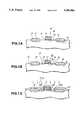
- FIGS. 1A, 1B and 1Care sectional views for showing a MOS fabricating process according to a first embodiment of the present invention.
- FIGS. 2A and 2Bare sectional views for showing a bipolar fabricating process according to a second embodiment of the present invention.
- FIG. 3is a graph showing variation of the temperature of a substrate during rapid thermal annealing.
- FIG. 4is a graph showing variation of the temperature of a substrate during pulsed laser annealing.
- FIG. 5is a sectional view illustrating points defects produced by ion bombardment.
- FIG. 6is a graph showing a reverse leakage current at a junction, annealed only by pulsed laser irradiation.
- FIG. 7is a graph showing a reverse leakage current in the structure obtained by the process according to the first embodiment.
- FIGS. 8is a graph for showing absorption coefficients for different laser pulses which can be employed in the embodiments of the present invention.
- An upper horizontal axisindicates the wavelength (nm), and a lower horizontal axis indicates the photoenergy (or photon energy)(eV).
- FIGS. 1A ⁇ 1Cshow a fabricating process according to a first embodiment in which the invention is applied to a MOS transistor fabricating process.
- a known methodis used to form at least one isolation structure of an isolation layer 12 formed on a silicon substrate 11, and a channel stop ion implant layer 13 formed underneath the isolation layer 12. Then, a gate oxide film 14 is formed, and thereafter a threshold voltage adjusting ion implant layer 15 is formed. Then, the gate oxide layer 14 is covered with a gate polysilicon layer 16, and a silicide layer 17 is formed on the gate polysilicon layer 16. The silicide of the layer 17 is an intermetallic compound of metal and silicon. Then, the silicide layer 17, the gate polysilicon layer 16 and the gate oxide film 14 are patterned to form an insulated gate electrode structure (or region) 18, as shown in FIG. 1A.
- a next stepis for forming LDD (Lightly Doped Drain-source) regions 19 by ion implantation, as shown in FIG. 1B.
- furnace annealing or rapid thermal annealingis performed to activate the various conductive layers and underlying layers formed in the preceding steps, to lower the resistance of the silicide layer 17, and to obtain a Gaussian distribution of the impurity in the LDD regions 19.
- RTArapid thermal annealing
- At least one side wall spacer 20is formed, by a known method, on the side wall of the gate electrode. Then, ion implantation is performed to a source region 21A and a drain region 21B. In this ion implantation step, it is possible to employ the following implantation conditions, for example.
- the implantation energyis 5 ⁇ 20 keV and the dose is 1 ⁇ 10 15 ⁇ 3 ⁇ 10 15 /cm 2 in the case of arsenic ions (As + ).
- the implantation energyis 5 ⁇ 20 keV and the dose is 1 ⁇ 10 15 3 ⁇ 10 15 /cm 2 in the case of BF 2 + ions.
- an oxide film 22is formed to a film thickness of 50 nm, as an anti-reflection film, according to the need, by chemical vapor deposition (CVD).
- CVDchemical vapor deposition
- this low-temperature annealing stepis a 600° C. (electric) furnace anneal.
- the ions implanted into the source region 21A and the drain region 21Bare activated by irradiation of pulsed laser light upon the silicon substrate, as shown in FIG. 1C.
- the conditions of this activating anneal using the pulse laserare as follows:
- the laser usedis a XeCl laser; the irradiation energy is 700 mJ/cm 2 ; and the pulse width is 44 nsec.
- the semiconductor deviceis completed by process steps which are known per se. In these subsequent steps, it is important to limit the temperature of heat treatment of the semiconductor device to 600° C.
- the semiconductor deviceundergoes only heat treatments at temperatures equal to or lower than 600° C.
- the point defects formed by the ion bombardment into the source region 21A and the drain region 21Bare effectively removed at temperatures equal to or lower than the activating anneal temperature, and the implanted impurity particles barely diffuse at annealing temperatures of 600° ⁇ 700° C. Therefore, the low-temperature annealing step can effectively reduce the point defects without deepening the junction.
- the combination of the low-temperature annealing and the pulse laser irradiationcan restrain the reverse leakage current as shown in FIG. 7.
- the activation of the source and drain regions 21A and 21Bis achieved by the pulse laser irradiation, so that the shallow junction structure can be maintained.
- the fabricating process of the inventionmakes it possible to fabricate very high speed integrated circuit devices constituted by miniature transistors.
- FIGS. 2A and 2Bshows a fabricating process according to a second embodiment of the present invention.
- the process of the second embodimentis for a bipolar transistor.
- a buried layer 32is formed between a substrate 31 and an epitaxial layer 33 by known process steps.
- the buried layer 32is formed in the P-type silicon substrate 31 by diffusion of arsenic (As), and then the n-type overlying layer 33 is formed by epitaxial growth.
- the epitaxial layer 33is selectively oxidized to form isolation wall (not shown), and then a base region (or layer) 34 is formed by ion implantation of boron (B).
- the next stepis a known step to form an emitter region (or layer) 35 which is a shallow ion implant layer. Then a low-temperature anneal follows to reduce point defects formed by ion bombardment.
- pulsed laser beamis irradiated onto the top surface of the device to activate the emitter region 35.
- the laseris a XeCl
- the irradiation energyis 700 mJ/cm 2
- the pulse widthis 44 nsec.
- the step of low-temperature annealingcan remove the point defects formed by ion implantation to the emitter region 35, and the step of pulse laser irradiation can activate the emitter region 35 while maintaining the shallow junction.
- the pulse laser irradiationis used to activate the emitter region 35. It is, however, possible to use the pulse laser irradiation for activation of the base region 34.
Landscapes
- Physics & Mathematics (AREA)
- Engineering & Computer Science (AREA)
- High Energy & Nuclear Physics (AREA)
- General Physics & Mathematics (AREA)
- Toxicology (AREA)
- Condensed Matter Physics & Semiconductors (AREA)
- Health & Medical Sciences (AREA)
- Manufacturing & Machinery (AREA)
- Computer Hardware Design (AREA)
- Microelectronics & Electronic Packaging (AREA)
- Power Engineering (AREA)
- Electromagnetism (AREA)
- Optics & Photonics (AREA)
- Insulated Gate Type Field-Effect Transistor (AREA)
Abstract
Description
This is a continuation of application Ser. No. 08/105,154, filed Aug. 12, 1993, now abandoned.
The present invention relates to a process for fabricating semiconductor devices, and more specifically to a semiconductor fabricating process including one or more steps for recovering the crystal damage resulting from ion implantation, and activating carriers.
In semiconductor fabricating processes, various high temperature heat treatments are required to separate or interconnect a plurality of semiconductor devices which are formed in and on a single semiconductor substrate. Usually, ion implantation for forming a LDD (Lightly Doped Drain) structure, or source/drain regions usually results in crystal damage. In order to improve the crystallinity of a semiconductor substrate and to electrically activate implanted acceptor or donor ions, the ion implantation is followed by a step of activation annealing. Furthermore, in order to reduce a contact resistance, a silicide layer of compound consisting of Si and metal, such as refractory metal (W, Mo, Ti, etc.), Pt or Pd, requires a high temperature heating step. Conventional fabricating processes employ, as the activating anneal or high-temperature heat treatment, furnace annealing or rapid thermal annealing (RTA).
With advance in the IC technology, each IC component becomes smaller in size, and a shallower junction is required for source and drain regions, and emitter and base regions. The furnace annealing and rapid thermal annealing make the diffusion deeper, however, and these annealing methods cannot satisfy the demand for device miniaturization and higher packing density. During the activating anneal subsequent to the ion implantation, the diffusion proceeds not only vertically in the direction to deepen the source and drain diffusion regions, but also sideways so as to broaden the lateral dimension. This lateral diffusion tends to increase the possibility of punch-through specifically in a miniaturized MOS transistor having a short gate length. Annealing at a lower temperature can avoid these undesirable diffusion effects and keep shallow implants shallow. In this case, however, the resistivity remains high, the device's current handling characteristic becomes poor, and the transistor is unable to provide required switching performance.
The time required for rapid thermal annealing is not short enough. FIG. 3 shows one example in which the substrate is heated at about 1400° C. The rate of increase of temperature is 100° C./sec, and a rise of temperature takes a considerable time. The duration t during which the substrate is held at the peak temperature is equal to or more than one second, at least. The duration of the peak temperature is still too long to achieve a desired shallow source-drain junction structure in a minute transistor having a gate length (Lg) as short as 0.5˜0.35 μm, for instance. Moreover, infrared radiation used in RTA is absorbed unevenly by SiO2 films on top of the substrate and other topside films having different infrared absorption characteristics.
Pulsed laser irradiation is another method which can be employed for the activating anneal to form a shallow doped region. The laser pulse energy is absorbed by the surface (about 20 nm) of the semiconductor substrate, so that the pulse laser annealing is possible only at a depth of about 100 nm or less, even if thermal diffusion is taken into account. The temperature increase of the wafer as a whole is very small (about 1°˜2° C.). The pulsed laser annealing is, therefore, suitable for activation annealing to form a shallow LDD structure, or source-drain pair.
In the case of the pulse laser activation annealing, however, the time of heat treatment is very short (t=100 nsec, for instance) as shown by a profile of the substrate temperature during irradiation in FIG. 4. Therefore, it is not possible to clear asilicon substrate 1 ofpoint defects 2 formed at levels deeper than the junction of an ion implanted region 1a, such as a source/drain region. The remaining point defects cause an increase of leakage current given an application of reverse voltage. FIG. 6 shows a relationship between reverse voltage and reverse leakage current in a junction accompanied bysuch points defects 2. In the example of FIG. 6, only the pulse laser annealing is applied.
This problem can be solved by increasing the power of the laser to heat deeper regions in the substrate. However, this solution deepens and broadens the implant dopant profile as in the conventional furnace annealing or RTA. Furthermore, high energy laser pulses melt the semiconductor surface to a greater depth and damages the flatness or planarity of the semiconductor substrate surface. Low energy laser pulses melt only a very thin surface layer, and allows a flat surface to be immediately formed again.
It is, therefore, an object of the present invention to provide a semiconductor fabricating process which can form shallower, finer scale, junction structures and reduce junction leakage current.
According to the present invention, a fabricating process comprises an ion-implanting step for forming an ion implant layer (or region) in a semiconductor substrate by ion implantation; a low-temperature annealing step for annealing the semiconductor substrate; and an activating step for activating implanted ions in the ion implant layer by pulse laser irradiation onto the surface of the semiconductor substrate.
The low-temperature annealing step is effective for removing point defects deeper than the implant layer, so that the resulting structure can reduce the current generated by the point defects around the junction, and reduce the leak current. By the pulse laser irradiation, the shallow ion implant layer is activated and the shallow junction is maintained.
Preferably, the low-temperature annealing is performed in the temperature range of 550°˜850° C. in which crystallization of amorphous silicon is possible. A more preferable range of the annealing temperature at the low-temperature annealing step is 600°˜700° C. The annealing time is from 30 minutes to six hours, and more preferably 1˜3 hours. A higher annealing temperature or a longer annealing time would result in a deeper junction.
In the activating step of pulse laser annealing, usable lasers are. A ruby laser (wavelength: 694 nm), XeF (wavelength: 351 nm), XeCl (wavelength: 308 nm), KrF (wavelength: 249 nm), and ArF (wavelength: 193 nm). Preferable lasers are a XeF laser and a XeCl laser. The wavelengths of these lasers are in a range in which the absorption coefficients of Si crystal and boron (B) ion implanted Si crystal become approximately equal to each other as shown in FIG. 8, so that the irradiation energy is absorbed equally. The irradiation energy of the pulse laser anneal ranges from 650 to 1100 mJ/cm2. The preferable range is 700˜900 mJ/cm2. The preferable range of the pulse width is 20˜100 nsec. The irradiation interval can be determined arbitrarily.
Crystalline silicon and amorphous silicon have high absorption coefficients with respect to short wavelength laser pulses. For example, the absorption coefficient is as high as 1.4×106 cm-1 for XeCl (wavelength: 308 nm). The absorption coefficient is a factor (or parameter) representing a light intensity distribution, and is given by the following equation:
I=I.sub.o exp(-αx)
where I is the intensity of light, Io is the intensity of light incident on a surface of substance, α is the absorption coefficient (cm-1), and x is a depth (cm). That is, the light intensity decays, at a depth of 1/α, to 1/e (about one third) of the intensity at the surface. In the case of XeCl, 2/3 of the radiation energy is absorbed up to a depth of 70 Å from the surface, and most is converted to heat. In this way, short wavelength pulsed laser irradiation makes it possible to heat only a very shallow layer in a semiconductor substrate.
FIGS. 1A, 1B and 1C are sectional views for showing a MOS fabricating process according to a first embodiment of the present invention.
FIGS. 2A and 2B are sectional views for showing a bipolar fabricating process according to a second embodiment of the present invention.
FIG. 3 is a graph showing variation of the temperature of a substrate during rapid thermal annealing.
FIG. 4 is a graph showing variation of the temperature of a substrate during pulsed laser annealing.
FIG. 5 is a sectional view illustrating points defects produced by ion bombardment.
FIG. 6 is a graph showing a reverse leakage current at a junction, annealed only by pulsed laser irradiation.
FIG. 7 is a graph showing a reverse leakage current in the structure obtained by the process according to the first embodiment.
FIGS. 8 is a graph for showing absorption coefficients for different laser pulses which can be employed in the embodiments of the present invention. An upper horizontal axis indicates the wavelength (nm), and a lower horizontal axis indicates the photoenergy (or photon energy)(eV).
FIGS. 1A˜1C show a fabricating process according to a first embodiment in which the invention is applied to a MOS transistor fabricating process.
First, a known method is used to form at least one isolation structure of anisolation layer 12 formed on a silicon substrate 11, and a channel stopion implant layer 13 formed underneath theisolation layer 12. Then, agate oxide film 14 is formed, and thereafter a threshold voltage adjustingion implant layer 15 is formed. Then, thegate oxide layer 14 is covered with agate polysilicon layer 16, and asilicide layer 17 is formed on thegate polysilicon layer 16. The silicide of thelayer 17 is an intermetallic compound of metal and silicon. Then, thesilicide layer 17, thegate polysilicon layer 16 and thegate oxide film 14 are patterned to form an insulated gate electrode structure (or region) 18, as shown in FIG. 1A.
A next step is for forming LDD (Lightly Doped Drain-source)regions 19 by ion implantation, as shown in FIG. 1B. Then, furnace annealing or rapid thermal annealing (RTA) is performed to activate the various conductive layers and underlying layers formed in the preceding steps, to lower the resistance of thesilicide layer 17, and to obtain a Gaussian distribution of the impurity in theLDD regions 19. This example employs the rapid thermal annealing for 10 seconds at 1050° C.
Subsequently, at least oneside wall spacer 20 is formed, by a known method, on the side wall of the gate electrode. Then, ion implantation is performed to a source region 21A and a drain region 21B. In this ion implantation step, it is possible to employ the following implantation conditions, for example. The implantation energy is 5˜20 keV and the dose is 1×10¹⁵ ˜3×10¹⁵ /cm2 in the case of arsenic ions (As+). The implantation energy is 5˜20 keV and the dose is 1×10¹⁵ 3×10¹⁵ /cm2 in the case of BF2+ ions.
Then, anoxide film 22 is formed to a film thickness of 50 nm, as an anti-reflection film, according to the need, by chemical vapor deposition (CVD).
Then, a low-temperature annealing is performed at 600° C. In this example, this low-temperature annealing step is a 600° C. (electric) furnace anneal.
After the low-temperature anneal, the ions implanted into the source region 21A and the drain region 21B are activated by irradiation of pulsed laser light upon the silicon substrate, as shown in FIG. 1C. In this example, the conditions of this activating anneal using the pulse laser are as follows: The laser used is a XeCl laser; the irradiation energy is 700 mJ/cm2 ; and the pulse width is 44 nsec.
Subsequently, the semiconductor device is completed by process steps which are known per se. In these subsequent steps, it is important to limit the temperature of heat treatment of the semiconductor device to 600° C. The semiconductor device undergoes only heat treatments at temperatures equal to or lower than 600° C.
In this embodiment, the point defects formed by the ion bombardment into the source region 21A and the drain region 21B are effectively removed at temperatures equal to or lower than the activating anneal temperature, and the implanted impurity particles barely diffuse at annealing temperatures of 600°˜700° C. Therefore, the low-temperature annealing step can effectively reduce the point defects without deepening the junction. The combination of the low-temperature annealing and the pulse laser irradiation can restrain the reverse leakage current as shown in FIG. 7. The activation of the source and drain regions 21A and 21B is achieved by the pulse laser irradiation, so that the shallow junction structure can be maintained. The fabricating process of the invention makes it possible to fabricate very high speed integrated circuit devices constituted by miniature transistors.
FIGS. 2A and 2B shows a fabricating process according to a second embodiment of the present invention. The process of the second embodiment is for a bipolar transistor.
First, a buriedlayer 32 is formed between asubstrate 31 and anepitaxial layer 33 by known process steps. In this example, the buriedlayer 32 is formed in the P-type silicon substrate 31 by diffusion of arsenic (As), and then the n-type overlying layer 33 is formed by epitaxial growth. Thereafter, theepitaxial layer 33 is selectively oxidized to form isolation wall (not shown), and then a base region (or layer) 34 is formed by ion implantation of boron (B).
The next step is a known step to form an emitter region (or layer) 35 which is a shallow ion implant layer. Then a low-temperature anneal follows to reduce point defects formed by ion bombardment.
Next to the low-temperate anneal, pulsed laser beam is irradiated onto the top surface of the device to activate theemitter region 35. In the pulse laser activating annealing step of this example, the laser is a XeCl, the irradiation energy is 700 mJ/cm2, and the pulse width is 44 nsec.
In the second embodiment, the step of low-temperature annealing can remove the point defects formed by ion implantation to theemitter region 35, and the step of pulse laser irradiation can activate theemitter region 35 while maintaining the shallow junction. In this embodiment, the pulse laser irradiation is used to activate theemitter region 35. It is, however, possible to use the pulse laser irradiation for activation of thebase region 34.
Although various minor changes and modifications might be suggested by those skilled in this art, it will be apparent that I wish to include within the claims of the patent warranted hereon all such changes and modifications as reasonably come within my contribution to the art.
Claims (15)
1. A semiconductor device fabricating process, comprising the steps of:
ion-implanting impurity ions into a semiconductor substrate to form a shallow ion implant layer in a surface region of the semiconductor substrate;
annealing the semiconductor substrate by heating the semiconductor substrate which has the shallow ion implant layer to a temperature of 550° C. to 850° C. to reduce point defects but without deepening the shallow ion implant layer;
radiating a pulsed laser on the semiconductor substrate to activate the implanted ions of the shallow ion implant layer while maintaining the depth of the shallow ion implant layer; and performing said radiating step by a laser beam having an energy density in a range of 650 to 1100 mJ/cm2.
2. A semiconductor device fabricating process according to claim 1 wherein said ion implantation comprises forming an active region of a transistor.
3. A semiconductor device fabricating process according to claim 2 wherein said ion implantation includes forming source and drain regions of a field effect transistor.
4. A semiconductor device fabricating process according to claim 3 further comprising a doping step for forming a lightly doped region by ion implantation in the semiconductor substrate before the ion implanting step; and an annealing step for annealing the semiconductor substrate by one of furnace annealing and rapid thermal annealing to form a Gaussian distribution of impurity ions in the lightly doped region.
5. A semiconductor device fabricating process according to claim 4 wherein said process further comprises forming an anti-reflection film between said ion implantation of said implant layer and said low temperature annealing.
6. A semiconductor device fabricating process according to claim 5 wherein said anti-reflection film is an oxide film formed by chemical vapor deposition.
7. A semiconductor device fabricating process according to claim 4 wherein said process further comprises forming a polysilicon gate structure before said doping ion implantation.
8. A semiconductor device fabricating process according to claim 2 wherein said ion implantation includes forming one of an emitter region and a base region of a bipolar transistor.
9. A semiconductor device fabricating process according to claim 8 wherein said process further comprises a base doping for forming said base region extending into said substrate from said surface of said substrate, and said ion implantation includes forming said emitter region in said base region, said emitter region formed by said ion implantation being shallower from said surface of said substrate than said base region.
10. A semiconductor device fabricating process according to claim 9 wherein said process further comprises forming said substrate which is an epitaxial substrate comprising an original substrate layer, an epitaxial layer grown on said original substrate layer and a buried layer formed between said original substrate layer and said epitaxial layer, said base and emitter regions being formed in said epitaxial layer.
11. A semiconductor device fabricating process according to claim 1 wherein said activating of the implanted ions is achieved by irradiation of the pulsed laser radiation of a wavelength at which a photon absorption coefficient of said semiconductor substrate is greater than 1×106 cm-1, with irradiation energy in a range from 650 to 1100 mJ/cm2.
12. A semiconductor device fabricating process according to claim 11 wherein the irradiation of the pulsed laser radiation of said activating of the implanted ions is performed by using one of a ruby laser, a XeF laser, a XeCl laser, a KrF laser and an ArF laser.
13. A semiconductor device fabricating process according to claim 1 wherein said annealing temperature is in a range of 600° C. to 700° C.
14. A semiconductor device fabricating process as claimed in claim 1 wherein a pulse width of the laser beam is in a range of 20 to 100 nsec.
15. A semiconductor device fabricating process according to claim 1 wherein said annealing is carried out for a duration of 30 minutes to 6 hours.
Priority Applications (1)
| Application Number | Priority Date | Filing Date | Title |
|---|---|---|---|
| US08/248,596US5399506A (en) | 1992-08-13 | 1994-05-24 | Semiconductor fabricating process |
Applications Claiming Priority (4)
| Application Number | Priority Date | Filing Date | Title |
|---|---|---|---|
| JP4-215325 | 1992-08-13 | ||
| JP21532592AJP3211394B2 (en) | 1992-08-13 | 1992-08-13 | Method for manufacturing semiconductor device |
| US10515493A | 1993-08-12 | 1993-08-12 | |
| US08/248,596US5399506A (en) | 1992-08-13 | 1994-05-24 | Semiconductor fabricating process |
Related Parent Applications (1)
| Application Number | Title | Priority Date | Filing Date |
|---|---|---|---|
| US10515493AContinuation | 1992-08-13 | 1993-08-12 |
Publications (1)
| Publication Number | Publication Date |
|---|---|
| US5399506Atrue US5399506A (en) | 1995-03-21 |
Family
ID=16670435
Family Applications (1)
| Application Number | Title | Priority Date | Filing Date |
|---|---|---|---|
| US08/248,596Expired - Fee RelatedUS5399506A (en) | 1992-08-13 | 1994-05-24 | Semiconductor fabricating process |
Country Status (2)
| Country | Link |
|---|---|
| US (1) | US5399506A (en) |
| JP (1) | JP3211394B2 (en) |
Cited By (76)
| Publication number | Priority date | Publication date | Assignee | Title |
|---|---|---|---|---|
| US5474940A (en)* | 1992-01-08 | 1995-12-12 | Sony Corporation | Method of fabricating a semiconductor device having shallow junctions in source-drain regions and a gate electrode with a low resistance silicide layer |
| US5683920A (en)* | 1995-12-29 | 1997-11-04 | Hyundai Electronics Industries Co., Ltd. | Method for fabricating semiconductor devices |
| US5773337A (en)* | 1996-12-31 | 1998-06-30 | Hyundai Electronics Industries Co., Ltd. | Method for forming ultra-shallow junction of semiconductor device |
| US5966605A (en)* | 1997-11-07 | 1999-10-12 | Advanced Micro Devices, Inc. | Reduction of poly depletion in semiconductor integrated circuits |
| US6040224A (en)* | 1993-08-30 | 2000-03-21 | Sony Corporation | Method of manufacturing semiconductor devices |
| US6057185A (en)* | 1995-09-08 | 2000-05-02 | Sony Corporation | Method of manufacturing semiconductor device |
| US6131257A (en)* | 1993-11-25 | 2000-10-17 | Fujitsu Limited | Method of making a surface acoustic wave device |
| US6136672A (en)* | 1998-04-17 | 2000-10-24 | Lucent Technologies Inc. | Process for device fabrication using a high-energy boron implant |
| US6197646B1 (en) | 1993-02-12 | 2001-03-06 | Fujitsu Limited | Manufacture of semiconductor device with salicide electrode |
| US6287925B1 (en)* | 2000-02-24 | 2001-09-11 | Advanced Micro Devices, Inc. | Formation of highly conductive junctions by rapid thermal anneal and laser thermal process |
| WO2001071787A1 (en)* | 2000-03-17 | 2001-09-27 | Varian Semiconductor Equipment Associates, Inc. | Method of forming ultrashallow junctions by laser annealing and rapid thermal annealing |
| US6297135B1 (en) | 1997-01-29 | 2001-10-02 | Ultratech Stepper, Inc. | Method for forming silicide regions on an integrated device |
| US6365476B1 (en)* | 2000-10-27 | 2002-04-02 | Ultratech Stepper, Inc. | Laser thermal process for fabricating field-effect transistors |
| US6387803B2 (en) | 1997-01-29 | 2002-05-14 | Ultratech Stepper, Inc. | Method for forming a silicide region on a silicon body |
| US6444549B2 (en)* | 1997-09-12 | 2002-09-03 | Nec Corporation | Thermal processing of semiconductor devices |
| US6451704B1 (en) | 2001-05-07 | 2002-09-17 | Chartered Semiconductor Manufacturing Ltd. | Method for forming PLDD structure with minimized lateral dopant diffusion |
| US6559015B1 (en)* | 2001-06-01 | 2003-05-06 | Advanced Micro Devices, Inc. | Fabrication of field effect transistor with dual laser thermal anneal processes |
| US6594446B2 (en) | 2000-12-04 | 2003-07-15 | Vortek Industries Ltd. | Heat-treating methods and systems |
| US20040106243A1 (en)* | 2002-11-20 | 2004-06-03 | Takeshi Karasawa | Method for controlling electrical conductivity |
| US20040115871A1 (en)* | 2002-10-02 | 2004-06-17 | Tomokazu Kawamoto | Method for fabricating semiconductor device |
| US6797602B1 (en)* | 2001-02-09 | 2004-09-28 | Advanced Micro Devices, Inc. | Method of manufacturing a semiconductor device with supersaturated source/drain extensions and metal silicide contacts |
| US20040235281A1 (en)* | 2003-04-25 | 2004-11-25 | Downey Daniel F. | Apparatus and methods for junction formation using optical illumination |
| US6825101B1 (en)* | 2000-03-27 | 2004-11-30 | Ultratech, Inc. | Methods for annealing a substrate and article produced by such methods |
| US20050020095A1 (en)* | 2001-08-23 | 2005-01-27 | Johannes Baur | Method for surface treating a semiconductor |
| US20050023577A1 (en)* | 2003-06-17 | 2005-02-03 | Takayuki Ito | Semiconductor device including a semiconductor substrate formed with a shallow impurity region, and a fabrication method for the same |
| US20050063453A1 (en)* | 2001-12-26 | 2005-03-24 | Camm David Malcolm | Temperature measurement and heat-treating metods and system |
| US20050133167A1 (en)* | 2003-12-19 | 2005-06-23 | Camm David M. | Apparatuses and methods for suppressing thermally-induced motion of a workpiece |
| US20050158956A1 (en)* | 2004-01-16 | 2005-07-21 | Chartered Semiconductor Manufacturing Ltd. | Dual step source/drain extension junction anneal to reduce the junction depth: multiple-pulse low energy laser anneal coupled with rapid thermal anneal |
| US20050186765A1 (en)* | 2004-02-23 | 2005-08-25 | Yi Ma | Gate electrode dopant activation method for semiconductor manufacturing |
| US7091093B1 (en)* | 1999-09-17 | 2006-08-15 | Matsushita Electric Industrial Co., Ltd. | Method for fabricating a semiconductor device having a pocket dopant diffused layer |
| US20070066023A1 (en)* | 2005-09-20 | 2007-03-22 | Randhir Thakur | Method to form a device on a soi substrate |
| US20080157452A1 (en)* | 2006-11-15 | 2008-07-03 | Mattson Technology Canada, Inc. | Systems and methods for supporting a workpiece during heat-treating |
| US20090047768A1 (en)* | 2007-08-15 | 2009-02-19 | Texas Instruments Incorporated | Formation of shallow junctions by diffusion from a dielectric doped by cluster or molecular ion beams |
| US20090101894A1 (en)* | 2006-02-22 | 2009-04-23 | Hsiao Tsai-Fu | Method for fabricating metal-oxide semiconductor transistors |
| US20110033998A1 (en)* | 2009-08-07 | 2011-02-10 | Varian Semiconductor Equipment Associates, Inc. | Optimized halo or pocket cold implants |
| US20110034013A1 (en)* | 2009-08-07 | 2011-02-10 | Varian Semiconductor Equipment Associates, Inc. | Low Temperature Ion Implantation |
| US20110076823A1 (en)* | 2009-09-28 | 2011-03-31 | Huang-Yi Lin | Method for fabricating a semiconductor device |
| US8324059B2 (en) | 2011-04-25 | 2012-12-04 | United Microelectronics Corp. | Method of fabricating a semiconductor structure |
| US8426284B2 (en) | 2011-05-11 | 2013-04-23 | United Microelectronics Corp. | Manufacturing method for semiconductor structure |
| US8431460B2 (en) | 2011-05-27 | 2013-04-30 | United Microelectronics Corp. | Method for fabricating semiconductor device |
| US8434341B2 (en) | 2002-12-20 | 2013-05-07 | Mattson Technology, Inc. | Methods and systems for supporting a workpiece and for heat-treating the workpiece |
| US8445363B2 (en) | 2011-04-21 | 2013-05-21 | United Microelectronics Corp. | Method of fabricating an epitaxial layer |
| US8466502B2 (en) | 2011-03-24 | 2013-06-18 | United Microelectronics Corp. | Metal-gate CMOS device |
| US8476169B2 (en) | 2011-10-17 | 2013-07-02 | United Microelectronics Corp. | Method of making strained silicon channel semiconductor structure |
| US8481391B2 (en) | 2011-05-18 | 2013-07-09 | United Microelectronics Corp. | Process for manufacturing stress-providing structure and semiconductor device with such stress-providing structure |
| US8564063B2 (en) | 2010-12-07 | 2013-10-22 | United Microelectronics Corp. | Semiconductor device having metal gate and manufacturing method thereof |
| US8575043B2 (en) | 2011-07-26 | 2013-11-05 | United Microelectronics Corp. | Semiconductor device and manufacturing method thereof |
| US8647953B2 (en) | 2011-11-17 | 2014-02-11 | United Microelectronics Corp. | Method for fabricating first and second epitaxial cap layers |
| US8647941B2 (en) | 2011-08-17 | 2014-02-11 | United Microelectronics Corp. | Method of forming semiconductor device |
| US8664069B2 (en) | 2012-04-05 | 2014-03-04 | United Microelectronics Corp. | Semiconductor structure and process thereof |
| US8674433B2 (en) | 2011-08-24 | 2014-03-18 | United Microelectronics Corp. | Semiconductor process |
| US8691659B2 (en) | 2011-10-26 | 2014-04-08 | United Microelectronics Corp. | Method for forming void-free dielectric layer |
| US8710632B2 (en) | 2012-09-07 | 2014-04-29 | United Microelectronics Corp. | Compound semiconductor epitaxial structure and method for fabricating the same |
| US8709930B2 (en) | 2011-11-25 | 2014-04-29 | United Microelectronics Corp. | Semiconductor process |
| US8716750B2 (en) | 2011-07-25 | 2014-05-06 | United Microelectronics Corp. | Semiconductor device having epitaxial structures |
| US8754448B2 (en) | 2011-11-01 | 2014-06-17 | United Microelectronics Corp. | Semiconductor device having epitaxial layer |
| US8753902B1 (en) | 2013-03-13 | 2014-06-17 | United Microelectronics Corp. | Method of controlling etching process for forming epitaxial structure |
| US8765546B1 (en) | 2013-06-24 | 2014-07-01 | United Microelectronics Corp. | Method for fabricating fin-shaped field-effect transistor |
| US8796695B2 (en) | 2012-06-22 | 2014-08-05 | United Microelectronics Corp. | Multi-gate field-effect transistor and process thereof |
| US8835243B2 (en) | 2012-05-04 | 2014-09-16 | United Microelectronics Corp. | Semiconductor process |
| US8853060B1 (en) | 2013-05-27 | 2014-10-07 | United Microelectronics Corp. | Epitaxial process |
| US8866230B2 (en) | 2012-04-26 | 2014-10-21 | United Microelectronics Corp. | Semiconductor devices |
| US8895396B1 (en) | 2013-07-11 | 2014-11-25 | United Microelectronics Corp. | Epitaxial Process of forming stress inducing epitaxial layers in source and drain regions of PMOS and NMOS structures |
| US8951876B2 (en) | 2012-06-20 | 2015-02-10 | United Microelectronics Corp. | Semiconductor device and manufacturing method thereof |
| US8981487B2 (en) | 2013-07-31 | 2015-03-17 | United Microelectronics Corp. | Fin-shaped field-effect transistor (FinFET) |
| US9034705B2 (en) | 2013-03-26 | 2015-05-19 | United Microelectronics Corp. | Method of forming semiconductor device |
| US9064893B2 (en) | 2013-05-13 | 2015-06-23 | United Microelectronics Corp. | Gradient dopant of strained substrate manufacturing method of semiconductor device |
| US9070590B2 (en) | 2008-05-16 | 2015-06-30 | Mattson Technology, Inc. | Workpiece breakage prevention method and apparatus |
| US9076652B2 (en) | 2013-05-27 | 2015-07-07 | United Microelectronics Corp. | Semiconductor process for modifying shape of recess |
| US9117925B2 (en) | 2013-01-31 | 2015-08-25 | United Microelectronics Corp. | Epitaxial process |
| US9136348B2 (en) | 2012-03-12 | 2015-09-15 | United Microelectronics Corp. | Semiconductor structure and fabrication method thereof |
| US9202914B2 (en) | 2012-03-14 | 2015-12-01 | United Microelectronics Corporation | Semiconductor device and method for fabricating the same |
| RU2602402C1 (en)* | 2015-08-14 | 2016-11-20 | Федеральное государственное унитарное предприятие "Всероссийский научно-исследовательский институт автоматики им. Н.Л. Духова" (ФГУП "ВНИИА") | Method of laser processing of nonmetallic plates |
| US20180138287A1 (en)* | 2016-11-15 | 2018-05-17 | Fuji Electric Co., Ltd. | Method of manufacturing silicon carbide semiconductor device |
| CN109065441A (en)* | 2013-06-26 | 2018-12-21 | 富士电机株式会社 | The manufacturing method of semiconductor device and semiconductor device |
| US10236348B2 (en) | 2016-11-15 | 2019-03-19 | Fuji Electric Co., Ltd. | Silicon carbide semiconductor device with double trench and method of making same |
Families Citing this family (6)
| Publication number | Priority date | Publication date | Assignee | Title |
|---|---|---|---|---|
| KR100522758B1 (en)* | 2000-06-28 | 2005-10-21 | 주식회사 하이닉스반도체 | Method for manufacturing semiconductor device |
| JP4967205B2 (en)* | 2001-08-09 | 2012-07-04 | 富士電機株式会社 | Manufacturing method of semiconductor device |
| JP4639040B2 (en)* | 2002-10-10 | 2011-02-23 | パナソニック株式会社 | Manufacturing method of semiconductor device |
| JP4733912B2 (en) | 2003-04-03 | 2011-07-27 | 株式会社東芝 | Manufacturing method of semiconductor device |
| JP2004356322A (en)* | 2003-05-28 | 2004-12-16 | Matsushita Electric Ind Co Ltd | Semiconductor device manufacturing method and semiconductor manufacturing apparatus |
| JP5246716B2 (en)* | 2009-11-25 | 2013-07-24 | 株式会社日本製鋼所 | Semiconductor substrate manufacturing method and laser annealing apparatus |
Citations (5)
| Publication number | Priority date | Publication date | Assignee | Title |
|---|---|---|---|---|
| US4151008A (en)* | 1974-11-15 | 1979-04-24 | Spire Corporation | Method involving pulsed light processing of semiconductor devices |
| US4331485A (en)* | 1980-03-03 | 1982-05-25 | Arnon Gat | Method for heat treating semiconductor material using high intensity CW lamps |
| US4379727A (en)* | 1981-07-08 | 1983-04-12 | International Business Machines Corporation | Method of laser annealing of subsurface ion implanted regions |
| US4646426A (en)* | 1981-02-16 | 1987-03-03 | Fujitsu Limited | Method of producing MOS FET type semiconductor device |
| JPH01187814A (en)* | 1988-01-22 | 1989-07-27 | Hitachi Ltd | Manufacture of thin film semiconductor device |
- 1992
- 1992-08-13JPJP21532592Apatent/JP3211394B2/ennot_activeExpired - Fee Related
- 1994
- 1994-05-24USUS08/248,596patent/US5399506A/ennot_activeExpired - Fee Related
Patent Citations (5)
| Publication number | Priority date | Publication date | Assignee | Title |
|---|---|---|---|---|
| US4151008A (en)* | 1974-11-15 | 1979-04-24 | Spire Corporation | Method involving pulsed light processing of semiconductor devices |
| US4331485A (en)* | 1980-03-03 | 1982-05-25 | Arnon Gat | Method for heat treating semiconductor material using high intensity CW lamps |
| US4646426A (en)* | 1981-02-16 | 1987-03-03 | Fujitsu Limited | Method of producing MOS FET type semiconductor device |
| US4379727A (en)* | 1981-07-08 | 1983-04-12 | International Business Machines Corporation | Method of laser annealing of subsurface ion implanted regions |
| JPH01187814A (en)* | 1988-01-22 | 1989-07-27 | Hitachi Ltd | Manufacture of thin film semiconductor device |
Non-Patent Citations (2)
| Title |
|---|
| Kwor et al., "Effect of Furnace Preanneal and Rapid Thermal Annealing on Arsenic Implanted Silicon", J. Electr. Soc.; Solid-State Science and Technology, May 1985, pp. 1201-1206. |
| Kwor et al., Effect of Furnace Preanneal and Rapid Thermal Annealing on Arsenic Implanted Silicon , J. Electr. Soc.; Solid State Science and Technology, May 1985, pp. 1201 1206.* |
Cited By (120)
| Publication number | Priority date | Publication date | Assignee | Title |
|---|---|---|---|---|
| US5474940A (en)* | 1992-01-08 | 1995-12-12 | Sony Corporation | Method of fabricating a semiconductor device having shallow junctions in source-drain regions and a gate electrode with a low resistance silicide layer |
| US6197646B1 (en) | 1993-02-12 | 2001-03-06 | Fujitsu Limited | Manufacture of semiconductor device with salicide electrode |
| US6040224A (en)* | 1993-08-30 | 2000-03-21 | Sony Corporation | Method of manufacturing semiconductor devices |
| US6131257A (en)* | 1993-11-25 | 2000-10-17 | Fujitsu Limited | Method of making a surface acoustic wave device |
| US6057185A (en)* | 1995-09-08 | 2000-05-02 | Sony Corporation | Method of manufacturing semiconductor device |
| US5683920A (en)* | 1995-12-29 | 1997-11-04 | Hyundai Electronics Industries Co., Ltd. | Method for fabricating semiconductor devices |
| US5773337A (en)* | 1996-12-31 | 1998-06-30 | Hyundai Electronics Industries Co., Ltd. | Method for forming ultra-shallow junction of semiconductor device |
| US6297135B1 (en) | 1997-01-29 | 2001-10-02 | Ultratech Stepper, Inc. | Method for forming silicide regions on an integrated device |
| US6387803B2 (en) | 1997-01-29 | 2002-05-14 | Ultratech Stepper, Inc. | Method for forming a silicide region on a silicon body |
| US6444549B2 (en)* | 1997-09-12 | 2002-09-03 | Nec Corporation | Thermal processing of semiconductor devices |
| US5966605A (en)* | 1997-11-07 | 1999-10-12 | Advanced Micro Devices, Inc. | Reduction of poly depletion in semiconductor integrated circuits |
| US6136672A (en)* | 1998-04-17 | 2000-10-24 | Lucent Technologies Inc. | Process for device fabrication using a high-energy boron implant |
| US7091093B1 (en)* | 1999-09-17 | 2006-08-15 | Matsushita Electric Industrial Co., Ltd. | Method for fabricating a semiconductor device having a pocket dopant diffused layer |
| US20060202287A1 (en)* | 1999-09-17 | 2006-09-14 | Matsushita Electric Industrial Co., Ltd. | Semiconductor device and method for fabricating the same |
| US6287925B1 (en)* | 2000-02-24 | 2001-09-11 | Advanced Micro Devices, Inc. | Formation of highly conductive junctions by rapid thermal anneal and laser thermal process |
| WO2001071787A1 (en)* | 2000-03-17 | 2001-09-27 | Varian Semiconductor Equipment Associates, Inc. | Method of forming ultrashallow junctions by laser annealing and rapid thermal annealing |
| KR100839259B1 (en)* | 2000-03-17 | 2008-06-17 | 베리안 세미콘덕터 이큅먼트 어소시에이츠, 인크. | Ultra shallow junction formation method by laser annealing and rapid thermal annealing |
| US6825101B1 (en)* | 2000-03-27 | 2004-11-30 | Ultratech, Inc. | Methods for annealing a substrate and article produced by such methods |
| US6365476B1 (en)* | 2000-10-27 | 2002-04-02 | Ultratech Stepper, Inc. | Laser thermal process for fabricating field-effect transistors |
| WO2002035601A1 (en)* | 2000-10-27 | 2002-05-02 | Ultratech Stepper, Inc. | Laser thermal process for fabricating field-effect transistors |
| US6941063B2 (en) | 2000-12-04 | 2005-09-06 | Mattson Technology Canada, Inc. | Heat-treating methods and systems |
| US20030206732A1 (en)* | 2000-12-04 | 2003-11-06 | Camm David Malcolm | Heat-treating methods and systems |
| US6594446B2 (en) | 2000-12-04 | 2003-07-15 | Vortek Industries Ltd. | Heat-treating methods and systems |
| US6963692B2 (en) | 2000-12-04 | 2005-11-08 | Vortek Industries Ltd. | Heat-treating methods and systems |
| US20050062388A1 (en)* | 2000-12-04 | 2005-03-24 | Camm David Malcolm | Heat-treating methods and systems |
| US6797602B1 (en)* | 2001-02-09 | 2004-09-28 | Advanced Micro Devices, Inc. | Method of manufacturing a semiconductor device with supersaturated source/drain extensions and metal silicide contacts |
| US6451704B1 (en) | 2001-05-07 | 2002-09-17 | Chartered Semiconductor Manufacturing Ltd. | Method for forming PLDD structure with minimized lateral dopant diffusion |
| US6559015B1 (en)* | 2001-06-01 | 2003-05-06 | Advanced Micro Devices, Inc. | Fabrication of field effect transistor with dual laser thermal anneal processes |
| US20050020095A1 (en)* | 2001-08-23 | 2005-01-27 | Johannes Baur | Method for surface treating a semiconductor |
| US7445382B2 (en) | 2001-12-26 | 2008-11-04 | Mattson Technology Canada, Inc. | Temperature measurement and heat-treating methods and system |
| US20060096677A1 (en)* | 2001-12-26 | 2006-05-11 | Camm David M | Temperature measurement and heat-treating methods |
| US7616872B2 (en) | 2001-12-26 | 2009-11-10 | Mattson Technology Canada, Inc. | Temperature measurement and heat-treating methods and systems |
| US20050063453A1 (en)* | 2001-12-26 | 2005-03-24 | Camm David Malcolm | Temperature measurement and heat-treating metods and system |
| US6835625B2 (en)* | 2002-10-02 | 2004-12-28 | Fujitsu Limited | Method for fabricating semiconductor device |
| US20040115871A1 (en)* | 2002-10-02 | 2004-06-17 | Tomokazu Kawamoto | Method for fabricating semiconductor device |
| US20040106243A1 (en)* | 2002-11-20 | 2004-06-03 | Takeshi Karasawa | Method for controlling electrical conductivity |
| US6890870B2 (en) | 2002-11-20 | 2005-05-10 | Ushio Denki Kabushiki Kaisha | Method for controlling electrical conductivity |
| US9627244B2 (en) | 2002-12-20 | 2017-04-18 | Mattson Technology, Inc. | Methods and systems for supporting a workpiece and for heat-treating the workpiece |
| US8434341B2 (en) | 2002-12-20 | 2013-05-07 | Mattson Technology, Inc. | Methods and systems for supporting a workpiece and for heat-treating the workpiece |
| US20040235281A1 (en)* | 2003-04-25 | 2004-11-25 | Downey Daniel F. | Apparatus and methods for junction formation using optical illumination |
| US20050023577A1 (en)* | 2003-06-17 | 2005-02-03 | Takayuki Ito | Semiconductor device including a semiconductor substrate formed with a shallow impurity region, and a fabrication method for the same |
| US7189624B2 (en)* | 2003-06-17 | 2007-03-13 | Kabushiki Kaisha Toshiba | Fabrication method for a semiconductor device including a semiconductor substrate formed with a shallow impurity region |
| US7453090B2 (en) | 2003-06-17 | 2008-11-18 | Kabushiki Kaisha Toshiba | Semiconductor device including a semiconductor substrate formed with a shallow impurity region |
| US20070138567A1 (en)* | 2003-06-17 | 2007-06-21 | Kabushiki Kaisha Toshiba | Semiconductor device including a semiconductor substrate formed with a shallow impurity region, and a fabrication method for the same |
| US20050133167A1 (en)* | 2003-12-19 | 2005-06-23 | Camm David M. | Apparatuses and methods for suppressing thermally-induced motion of a workpiece |
| US7501607B2 (en) | 2003-12-19 | 2009-03-10 | Mattson Technology Canada, Inc. | Apparatuses and methods for suppressing thermally-induced motion of a workpiece |
| US7112499B2 (en) | 2004-01-16 | 2006-09-26 | Chartered Semiconductor Manufacturing Ltd. | Dual step source/drain extension junction anneal to reduce the junction depth: multiple-pulse low energy laser anneal coupled with rapid thermal anneal |
| US20050158956A1 (en)* | 2004-01-16 | 2005-07-21 | Chartered Semiconductor Manufacturing Ltd. | Dual step source/drain extension junction anneal to reduce the junction depth: multiple-pulse low energy laser anneal coupled with rapid thermal anneal |
| US7078302B2 (en) | 2004-02-23 | 2006-07-18 | Applied Materials, Inc. | Gate electrode dopant activation method for semiconductor manufacturing including a laser anneal |
| US20050186765A1 (en)* | 2004-02-23 | 2005-08-25 | Yi Ma | Gate electrode dopant activation method for semiconductor manufacturing |
| WO2005083762A1 (en)* | 2004-02-23 | 2005-09-09 | Applied Materials, Inc. | Gate electrode dopant activation method for semiconductor manufacturing |
| US7611976B2 (en) | 2004-02-23 | 2009-11-03 | Applied Materials, Inc. | Gate electrode dopant activation method for semiconductor manufacturing |
| US20060286763A1 (en)* | 2004-02-23 | 2006-12-21 | Yi Ma | Gate electrode dopant activation method for semiconductor manufacturing |
| CN100524630C (en)* | 2004-02-23 | 2009-08-05 | 应用材料股份有限公司 | gate dopant activation method for semiconductor manufacturing |
| WO2005106939A1 (en)* | 2004-04-26 | 2005-11-10 | Varian Semiconductor Equipment Associates, Inc. | Apparatus and methods for junction formation using optical illumination |
| US20070066023A1 (en)* | 2005-09-20 | 2007-03-22 | Randhir Thakur | Method to form a device on a soi substrate |
| US20090101894A1 (en)* | 2006-02-22 | 2009-04-23 | Hsiao Tsai-Fu | Method for fabricating metal-oxide semiconductor transistors |
| US20110159658A1 (en)* | 2006-02-22 | 2011-06-30 | Hsiao Tsai-Fu | Method for fabricating metal-oxide semiconductor transistors |
| US8053847B2 (en) | 2006-02-22 | 2011-11-08 | United Microelectronics Corp. | Method for fabricating metal-oxide semiconductor transistors |
| US8076210B2 (en) | 2006-02-22 | 2011-12-13 | United Microelectronics Corp. | Method for fabricating metal-oxide semiconductor transistors |
| US20080157452A1 (en)* | 2006-11-15 | 2008-07-03 | Mattson Technology Canada, Inc. | Systems and methods for supporting a workpiece during heat-treating |
| US8454356B2 (en) | 2006-11-15 | 2013-06-04 | Mattson Technology, Inc. | Systems and methods for supporting a workpiece during heat-treating |
| US20090047768A1 (en)* | 2007-08-15 | 2009-02-19 | Texas Instruments Incorporated | Formation of shallow junctions by diffusion from a dielectric doped by cluster or molecular ion beams |
| US8580663B2 (en) | 2007-08-15 | 2013-11-12 | Texas Instruments Incorporated | Formation of shallow junctions by diffusion from a dielectronic doped by cluster or molecular ion beams |
| US8026135B2 (en)* | 2007-08-15 | 2011-09-27 | Texas Instruments Incorporated | Formation of shallow junctions by diffusion from a dielectric doped by cluster or molecular ion beams |
| US9070590B2 (en) | 2008-05-16 | 2015-06-30 | Mattson Technology, Inc. | Workpiece breakage prevention method and apparatus |
| US8012843B2 (en)* | 2009-08-07 | 2011-09-06 | Varian Semiconductor Equipment Associates, Inc. | Optimized halo or pocket cold implants |
| US20110033998A1 (en)* | 2009-08-07 | 2011-02-10 | Varian Semiconductor Equipment Associates, Inc. | Optimized halo or pocket cold implants |
| US8101528B2 (en)* | 2009-08-07 | 2012-01-24 | Varian Semiconductor Equipment Associates, Inc. | Low temperature ion implantation |
| US20110034013A1 (en)* | 2009-08-07 | 2011-02-10 | Varian Semiconductor Equipment Associates, Inc. | Low Temperature Ion Implantation |
| US8207043B2 (en) | 2009-09-28 | 2012-06-26 | United Microelectronics Corp. | Method for fabricating a semiconductor device |
| US20110076823A1 (en)* | 2009-09-28 | 2011-03-31 | Huang-Yi Lin | Method for fabricating a semiconductor device |
| US8564063B2 (en) | 2010-12-07 | 2013-10-22 | United Microelectronics Corp. | Semiconductor device having metal gate and manufacturing method thereof |
| US8765591B2 (en) | 2010-12-07 | 2014-07-01 | United Microelectronics Corp. | Semiconductor device having metal gate and manufacturing method thereof |
| US8592271B2 (en) | 2011-03-24 | 2013-11-26 | United Microelectronics Corp. | Metal-gate CMOS device and fabrication method thereof |
| US8466502B2 (en) | 2011-03-24 | 2013-06-18 | United Microelectronics Corp. | Metal-gate CMOS device |
| US8445363B2 (en) | 2011-04-21 | 2013-05-21 | United Microelectronics Corp. | Method of fabricating an epitaxial layer |
| US8324059B2 (en) | 2011-04-25 | 2012-12-04 | United Microelectronics Corp. | Method of fabricating a semiconductor structure |
| US8426284B2 (en) | 2011-05-11 | 2013-04-23 | United Microelectronics Corp. | Manufacturing method for semiconductor structure |
| US8481391B2 (en) | 2011-05-18 | 2013-07-09 | United Microelectronics Corp. | Process for manufacturing stress-providing structure and semiconductor device with such stress-providing structure |
| US8431460B2 (en) | 2011-05-27 | 2013-04-30 | United Microelectronics Corp. | Method for fabricating semiconductor device |
| US8716750B2 (en) | 2011-07-25 | 2014-05-06 | United Microelectronics Corp. | Semiconductor device having epitaxial structures |
| US8575043B2 (en) | 2011-07-26 | 2013-11-05 | United Microelectronics Corp. | Semiconductor device and manufacturing method thereof |
| US8647941B2 (en) | 2011-08-17 | 2014-02-11 | United Microelectronics Corp. | Method of forming semiconductor device |
| US8674433B2 (en) | 2011-08-24 | 2014-03-18 | United Microelectronics Corp. | Semiconductor process |
| US8476169B2 (en) | 2011-10-17 | 2013-07-02 | United Microelectronics Corp. | Method of making strained silicon channel semiconductor structure |
| US8853740B2 (en) | 2011-10-17 | 2014-10-07 | United Microelectronics Corp. | Strained silicon channel semiconductor structure |
| US8691659B2 (en) | 2011-10-26 | 2014-04-08 | United Microelectronics Corp. | Method for forming void-free dielectric layer |
| US8754448B2 (en) | 2011-11-01 | 2014-06-17 | United Microelectronics Corp. | Semiconductor device having epitaxial layer |
| US8927376B2 (en) | 2011-11-01 | 2015-01-06 | United Microelectronics Corp. | Semiconductor device and method of forming epitaxial layer |
| US8647953B2 (en) | 2011-11-17 | 2014-02-11 | United Microelectronics Corp. | Method for fabricating first and second epitaxial cap layers |
| US8709930B2 (en) | 2011-11-25 | 2014-04-29 | United Microelectronics Corp. | Semiconductor process |
| US9312359B2 (en) | 2012-03-12 | 2016-04-12 | United Microelectronics Corp. | Semiconductor structure and fabrication method thereof |
| US9136348B2 (en) | 2012-03-12 | 2015-09-15 | United Microelectronics Corp. | Semiconductor structure and fabrication method thereof |
| US9443970B2 (en) | 2012-03-14 | 2016-09-13 | United Microelectronics Corporation | Semiconductor device with epitaxial structures and method for fabricating the same |
| US9202914B2 (en) | 2012-03-14 | 2015-12-01 | United Microelectronics Corporation | Semiconductor device and method for fabricating the same |
| US8664069B2 (en) | 2012-04-05 | 2014-03-04 | United Microelectronics Corp. | Semiconductor structure and process thereof |
| US8884346B2 (en) | 2012-04-05 | 2014-11-11 | United Microelectronics Corp. | Semiconductor structure |
| US8866230B2 (en) | 2012-04-26 | 2014-10-21 | United Microelectronics Corp. | Semiconductor devices |
| US8835243B2 (en) | 2012-05-04 | 2014-09-16 | United Microelectronics Corp. | Semiconductor process |
| US9269811B2 (en) | 2012-06-20 | 2016-02-23 | United Microelectronics Corp. | Spacer scheme for semiconductor device |
| US8951876B2 (en) | 2012-06-20 | 2015-02-10 | United Microelectronics Corp. | Semiconductor device and manufacturing method thereof |
| US8796695B2 (en) | 2012-06-22 | 2014-08-05 | United Microelectronics Corp. | Multi-gate field-effect transistor and process thereof |
| US8999793B2 (en) | 2012-06-22 | 2015-04-07 | United Microelectronics Corp. | Multi-gate field-effect transistor process |
| US8710632B2 (en) | 2012-09-07 | 2014-04-29 | United Microelectronics Corp. | Compound semiconductor epitaxial structure and method for fabricating the same |
| US9117925B2 (en) | 2013-01-31 | 2015-08-25 | United Microelectronics Corp. | Epitaxial process |
| US8753902B1 (en) | 2013-03-13 | 2014-06-17 | United Microelectronics Corp. | Method of controlling etching process for forming epitaxial structure |
| US9034705B2 (en) | 2013-03-26 | 2015-05-19 | United Microelectronics Corp. | Method of forming semiconductor device |
| US9064893B2 (en) | 2013-05-13 | 2015-06-23 | United Microelectronics Corp. | Gradient dopant of strained substrate manufacturing method of semiconductor device |
| US9263579B2 (en) | 2013-05-27 | 2016-02-16 | United Microelectronics Corp. | Semiconductor process for modifying shape of recess |
| US8853060B1 (en) | 2013-05-27 | 2014-10-07 | United Microelectronics Corp. | Epitaxial process |
| US9076652B2 (en) | 2013-05-27 | 2015-07-07 | United Microelectronics Corp. | Semiconductor process for modifying shape of recess |
| US8765546B1 (en) | 2013-06-24 | 2014-07-01 | United Microelectronics Corp. | Method for fabricating fin-shaped field-effect transistor |
| CN109065441A (en)* | 2013-06-26 | 2018-12-21 | 富士电机株式会社 | The manufacturing method of semiconductor device and semiconductor device |
| CN109065441B (en)* | 2013-06-26 | 2023-06-30 | 富士电机株式会社 | Semiconductor device and method for manufacturing semiconductor device |
| US8895396B1 (en) | 2013-07-11 | 2014-11-25 | United Microelectronics Corp. | Epitaxial Process of forming stress inducing epitaxial layers in source and drain regions of PMOS and NMOS structures |
| US8981487B2 (en) | 2013-07-31 | 2015-03-17 | United Microelectronics Corp. | Fin-shaped field-effect transistor (FinFET) |
| RU2602402C1 (en)* | 2015-08-14 | 2016-11-20 | Федеральное государственное унитарное предприятие "Всероссийский научно-исследовательский институт автоматики им. Н.Л. Духова" (ФГУП "ВНИИА") | Method of laser processing of nonmetallic plates |
| US20180138287A1 (en)* | 2016-11-15 | 2018-05-17 | Fuji Electric Co., Ltd. | Method of manufacturing silicon carbide semiconductor device |
| US10236348B2 (en) | 2016-11-15 | 2019-03-19 | Fuji Electric Co., Ltd. | Silicon carbide semiconductor device with double trench and method of making same |
Also Published As
| Publication number | Publication date |
|---|---|
| JPH0669149A (en) | 1994-03-11 |
| JP3211394B2 (en) | 2001-09-25 |
Similar Documents
| Publication | Publication Date | Title |
|---|---|---|
| US5399506A (en) | Semiconductor fabricating process | |
| US8187959B2 (en) | Semiconductor substrate with solid phase epitaxial regrowth with reduced junction leakage and method of producing same | |
| US6365476B1 (en) | Laser thermal process for fabricating field-effect transistors | |
| JP3746246B2 (en) | Manufacturing method of semiconductor device | |
| US5792699A (en) | Method for reduction of reverse short channel effect in MOSFET | |
| KR100511765B1 (en) | Fabrication mehtod for reduced-dimension integrated circuits | |
| US6037640A (en) | Ultra-shallow semiconductor junction formation | |
| US5956603A (en) | Gas immersion laser annealing method suitable for use in the fabrication of reduced-dimension integrated circuits | |
| JP3277533B2 (en) | Method for manufacturing semiconductor device | |
| KR100879494B1 (en) | Method of doping a semiconductor gate | |
| US7118980B2 (en) | Solid phase epitaxy recrystallization by laser annealing | |
| US4243433A (en) | Forming controlled inset regions by ion implantation and laser bombardment | |
| US6645838B1 (en) | Selective absorption process for forming an activated doped region in a semiconductor | |
| US20020192914A1 (en) | CMOS device fabrication utilizing selective laser anneal to form raised source/drain areas | |
| US6008098A (en) | Ultra shallow junction formation using amorphous silicon layer | |
| US6555439B1 (en) | Partial recrystallization of source/drain region before laser thermal annealing | |
| US4502205A (en) | Method of manufacturing an MIS type semiconductor device | |
| US6130144A (en) | Method for making very shallow junctions in silicon devices | |
| US20050158956A1 (en) | Dual step source/drain extension junction anneal to reduce the junction depth: multiple-pulse low energy laser anneal coupled with rapid thermal anneal | |
| KR100203131B1 (en) | A method for forming super low junction of semiconductor device | |
| US6372585B1 (en) | Semiconductor device method | |
| US6703281B1 (en) | Differential laser thermal process with disposable spacers | |
| JP2006005373A (en) | Manufacturing method of semiconductor device | |
| JP3347340B2 (en) | Method for manufacturing thin film transistor | |
| JP3185386B2 (en) | Method for manufacturing semiconductor device |
Legal Events
| Date | Code | Title | Description |
|---|---|---|---|
| FEPP | Fee payment procedure | Free format text:PAYOR NUMBER ASSIGNED (ORIGINAL EVENT CODE: ASPN); ENTITY STATUS OF PATENT OWNER: LARGE ENTITY | |
| FPAY | Fee payment | Year of fee payment:4 | |
| FPAY | Fee payment | Year of fee payment:8 | |
| REMI | Maintenance fee reminder mailed | ||
| LAPS | Lapse for failure to pay maintenance fees | ||
| STCH | Information on status: patent discontinuation | Free format text:PATENT EXPIRED DUE TO NONPAYMENT OF MAINTENANCE FEES UNDER 37 CFR 1.362 | |
| FP | Lapsed due to failure to pay maintenance fee | Effective date:20070321 |