US5399238A - Method of making field emission tips using physical vapor deposition of random nuclei as etch mask - Google Patents
Method of making field emission tips using physical vapor deposition of random nuclei as etch maskDownload PDFInfo
- Publication number
- US5399238A US5399238AUS08/232,790US23279094AUS5399238AUS 5399238 AUS5399238 AUS 5399238AUS 23279094 AUS23279094 AUS 23279094AUS 5399238 AUS5399238 AUS 5399238A
- Authority
- US
- United States
- Prior art keywords
- etch mask
- nuclei
- recited
- work function
- diamond
- Prior art date
- Legal status (The legal status is an assumption and is not a legal conclusion. Google has not performed a legal analysis and makes no representation as to the accuracy of the status listed.)
- Expired - Lifetime
Links
- 238000005240physical vapour depositionMethods0.000titleclaimsabstractdescription16
- 238000004519manufacturing processMethods0.000titleclaimsabstractdescription10
- 239000000463materialSubstances0.000claimsabstractdescription107
- 238000000034methodMethods0.000claimsabstractdescription33
- 229910003460diamondInorganic materials0.000claimsabstractdescription21
- 239000010432diamondSubstances0.000claimsabstractdescription21
- 238000000206photolithographyMethods0.000claimsabstractdescription11
- 239000000758substrateSubstances0.000claimsdescription35
- 238000000151depositionMethods0.000claimsdescription30
- 238000005530etchingMethods0.000claimsdescription21
- 150000002500ionsChemical class0.000claimsdescription16
- 229910052751metalInorganic materials0.000claimsdescription16
- 239000002184metalSubstances0.000claimsdescription16
- 230000008021depositionEffects0.000claimsdescription11
- 238000004544sputter depositionMethods0.000claimsdescription10
- 239000007789gasSubstances0.000claimsdescription9
- 238000011065in-situ storageMethods0.000claimsdescription9
- 230000008018meltingEffects0.000claimsdescription9
- 238000002844meltingMethods0.000claimsdescription9
- 238000001704evaporationMethods0.000claimsdescription6
- 230000008020evaporationEffects0.000claimsdescription6
- 229940024548aluminum oxideDrugs0.000claimsdescription5
- 238000004581coalescenceMethods0.000claimsdescription5
- TWNQGVIAIRXVLR-UHFFFAOYSA-Noxo(oxoalumanyloxy)alumaneChemical compoundO=[Al]O[Al]=OTWNQGVIAIRXVLR-UHFFFAOYSA-N0.000claimsdescription5
- OKTJSMMVPCPJKN-UHFFFAOYSA-NCarbonChemical compound[C]OKTJSMMVPCPJKN-UHFFFAOYSA-N0.000claimsdescription4
- ZOKXTWBITQBERF-UHFFFAOYSA-NMolybdenumChemical compound[Mo]ZOKXTWBITQBERF-UHFFFAOYSA-N0.000claimsdescription3
- 229910052750molybdenumInorganic materials0.000claimsdescription3
- 239000011733molybdenumSubstances0.000claimsdescription3
- 229910052799carbonInorganic materials0.000claimsdescription2
- 239000011521glassSubstances0.000claimsdescription2
- PCHJSUWPFVWCPO-UHFFFAOYSA-NgoldChemical compound[Au]PCHJSUWPFVWCPO-UHFFFAOYSA-N0.000claimsdescription2
- 229910052737goldInorganic materials0.000claimsdescription2
- 239000010931goldSubstances0.000claimsdescription2
- 229910002804graphiteInorganic materials0.000claimsdescription2
- 239000010439graphiteSubstances0.000claimsdescription2
- 229910001338liquidmetalInorganic materials0.000claimsdescription2
- 229910052710siliconInorganic materials0.000claimsdescription2
- 239000010703siliconSubstances0.000claimsdescription2
- 229910052782aluminiumInorganic materials0.000description8
- XAGFODPZIPBFFR-UHFFFAOYSA-NaluminiumChemical compound[Al]XAGFODPZIPBFFR-UHFFFAOYSA-N0.000description8
- 239000010409thin filmSubstances0.000description6
- 230000008569processEffects0.000description5
- 230000008901benefitEffects0.000description4
- 239000011651chromiumSubstances0.000description4
- 150000001875compoundsChemical class0.000description4
- 230000005684electric fieldEffects0.000description4
- 239000002245particleSubstances0.000description4
- 239000000126substanceSubstances0.000description4
- XKRFYHLGVUSROY-UHFFFAOYSA-NArgonChemical compound[Ar]XKRFYHLGVUSROY-UHFFFAOYSA-N0.000description3
- RYGMFSIKBFXOCR-UHFFFAOYSA-NCopperChemical compound[Cu]RYGMFSIKBFXOCR-UHFFFAOYSA-N0.000description3
- 238000005229chemical vapour depositionMethods0.000description3
- 229910052802copperInorganic materials0.000description3
- 239000010949copperSubstances0.000description3
- 238000000992sputter etchingMethods0.000description3
- 244000025254Cannabis sativaSpecies0.000description2
- RTAQQCXQSZGOHL-UHFFFAOYSA-NTitaniumChemical compound[Ti]RTAQQCXQSZGOHL-UHFFFAOYSA-N0.000description2
- 229910052786argonInorganic materials0.000description2
- 230000015572biosynthetic processEffects0.000description2
- 239000011248coating agentSubstances0.000description2
- 238000000576coating methodMethods0.000description2
- 229910052681coesiteInorganic materials0.000description2
- -1compound transition metalChemical class0.000description2
- 229910052906cristobaliteInorganic materials0.000description2
- 239000013078crystalSubstances0.000description2
- 238000001312dry etchingMethods0.000description2
- 238000005516engineering processMethods0.000description2
- 239000010408filmSubstances0.000description2
- 238000010438heat treatmentMethods0.000description2
- 230000001965increasing effectEffects0.000description2
- 238000010849ion bombardmentMethods0.000description2
- 238000001659ion-beam spectroscopyMethods0.000description2
- 239000000395magnesium oxideSubstances0.000description2
- CPLXHLVBOLITMK-UHFFFAOYSA-Nmagnesium oxideInorganic materials[Mg]=OCPLXHLVBOLITMK-UHFFFAOYSA-N0.000description2
- 150000002739metalsChemical class0.000description2
- 239000000203mixtureSubstances0.000description2
- 150000004767nitridesChemical class0.000description2
- 230000006911nucleationEffects0.000description2
- 238000010899nucleationMethods0.000description2
- 229920002120photoresistant polymerPolymers0.000description2
- 239000002243precursorSubstances0.000description2
- 230000005610quantum mechanicsEffects0.000description2
- 238000006722reduction reactionMethods0.000description2
- 239000004065semiconductorSubstances0.000description2
- VYPSYNLAJGMNEJ-UHFFFAOYSA-Nsilicon dioxideInorganic materialsO=[Si]=OVYPSYNLAJGMNEJ-UHFFFAOYSA-N0.000description2
- 239000000377silicon dioxideSubstances0.000description2
- 238000001179sorption measurementMethods0.000description2
- 229910052682stishoviteInorganic materials0.000description2
- 229910052715tantalumInorganic materials0.000description2
- GUVRBAGPIYLISA-UHFFFAOYSA-Ntantalum atomChemical compound[Ta]GUVRBAGPIYLISA-UHFFFAOYSA-N0.000description2
- MZLGASXMSKOWSE-UHFFFAOYSA-Ntantalum nitrideChemical compound[Ta]#NMZLGASXMSKOWSE-UHFFFAOYSA-N0.000description2
- 229910052719titaniumInorganic materials0.000description2
- 239000010936titaniumSubstances0.000description2
- 229910052905tridymiteInorganic materials0.000description2
- 238000003631wet chemical etchingMethods0.000description2
- 229910018404Al2 O3Inorganic materials0.000description1
- VYZAMTAEIAYCRO-UHFFFAOYSA-NChromiumChemical compound[Cr]VYZAMTAEIAYCRO-UHFFFAOYSA-N0.000description1
- 229910018487Ni—CrInorganic materials0.000description1
- XUIMIQQOPSSXEZ-UHFFFAOYSA-NSiliconChemical compound[Si]XUIMIQQOPSSXEZ-UHFFFAOYSA-N0.000description1
- BRGKVNOGVPUODO-UHFFFAOYSA-N[O-2].[Mg+2].[Au+3]Chemical compound[O-2].[Mg+2].[Au+3]BRGKVNOGVPUODO-UHFFFAOYSA-N0.000description1
- QZVAXPKIZPPIDN-UHFFFAOYSA-N[Si](=O)=O.[Si].[Cr].[Cr].[Cr]Chemical compound[Si](=O)=O.[Si].[Cr].[Cr].[Cr]QZVAXPKIZPPIDN-UHFFFAOYSA-N0.000description1
- ITRGGKFLQODYDH-UHFFFAOYSA-N[Si].[Cr].[Cr].[Cr]Chemical compound[Si].[Cr].[Cr].[Cr]ITRGGKFLQODYDH-UHFFFAOYSA-N0.000description1
- 230000004913activationEffects0.000description1
- 230000004075alterationEffects0.000description1
- 229910052792caesiumInorganic materials0.000description1
- TVFDJXOCXUVLDH-UHFFFAOYSA-Ncaesium atomChemical compound[Cs]TVFDJXOCXUVLDH-UHFFFAOYSA-N0.000description1
- 239000003638chemical reducing agentSubstances0.000description1
- 229910052804chromiumInorganic materials0.000description1
- VNNRSPGTAMTISX-UHFFFAOYSA-Nchromium nickelChemical compound[Cr].[Ni]VNNRSPGTAMTISX-UHFFFAOYSA-N0.000description1
- 239000004020conductorSubstances0.000description1
- 238000010276constructionMethods0.000description1
- 238000000354decomposition reactionMethods0.000description1
- 230000007812deficiencyEffects0.000description1
- 230000001419dependent effectEffects0.000description1
- MDEGNXJQYYHASU-UHFFFAOYSA-Ndioxosilane goldChemical compound[Au].O=[Si]=OMDEGNXJQYYHASU-UHFFFAOYSA-N0.000description1
- 238000009826distributionMethods0.000description1
- 230000000694effectsEffects0.000description1
- 238000010894electron beam technologyMethods0.000description1
- 230000005686electrostatic fieldEffects0.000description1
- 230000002708enhancing effectEffects0.000description1
- 238000005286illuminationMethods0.000description1
- 238000002347injectionMethods0.000description1
- 239000007924injectionSubstances0.000description1
- 230000001788irregularEffects0.000description1
- 239000002932lusterSubstances0.000description1
- ZADYMNAVLSWLEQ-UHFFFAOYSA-Nmagnesium;oxygen(2-);silicon(4+)Chemical compound[O-2].[O-2].[O-2].[Mg+2].[Si+4]ZADYMNAVLSWLEQ-UHFFFAOYSA-N0.000description1
- 230000000873masking effectEffects0.000description1
- 238000004377microelectronicMethods0.000description1
- 230000005012migrationEffects0.000description1
- 238000013508migrationMethods0.000description1
- 229910021421monocrystalline siliconInorganic materials0.000description1
- 239000000178monomerSubstances0.000description1
- 229910052758niobiumInorganic materials0.000description1
- 239000010955niobiumSubstances0.000description1
- GUCVJGMIXFAOAE-UHFFFAOYSA-Nniobium atomChemical compound[Nb]GUCVJGMIXFAOAE-UHFFFAOYSA-N0.000description1
- 230000003287optical effectEffects0.000description1
- 125000002524organometallic groupChemical group0.000description1
- 238000000059patterningMethods0.000description1
- 238000006303photolysis reactionMethods0.000description1
- 238000001020plasma etchingMethods0.000description1
- 238000005036potential barrierMethods0.000description1
- 238000012545processingMethods0.000description1
- 230000005855radiationEffects0.000description1
- 230000009467reductionEffects0.000description1
- 239000003870refractory metalSubstances0.000description1
- 238000012552reviewMethods0.000description1
- 239000007787solidSubstances0.000description1
- MAKDTFFYCIMFQP-UHFFFAOYSA-Ntitanium tungstenChemical compound[Ti].[W]MAKDTFFYCIMFQP-UHFFFAOYSA-N0.000description1
- 231100000331toxicToxicity0.000description1
- 230000002588toxic effectEffects0.000description1
- 229910052723transition metalInorganic materials0.000description1
- WFKWXMTUELFFGS-UHFFFAOYSA-NtungstenChemical compound[W]WFKWXMTUELFFGS-UHFFFAOYSA-N0.000description1
- 229910052721tungstenInorganic materials0.000description1
- 239000010937tungstenSubstances0.000description1
- 229910052720vanadiumInorganic materials0.000description1
- GPPXJZIENCGNKB-UHFFFAOYSA-NvanadiumChemical compound[V]#[V]GPPXJZIENCGNKB-UHFFFAOYSA-N0.000description1
- 238000012795verificationMethods0.000description1
Images


Classifications
- H—ELECTRICITY
- H01—ELECTRIC ELEMENTS
- H01J—ELECTRIC DISCHARGE TUBES OR DISCHARGE LAMPS
- H01J9/00—Apparatus or processes specially adapted for the manufacture, installation, removal, maintenance of electric discharge tubes, discharge lamps, or parts thereof; Recovery of material from discharge tubes or lamps
- H01J9/02—Manufacture of electrodes or electrode systems
- H01J9/022—Manufacture of electrodes or electrode systems of cold cathodes
- H01J9/025—Manufacture of electrodes or electrode systems of cold cathodes of field emission cathodes
- H—ELECTRICITY
- H01—ELECTRIC ELEMENTS
- H01J—ELECTRIC DISCHARGE TUBES OR DISCHARGE LAMPS
- H01J2201/00—Electrodes common to discharge tubes
- H01J2201/30—Cold cathodes
- H01J2201/304—Field emission cathodes
- H01J2201/30403—Field emission cathodes characterised by the emitter shape
- H01J2201/30407—Microengineered point emitters
- H—ELECTRICITY
- H01—ELECTRIC ELEMENTS
- H01J—ELECTRIC DISCHARGE TUBES OR DISCHARGE LAMPS
- H01J2201/00—Electrodes common to discharge tubes
- H01J2201/30—Cold cathodes
- H01J2201/304—Field emission cathodes
- H01J2201/30446—Field emission cathodes characterised by the emitter material
- H01J2201/30453—Carbon types
- H01J2201/30457—Diamond
- H—ELECTRICITY
- H05—ELECTRIC TECHNIQUES NOT OTHERWISE PROVIDED FOR
- H05K—PRINTED CIRCUITS; CASINGS OR CONSTRUCTIONAL DETAILS OF ELECTRIC APPARATUS; MANUFACTURE OF ASSEMBLAGES OF ELECTRICAL COMPONENTS
- H05K2201/00—Indexing scheme relating to printed circuits covered by H05K1/00
- H05K2201/20—Details of printed circuits not provided for in H05K2201/01 - H05K2201/10
- H05K2201/2081—Compound repelling a metal, e.g. solder
- H—ELECTRICITY
- H05—ELECTRIC TECHNIQUES NOT OTHERWISE PROVIDED FOR
- H05K—PRINTED CIRCUITS; CASINGS OR CONSTRUCTIONAL DETAILS OF ELECTRIC APPARATUS; MANUFACTURE OF ASSEMBLAGES OF ELECTRICAL COMPONENTS
- H05K2203/00—Indexing scheme relating to apparatus or processes for manufacturing printed circuits covered by H05K3/00
- H05K2203/05—Patterning and lithography; Masks; Details of resist
- H05K2203/0548—Masks
- H05K2203/0554—Metal used as mask for etching vias, e.g. by laser ablation
- H—ELECTRICITY
- H05—ELECTRIC TECHNIQUES NOT OTHERWISE PROVIDED FOR
- H05K—PRINTED CIRCUITS; CASINGS OR CONSTRUCTIONAL DETAILS OF ELECTRIC APPARATUS; MANUFACTURE OF ASSEMBLAGES OF ELECTRICAL COMPONENTS
- H05K2203/00—Indexing scheme relating to apparatus or processes for manufacturing printed circuits covered by H05K3/00
- H05K2203/10—Using electric, magnetic and electromagnetic fields; Using laser light
- H05K2203/107—Using laser light
- H—ELECTRICITY
- H05—ELECTRIC TECHNIQUES NOT OTHERWISE PROVIDED FOR
- H05K—PRINTED CIRCUITS; CASINGS OR CONSTRUCTIONAL DETAILS OF ELECTRIC APPARATUS; MANUFACTURE OF ASSEMBLAGES OF ELECTRICAL COMPONENTS
- H05K3/00—Apparatus or processes for manufacturing printed circuits
- H05K3/0011—Working of insulating substrates or insulating layers
- H05K3/0017—Etching of the substrate by chemical or physical means
- H05K3/0023—Etching of the substrate by chemical or physical means by exposure and development of a photosensitive insulating layer
- H—ELECTRICITY
- H05—ELECTRIC TECHNIQUES NOT OTHERWISE PROVIDED FOR
- H05K—PRINTED CIRCUITS; CASINGS OR CONSTRUCTIONAL DETAILS OF ELECTRIC APPARATUS; MANUFACTURE OF ASSEMBLAGES OF ELECTRICAL COMPONENTS
- H05K3/00—Apparatus or processes for manufacturing printed circuits
- H05K3/0011—Working of insulating substrates or insulating layers
- H05K3/0017—Etching of the substrate by chemical or physical means
- H05K3/0041—Etching of the substrate by chemical or physical means by plasma etching
Definitions
- the inventionrelates to a method of making field emission tips using randomly located discrete nuclei deposited by physical vapor deposition as an etch mask.
- Field emittersare widely used in ordinary and scanning electron microscopes since emission is affected by the adsorbed materials. Field emitters have also been found useful in flat panel displays and vacuum microelectronics applications. Cold cathode and field emission based flat panel displays have several advantages over other types of flat panel displays, including low power dissipation, high intensity and low projected cost.
- General electron emissioncan be analogized to the ionization of a free atom.
- the energy of electrons in an atomPrior to ionization, the energy of electrons in an atom is lower than electrons at rest in a vacuum. In order to ionize the atom, energy must be supplied to the electrons in the atom. That is, the atom fails to spontaneously emit electrons unless the electrons are provided with energy greater than or equal to the electrons at rest in the vacuum. Energy can be provided by numerous means, such as by heat or irradiation with light. When sufficient energy is imparted to the atom, ionization occurs and the atom releases one or more electrons.
- Thermionic emissioninvolves an electrically charged particle emitted by an incandescent substance (as in a vacuum tube or incandescent light bulb). Photoemission releases electrons from a material by means of energy supplied by incidence of radiation, especially light. Secondary emission occurs by bombardment of a substance with charged particles such as electrons or ions. Electron injection involves the emission from one solid to another. Finally, field emission refers to the emission of electrons due to an electric field.
- the shape of a field emittereffects its emission characteristics. Field emission is most easily obtained from sharply pointed needles or tips whose ends have been smoothed into a nearly hemispherical shape by heating. Tip radii as small as 100 nanometers have been reported. As an electric field is applied, the electric lines of force diverge radially from the tip and the emitted electron trajectories initially follow these lines of force. Devices with such sharp features similar to a "Spindt cathode" have been previously invented. An overview of vacuum electronics and Spindt type cathodes can be found in the November and December, 1989 issues of IEEE-Transactions of Electronic Devices. Fabrication of such fine tips, however, normally requires extensive fabrication facilities to finely tailor the emitter into a conical shape.
- the work function of the electron emitting surface or emission tip of a field emitteralso affects emission characteristics.
- the work functionis the voltage (or energy) required to extract or emit electrons from a surface. The lower the work function, the lower the voltage required to produce a particular amount of emission.
- U.S. Pat. No. 3,947,716describes enhancing emission quality by altering the molecular structure of a tip to lower the work function of the planes where increased adsorption is desired, and increasing the work function in regions where less adsorption is desired.
- the molecular alterationis accomplished with thermal field buildup by subjecting the emitter tip to heating pulses in the presence of an electrostatic field to cause surface migration of the tip atoms along the field lines.
- U.S. Pat. No. 3,970,887describes a semiconductor substrate with integral field emitter tips in which an insulating layer and conductive layer are provided with openings at the tips to form micro-anode structures for each tip.
- the tipsare electrically isolated from one another by initially doping the substrate to provide opposite conductivity-type regions at each tip.
- U.S. Pat. No. 3,998,678describes making field emitters by forming a metal layer on a substrate, forming conical emitters on the metal, forming an insulating layer with height equal to the emitters, forming another metal layer as an accelerating electrode, and etching he insulating layer to expose the emitters.
- U.S. Pat. No. 4,307,507describes making field emitters by selectively masking a single crystal substrate so that the unmasked regions define islands, orientation-dependent etching the substrate to from holes whose sides intersect at a crystallographically sharp point, removing the mask, covering the substrate and filling the holes with an emissive material, and etching the substrate to expose sharp emission tips.
- U.S. Pat. No. 4,685,996describes making field emitters by anisotropically etching a single crystal silicon substrate through photoresist openings to form funnel shaped protrusions thereon, then conformally depositing a refractory metal onto the protrusions.
- U.S. Pat. No. 4,933,108describes making field emitters by coating a metal carrier wire with crystals of an oxide compound which has a metallic luster and which is a compound transition metal selected from the group of tungsten, molybdenum, niobium, vanadium and titanium.
- U.S. Pat. No. 4,943,343describes a self-aligned gate process for making field emitters which includes forming conical emission tips on a substrate, depositing oxide on the tips, depositing gate metal on the oxide, depositing photoresist on the gate metal, etching the resist to expose gate metal above the tips, etching the exposed gate metal, removing the resist, and etching the exposed oxide to expose the emission tips.
- U.S. Pat. No. 4,465,551discloses depositing a globular layer material onto a surface such that the material self-agglomerates into a layer of non-uniform thickness.
- the globular materialmay be formed as separate islands of randomly located etch mask material.
- the globular materials set forthare either polymerized monomers or metals of relatively low melting points such as aluminum evaporated onto a heated surface.
- An etchforms a graded-index layer which is useful in optical reflection reduction. It is often necessary to deposit an intermediate layer between the surface and the globular layer in order to assure proper globular layer formation.
- a reactive etchis always used, that is, the etch is performed in the presence of a gas which reacts with the surface to accelerate the etch and increase the etch rate ratio.
- a gaswhich reacts with the surface to accelerate the etch and increase the etch rate ratio.
- U.S. Pat. No. 4,806,202discloses a plasma etch process utilizing an oxide etcher with high energy ion bombardment and an aluminum electrode. Sputtered aluminum from the electrode occurs on the surface oxide and blocks some of the etching due to the anisotropic nature of the etch. As a result, grass like oxide residue is formed.
- a drawback, however,is that high energy ions are directed simultaneously to the oxide surface and the aluminum electrode. Thus, the oxide surface is subjected to etching before the aluminum is liberated from the aluminum electrode to form the etch mask.
- reactive etchingis used, and sputtering aluminum is not generally scalable to depositing on large area substrates and tends to produce relatively non-uniform layers.
- the grass like oxide residuelacks the pyramid type shape necessary for adequate field enhancement during field emission.
- An object of the present inventionis a process for fabricating field emission tips with sharp sub-micron features without requiring photolithography.
- Another object of the present inventionis to provide high-efficiency large-area field emitter devices containing low work function emission tips which require only a relatively small voltage for field emission to occur.
- Still another object of the present inventionis a process for fabricating field emission tips which uses relatively few process steps.
- the present inventionaccomplishes these objectives by physical vapor deposition of randomly located discrete nuclei to form a discontinuous etch mask.
- the nucleiare preferably non-polymerized with a relatively high melting point to assure an ion etch produces pyramid shaped tips with a suitable enhancement factor.
- an etchis applied to low work function material covered by randomly located nuclei to form emission tips in the low work function material.
- an etchis applied to a base material covered by randomly located nuclei to form tips in the base material which are then coated with low work function material to form emission tips.
- Diamondis the preferred low work function material.
- the present inventionadvantageously makes use of thin film technology principles which have been known and studied for many years and published in several books. See, for instance, Maissel and Glang, HANDBOOK OF THIN FILM TECHNOLOGY, 1983 Reissue, McGraw-Hill Book Company, which is incorporated herein by reference.
- Another advantage of the present inventionis the relative ease and simplicity of the process steps compared to photolithography.
- FIGS. 1A-1Dshow cross-sectional views of successive stages of fabricating a field emitter device in accordance with a first embodiment of the present invention
- FIGS. 2A-2Eshow cross-sectional views of successive stages of fabricating a field emitter device in accordance with a second embodiment of the present invention
- FIG. 3shows an elevational perspective view of a field emitter device fabricated in accordance with FIGS. 1A-1D
- FIG. 4shows an elevational perspective view of a field emitter device fabricated in accordance with FIGS. 2A-2E.
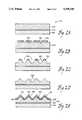
- FIGS. 1A-1Dthere are shown successive cross-sectional views of fabricating a field emitter device generally designated 10 according to a first embodiment of the present invention.
- a large area substrate 12 with a planar top surfaceis provided.
- Substrate 12is preferably glass, silicon or a metal although other materials can be used, the requirement being they provide a base upon which a plurality of emission tips can be fabricated.
- a continuous layer of a low work function material 14is disposed on substrate 12.
- a low work function material for the present inventionmust be 4.5 electron-volts or less, preferably 2.5 electron-volts or less.
- Diamondamorphic or nanocrystalline is the preferred low work function material; see, for instance, U.S. Pat. Nos. 5,199,918; 5,180,951; and 5,141,460; as well as U.S. application Ser. Nos. 08/147,700 filed Nov.
- suitable low work function materialsinclude tri-chromium mono-silicon (Cr 3 Si), tantalum-nitride (TAN), low work function compounds, metals (cesium) and cermets (e.g., tri-chromium mono-silicon silicon-dioxide (Cr 3 Si--SiO 2 ), trichromium mono-silicon magnesium-oxide (Cr 3 Si--MgO), gold silicon-dioxide (Au--SiO 2 ), and gold magnesium-oxide (Au--MgO)).
- Pr 3 Sitri-chromium mono-silicon
- TANtantalum-nitride
- cermetse.g., tri-chromium mono-silicon silicon-dioxide (Cr 3 Si--SiO 2 ), trichromium mono-silicon magnesium-oxide (Cr 3 Si--MgO), gold silicon-dioxide (Au--SiO 2 ), and gold magnesium-oxide
- Low work function material 14may be deposited on substrate 12, for instance, by sputtering, evaporation (including magnetically filtered cathode arc evaporation), laser deposition or chemical vapor deposition although the preferred technique depends on the particular material.
- evaporationincluding magnetically filtered cathode arc evaporation
- laser depositionor chemical vapor deposition although the preferred technique depends on the particular material.
- the preferred deposition techniques for diamond filmsare disclosed in U.S. Pat. Nos. 5,098,737 and 4,987,007.
- An optional adhesion layer 16such as 500 angstroms titanium, chromium, tantalum, titanium-tungsten or nickel-chromium can be deposited between substrate 12 and material 14.
- an etch mask 20 of randomly dispersed nucleiis deposited by physical vapor deposition on material 14. Discontinuities between the nuclei are formed in situ as mask 20 is deposited, as opposed to depositing a blanket layer and then selectively patterning openings such as by photolithography. More particularly, etch mask 20 is formed by depositing in situ a discontinuous layer of randomly located, spaced, discrete nuclei with discontinuities therebetween so as to form etch mask 20 on low work function material 14 thereby exposing some portions of the low work function material 14 (beneath the discontinuities) while covering other portions of material 14 (beneath the nuclei).
- mask 20serves to expose portions 22 of material 14 while covering portions 24 of material 14.
- Mask 20must be deposited by physical vapor deposition, such as by ionized metal cluster beams, liquid metal cluster beams, sputtering (including ion beam sputtering and magnetic ion beam sputtering) or evaporation.
- physical vapor depositionis distinct from chemical vapor deposition.
- particles moving toward a substrateeither fail to react or combine with a gas to form an oxide, nitride, carbide or the like.
- physical vapor deposition of a compound of a metal and a gas onto a surfaceis described in U.S. Pat. No. 5,196,102 which is incorporated herein by reference.
- Physical vapor depositiondoes not require chemical reduction of a vapor in contact with a substrate.
- physical vapor depositiondoes not encompass photodecomposition of a gaseous precursor (whether by blanket illumination through a photomask or by direct-write of a laser beam) or electron beam decomposition of a gas phase material at a substrate.
- physical vapor depositionavoids the need for highly uniform vapor composition and flow (which limits maximum substrate size) and toxic organo-metallic precursors, as typically required by chemical vapor deposition.
- suitable mask materialsinclude aluminum-oxide (Al 2 O 3 ), molybdenum, gold, and allotropic forms of carbon (including diamond and graphite). For example, diamond particles on the order of 50 angstroms diameter may be sprinkled on the substrate. It is noted that these mask materials are non-polymerized materials with relatively high melting points (i.e., above the melting point of aluminum and preferably above approximately 1000° C.) to assure properly shaped emission tips.
- Aluminum-oxidehas a very low sputtering yield (i.e., for an incoming atom how many atoms are etched off). A low sputtering yield in mask 20 relative to material 14 allows deep valleys to be etched in material 14 while using a relatively thin etch mask 20. Sputtering yields of various materials in argon are tabulated on p. 4-40 in Maissel and Glang.
- the discontinuities extending through the thickness of etch mask 20are formed in situ as physical vapor deposition occurs using techniques known to those having skill in the art.
- Maissel and Glang at p. 8-33report a nucleation and growth model in which a thin film having a thickness of 100 angstroms or less is generally discontinuous.
- Maissel and Glangreport experimental verification of this model at pp. 10-42 and 10-43.
- the nucleation siteis a random site where the first set of atoms/molecules reside during the initial formation of a thin film on a substrate. A majority (if not essentially all) of the nuclei grow as deposition occurs. Growth of the nuclei is three-dimensional although growth parallel to the substrate may be greater than growth normal to it.
- FIG. 21(a) on p. 10-42 of Maissel and Glangshows a large number of discrete three-dimensional nuclei in which the width of each nucleus is less than 1000 angstroms and each nucleus is spaced by a discontinuity of less than 1000 angstroms from the nearest adjacent nucleus.
- a thin film less than 10 angstroms thickmay fail to provide a reliable etch mask 20. Therefore, a discontinuous layer of etch mask between 10 and 100 angstroms thick is generally preferred.
- an etchis applied to the top of device 10 to remove portions of material 14 exposed by mask 20.
- Ion etching(which includes dry etching and plasma etching) is preferred and is illustrated herein.
- Wet chemical etching, for example,is not normally preferred due to undercutting of material 14 beneath the mask.
- a reactive etch(where a gas reacts with the surface to accelerate the etch) is normally unnecessary in the present invention.
- mask 20need not be erodible by the etch to form pyramid shaped emission tips since "shadowing" may occur whereby ions are deflected from the edge of the mask thereby accelerating the etch rate of exposed material spaced from the edges of the openings in the mask.
- the emission tipsmay be formed using a non-erodible etch mask.
- material 14, mask 20 and the ion etchare selected so that as the ion etch is applied mask 20 erodes slowly and material 14 etches at a greater rate than mask 20.
- material 14must etch at a greater rate than mask 20.
- vertical valleys 30 formed at the exposed portions 22extend partially through material 14, preferably between 100 angstroms and 1 micron deep, although if desired valleys 30 could extend completely through material 14.
- randomly located emission tips 32are formed between valleys 30.
- the distance between adjacent tipsexceeds the height of the tips for field enhancement purposes.
- the ion etchis continued so as to completely remove mask 20 and deepen the valleys. Emission tips 32 eventually assume a conical-pyramid shape with pointed tops due to preferential etching of the grain boundaries as has been previously demonstrated by heavy ion bombardment of copper films.
- the ion etchshould be carefully monitored to prevent completely removing one material thereby changing the work function of the material which remains on the substrate. For example, ion etching tantalum-nitride may remove all the nitride leaving a tantalum layer with too high a work function.
- the ion etchcan be halted before mask 20 is completely removed.
- the remainder of mask 20may then be removed by a second etch, such as wet chemical etching or dry etching, without removing additional material 14.
- a second etchsuch as wet chemical etching or dry etching.
- the resultant emission tipswould assume a rectangular-pyramid shape with relatively flat tops, as seen in FIG. 1C. This would not normally be preferred, however, since the conical-pyramid shape most enhances the electrical field distribution near the emission surface as field emission occurs.
- FIGS. 2A-2Ethere are shown successive cross-sectional views of fabricating a field emitter device 40 according a second embodiment of the present invention which overcomes the previously described difficulties for the embodiment in FIGS. 1A-1D at the cost of added complexity.
- a relatively thick (1000 angstroms to 3 microns) continuous layer of base material 44is sputter deposited on a substrate 42 (similar to substrate 12) with optional adhesion layer 46 (similar to adhesion layer 16) sandwiched therebetween.
- a preferred base material 44is an electrical conductor such as 3 micron thick copper, although resistive or semiconductive base materials are also suitable.
- a discontinuous layer of an etch mask 50(similar to mask 20) is deposited on base material 44 such that the discontinuities are formed in situ between randomly scattered nuclei as deposition occurs, thereby exposing portions 52 of material 44 while covering portions 54 of material 44.
- etch mask 50similar to mask 20
- an etch(illustrated as an ion etch) is applied to the top of device 40.
- Material 44, mask 50 and the ion etchare selected such that material 44 etches at a greater rate than mask 50, preferably at at least twice the etch rate.
- vertical valleys 56 formed at the exposed portions 52extend partially through material 44, and tip bases 58 are formed between valleys 56. If desired, valleys 56 could extend completely through material 44.
- 1000 electron-volt argon ions in the present illustrationthe large difference in sputtering yields of an aluminum-oxide mask 50 and copper base material 44 (0.04 and 3.2, respectively) produces very high aspect ratios for valleys 56.
- base tips 58assume a conical-pyramid shape.
- a coating of low work function material 60(similar to material 14) is deposited on base material 44, thereby forming randomly located conical-pyramid shaped emission tips 66 on base tips 58.
- An optional adhesion layer 68(similar to adhesion layer 16) can be sandwiched between materials 44 and 60 if desired.
- the ion etchcould be halted before completely removing mask 50, and a wet chemical etch or dry etch could remove the rest of mask 50 without removing additional base material 44 prior to depositing low work function material 60 thereon.
- the resultant base tips 58 and emission tips 66would assume the rectangular-pyramid shape seen in FIG. 2C which, as mentioned above, is not normally preferred.
- emission tips 66may include mask 50 sandwiched between materials 44 and 60 if desired.
- FIGS. 3 and 4elevational perspective views are shown of field emitter devices fabricated in accordance with FIGS. 1A-1D and 2A-2E, respectively.
- the emission tipscould assume circular or irregular pyramid shapes.
- the emission tipsmay be used as cold cathodes in a wide variety of systems and devices such as flat panel displays.
- the present inventionmay suitably comprise, consist of, or consist essentially of the forementioned process steps.
Landscapes
- Engineering & Computer Science (AREA)
- Manufacturing & Machinery (AREA)
- Cold Cathode And The Manufacture (AREA)
Abstract
Description
Claims (23)
Priority Applications (1)
| Application Number | Priority Date | Filing Date | Title |
|---|---|---|---|
| US08/232,790US5399238A (en) | 1991-11-07 | 1994-04-22 | Method of making field emission tips using physical vapor deposition of random nuclei as etch mask |
Applications Claiming Priority (3)
| Application Number | Priority Date | Filing Date | Title |
|---|---|---|---|
| US78922091A | 1991-11-07 | 1991-11-07 | |
| US08/052,958US5312514A (en) | 1991-11-07 | 1993-04-23 | Method of making a field emitter device using randomly located nuclei as an etch mask |
| US08/232,790US5399238A (en) | 1991-11-07 | 1994-04-22 | Method of making field emission tips using physical vapor deposition of random nuclei as etch mask |
Related Parent Applications (1)
| Application Number | Title | Priority Date | Filing Date |
|---|---|---|---|
| US08/052,958Continuation-In-PartUS5312514A (en) | 1991-02-11 | 1993-04-23 | Method of making a field emitter device using randomly located nuclei as an etch mask |
Publications (1)
| Publication Number | Publication Date |
|---|---|
| US5399238Atrue US5399238A (en) | 1995-03-21 |
Family
ID=26731298
Family Applications (1)
| Application Number | Title | Priority Date | Filing Date |
|---|---|---|---|
| US08/232,790Expired - LifetimeUS5399238A (en) | 1991-11-07 | 1994-04-22 | Method of making field emission tips using physical vapor deposition of random nuclei as etch mask |
Country Status (1)
| Country | Link |
|---|---|
| US (1) | US5399238A (en) |
Cited By (59)
| Publication number | Priority date | Publication date | Assignee | Title |
|---|---|---|---|---|
| US5536193A (en) | 1991-11-07 | 1996-07-16 | Microelectronics And Computer Technology Corporation | Method of making wide band gap field emitter |
| US5600200A (en) | 1992-03-16 | 1997-02-04 | Microelectronics And Computer Technology Corporation | Wire-mesh cathode |
| US5601966A (en) | 1993-11-04 | 1997-02-11 | Microelectronics And Computer Technology Corporation | Methods for fabricating flat panel display systems and components |
| US5612712A (en) | 1992-03-16 | 1997-03-18 | Microelectronics And Computer Technology Corporation | Diode structure flat panel display |
| US5628659A (en) | 1995-04-24 | 1997-05-13 | Microelectronics And Computer Corporation | Method of making a field emission electron source with random micro-tip structures |
| US5635081A (en) | 1994-07-12 | 1997-06-03 | Nec Corporation | Fabrication method of field-emission cold cathode |
| US5675216A (en) | 1992-03-16 | 1997-10-07 | Microelectronics And Computer Technololgy Corp. | Amorphic diamond film flat field emission cathode |
| US5679043A (en) | 1992-03-16 | 1997-10-21 | Microelectronics And Computer Technology Corporation | Method of making a field emitter |
| US5695658A (en)* | 1996-03-07 | 1997-12-09 | Micron Display Technology, Inc. | Non-photolithographic etch mask for submicron features |
| US5753130A (en)* | 1992-05-15 | 1998-05-19 | Micron Technology, Inc. | Method for forming a substantially uniform array of sharp tips |
| US5762773A (en)* | 1996-01-19 | 1998-06-09 | Micron Display Technology, Inc. | Method and system for manufacture of field emission display |
| US5763997A (en) | 1992-03-16 | 1998-06-09 | Si Diamond Technology, Inc. | Field emission display device |
| US5817373A (en)* | 1996-12-12 | 1998-10-06 | Micron Display Technology, Inc. | Dry dispense of particles for microstructure fabrication |
| US5841219A (en)* | 1993-09-22 | 1998-11-24 | University Of Utah Research Foundation | Microminiature thermionic vacuum tube |
| US5844252A (en)* | 1993-09-24 | 1998-12-01 | Sumitomo Electric Industries, Ltd. | Field emission devices having diamond field emitter, methods for making same, and methods for fabricating porous diamond |
| US5857882A (en)* | 1996-02-27 | 1999-01-12 | Sandia Corporation | Processing of materials for uniform field emission |
| US5888113A (en)* | 1997-03-27 | 1999-03-30 | Universities Research Association, Inc. | Process for making a cesiated diamond film field emitter and field emitter formed therefrom |
| US5955828A (en)* | 1996-10-16 | 1999-09-21 | University Of Utah Research Foundation | Thermionic optical emission device |
| US6008577A (en)* | 1996-01-18 | 1999-12-28 | Micron Technology, Inc. | Flat panel display with magnetic focusing layer |
| US6037104A (en)* | 1998-09-01 | 2000-03-14 | Micron Display Technology, Inc. | Methods of forming semiconductor devices and methods of forming field emission displays |
| US6051149A (en)* | 1998-03-12 | 2000-04-18 | Micron Technology, Inc. | Coated beads and process utilizing such beads for forming an etch mask having a discontinuous regular pattern |
| US6060219A (en)* | 1998-05-21 | 2000-05-09 | Micron Technology, Inc. | Methods of forming electron emitters, surface conduction electron emitters and field emission display assemblies |
| US6068750A (en)* | 1996-01-19 | 2000-05-30 | Micron Technology, Inc. | Faceplates having black matrix material |
| US6083767A (en)* | 1998-05-26 | 2000-07-04 | Micron Technology, Inc. | Method of patterning a semiconductor device |
| US6114256A (en)* | 1995-08-18 | 2000-09-05 | California Institute Of Technology | Stable metallization for diamond and other materials |
| US6127773A (en) | 1992-03-16 | 2000-10-03 | Si Diamond Technology, Inc. | Amorphic diamond film flat field emission cathode |
| US6171164B1 (en) | 1998-02-19 | 2001-01-09 | Micron Technology, Inc. | Method for forming uniform sharp tips for use in a field emission array |
| US6174449B1 (en) | 1998-05-14 | 2001-01-16 | Micron Technology, Inc. | Magnetically patterned etch mask |
| US6207578B1 (en) | 1999-02-19 | 2001-03-27 | Micron Technology, Inc. | Methods of forming patterned constructions, methods of patterning semiconductive substrates, and methods of forming field emission displays |
| US6228538B1 (en) | 1998-08-28 | 2001-05-08 | Micron Technology, Inc. | Mask forming methods and field emission display emitter mask forming methods |
| US6296740B1 (en)* | 1995-04-24 | 2001-10-02 | Si Diamond Technology, Inc. | Pretreatment process for a surface texturing process |
| US6309554B1 (en)* | 1998-06-12 | 2001-10-30 | The University Of Tokyo | Method for producing needle diamond-type structure |
| US6350388B1 (en) | 1999-08-19 | 2002-02-26 | Micron Technology, Inc. | Method for patterning high density field emitter tips |
| US6372405B1 (en) | 1999-02-17 | 2002-04-16 | Micron Technology, Inc. | Method, article and composition for limiting particle aggregation in a mask deposited by a colloidal suspension |
| US20020113536A1 (en)* | 1999-03-01 | 2002-08-22 | Ammar Derraa | Field emitter display (FED) assemblies and methods of forming field emitter display (FED) assemblies |
| US20020135387A1 (en)* | 1998-04-03 | 2002-09-26 | Susumu Kasukabe | Probing device and manufacturing method thereof, as well as testing apparatus and manufacturing method of semiconductor with use thereof |
| WO2002047176A3 (en)* | 2000-12-07 | 2002-12-05 | Ibm | Enhanced interface thermoelectric coolers |
| US6514674B1 (en)* | 1999-03-11 | 2003-02-04 | Canon Kabushiki Kaisha | Method of forming an optical element |
| US6524874B1 (en) | 1998-08-05 | 2003-02-25 | Micron Technology, Inc. | Methods of forming field emission tips using deposited particles as an etch mask |
| USD472529S1 (en) | 2002-01-17 | 2003-04-01 | Sony Corporation | Semiconductor element |
| USD472531S1 (en) | 2002-06-25 | 2003-04-01 | Sony Corporation | Semiconductor element |
| US20030168428A1 (en)* | 2001-02-21 | 2003-09-11 | Akira Kouchiyama | Method for producing original record of optical recording medium |
| US6629869B1 (en) | 1992-03-16 | 2003-10-07 | Si Diamond Technology, Inc. | Method of making flat panel displays having diamond thin film cathode |
| USD485242S1 (en) | 2002-01-17 | 2004-01-13 | Sony Corporation | Semiconductor element |
| US6762543B1 (en)* | 1996-06-25 | 2004-07-13 | Vanderbilt University | Diamond diode devices with a diamond microtip emitter |
| US6780491B1 (en) | 1996-12-12 | 2004-08-24 | Micron Technology, Inc. | Microstructures including hydrophilic particles |
| US6824855B1 (en) | 1998-03-12 | 2004-11-30 | Micron Technology, Inc. | Coated beads and process utilizing such beads for forming an etch mask having a discontinuous regular pattern |
| US6841249B2 (en)* | 2000-02-09 | 2005-01-11 | Universite Pierre Et Marie Curie | Method of a diamond surface and corresponding diamond surface |
| US20050016575A1 (en)* | 2003-06-13 | 2005-01-27 | Nalin Kumar | Field emission based thermoelectric device |
| US20050269286A1 (en)* | 2004-06-08 | 2005-12-08 | Manish Sharma | Method of fabricating a nano-wire |
| US20060202392A1 (en)* | 2005-03-14 | 2006-09-14 | Agency For Science, Technology And Research | Tunable mask apparatus and process |
| US20070184257A1 (en)* | 2006-02-09 | 2007-08-09 | Isoflux, Inc. | Formation of nanoscale surfaces for the atttachment of biological materials |
| US20080299337A1 (en)* | 2006-02-09 | 2008-12-04 | Isoflux, Inc. | Method for the formation of surfaces on the inside of medical devices |
| EP2714190A4 (en)* | 2011-06-03 | 2014-05-21 | Univ Melbourne | ELECTRODE AND CROSSWAY FOR MEDICAL DEVICE APPLICATIONS |
| US8866068B2 (en) | 2012-12-27 | 2014-10-21 | Schlumberger Technology Corporation | Ion source with cathode having an array of nano-sized projections |
| US20140322918A1 (en)* | 2008-07-01 | 2014-10-30 | Alcatel-Lucent Usa Inc. | Micro-posts having improved uniformity and a method of manufacture thereof |
| US9136794B2 (en) | 2011-06-22 | 2015-09-15 | Research Triangle Institute, International | Bipolar microelectronic device |
| US9852870B2 (en)* | 2011-05-23 | 2017-12-26 | Corporation For National Research Initiatives | Method for the fabrication of electron field emission devices including carbon nanotube field electron emisson devices |
| CN111362225A (en)* | 2020-03-17 | 2020-07-03 | 中国科学院半导体研究所 | Nano needle tip structure, composite structure and preparation method thereof |
Citations (37)
| Publication number | Priority date | Publication date | Assignee | Title |
|---|---|---|---|---|
| US2959704A (en)* | 1958-10-09 | 1960-11-08 | Gen Electric | Overvoltage protective device |
| US3625758A (en)* | 1966-02-22 | 1971-12-07 | Photocircuits Corp | Base material and method for the manufacture of printed circuits |
| US3894332A (en)* | 1972-02-11 | 1975-07-15 | Westinghouse Electric Corp | Solid state radiation sensitive field electron emitter and methods of fabrication thereof |
| US3947716A (en)* | 1973-08-27 | 1976-03-30 | The United States Of America As Represented By The Secretary Of The Army | Field emission tip and process for making same |
| US3970887A (en)* | 1974-06-19 | 1976-07-20 | Micro-Bit Corporation | Micro-structure field emission electron source |
| US3998678A (en)* | 1973-03-22 | 1976-12-21 | Hitachi, Ltd. | Method of manufacturing thin-film field-emission electron source |
| US4115228A (en)* | 1975-08-13 | 1978-09-19 | Massachusetts Institute Of Technology | Method of making secondary-electron emitters |
| US4139773A (en)* | 1977-11-04 | 1979-02-13 | Oregon Graduate Center | Method and apparatus for producing bright high resolution ion beams |
| US4307507A (en)* | 1980-09-10 | 1981-12-29 | The United States Of America As Represented By The Secretary Of The Navy | Method of manufacturing a field-emission cathode structure |
| US4350926A (en)* | 1980-07-28 | 1982-09-21 | The United States Of America As Represented By The Secretary Of The Army | Hollow beam electron source |
| US4465551A (en)* | 1980-05-07 | 1984-08-14 | Horwitz Christopher M | Graded microstructured layers formed by vacuum etching |
| US4566937A (en)* | 1984-10-10 | 1986-01-28 | The United States Of America As Represented By The United States Department Of Energy | Electron beam enhanced surface modification for making highly resolved structures |
| US4612085A (en)* | 1985-04-10 | 1986-09-16 | Texas Instruments Incorporated | Photochemical patterning |
| US4663559A (en)* | 1982-09-17 | 1987-05-05 | Christensen Alton O | Field emission device |
| US4685996A (en)* | 1986-10-14 | 1987-08-11 | Busta Heinz H | Method of making micromachined refractory metal field emitters |
| US4764485A (en)* | 1987-01-05 | 1988-08-16 | General Electric Company | Method for producing via holes in polymer dielectrics |
| US4806202A (en)* | 1987-10-05 | 1989-02-21 | Intel Corporation | Field enhanced tunnel oxide on treated substrates |
| US4855636A (en)* | 1987-10-08 | 1989-08-08 | Busta Heinz H | Micromachined cold cathode vacuum tube device and method of making |
| US4895735A (en)* | 1988-03-01 | 1990-01-23 | Texas Instruments Incorporated | Radiation induced pattern deposition |
| US4933108A (en)* | 1978-04-13 | 1990-06-12 | Soeredal Sven G | Emitter for field emission and method of making same |
| US4943343A (en)* | 1989-08-14 | 1990-07-24 | Zaher Bardai | Self-aligned gate process for fabricating field emitter arrays |
| US4964946A (en)* | 1990-02-02 | 1990-10-23 | The United States Of America As Represented By The Secretary Of The Navy | Process for fabricating self-aligned field emitter arrays |
| US4968382A (en)* | 1989-01-18 | 1990-11-06 | The General Electric Company, P.L.C. | Electronic devices |
| US4973378A (en)* | 1989-03-01 | 1990-11-27 | The General Electric Company, P.L.C. | Method of making electronic devices |
| US5019003A (en)* | 1989-09-29 | 1991-05-28 | Motorola, Inc. | Field emission device having preformed emitters |
| US5035768A (en)* | 1989-11-14 | 1991-07-30 | Intel Corporation | Novel etch back process for tungsten contact/via filling |
| US5104684A (en)* | 1990-05-25 | 1992-04-14 | Massachusetts Institute Of Technology | Ion beam induced deposition of metals |
| US5129850A (en)* | 1991-08-20 | 1992-07-14 | Motorola, Inc. | Method of making a molded field emission electron emitter employing a diamond coating |
| US5141460A (en)* | 1991-08-20 | 1992-08-25 | Jaskie James E | Method of making a field emission electron source employing a diamond coating |
| US5147823A (en)* | 1988-09-20 | 1992-09-15 | Sony Corporation | Method for forming an ultrafine metal pattern using an electron beam |
| US5156997A (en)* | 1991-02-11 | 1992-10-20 | Microelectronics And Computer Technology Corporation | Method of making semiconductor bonding bumps using metal cluster ion deposition |
| US5180951A (en)* | 1992-02-05 | 1993-01-19 | Motorola, Inc. | Electron device electron source including a polycrystalline diamond |
| US5185178A (en)* | 1988-08-29 | 1993-02-09 | Minnesota Mining And Manufacturing Company | Method of forming an array of densely packed discrete metal microspheres |
| US5196102A (en)* | 1991-08-08 | 1993-03-23 | Microelectronics And Computer Technology Corporation | Method and apparatus for applying a compound of a metal and a gas onto a surface |
| US5220725A (en)* | 1991-04-09 | 1993-06-22 | Northeastern University | Micro-emitter-based low-contact-force interconnection device |
| US5244538A (en)* | 1991-07-26 | 1993-09-14 | Microelectronics And Computer Technology Corporation | Method of patterning metal on a substrate using direct-write deposition of a mask |
| US5312514A (en)* | 1991-11-07 | 1994-05-17 | Microelectronics And Computer Technology Corporation | Method of making a field emitter device using randomly located nuclei as an etch mask |
- 1994
- 1994-04-22USUS08/232,790patent/US5399238A/ennot_activeExpired - Lifetime
Patent Citations (38)
| Publication number | Priority date | Publication date | Assignee | Title |
|---|---|---|---|---|
| US2959704A (en)* | 1958-10-09 | 1960-11-08 | Gen Electric | Overvoltage protective device |
| US3625758A (en)* | 1966-02-22 | 1971-12-07 | Photocircuits Corp | Base material and method for the manufacture of printed circuits |
| US3894332A (en)* | 1972-02-11 | 1975-07-15 | Westinghouse Electric Corp | Solid state radiation sensitive field electron emitter and methods of fabrication thereof |
| US3998678A (en)* | 1973-03-22 | 1976-12-21 | Hitachi, Ltd. | Method of manufacturing thin-film field-emission electron source |
| US3947716A (en)* | 1973-08-27 | 1976-03-30 | The United States Of America As Represented By The Secretary Of The Army | Field emission tip and process for making same |
| US3970887A (en)* | 1974-06-19 | 1976-07-20 | Micro-Bit Corporation | Micro-structure field emission electron source |
| US4115228A (en)* | 1975-08-13 | 1978-09-19 | Massachusetts Institute Of Technology | Method of making secondary-electron emitters |
| US4139773A (en)* | 1977-11-04 | 1979-02-13 | Oregon Graduate Center | Method and apparatus for producing bright high resolution ion beams |
| US4933108A (en)* | 1978-04-13 | 1990-06-12 | Soeredal Sven G | Emitter for field emission and method of making same |
| US4465551A (en)* | 1980-05-07 | 1984-08-14 | Horwitz Christopher M | Graded microstructured layers formed by vacuum etching |
| US4350926A (en)* | 1980-07-28 | 1982-09-21 | The United States Of America As Represented By The Secretary Of The Army | Hollow beam electron source |
| US4307507A (en)* | 1980-09-10 | 1981-12-29 | The United States Of America As Represented By The Secretary Of The Navy | Method of manufacturing a field-emission cathode structure |
| US4663559A (en)* | 1982-09-17 | 1987-05-05 | Christensen Alton O | Field emission device |
| US4566937A (en)* | 1984-10-10 | 1986-01-28 | The United States Of America As Represented By The United States Department Of Energy | Electron beam enhanced surface modification for making highly resolved structures |
| US4612085A (en)* | 1985-04-10 | 1986-09-16 | Texas Instruments Incorporated | Photochemical patterning |
| US4685996A (en)* | 1986-10-14 | 1987-08-11 | Busta Heinz H | Method of making micromachined refractory metal field emitters |
| US4764485A (en)* | 1987-01-05 | 1988-08-16 | General Electric Company | Method for producing via holes in polymer dielectrics |
| US4806202A (en)* | 1987-10-05 | 1989-02-21 | Intel Corporation | Field enhanced tunnel oxide on treated substrates |
| US4855636A (en)* | 1987-10-08 | 1989-08-08 | Busta Heinz H | Micromachined cold cathode vacuum tube device and method of making |
| US4895735A (en)* | 1988-03-01 | 1990-01-23 | Texas Instruments Incorporated | Radiation induced pattern deposition |
| US5185178A (en)* | 1988-08-29 | 1993-02-09 | Minnesota Mining And Manufacturing Company | Method of forming an array of densely packed discrete metal microspheres |
| US5147823A (en)* | 1988-09-20 | 1992-09-15 | Sony Corporation | Method for forming an ultrafine metal pattern using an electron beam |
| US4968382A (en)* | 1989-01-18 | 1990-11-06 | The General Electric Company, P.L.C. | Electronic devices |
| US4973378A (en)* | 1989-03-01 | 1990-11-27 | The General Electric Company, P.L.C. | Method of making electronic devices |
| US4943343A (en)* | 1989-08-14 | 1990-07-24 | Zaher Bardai | Self-aligned gate process for fabricating field emitter arrays |
| US5019003A (en)* | 1989-09-29 | 1991-05-28 | Motorola, Inc. | Field emission device having preformed emitters |
| US5035768A (en)* | 1989-11-14 | 1991-07-30 | Intel Corporation | Novel etch back process for tungsten contact/via filling |
| US4964946A (en)* | 1990-02-02 | 1990-10-23 | The United States Of America As Represented By The Secretary Of The Navy | Process for fabricating self-aligned field emitter arrays |
| US5104684A (en)* | 1990-05-25 | 1992-04-14 | Massachusetts Institute Of Technology | Ion beam induced deposition of metals |
| US5156997A (en)* | 1991-02-11 | 1992-10-20 | Microelectronics And Computer Technology Corporation | Method of making semiconductor bonding bumps using metal cluster ion deposition |
| US5290732A (en)* | 1991-02-11 | 1994-03-01 | Microelectronics And Computer Technology Corporation | Process for making semiconductor electrode bumps by metal cluster ion deposition and etching |
| US5220725A (en)* | 1991-04-09 | 1993-06-22 | Northeastern University | Micro-emitter-based low-contact-force interconnection device |
| US5244538A (en)* | 1991-07-26 | 1993-09-14 | Microelectronics And Computer Technology Corporation | Method of patterning metal on a substrate using direct-write deposition of a mask |
| US5196102A (en)* | 1991-08-08 | 1993-03-23 | Microelectronics And Computer Technology Corporation | Method and apparatus for applying a compound of a metal and a gas onto a surface |
| US5129850A (en)* | 1991-08-20 | 1992-07-14 | Motorola, Inc. | Method of making a molded field emission electron emitter employing a diamond coating |
| US5141460A (en)* | 1991-08-20 | 1992-08-25 | Jaskie James E | Method of making a field emission electron source employing a diamond coating |
| US5312514A (en)* | 1991-11-07 | 1994-05-17 | Microelectronics And Computer Technology Corporation | Method of making a field emitter device using randomly located nuclei as an etch mask |
| US5180951A (en)* | 1992-02-05 | 1993-01-19 | Motorola, Inc. | Electron device electron source including a polycrystalline diamond |
Non-Patent Citations (8)
| Title |
|---|
| Cade and Lee, "Vacuum Microelectronics", GEC J. Res. Inc., Marconi Rev., 7(3), 129(1990). |
| Cade and Lee, Vacuum Microelectronics , GEC J. Res. Inc., Marconi Rev., 7(3), 129(1990).* |
| Horwitz, "A new vacuum-etched high-transmittance (antireflection)film", Applied Physics Letters vol. 36, No. 9, May 1, 1980, pp. 727-730. |
| Horwitz, A new vacuum etched high transmittance (antireflection)film , Applied Physics Letters vol. 36, No. 9, May 1, 1980, pp. 727 730.* |
| Horwitz, McPhedran and Beunan, "Interference and diffraction in globular metal films", Journal of the Optical Society of America, vol. 68, No. 8, Aug. 1978, pp. 1023-1031. |
| Horwitz, McPhedran and Beunan, Interference and diffraction in globular metal films , Journal of the Optical Society of America, vol. 68, No. 8, Aug. 1978, pp. 1023 1031.* |
| Maissel and Glang, Handbook of Thin Film Technology, 1983 Reissue, McGraw Hill, New York, NY.* |
| Maissel and Glang, Handbook of Thin Film Technology, 1983 Reissue, McGraw-Hill, New York, NY. |
Cited By (110)
| Publication number | Priority date | Publication date | Assignee | Title |
|---|---|---|---|---|
| US5861707A (en) | 1991-11-07 | 1999-01-19 | Si Diamond Technology, Inc. | Field emitter with wide band gap emission areas and method of using |
| US5536193A (en) | 1991-11-07 | 1996-07-16 | Microelectronics And Computer Technology Corporation | Method of making wide band gap field emitter |
| US5675216A (en) | 1992-03-16 | 1997-10-07 | Microelectronics And Computer Technololgy Corp. | Amorphic diamond film flat field emission cathode |
| US5703435A (en) | 1992-03-16 | 1997-12-30 | Microelectronics & Computer Technology Corp. | Diamond film flat field emission cathode |
| US6127773A (en) | 1992-03-16 | 2000-10-03 | Si Diamond Technology, Inc. | Amorphic diamond film flat field emission cathode |
| US5600200A (en) | 1992-03-16 | 1997-02-04 | Microelectronics And Computer Technology Corporation | Wire-mesh cathode |
| US5763997A (en) | 1992-03-16 | 1998-06-09 | Si Diamond Technology, Inc. | Field emission display device |
| US6629869B1 (en) | 1992-03-16 | 2003-10-07 | Si Diamond Technology, Inc. | Method of making flat panel displays having diamond thin film cathode |
| US5612712A (en) | 1992-03-16 | 1997-03-18 | Microelectronics And Computer Technology Corporation | Diode structure flat panel display |
| US5679043A (en) | 1992-03-16 | 1997-10-21 | Microelectronics And Computer Technology Corporation | Method of making a field emitter |
| US5686791A (en) | 1992-03-16 | 1997-11-11 | Microelectronics And Computer Technology Corp. | Amorphic diamond film flat field emission cathode |
| US6423239B1 (en) | 1992-05-15 | 2002-07-23 | Micron Technology, Inc. | Methods of making an etch mask and etching a substrate using said etch mask |
| US5753130A (en)* | 1992-05-15 | 1998-05-19 | Micron Technology, Inc. | Method for forming a substantially uniform array of sharp tips |
| US6165374A (en)* | 1992-05-15 | 2000-12-26 | Micron Technology, Inc. | Method of forming an array of emitter tips |
| US6080325A (en)* | 1992-05-15 | 2000-06-27 | Micron Technology, Inc. | Method of etching a substrate and method of forming a plurality of emitter tips |
| US6126845A (en)* | 1992-05-15 | 2000-10-03 | Micron Technology, Inc. | Method of forming an array of emmitter tips |
| US5841219A (en)* | 1993-09-22 | 1998-11-24 | University Of Utah Research Foundation | Microminiature thermionic vacuum tube |
| US5844252A (en)* | 1993-09-24 | 1998-12-01 | Sumitomo Electric Industries, Ltd. | Field emission devices having diamond field emitter, methods for making same, and methods for fabricating porous diamond |
| US5652083A (en) | 1993-11-04 | 1997-07-29 | Microelectronics And Computer Technology Corporation | Methods for fabricating flat panel display systems and components |
| US5601966A (en) | 1993-11-04 | 1997-02-11 | Microelectronics And Computer Technology Corporation | Methods for fabricating flat panel display systems and components |
| US5614353A (en) | 1993-11-04 | 1997-03-25 | Si Diamond Technology, Inc. | Methods for fabricating flat panel display systems and components |
| US5635081A (en) | 1994-07-12 | 1997-06-03 | Nec Corporation | Fabrication method of field-emission cold cathode |
| US6296740B1 (en)* | 1995-04-24 | 2001-10-02 | Si Diamond Technology, Inc. | Pretreatment process for a surface texturing process |
| US5628659A (en) | 1995-04-24 | 1997-05-13 | Microelectronics And Computer Corporation | Method of making a field emission electron source with random micro-tip structures |
| US6613204B2 (en) | 1995-04-24 | 2003-09-02 | Si Diamond Technology, Inc. | Pretreatment process for a surface texturing process |
| US6114256A (en)* | 1995-08-18 | 2000-09-05 | California Institute Of Technology | Stable metallization for diamond and other materials |
| US6008577A (en)* | 1996-01-18 | 1999-12-28 | Micron Technology, Inc. | Flat panel display with magnetic focusing layer |
| US6296750B1 (en) | 1996-01-19 | 2001-10-02 | Micron Technology, Inc. | Composition including black matrix material |
| US6596141B2 (en) | 1996-01-19 | 2003-07-22 | Micron Technology, Inc. | Field emission display having matrix material |
| US6068750A (en)* | 1996-01-19 | 2000-05-30 | Micron Technology, Inc. | Faceplates having black matrix material |
| US6224730B1 (en) | 1996-01-19 | 2001-05-01 | Micron Technology, Inc. | Field emission display having black matrix material |
| US6540898B2 (en) | 1996-01-19 | 2003-04-01 | Micron Technology, Inc. | Method and system for manufacture of field emission display |
| US6117294A (en)* | 1996-01-19 | 2000-09-12 | Micron Technology, Inc. | Black matrix material and methods related thereto |
| US5762773A (en)* | 1996-01-19 | 1998-06-09 | Micron Display Technology, Inc. | Method and system for manufacture of field emission display |
| US5857882A (en)* | 1996-02-27 | 1999-01-12 | Sandia Corporation | Processing of materials for uniform field emission |
| US5695658A (en)* | 1996-03-07 | 1997-12-09 | Micron Display Technology, Inc. | Non-photolithographic etch mask for submicron features |
| US7256535B2 (en) | 1996-06-25 | 2007-08-14 | Vanderbilt University | Diamond triode devices with a diamond microtip emitter |
| US6762543B1 (en)* | 1996-06-25 | 2004-07-13 | Vanderbilt University | Diamond diode devices with a diamond microtip emitter |
| US5955828A (en)* | 1996-10-16 | 1999-09-21 | University Of Utah Research Foundation | Thermionic optical emission device |
| US6110394A (en)* | 1996-12-12 | 2000-08-29 | Micron Technology, Inc. | Dry dispense of particles to form a fabrication mask |
| US6780491B1 (en) | 1996-12-12 | 2004-08-24 | Micron Technology, Inc. | Microstructures including hydrophilic particles |
| US5817373A (en)* | 1996-12-12 | 1998-10-06 | Micron Display Technology, Inc. | Dry dispense of particles for microstructure fabrication |
| US5888113A (en)* | 1997-03-27 | 1999-03-30 | Universities Research Association, Inc. | Process for making a cesiated diamond film field emitter and field emitter formed therefrom |
| US6171164B1 (en) | 1998-02-19 | 2001-01-09 | Micron Technology, Inc. | Method for forming uniform sharp tips for use in a field emission array |
| US6689282B2 (en) | 1998-02-19 | 2004-02-10 | Micron Technology, Inc. | Method for forming uniform sharp tips for use in a field emission array |
| US6660173B2 (en) | 1998-02-19 | 2003-12-09 | Micron Technology, Inc. | Method for forming uniform sharp tips for use in a field emission array |
| US6753643B2 (en) | 1998-02-19 | 2004-06-22 | Micron Technology, Inc. | Method for forming uniform sharp tips for use in a field emission array |
| US6461526B1 (en) | 1998-02-19 | 2002-10-08 | Micron Technology, Inc. | Method for forming uniform sharp tips for use in a field emission array |
| US6416376B1 (en) | 1998-02-19 | 2002-07-09 | Micron Technology, Inc. | Method for forming uniform sharp tips for use in a field emission array |
| US20040033691A1 (en)* | 1998-03-12 | 2004-02-19 | Frendt Joel M. | Coated beads and process utilizing such beads for forming an etch mask having a discontinuous regular pattern |
| US6464888B1 (en) | 1998-03-12 | 2002-10-15 | Micron Technology, Inc. | Coated beads and process utilizing such beads for forming an etch mask having a discontinuous regular pattern |
| US6676845B2 (en) | 1998-03-12 | 2004-01-13 | Micron Technology, Inc. | Coated beads and process utilizing such beads for forming an etch mask having a discontinuous regular pattern |
| US6824855B1 (en) | 1998-03-12 | 2004-11-30 | Micron Technology, Inc. | Coated beads and process utilizing such beads for forming an etch mask having a discontinuous regular pattern |
| US6706386B2 (en) | 1998-03-12 | 2004-03-16 | Micron Technology, Inc. | Coated beads for forming an etch mask having a discontinuous regular pattern |
| US6562438B1 (en) | 1998-03-12 | 2003-05-13 | Micron Technology, Inc. | Coated beads and process utilizing such beads for forming an etch mask having a discontinuous regular pattern |
| US7029592B2 (en) | 1998-03-12 | 2006-04-18 | Micron Technology, Inc. | Coated beads and process utilizing such beads for forming an etch mask having a discontinuous regular pattern |
| US6051149A (en)* | 1998-03-12 | 2000-04-18 | Micron Technology, Inc. | Coated beads and process utilizing such beads for forming an etch mask having a discontinuous regular pattern |
| US6900646B2 (en) | 1998-04-03 | 2005-05-31 | Hitachi, Ltd. | Probing device and manufacturing method thereof, as well as testing apparatus and manufacturing method of semiconductor with use thereof |
| US20020135387A1 (en)* | 1998-04-03 | 2002-09-26 | Susumu Kasukabe | Probing device and manufacturing method thereof, as well as testing apparatus and manufacturing method of semiconductor with use thereof |
| US6617863B1 (en)* | 1998-04-03 | 2003-09-09 | Hitachi, Ltd. | Probing device and manufacturing method thereof, as well as testing apparatus and manufacturing method of semiconductor with use thereof |
| US6174449B1 (en) | 1998-05-14 | 2001-01-16 | Micron Technology, Inc. | Magnetically patterned etch mask |
| US6060219A (en)* | 1998-05-21 | 2000-05-09 | Micron Technology, Inc. | Methods of forming electron emitters, surface conduction electron emitters and field emission display assemblies |
| US6083767A (en)* | 1998-05-26 | 2000-07-04 | Micron Technology, Inc. | Method of patterning a semiconductor device |
| US6309554B1 (en)* | 1998-06-12 | 2001-10-30 | The University Of Tokyo | Method for producing needle diamond-type structure |
| US6524874B1 (en) | 1998-08-05 | 2003-02-25 | Micron Technology, Inc. | Methods of forming field emission tips using deposited particles as an etch mask |
| US6537728B2 (en) | 1998-08-28 | 2003-03-25 | Micron Technology, Inc. | Structures, lithographic mask forming solutions, mask forming methods, field emission display emitter mask forming methods, and methods of forming plural field emission display emitters |
| US6682873B2 (en) | 1998-08-28 | 2004-01-27 | Micron Technology, Inc. | Semiconductive substrate processing methods and methods of processing a semiconductive substrate |
| US6458515B2 (en) | 1998-08-28 | 2002-10-01 | Micron Technology, Inc. | Structures, lithographic mask forming solutions, mask forming methods, field emission display emitter mask forming methods, and methods of forming plural field emission display emitters |
| US6573023B2 (en) | 1998-08-28 | 2003-06-03 | Micron Technology, Inc. | Structures and structure forming methods |
| US6586144B2 (en) | 1998-08-28 | 2003-07-01 | Micron Technology, Inc. | Mask forming methods and a field emission display emitter mask forming method |
| US6228538B1 (en) | 1998-08-28 | 2001-05-08 | Micron Technology, Inc. | Mask forming methods and field emission display emitter mask forming methods |
| US6338938B1 (en) | 1998-09-01 | 2002-01-15 | Micron Technology, Inc. | Methods of forming semiconductor devices and methods of forming field emission displays |
| US6037104A (en)* | 1998-09-01 | 2000-03-14 | Micron Display Technology, Inc. | Methods of forming semiconductor devices and methods of forming field emission displays |
| US6372405B1 (en) | 1999-02-17 | 2002-04-16 | Micron Technology, Inc. | Method, article and composition for limiting particle aggregation in a mask deposited by a colloidal suspension |
| US6495296B1 (en) | 1999-02-17 | 2002-12-17 | Micron Technology, Inc. | Method for limiting particle aggregation in a mask deposited by a colloidal suspension |
| US6372404B1 (en) | 1999-02-17 | 2002-04-16 | Micron Technology, Inc. | Method, article and composition for limiting particle aggregation in a mask deposited by a colloidal suspension |
| US6428943B1 (en) | 1999-02-17 | 2002-08-06 | Micron Technology, Inc. | Method, article and composition for limiting particle aggregation in a mask deposited by a colloidal suspension |
| US6420086B1 (en) | 1999-02-19 | 2002-07-16 | Micron Technology, Inc. | Methods of forming patterned constructions, methods of patterning semiconductive substrates, and methods of forming field emission displays |
| US6207578B1 (en) | 1999-02-19 | 2001-03-27 | Micron Technology, Inc. | Methods of forming patterned constructions, methods of patterning semiconductive substrates, and methods of forming field emission displays |
| US20030001489A1 (en)* | 1999-03-01 | 2003-01-02 | Ammar Derraa | Field emitter display assembly having resistor layer |
| US6790114B2 (en) | 1999-03-01 | 2004-09-14 | Micron Technology, Inc. | Methods of forming field emitter display (FED) assemblies |
| US6822386B2 (en) | 1999-03-01 | 2004-11-23 | Micron Technology, Inc. | Field emitter display assembly having resistor layer |
| US20020113536A1 (en)* | 1999-03-01 | 2002-08-22 | Ammar Derraa | Field emitter display (FED) assemblies and methods of forming field emitter display (FED) assemblies |
| US6514674B1 (en)* | 1999-03-11 | 2003-02-04 | Canon Kabushiki Kaisha | Method of forming an optical element |
| US6679998B2 (en) | 1999-08-19 | 2004-01-20 | Micron Technology, Inc. | Method for patterning high density field emitter tips |
| US6350388B1 (en) | 1999-08-19 | 2002-02-26 | Micron Technology, Inc. | Method for patterning high density field emitter tips |
| US6464890B2 (en) | 1999-08-19 | 2002-10-15 | Micron Technology, Inc. | Method for patterning high density field emitter tips |
| US6841249B2 (en)* | 2000-02-09 | 2005-01-11 | Universite Pierre Et Marie Curie | Method of a diamond surface and corresponding diamond surface |
| US6740600B2 (en) | 2000-12-07 | 2004-05-25 | International Business Machines Corporation | Enhanced interface thermoelectric coolers with all-metals tips |
| WO2002047176A3 (en)* | 2000-12-07 | 2002-12-05 | Ibm | Enhanced interface thermoelectric coolers |
| US20030168428A1 (en)* | 2001-02-21 | 2003-09-11 | Akira Kouchiyama | Method for producing original record of optical recording medium |
| USD472529S1 (en) | 2002-01-17 | 2003-04-01 | Sony Corporation | Semiconductor element |
| USD485242S1 (en) | 2002-01-17 | 2004-01-13 | Sony Corporation | Semiconductor element |
| USD472531S1 (en) | 2002-06-25 | 2003-04-01 | Sony Corporation | Semiconductor element |
| US20050016575A1 (en)* | 2003-06-13 | 2005-01-27 | Nalin Kumar | Field emission based thermoelectric device |
| US20050269286A1 (en)* | 2004-06-08 | 2005-12-08 | Manish Sharma | Method of fabricating a nano-wire |
| US20060202392A1 (en)* | 2005-03-14 | 2006-09-14 | Agency For Science, Technology And Research | Tunable mask apparatus and process |
| US20070184257A1 (en)* | 2006-02-09 | 2007-08-09 | Isoflux, Inc. | Formation of nanoscale surfaces for the atttachment of biological materials |
| EP1826293A1 (en)* | 2006-02-09 | 2007-08-29 | Isoflux, Inc. | Formation of nanoscale surfaces for the attachment of biological materials |
| US20080299337A1 (en)* | 2006-02-09 | 2008-12-04 | Isoflux, Inc. | Method for the formation of surfaces on the inside of medical devices |
| US20140322918A1 (en)* | 2008-07-01 | 2014-10-30 | Alcatel-Lucent Usa Inc. | Micro-posts having improved uniformity and a method of manufacture thereof |
| US9852870B2 (en)* | 2011-05-23 | 2017-12-26 | Corporation For National Research Initiatives | Method for the fabrication of electron field emission devices including carbon nanotube field electron emisson devices |
| US10403463B2 (en) | 2011-05-23 | 2019-09-03 | Corporation For National Research Initiatives | Method for the fabrication of electron field emission devices including carbon nanotube electron field emission devices |
| US20190355538A1 (en)* | 2011-05-23 | 2019-11-21 | Corporation For National Research Initiatives | Method for the fabrication of electron field emission devices including carbon nanotube electron field emission devices |
| US10910185B2 (en) | 2011-05-23 | 2021-02-02 | Corporation For National Research Initiatives | Method for the fabrication of electron field emission devices including carbon nanotube electron field emission devices |
| EP2714190A4 (en)* | 2011-06-03 | 2014-05-21 | Univ Melbourne | ELECTRODE AND CROSSWAY FOR MEDICAL DEVICE APPLICATIONS |
| US9136794B2 (en) | 2011-06-22 | 2015-09-15 | Research Triangle Institute, International | Bipolar microelectronic device |
| US8866068B2 (en) | 2012-12-27 | 2014-10-21 | Schlumberger Technology Corporation | Ion source with cathode having an array of nano-sized projections |
| CN111362225A (en)* | 2020-03-17 | 2020-07-03 | 中国科学院半导体研究所 | Nano needle tip structure, composite structure and preparation method thereof |
| CN111362225B (en)* | 2020-03-17 | 2024-01-30 | 中国科学院半导体研究所 | Nano needle point structure, composite structure and preparation method thereof |
Similar Documents
| Publication | Publication Date | Title |
|---|---|---|
| US5399238A (en) | Method of making field emission tips using physical vapor deposition of random nuclei as etch mask | |
| US5312514A (en) | Method of making a field emitter device using randomly located nuclei as an etch mask | |
| US5861707A (en) | Field emitter with wide band gap emission areas and method of using | |
| US5199918A (en) | Method of forming field emitter device with diamond emission tips | |
| JP3096629B2 (en) | Method of manufacturing an electron field emission device | |
| US5628659A (en) | Method of making a field emission electron source with random micro-tip structures | |
| EP0528391B1 (en) | A field emission electron source employing a diamond coating and method for producing same | |
| US5601966A (en) | Methods for fabricating flat panel display systems and components | |
| US5258685A (en) | Field emission electron source employing a diamond coating | |
| US7074714B2 (en) | Method of depositing a metal seed layer on semiconductor substrates | |
| US5935639A (en) | Method of depositing multi-layer carbon-based coatings for field emission | |
| US5747918A (en) | Display apparatus comprising diamond field emitters | |
| JPH08236010A (en) | Field emission device using hyperfine diamond particle-form emitter and its preparation | |
| US5796211A (en) | Microwave vacuum tube devices employing electron sources comprising activated ultrafine diamonds | |
| JPH0660805A (en) | Manufacture of dot-shaped electrode | |
| WO2004001795A2 (en) | Low gate current field emitter cell and array with vertical thin-film-edge emitter | |
| EP0520780A1 (en) | Fabrication method for field emission arrays | |
| US5844351A (en) | Field emitter device, and veil process for THR fabrication thereof | |
| GB2091170A (en) | Selectively etched bodies | |
| EP0681312B1 (en) | Cold-cathode electron source element and method for producing the same | |
| US5688158A (en) | Planarizing process for field emitter displays and other electron source applications | |
| US6555402B2 (en) | Self-aligned field extraction grid and method of forming | |
| JPH0689651A (en) | Micro vacuum device and manufacturing method thereof | |
| JP2734965B2 (en) | Field emission device and method of manufacturing the same | |
| JP2783498B2 (en) | Method for manufacturing field emission cathode |
Legal Events
| Date | Code | Title | Description |
|---|---|---|---|
| AS | Assignment | Owner name:SI DIAMOND TECHNOLOGY, INCORPORATED, TEXAS Free format text:ASSIGNMENT OF ASSIGNORS INTEREST;ASSIGNOR:KUMAR, NALIN;REEL/FRAME:006985/0977 Effective date:19940422 Owner name:MICROELECTRONICS AND COMPUTER TECHNOLOGY CORPORATI Free format text:ASSIGNMENT OF ASSIGNORS INTEREST;ASSIGNOR:KUMAR, NALIN;REEL/FRAME:006985/0977 Effective date:19940422 | |
| STCF | Information on status: patent grant | Free format text:PATENTED CASE | |
| FEPP | Fee payment procedure | Free format text:PAT HOLDER CLAIMS SMALL ENTITY STATUS - SMALL BUSINESS (ORIGINAL EVENT CODE: SM02); ENTITY STATUS OF PATENT OWNER: LARGE ENTITY | |
| AS | Assignment | Owner name:SI DIAMOND TECHNOLOGY, INC., TEXAS Free format text:ASSIGNMENT OF ASSIGNORS INTEREST;ASSIGNOR:MICROELECTRONICS AND COMPUTER TECHNOLOGY CORPORATION;REEL/FRAME:009115/0753 Effective date:19971216 | |
| FPAY | Fee payment | Year of fee payment:4 | |
| FEPP | Fee payment procedure | Free format text:PAT HOLDER NO LONGER CLAIMS SMALL ENTITY STATUS, ENTITY STATUS SET TO UNDISCOUNTED (ORIGINAL EVENT CODE: STOL); ENTITY STATUS OF PATENT OWNER: LARGE ENTITY Free format text:PAYOR NUMBER ASSIGNED (ORIGINAL EVENT CODE: ASPN); ENTITY STATUS OF PATENT OWNER: LARGE ENTITY | |
| REFU | Refund | Free format text:REFUND - PAYMENT OF MAINTENANCE FEE, 8TH YR, SMALL ENTITY (ORIGINAL EVENT CODE: R2552); ENTITY STATUS OF PATENT OWNER: LARGE ENTITY | |
| FPAY | Fee payment | Year of fee payment:8 | |
| REMI | Maintenance fee reminder mailed | ||
| FPAY | Fee payment | Year of fee payment:12 | |
| SULP | Surcharge for late payment | Year of fee payment:11 |