US5397725A - Method of controlling oxide thinning in an EPROM or flash memory array - Google Patents
Method of controlling oxide thinning in an EPROM or flash memory arrayDownload PDFInfo
- Publication number
- US5397725A US5397725AUS08/144,677US14467793AUS5397725AUS 5397725 AUS5397725 AUS 5397725AUS 14467793 AUS14467793 AUS 14467793AUS 5397725 AUS5397725 AUS 5397725A
- Authority
- US
- United States
- Prior art keywords
- layer
- oxide
- nitride
- poly
- ono
- Prior art date
- Legal status (The legal status is an assumption and is not a legal conclusion. Google has not performed a legal analysis and makes no representation as to the accuracy of the status listed.)
- Expired - Fee Related
Links
Images


Classifications
- H—ELECTRICITY
- H10—SEMICONDUCTOR DEVICES; ELECTRIC SOLID-STATE DEVICES NOT OTHERWISE PROVIDED FOR
- H10D—INORGANIC ELECTRIC SEMICONDUCTOR DEVICES
- H10D30/00—Field-effect transistors [FET]
- H10D30/01—Manufacture or treatment
- H10D30/021—Manufacture or treatment of FETs having insulated gates [IGFET]
- H10D30/0411—Manufacture or treatment of FETs having insulated gates [IGFET] of FETs having floating gates
- H—ELECTRICITY
- H10—SEMICONDUCTOR DEVICES; ELECTRIC SOLID-STATE DEVICES NOT OTHERWISE PROVIDED FOR
- H10B—ELECTRONIC MEMORY DEVICES
- H10B41/00—Electrically erasable-and-programmable ROM [EEPROM] devices comprising floating gates
- H—ELECTRICITY
- H10—SEMICONDUCTOR DEVICES; ELECTRIC SOLID-STATE DEVICES NOT OTHERWISE PROVIDED FOR
- H10B—ELECTRONIC MEMORY DEVICES
- H10B69/00—Erasable-and-programmable ROM [EPROM] devices not provided for in groups H10B41/00 - H10B63/00, e.g. ultraviolet erasable-and-programmable ROM [UVEPROM] devices
- H—ELECTRICITY
- H10—SEMICONDUCTOR DEVICES; ELECTRIC SOLID-STATE DEVICES NOT OTHERWISE PROVIDED FOR
- H10D—INORGANIC ELECTRIC SEMICONDUCTOR DEVICES
- H10D30/00—Field-effect transistors [FET]
- H10D30/60—Insulated-gate field-effect transistors [IGFET]
- H10D30/68—Floating-gate IGFETs
- H10D30/6891—Floating-gate IGFETs characterised by the shapes, relative sizes or dispositions of the floating gate electrode
- Y—GENERAL TAGGING OF NEW TECHNOLOGICAL DEVELOPMENTS; GENERAL TAGGING OF CROSS-SECTIONAL TECHNOLOGIES SPANNING OVER SEVERAL SECTIONS OF THE IPC; TECHNICAL SUBJECTS COVERED BY FORMER USPC CROSS-REFERENCE ART COLLECTIONS [XRACs] AND DIGESTS
- Y10—TECHNICAL SUBJECTS COVERED BY FORMER USPC
- Y10S—TECHNICAL SUBJECTS COVERED BY FORMER USPC CROSS-REFERENCE ART COLLECTIONS [XRACs] AND DIGESTS
- Y10S148/00—Metal treatment
- Y10S148/043—Dual dielectric
Definitions
- the present inventionrelates to the fabrication of electrically-programmable read-only-memories (EPROMs) and “flash” memories and, in particular, to a method of controlling oxide thinning in the fabrication of an EPROM or flash array to prevent electrical shorts in the array and trenching of the bit line.
- EPROMselectrically-programmable read-only-memories
- flashflash memories
- EPROMelectrically-programmable read-only-memory
- flash memorynon-volatile memories which maintain data stored in the memory when power is removed. EPROM devices are erased by exposure to ultraviolet light. Flash memories add electrical erasure and reprogramming functionality to the non-volatility of the EPROM.
- a virtual-ground, buried-bit line, EPROM or flash arrayare increased-density memories that realize the increased density by reducing the number of electrical contacts which are required by the array.
- the virtual-ground arrayforms a bit line contact for a larger number of cells, typically ranging from 16 to 64 cells.
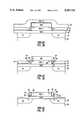
- FIG. 1shows a plan diagram that illustrates a representation of a virtual-ground EPROM or flash array 10.
- array 10includes a number of columns of buried bit lines BL1-BLn which alternately represent the drain and the source of the memory cells 14 of array 10.
- Array 10also includes a number of word lines WL1-WLn which orthogonally intersect each of the buried bit lines BL1-BLn.
- electrical contacts 18are formed on each end of the buried bit lines BL1-BLn. Thus, the electrical contacts form a bit line contact for every n cells.
- FIGS. 2A-2Hshow a cross-sectional diagram taken along lines 2A--2A of FIG. 1 that illustrates a process flow for the fabrication of the virtual ground, buried bit line array 10.
- the arrayis conventionally fabricated by first forming a layer of gate oxide 22 on a P-type silicon substrate 20. This is followed by the deposition of a layer of polysilicon (polyl) 24 and the formation of an overlying layer of oxide-nitride-oxide (ONO) 26. Next, an ONO/polyl mask is formed over the layer of ONO 26 and patterned to define rows of ONO/polyl strips 28. The unmasked layer of ONO 26 and the corresponding underlying layer of polyl 24 are then etched until the underlying layer of gate oxide 22 is exposed.
- polysiliconpolysilicon
- ONOoxide-nitride-oxide
- arsenicis implanted to define the N+ buried bit lines 30 of the virtual-ground array.
- the ONO/polyl maskis stripped, and a thin layer of edge oxide 32 is grown on each ONO/polyl strip 28 and the exposed layer of gate oxide 22 between the rows of ONO/polyl strips 28.
- substantially no edge oxide 32is grown on the layer of ONO 26 due to the lack of an oxidizing material.
- a layer of differential oxide 34is grown over the layer of edge oxide 32. As with the layer of edge oxide 32, substantially no differential oxide 34 is grown over the layer of ONO 26.
- oxide wedges 38are formed as a result of the oxidation of a portion of the layer of polyl 24 at the outer boundary between the layers of polyl 24 and ONO 26.
- the recesses 36 and the oxide wedges 38in turn cause the formation of poly2 remnants and polyl stringers, respectively.
- the poly2 remnantsmay cause word line to word line shorts while the polyl stringers may cause polyl floating gate to polyl floating gate shorts.
- the recesses 36define the minimum thickness of the layer of differential oxide 34 that is formed over the N+ buried bit lines 30.
- the recesses 36can cause portions of the N+ buried bit lines 30 to be trenched in subsequent etching steps.
- a second layer of polysilicon (poly2) 40is deposited on the layer of differential oxide 34. Once the layer of poly2 40 has been deposited, the word lines WL1-WLn of FIG. 1 are formed.
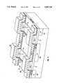
- FIG. 3shows a perspective view taken between lines 3A--3A and lines 3AA--3AA of FIG. 1 that illustrates the ideal formation of word lines WL1 and WL2.
- the word lines WL1 and WL2are ideally formed by removing the layers of poly2 40, ONO 26, and polyl 24 that have been formed in the regions 42 between the word lines WL1 and WL2.
- a poly2 mask(not shown) is formed on the array to define the word lines.
- the unmasked areas of the layer of poly2 40are anisotropically etched until the layers of differential oxide 34 and ONO 26 are exposed.
- the etching chemistries which are typically utilized to etch poly2have a high-selectivity with respect to differential oxide and ONO.
- the layers of differential oxide 34 and ONO 26remain substantially intact.
- poly2 remnants 44are formed in the recesses 36 because a portion 46 of the layer of differential oxide 34 effectively functions as a mask. As stated above and as shown in FIG. 4, the poly2 remnants 44 can cause shorts between adjacent poly2 word lines such as word lines WL1 and WL2.
- the layer of ONO 26 and the minimal layers of differential oxide 34 and edge oxide 32are etched with an etching chemistry which typically has a relatively high-selectivity between the remaining layer of poly and the layers of differential oxide 34, edge oxide 32, and ONO 26.
- the minimum thickness R of the combined layers of differential oxide 34 and edge oxide 32must be greater than the combined thickness T of the layer of ONO 26 and an oxide wedge 38.
- the principal disadvantage of failing to remove the oxide wedges 38is the formation of polyl stringers 48 which, as stated above, also can result in shorts between the polyl floating gates of adjacent memory cells 14.
- the layer of polylis removed with an anisotropic etch.
- the oxide wedges 38function as masks which prevent the polyl anisotropic etch from removing the polyl material which lies below the oxide wedges 38.
- the minimum thickness R of the combined layers of differential oxide 34 and edge oxide 32must be greater than the combined thickness T of the oxide wedges 38 and the layers of differential oxide 34, edge oxide 32 and ONO 26.
- the problems presented by oxide thinningcan be simply solved by merely insuring that the combined thickness R is greater than the combined thickness T.
- the problem with this approachis that the oxidation process which is utilized to form the layer of differential oxide 34 also diffuses the N+ buried bit lines 30, thereby reducing the channel length CL of the resulting memory cells.
- the differential oxide fabrication timeis extended to insure that the thickness R is greater than the thickness T, the channel lengths CL of the resulting memory cells are substantially reduced.
- the present inventionprovides a method of fabricating an electrically-programmable read-only-memory (EPROM) or a flash memory array that controls oxide thinning to prevent electrical shorts in the array and to prevent trenching of the bit lines.
- the methodbegins with the following steps. First, a layer of gate oxide is formed on a silicon substrate of P-type conductivity. This is followed by the formation of a layer of first polysilicon (polyl) on the layer of gate oxide. Next, a layer of oxide-nitride-oxide (ONO) is formed on the layer of polyl. Following this, a layer of second polysilicon (poly cap) is formed on the layer of ONO.
- EPROMelectrically-programmable read-only-memory
- ONOoxide-nitride-oxide
- a layer of nitrideis formed on the poly cap layer.
- a layer of third polysiliconis deposited on the layer of nitride.
- the thin poly/nitride/poly cap/ONO/polyl layersare then etched to define rows of parallel thin poly/nitride/poly cap/ONO/polyl strips which, in turn, inherently define parallel strips of gate oxide material therebetween.
- spacersare formed on the sidewalls of the parallel strips. The spacers are formed by forming a layer of edge oxide on the thin poly/nitride/poly cap/ONO/polyl strips and the exposed layer of gate oxide therebetween.
- a layer of spacer oxideis formed on the layer of edge oxide.
- the spacer oxidecan be, for example, a conformally deposited oxide such as low-pressure chemically-vapor-deposited oxide.
- the spacersare then formed by etching the layer of spacer oxide and the layer of edge oxide until both the substrate and the thin poly layer are exposed.
- An N-type dopantis then introduced into the parallel strips of substrate material to define the N+ buried bit lines of the EPROM or flash array.
- a thin layer of oxidecan be formed on the substrate material prior to the introduction of the dopant material. After the dopant is introduced, a layer of differential oxide is formed over the structure resulting from the above-listed steps. After this, the process continues with conventional steps.
- spacersaccording to the above described method provides a technique for eliminating the poly2 remnants and the polyl stringers as discussed above.
- the N+ bit line implantis formed after the formation of the spacers, adjoining bit lines are initially formed farther apart. This allows a thicker layer of differential oxide to be formed without reducing the size of the channel length due to N+ diffusion, and incidentally provides a means for controlling the size of the channel length.
- FIG. 1is a plan diagram illustrating a portion of a conventional virtual-ground EPROM or flash array 10.
- FIGS. 2A-2Hare a cross-sectional diagram taken along lines 2A--2A of FIG. 1 illustrating a process flow for the fabrication of the virtual ground, buried bit line array 10.
- FIG. 3is a perspective view taken between lines 3A--3A and 3AA--3AA of FIG. 1 illustrating the formation of the word lines WL1-WLn of FIG. 1.
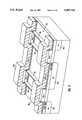
- FIG. 4is a perspective view of a portion of array 10 illustrating a word line-to-word line short resulting from remnant 44.
- FIG. 5is a perspective view of a portion of array 10 illustrating a floating gate-to-floating gate short between adjacent memory cells 14.
- FIGS. 6A-6Fare cross-sectional diagrams illustrating a process flow for fabricating a virtual ground, buried bit line EPROM or flash array that, in accordance with the concepts of the present invention, reduces the oxide thinning during the formation of the layer of differential oxide.
- FIG. 7is a cross-sectional diagram illustrating a first alternative embodiment of the present invention.
- FIGS. 6A-6Fshow a cross-sectional diagram that illustrates a process flow for fabricating a virtual ground, buried bit line EPROM or flash array that, in accordance with the concepts of the present invention, reduces the formation of the oxide wedges in the floating gate and eliminates the formation of the recesses in the layer of differential oxide.
- oxide wedgesthe likelihood of floating gate to floating gates shorts can be reduced.
- recessesthe problem of word line to word line shorts, as well as bit line trenching, can be eliminated.
- the processinitially begins by growing a layer of gate oxide 102 approximately 100-200 ⁇ thick on an underlying P-type substrate 100.
- a layer of polysilicon (polyl) 104which has been doped to an appropriate conductivity, is deposited on the layer of gate oxide 102, approximately 2000 ⁇ thick.
- a layer of oxide-nitride-oxide (ONO) 106approximately 250 ⁇ thick is formed on the layer of polyl 104.
- a second layer of polysilicon (poly cap) 108is deposited on the layer of ONO 106 with a thickness of approximately 1000 ⁇ .
- a layer of nitride 110approximately 100 ⁇ thick is formed on the poly cap 108 to prevent oxidation of the poly cap 108.
- a third layer of polysilicon (thin poly) 112approximately 100-200 ⁇ thick is deposited on the layer of nitride 110 to provide an etch stop during the subsequent etch of a layer of conformally deposited oxide.
- a poly1 mask(not shown) is formed on the thin poly layer 112 to define rows of parallel strips 114.
- the polyl maskis formed by utilizing conventional photoresist formation, photolithographic exposure, development and removal techniques. As shown in FIG. 6A, after the polyl mask has been formed, the rows of parallel strips 114 are formed by anisotropically etching the unmasked areas until the layer of gate oxide 102 is exposed.
- the polyl maskis stripped.
- a layer of edge oxide 116 approximately 200 ⁇ thickis grown by oxidizing both the rows of parallel strips 114 and the exposed layer of gate oxide 102 between the rows of parallel strips 114. Since, as stated above, the thin poly layer 112 is formed to provide a subsequent etch stop, the thin poly layer 112 must have a minimum thickness which insures that a functional etch stop will remain once the thin poly layer 112 has been partially oxidized during the formation of the layer of edge oxide 116. Further, as shown in FIG. 6B and as is well known in the art, substantially no edge oxide grows on the layer of nitride 110 or the layer of ONO 106.
- a layer of low-pressure chemically-vapor-deposited (LPCVD) oxide 118such as a silane-based oxide, is conformally deposited on the layer of edge oxide 116 with a thickness of about 1000 ⁇ .
- LPCVDlow-pressure chemically-vapor-deposited
- spacers 120are formed on the sidewalls 122 of each parallel strip 114. As shown in FIG. 6C, the spacers 120 are formed by anisotropically etching the layer of LPCVD oxide and the layer of edge oxide 116 until both the substrate 100 and the thin poly layer 112 are exposed. As shown in FIG. 6D, once the spacers 120 have been formed, arsenic or a similar dopant is implanted to define the N+ buried bit lines 126.
- a thin layer of edge oxide(not shown) can be formed on the substrate 100 and the thin poly layer 112 prior to implanting the dopant to define the N+ buried bit lines 126.
- the thin layer of edge oxide formed over the substrate 100acts to protect the substrate during the implant process.
- the resulting structureis oxidized to form a layer of differential oxide 128 on the parallel strips 114 and the substrate 110.
- the remaining portion of the thin poly layer 112is completely consumed during this oxidation step while a layer of differential oxide 128 approximately 800 ⁇ thick is formed on the substrate 100.
- substantially no differential oxidegrows on the spacers 120.
- the resulting structureis etched until the oxidized layer of thin poly and the layer of nitride 110 are removed. As a result of this etching step, the thickness of the layer of differential oxide 128 over the N+ buried bit lines 126 is also reduced.
- a second layer of polysilicon(not shown) is deposited.
- the second layer of polysiliconis then masked and etched to form the word line (not shown).
- the resulting polysilicon word lineis then used as a self-aligned mask to define the final structure.
- FIG. 6EThe advantages of the present invention are apparent from FIG. 6E.
- the structural stress that is present with the curved shape of the spacers 120 as well as the uniform growth of differential oxide on the substrate 100causes relatively minor recesses to be formed which are completely accessible by an anisotropic etch.
- the oxide wedgesas described above, can be substantially reduced in size.
- only minimal oxide wedgesare formed during the formation of the layer of edge oxide.
- the process of the present inventionalso provides control over the channel lengths of the resulting memory cells.
- FIG. 7shows a cross-sectional diagram that illustrates a first alternative embodiment of the present invention.
- a second layer of nitride (nit2) 134can be formed on the layer of thin poly 112. Following this, the process continues as described above.
- the nit2 layer 134is then removed at the same time the LPCVD oxide 118 and the edge oxide 116 are etched back to form the spacers 120.
- the advantage of the nit2 layer 134is that the nit2 layer 134 will prevent the partial oxidation of the thin poly layer 112 when the layer of edge oxide 116 is subsequently formed. By preventing the partial oxidation of the thin poly layer 112, an even thinner layer of thin poly 112 can be deposited to form the etch stop.
Landscapes
- Semiconductor Memories (AREA)
- Non-Volatile Memory (AREA)
Abstract
Description
Claims (9)
Priority Applications (5)
| Application Number | Priority Date | Filing Date | Title |
|---|---|---|---|
| US08/144,677US5397725A (en) | 1993-10-28 | 1993-10-28 | Method of controlling oxide thinning in an EPROM or flash memory array |
| EP94922626AEP0725979A1 (en) | 1993-10-28 | 1994-07-15 | Method of controlling oxide thinning in an eprom or flash memory array |
| KR1019960702170AKR960706191A (en) | 1993-10-28 | 1994-07-15 | METHOD OF CONTROLLING OXIDE THINNING IN AN EPROM OR FLASH MEMORY ARRAY |
| JP7504227AJPH09504410A (en) | 1993-10-28 | 1994-07-15 | Method for controlling thinning of oxide film in EPROM or flash memory array |
| PCT/US1994/008133WO1995012213A1 (en) | 1993-10-28 | 1994-07-15 | Method of controlling oxide thinning in an eprom or flash memory array |
Applications Claiming Priority (1)
| Application Number | Priority Date | Filing Date | Title |
|---|---|---|---|
| US08/144,677US5397725A (en) | 1993-10-28 | 1993-10-28 | Method of controlling oxide thinning in an EPROM or flash memory array |
Publications (1)
| Publication Number | Publication Date |
|---|---|
| US5397725Atrue US5397725A (en) | 1995-03-14 |
Family
ID=22509644
Family Applications (1)
| Application Number | Title | Priority Date | Filing Date |
|---|---|---|---|
| US08/144,677Expired - Fee RelatedUS5397725A (en) | 1993-10-28 | 1993-10-28 | Method of controlling oxide thinning in an EPROM or flash memory array |
Country Status (5)
| Country | Link |
|---|---|
| US (1) | US5397725A (en) |
| EP (1) | EP0725979A1 (en) |
| JP (1) | JPH09504410A (en) |
| KR (1) | KR960706191A (en) |
| WO (1) | WO1995012213A1 (en) |
Cited By (38)
| Publication number | Priority date | Publication date | Assignee | Title |
|---|---|---|---|---|
| US5672529A (en)* | 1994-03-31 | 1997-09-30 | Hitachi, Ltd. | Method of manufacturing nonvolatile semiconductor memory device |
| WO1997050120A1 (en)* | 1996-06-24 | 1997-12-31 | Macronix America, Inc. | Self-aligned isolation and planarization process for memory array |
| US5721448A (en)* | 1996-07-30 | 1998-02-24 | International Business Machines Corporation | Integrated circuit chip having isolation trenches composed of a dielectric layer with oxidation catalyst material |
| US5757059A (en)* | 1996-07-30 | 1998-05-26 | International Business Machines Corporation | Insulated gate field effect transistor |
| US5824580A (en)* | 1996-07-30 | 1998-10-20 | International Business Machines Corporation | Method of manufacturing an insulated gate field effect transistor |
| US5850091A (en)* | 1995-11-27 | 1998-12-15 | Sony Corporation | Semiconductor memory device and method of reading a data therefrom |
| US5917214A (en)* | 1997-01-06 | 1999-06-29 | Mosel Vitelic, Inc. | Split gate flash memory unit |
| US5923976A (en)* | 1995-12-26 | 1999-07-13 | Lg Semicon Co., Ltd. | Nonvolatile memory cell and method of fabricating the same |
| US5994239A (en)* | 1997-12-18 | 1999-11-30 | Advanced Micro Devices, Inc. | Manufacturing process to eliminate polystringers in high density nand-type flash memory devices |
| US6057193A (en)* | 1998-04-16 | 2000-05-02 | Advanced Micro Devices, Inc. | Elimination of poly cap for easy poly1 contact for NAND product |
| US6063668A (en)* | 1997-12-18 | 2000-05-16 | Advanced Micro Devices, Inc. | Poly I spacer manufacturing process to eliminate polystringers in high density nand-type flash memory devices |
| US6218227B1 (en)* | 1999-10-25 | 2001-04-17 | Advanced Micro Devices, Inc. | Method to generate a MONOS type flash cell using polycrystalline silicon as an ONO top layer |
| US6222241B1 (en)* | 1999-10-29 | 2001-04-24 | Advanced Micro Devices, Inc. | Method and system for reducing ARC layer removal by providing a capping layer for the ARC layer |
| US6281078B1 (en)* | 1997-12-18 | 2001-08-28 | Advanced Micro Devices, Inc. | Manufacturing process to eliminate ONO fence material in high density NAND-type flash memory devices |
| US20030235075A1 (en)* | 2002-06-21 | 2003-12-25 | Micron Technology, Inc. | Vertical NROM having a storage density of 1bit per 1F2 |
| US20040130934A1 (en)* | 2002-06-21 | 2004-07-08 | Micron Technology, Inc. | NROM memory cell, memory array, related devices and methods |
| US6830963B1 (en) | 2003-10-09 | 2004-12-14 | Micron Technology, Inc. | Fully depleted silicon-on-insulator CMOS logic |
| US20040265011A1 (en)* | 2003-06-30 | 2004-12-30 | Kiyonori Tsuda | Powder transport apparatus and image forming apparatus that can stabilize replenishment of powder |
| US20050001229A1 (en)* | 2003-07-01 | 2005-01-06 | Leonard Forbes | Apparatus and method for split transistor memory having improved endurance |
| US20050030794A1 (en)* | 2003-08-07 | 2005-02-10 | Micron Technology, Inc. | Method for erasing an NROM cell |
| US20050030792A1 (en)* | 2003-08-07 | 2005-02-10 | Micron Technology, Inc. | Method for programming and erasing an nrom cell |
| US20050051830A1 (en)* | 2003-09-05 | 2005-03-10 | Micron Technology, Inc. | Trench corner effect bidirectional flash memory cell |
| US6878991B1 (en) | 2004-01-30 | 2005-04-12 | Micron Technology, Inc. | Vertical device 4F2 EEPROM memory |
| US20050105341A1 (en)* | 2003-11-04 | 2005-05-19 | Micron Technology, Inc. | NROM flash memory with self-aligned structural charge separation |
| US20050106811A1 (en)* | 2003-11-17 | 2005-05-19 | Micron Technology, Inc. | NROM flash memory devices on ultrathin silicon |
| US20050128804A1 (en)* | 2003-12-16 | 2005-06-16 | Micron Technology, Inc. | Multi-state NROM device |
| US20050133860A1 (en)* | 2003-12-17 | 2005-06-23 | Micron Technology, Inc. | Vertical NROM NAND flash memory array |
| US20050138262A1 (en)* | 2003-12-18 | 2005-06-23 | Micron Technology, Inc. | Flash memory having a high-permittivity tunnel dielectric |
| US20050173755A1 (en)* | 2004-02-10 | 2005-08-11 | Micron Technology, Inc. | NROM flash memory with a high-permittivity gate dielectric |
| US20050174847A1 (en)* | 2004-02-10 | 2005-08-11 | Micron Technology, Inc. | Nrom flash memory cell with integrated dram |
| US20050184337A1 (en)* | 2004-02-24 | 2005-08-25 | Micron Technology, Inc. | 4f2 eeprom nrom memory arrays with vertical devices |
| US20050185466A1 (en)* | 2004-02-24 | 2005-08-25 | Micron Technology, Inc. | Multi-state memory cell with asymmetric charge trapping |
| US20050212033A1 (en)* | 2004-03-24 | 2005-09-29 | Micron Technology, Inc. | Memory device with high dielectric constant gate dielectrics and metal floating gates |
| US20050214994A1 (en)* | 2003-12-24 | 2005-09-29 | Kabushiki Kaisha Toshiba | Semiconductor device and method of fabricating the same |
| US20050247972A1 (en)* | 2004-05-06 | 2005-11-10 | Micron Technology, Inc. | Ballistic direct injection NROM cell on strained silicon structures |
| US6979857B2 (en) | 2003-07-01 | 2005-12-27 | Micron Technology, Inc. | Apparatus and method for split gate NROM memory |
| US20060124992A1 (en)* | 2003-12-16 | 2006-06-15 | Micron Technology, Inc. | NROM memory cell, memory array, related devices and methods |
| US20080067579A1 (en)* | 2006-09-18 | 2008-03-20 | Lee Joo-Hyeon | Flash memory device and method for manufacturing the same |
Citations (9)
| Publication number | Priority date | Publication date | Assignee | Title |
|---|---|---|---|---|
| GB2156586A (en)* | 1984-02-24 | 1985-10-09 | Hitachi Ltd | A semiconductor device with an insulated gate and an adjacent dense insulation layer |
| JPS6362382A (en)* | 1986-09-03 | 1988-03-18 | Nec Corp | Floating gate nonvolatile semiconductor storage device and manufacture thereof |
| US4749443A (en)* | 1986-12-04 | 1988-06-07 | Texas Instruments Incorporated | Sidewall oxide to reduce filaments |
| US5102814A (en)* | 1990-11-02 | 1992-04-07 | Intel Corporation | Method for improving device scalability of buried bit line flash EPROM devices having short reoxidation beaks and shallower junctions |
| US5149665A (en)* | 1991-07-10 | 1992-09-22 | Micron Technology, Inc. | Conductive source line for high density programmable read-only memory applications |
| US5151375A (en)* | 1990-06-13 | 1992-09-29 | Waferscale Integration, Inc. | EPROM virtual ground array |
| US5204835A (en)* | 1990-06-13 | 1993-04-20 | Waferscale Integration Inc. | Eprom virtual ground array |
| US5210047A (en)* | 1991-12-12 | 1993-05-11 | Woo Been Jon K | Process for fabricating a flash EPROM having reduced cell size |
| US5240870A (en)* | 1991-04-18 | 1993-08-31 | National Semiconductor Corporation | Stacked gate process flow for cross-point EPROM with internal access transistor |
- 1993
- 1993-10-28USUS08/144,677patent/US5397725A/ennot_activeExpired - Fee Related
- 1994
- 1994-07-15JPJP7504227Apatent/JPH09504410A/enactivePending
- 1994-07-15EPEP94922626Apatent/EP0725979A1/ennot_activeWithdrawn
- 1994-07-15KRKR1019960702170Apatent/KR960706191A/ennot_activeAbandoned
- 1994-07-15WOPCT/US1994/008133patent/WO1995012213A1/ennot_activeApplication Discontinuation
Patent Citations (9)
| Publication number | Priority date | Publication date | Assignee | Title |
|---|---|---|---|---|
| GB2156586A (en)* | 1984-02-24 | 1985-10-09 | Hitachi Ltd | A semiconductor device with an insulated gate and an adjacent dense insulation layer |
| JPS6362382A (en)* | 1986-09-03 | 1988-03-18 | Nec Corp | Floating gate nonvolatile semiconductor storage device and manufacture thereof |
| US4749443A (en)* | 1986-12-04 | 1988-06-07 | Texas Instruments Incorporated | Sidewall oxide to reduce filaments |
| US5151375A (en)* | 1990-06-13 | 1992-09-29 | Waferscale Integration, Inc. | EPROM virtual ground array |
| US5204835A (en)* | 1990-06-13 | 1993-04-20 | Waferscale Integration Inc. | Eprom virtual ground array |
| US5102814A (en)* | 1990-11-02 | 1992-04-07 | Intel Corporation | Method for improving device scalability of buried bit line flash EPROM devices having short reoxidation beaks and shallower junctions |
| US5240870A (en)* | 1991-04-18 | 1993-08-31 | National Semiconductor Corporation | Stacked gate process flow for cross-point EPROM with internal access transistor |
| US5149665A (en)* | 1991-07-10 | 1992-09-22 | Micron Technology, Inc. | Conductive source line for high density programmable read-only memory applications |
| US5210047A (en)* | 1991-12-12 | 1993-05-11 | Woo Been Jon K | Process for fabricating a flash EPROM having reduced cell size |
Non-Patent Citations (2)
| Title |
|---|
| B. Eitan, R. Kazerounian and A. Bergemont, "Alternate Metal Virtual Ground (AMG)--A New Scaling Concept for Very High-Density EPROM's," IEEE Electron Device Letters, Aug. 1991, vol. 12, No. 8, pp. 450-452. |
| B. Eitan, R. Kazerounian and A. Bergemont, Alternate Metal Virtual Ground (AMG) A New Scaling Concept for Very High Density EPROM s, IEEE Electron Device Letters, Aug. 1991, vol. 12, No. 8, pp. 450 452.* |
Cited By (165)
| Publication number | Priority date | Publication date | Assignee | Title |
|---|---|---|---|---|
| US6406958B2 (en)* | 1994-03-31 | 2002-06-18 | Hitachi, Ltd. | Method of manufacturing nonvolatile semiconductor memory device |
| US5932909A (en)* | 1994-03-31 | 1999-08-03 | Hitachi, Ltd. | Nonvolatile semiconductor memory device |
| US5672529A (en)* | 1994-03-31 | 1997-09-30 | Hitachi, Ltd. | Method of manufacturing nonvolatile semiconductor memory device |
| US5850091A (en)* | 1995-11-27 | 1998-12-15 | Sony Corporation | Semiconductor memory device and method of reading a data therefrom |
| US5923976A (en)* | 1995-12-26 | 1999-07-13 | Lg Semicon Co., Ltd. | Nonvolatile memory cell and method of fabricating the same |
| US5763309A (en)* | 1996-06-24 | 1998-06-09 | Macronix International Co., Ltd. | Self-aligned isolation and planarization process for memory array |
| WO1997050120A1 (en)* | 1996-06-24 | 1997-12-31 | Macronix America, Inc. | Self-aligned isolation and planarization process for memory array |
| US5824580A (en)* | 1996-07-30 | 1998-10-20 | International Business Machines Corporation | Method of manufacturing an insulated gate field effect transistor |
| US5757059A (en)* | 1996-07-30 | 1998-05-26 | International Business Machines Corporation | Insulated gate field effect transistor |
| US5721448A (en)* | 1996-07-30 | 1998-02-24 | International Business Machines Corporation | Integrated circuit chip having isolation trenches composed of a dielectric layer with oxidation catalyst material |
| US5917214A (en)* | 1997-01-06 | 1999-06-29 | Mosel Vitelic, Inc. | Split gate flash memory unit |
| US5994239A (en)* | 1997-12-18 | 1999-11-30 | Advanced Micro Devices, Inc. | Manufacturing process to eliminate polystringers in high density nand-type flash memory devices |
| US6063668A (en)* | 1997-12-18 | 2000-05-16 | Advanced Micro Devices, Inc. | Poly I spacer manufacturing process to eliminate polystringers in high density nand-type flash memory devices |
| US6281078B1 (en)* | 1997-12-18 | 2001-08-28 | Advanced Micro Devices, Inc. | Manufacturing process to eliminate ONO fence material in high density NAND-type flash memory devices |
| US6057193A (en)* | 1998-04-16 | 2000-05-02 | Advanced Micro Devices, Inc. | Elimination of poly cap for easy poly1 contact for NAND product |
| US6312991B1 (en) | 1998-04-16 | 2001-11-06 | Advanced Micro Devices Inc. | Elimination of poly cap easy poly 1 contact for NAND product |
| US6218227B1 (en)* | 1999-10-25 | 2001-04-17 | Advanced Micro Devices, Inc. | Method to generate a MONOS type flash cell using polycrystalline silicon as an ONO top layer |
| US6222241B1 (en)* | 1999-10-29 | 2001-04-24 | Advanced Micro Devices, Inc. | Method and system for reducing ARC layer removal by providing a capping layer for the ARC layer |
| US20040130934A1 (en)* | 2002-06-21 | 2004-07-08 | Micron Technology, Inc. | NROM memory cell, memory array, related devices and methods |
| US8441056B2 (en) | 2002-06-21 | 2013-05-14 | Micron Technology, Inc. | NROM memory cell, memory array, related devices and methods |
| US20090010075A9 (en)* | 2002-06-21 | 2009-01-08 | Micron Technologies, Inc. | NROM memory cell, memory array, related devices and methods |
| US20040202032A1 (en)* | 2002-06-21 | 2004-10-14 | Micron Technology, Inc. | Vertical NROM having a storage density of 1 bit per 1F2 |
| US20030235075A1 (en)* | 2002-06-21 | 2003-12-25 | Micron Technology, Inc. | Vertical NROM having a storage density of 1bit per 1F2 |
| US6906953B2 (en) | 2002-06-21 | 2005-06-14 | Micron Technology, Inc. | Vertical NROM having a storage density of 1 bit per 1F2 |
| US20040066672A1 (en)* | 2002-06-21 | 2004-04-08 | Micron Technology, Inc. | Vertical NROM having a storage density of 1 bit per IF2 |
| US6842370B2 (en) | 2002-06-21 | 2005-01-11 | Micron Technology, Inc. | Vertical NROM having a storage density of 1 bit per 1F2 |
| US6853587B2 (en) | 2002-06-21 | 2005-02-08 | Micron Technology, Inc. | Vertical NROM having a storage density of 1 bit per 1F2 |
| US20060124998A1 (en)* | 2002-06-21 | 2006-06-15 | Micron Technology, Inc. | NROM memory cell, memory array, related devices and methods |
| US7230848B2 (en) | 2002-06-21 | 2007-06-12 | Micron Technology, Inc. | Vertical NROM having a storage density of 1 bit per 1F2 |
| US7541242B2 (en) | 2002-06-21 | 2009-06-02 | Micron Technology, Inc. | NROM memory cell, memory array, related devices and methods |
| US20060126398A1 (en)* | 2002-06-21 | 2006-06-15 | Micron Technologies, Inc. | NROM memory cell, memory array, related devices and methods |
| US7220634B2 (en) | 2002-06-21 | 2007-05-22 | Micron Technology, Inc. | NROM memory cell, memory array, related devices and methods |
| US7535048B2 (en) | 2002-06-21 | 2009-05-19 | Micron Technology, Inc. | NROM memory cell, memory array, related devices and methods |
| US20090072303A9 (en)* | 2002-06-21 | 2009-03-19 | Micron Technology, Inc. | Nrom memory cell, memory array, related devices and methods |
| US20050255647A1 (en)* | 2002-06-21 | 2005-11-17 | Micron Technology, Inc. | Vertical NROM having a storage density of 1 bit per 1F2 |
| US20040265011A1 (en)* | 2003-06-30 | 2004-12-30 | Kiyonori Tsuda | Powder transport apparatus and image forming apparatus that can stabilize replenishment of powder |
| US20050001229A1 (en)* | 2003-07-01 | 2005-01-06 | Leonard Forbes | Apparatus and method for split transistor memory having improved endurance |
| US6979857B2 (en) | 2003-07-01 | 2005-12-27 | Micron Technology, Inc. | Apparatus and method for split gate NROM memory |
| US7719046B2 (en) | 2003-07-01 | 2010-05-18 | Micron Technology, Inc. | Apparatus and method for trench transistor memory having different gate dielectric thickness |
| US20060197143A1 (en)* | 2003-07-01 | 2006-09-07 | Micron Technology, Inc. | Apparatus and method for split transistor memory having improved endurance |
| US7095075B2 (en) | 2003-07-01 | 2006-08-22 | Micron Technology, Inc. | Apparatus and method for split transistor memory having improved endurance |
| US20050141278A1 (en)* | 2003-08-07 | 2005-06-30 | Micron Technology, Inc. | Method for programming and erasing an NROM cell |
| US20070070700A1 (en)* | 2003-08-07 | 2007-03-29 | Micron Technology, Inc. | Method for programming and erasing an NROM cell |
| US7088619B2 (en) | 2003-08-07 | 2006-08-08 | Micron Technology, Inc. | Method for programming and erasing an NROM cell |
| US7075832B2 (en) | 2003-08-07 | 2006-07-11 | Micron Technology, Inc. | Method for erasing an NROM cell |
| US7986555B2 (en) | 2003-08-07 | 2011-07-26 | Micron Technology, Inc. | Method for programming and erasing an NROM cell |
| US20050174855A1 (en)* | 2003-08-07 | 2005-08-11 | Micron Technology, Inc. | Method for erasing an NROM cell |
| US7085170B2 (en) | 2003-08-07 | 2006-08-01 | Micron Technology, Ind. | Method for erasing an NROM cell |
| US7075831B2 (en) | 2003-08-07 | 2006-07-11 | Micron Technology, Inc. | Method for erasing an NROM cell |
| US7227787B2 (en) | 2003-08-07 | 2007-06-05 | Micron Technology, Inc. | Method for erasing an NROM cell |
| US20100067307A1 (en)* | 2003-08-07 | 2010-03-18 | Micron Technology, Inc. | Method for programming and erasing an nrom cell |
| US7272045B2 (en) | 2003-08-07 | 2007-09-18 | Micron Technology, Inc. | Method for programming and erasing an NROM cell |
| US7639530B2 (en) | 2003-08-07 | 2009-12-29 | Micron Technology, Inc. | Method for programming and erasing an NROM cell |
| US7277321B2 (en) | 2003-08-07 | 2007-10-02 | Micron Technology, Inc. | Method for programming and erasing an NROM cell |
| US20060133152A1 (en)* | 2003-08-07 | 2006-06-22 | Micron Technology, Inc. | Method for programming and erasing an NROM cell |
| US20050030794A1 (en)* | 2003-08-07 | 2005-02-10 | Micron Technology, Inc. | Method for erasing an NROM cell |
| US20050030792A1 (en)* | 2003-08-07 | 2005-02-10 | Micron Technology, Inc. | Method for programming and erasing an nrom cell |
| US6873550B2 (en) | 2003-08-07 | 2005-03-29 | Micron Technology, Inc. | Method for programming and erasing an NROM cell |
| US20070064466A1 (en)* | 2003-08-07 | 2007-03-22 | Micron Technology, Inc. | Method for programming and erasing an NROM cell |
| US20050253186A1 (en)* | 2003-09-05 | 2005-11-17 | Micron Technology, Inc. | Trench corner effect bidirectional flash memory cell |
| US7283394B2 (en) | 2003-09-05 | 2007-10-16 | Micron Technology, Inc. | Trench corner effect bidirectional flash memory cell |
| US6977412B2 (en) | 2003-09-05 | 2005-12-20 | Micron Technology, Inc. | Trench corner effect bidirectional flash memory cell |
| US7161217B2 (en) | 2003-09-05 | 2007-01-09 | Micron Technology, Inc. | Trench corner effect bidirectional flash memory cell |
| US7285821B2 (en) | 2003-09-05 | 2007-10-23 | Micron Technology, Inc. | Trench corner effect bidirectional flash memory cell |
| US7329920B2 (en) | 2003-09-05 | 2008-02-12 | Micron Technology, Inc. | Trench corner effect bidirectional flash memory cell |
| US20050255638A1 (en)* | 2003-09-05 | 2005-11-17 | Micron Technology, Inc. | Trench corner effect bidirectional flash memory cell |
| US20050258480A1 (en)* | 2003-09-05 | 2005-11-24 | Micron Technology, Inc. | Trench corner effect bidirectional flash memory cell |
| US20050269625A1 (en)* | 2003-09-05 | 2005-12-08 | Micron Technology, Inc. | Trench corner effect bidirectional flash memory cell |
| US7535054B2 (en) | 2003-09-05 | 2009-05-19 | Micron Technology, Inc. | Trench corner effect bidirectional flash memory cell |
| US20050051830A1 (en)* | 2003-09-05 | 2005-03-10 | Micron Technology, Inc. | Trench corner effect bidirectional flash memory cell |
| US7973370B2 (en) | 2003-10-09 | 2011-07-05 | Micron Technology, Inc. | Fully depleted silicon-on-insulator CMOS logic |
| US20050077564A1 (en)* | 2003-10-09 | 2005-04-14 | Micron Technology, Inc. | Fully depleted silicon-on-insulator CMOS logic |
| US6830963B1 (en) | 2003-10-09 | 2004-12-14 | Micron Technology, Inc. | Fully depleted silicon-on-insulator CMOS logic |
| US20110204431A1 (en)* | 2003-10-09 | 2011-08-25 | Micron Technology, Inc. | Fully depleted silicon-on-insulator cmos logic |
| US8174081B2 (en) | 2003-10-09 | 2012-05-08 | Micron Technology, Inc. | Fully depleted silicon-on-insulator CMOS logic |
| US7078770B2 (en) | 2003-10-09 | 2006-07-18 | Micron Technology, Inc. | Fully depleted silicon-on-insulator CMOS logic |
| US20070109871A1 (en)* | 2003-11-04 | 2007-05-17 | Micron Technology, Inc. | NROM flash memory with self-aligned structural charge separation |
| US20050105341A1 (en)* | 2003-11-04 | 2005-05-19 | Micron Technology, Inc. | NROM flash memory with self-aligned structural charge separation |
| US7480186B2 (en) | 2003-11-04 | 2009-01-20 | Micron Technology, Inc. | NROM flash memory with self-aligned structural charge separation |
| US7184315B2 (en) | 2003-11-04 | 2007-02-27 | Micron Technology, Inc. | NROM flash memory with self-aligned structural charge separation |
| US20050280094A1 (en)* | 2003-11-17 | 2005-12-22 | Micron Technology, Inc. | NROM flash memory devices on ultrathin silicon |
| US8183625B2 (en) | 2003-11-17 | 2012-05-22 | Micron Technology, Inc. | NROM flash memory devices on ultrathin silicon |
| US7358562B2 (en) | 2003-11-17 | 2008-04-15 | Micron Technology, Inc. | NROM flash memory devices on ultrathin silicon |
| US20050106811A1 (en)* | 2003-11-17 | 2005-05-19 | Micron Technology, Inc. | NROM flash memory devices on ultrathin silicon |
| US7378316B2 (en) | 2003-11-17 | 2008-05-27 | Micron Technology, Inc. | Method for fabricating semiconductor vertical NROM memory cells |
| US7276762B2 (en) | 2003-11-17 | 2007-10-02 | Micron Technology, Inc. | NROM flash memory devices on ultrathin silicon |
| US7276413B2 (en) | 2003-11-17 | 2007-10-02 | Micron Technology, Inc. | NROM flash memory devices on ultrathin silicon |
| US20080203467A1 (en)* | 2003-11-17 | 2008-08-28 | Micron Technology, Inc. | Nrom flash memory devices on ultrathin silicon |
| US20110163321A1 (en)* | 2003-11-17 | 2011-07-07 | Micron Technology, Inc. | Nrom flash memory devices on ultrathin silicon |
| US20070166927A1 (en)* | 2003-11-17 | 2007-07-19 | Micron Technology, Inc. | Nrom flash memory devices on ultrathin silicon |
| US7244987B2 (en) | 2003-11-17 | 2007-07-17 | Micron Technology, Inc. | NROM flash memory devices on ultrathin silicon |
| US7915669B2 (en) | 2003-11-17 | 2011-03-29 | Micron Technology, Inc. | NROM flash memory devices on ultrathin silicon |
| US20100270610A1 (en)* | 2003-11-17 | 2010-10-28 | Micron Technology, Inc. | Nrom flash memory devices on ultrathin silicon |
| US7768058B2 (en) | 2003-11-17 | 2010-08-03 | Micron Technology, Inc. | NROM flash memory devices on ultrathin silicon |
| US20050280089A1 (en)* | 2003-11-17 | 2005-12-22 | Micron Technology, Inc. | NROM flash memory devices on ultrathin silicon |
| US7202523B2 (en) | 2003-11-17 | 2007-04-10 | Micron Technology, Inc. | NROM flash memory devices on ultrathin silicon |
| US20050282334A1 (en)* | 2003-11-17 | 2005-12-22 | Micron Technology, Inc. | NROM flash memory devices on ultrathin silicon |
| US20060128104A1 (en)* | 2003-12-16 | 2006-06-15 | Micron Technology, Inc. | NROM memory cell, memory array, related devices and methods |
| US7301804B2 (en) | 2003-12-16 | 2007-11-27 | Micro Technology, Inc. | NROM memory cell, memory array, related devices and methods |
| US20060152978A1 (en)* | 2003-12-16 | 2006-07-13 | Micron Technology, Inc. | Multi-state NROM device |
| US7050330B2 (en) | 2003-12-16 | 2006-05-23 | Micron Technology, Inc. | Multi-state NROM device |
| US7371642B2 (en) | 2003-12-16 | 2008-05-13 | Micron Technology, Inc. | Multi-state NROM device |
| US20060128103A1 (en)* | 2003-12-16 | 2006-06-15 | Micron Technology, Inc. | NROM memory cell, memory array, related devices and methods |
| US20050128804A1 (en)* | 2003-12-16 | 2005-06-16 | Micron Technology, Inc. | Multi-state NROM device |
| US7238599B2 (en) | 2003-12-16 | 2007-07-03 | Micron Technology, Inc. | Multi-state NROM device |
| US20060166443A1 (en)* | 2003-12-16 | 2006-07-27 | Micron Technology, Inc. | Multi-state NROM device |
| US20060124967A1 (en)* | 2003-12-16 | 2006-06-15 | Micron Technology, Inc. | NROM memory cell, memory array, related devices and methods |
| US20060124992A1 (en)* | 2003-12-16 | 2006-06-15 | Micron Technology, Inc. | NROM memory cell, memory array, related devices and methods |
| US7269071B2 (en) | 2003-12-16 | 2007-09-11 | Micron Technology, Inc. | NROM memory cell, memory array, related devices and methods |
| US7750389B2 (en) | 2003-12-16 | 2010-07-06 | Micron Technology, Inc. | NROM memory cell, memory array, related devices and methods |
| US7269072B2 (en) | 2003-12-16 | 2007-09-11 | Micron Technology, Inc. | NROM memory cell, memory array, related devices and methods |
| US7339239B2 (en) | 2003-12-17 | 2008-03-04 | Micron Technology, Inc. | Vertical NROM NAND flash memory array |
| US7241654B2 (en) | 2003-12-17 | 2007-07-10 | Micron Technology, Inc. | Vertical NROM NAND flash memory array |
| US20050133860A1 (en)* | 2003-12-17 | 2005-06-23 | Micron Technology, Inc. | Vertical NROM NAND flash memory array |
| US20060261404A1 (en)* | 2003-12-17 | 2006-11-23 | Micron Technology, Inc. | Vertical NROM NAND flash memory array |
| US7528037B2 (en) | 2003-12-18 | 2009-05-05 | Micron Technology, Inc. | Flash memory having a high-permittivity tunnel dielectric |
| US20090191676A1 (en)* | 2003-12-18 | 2009-07-30 | Micron Technology, Inc. | Flash memory having a high-permittivity tunnel dielectric |
| US20050138262A1 (en)* | 2003-12-18 | 2005-06-23 | Micron Technology, Inc. | Flash memory having a high-permittivity tunnel dielectric |
| US7157769B2 (en) | 2003-12-18 | 2007-01-02 | Micron Technology, Inc. | Flash memory having a high-permittivity tunnel dielectric |
| US20050277243A1 (en)* | 2003-12-18 | 2005-12-15 | Micron Technology, Inc. | Flash memory having a high-permittivity tunnel dielectric |
| US20100087057A1 (en)* | 2003-12-24 | 2010-04-08 | Kabushiki Kaisha Toshiba | Semiconductor device and method of fabricating the same |
| US20050214994A1 (en)* | 2003-12-24 | 2005-09-29 | Kabushiki Kaisha Toshiba | Semiconductor device and method of fabricating the same |
| US7679128B2 (en)* | 2003-12-24 | 2010-03-16 | Kabushiki Kaisha Toshiba | Semiconductor device and method of fabricating the same |
| US20050167743A1 (en)* | 2004-01-30 | 2005-08-04 | Micron Technology, Inc. | Vertical device 4F2 EEPROM memory |
| US6878991B1 (en) | 2004-01-30 | 2005-04-12 | Micron Technology, Inc. | Vertical device 4F2 EEPROM memory |
| US7332773B2 (en) | 2004-01-30 | 2008-02-19 | Micron Technology, Inc. | Vertical device 4F2 EEPROM memory |
| US20060261405A1 (en)* | 2004-01-30 | 2006-11-23 | Micron Technology, Inc. | Vertical device 4F² eeprom memory |
| US7157771B2 (en) | 2004-01-30 | 2007-01-02 | Micron Technology, Inc. | Vertical device 4F2 EEPROM memory |
| US20050240867A1 (en)* | 2004-02-10 | 2005-10-27 | Micron Technology, Inc. | NROM flash memory cell with integrated DRAM |
| US20050275011A1 (en)* | 2004-02-10 | 2005-12-15 | Micron Technology, Inc. | NROM flash memory with a high-permittivity gate dielectric |
| US7479428B2 (en) | 2004-02-10 | 2009-01-20 | Leonard Forbes | NROM flash memory with a high-permittivity gate dielectric |
| US7221018B2 (en) | 2004-02-10 | 2007-05-22 | Micron Technology, Inc. | NROM flash memory with a high-permittivity gate dielectric |
| US20060019453A1 (en)* | 2004-02-10 | 2006-01-26 | Micron Technology, Inc. | NROM flash memory with a high-permittivity gate dielectric |
| US7319613B2 (en) | 2004-02-10 | 2008-01-15 | Micron Technology, Inc. | NROM flash memory cell with integrated DRAM |
| US20050174847A1 (en)* | 2004-02-10 | 2005-08-11 | Micron Technology, Inc. | Nrom flash memory cell with integrated dram |
| US7072213B2 (en) | 2004-02-10 | 2006-07-04 | Micron Technology, Inc. | NROM flash memory cell with integrated DRAM |
| US20050173755A1 (en)* | 2004-02-10 | 2005-08-11 | Micron Technology, Inc. | NROM flash memory with a high-permittivity gate dielectric |
| US6952366B2 (en) | 2004-02-10 | 2005-10-04 | Micron Technology, Inc. | NROM flash memory cell with integrated DRAM |
| US20060203555A1 (en)* | 2004-02-24 | 2006-09-14 | Micron Technology, Inc. | Multi-state memory cell with asymmetric charge trapping |
| US7577027B2 (en) | 2004-02-24 | 2009-08-18 | Micron Technology, Inc. | Multi-state memory cell with asymmetric charge trapping |
| US20050185466A1 (en)* | 2004-02-24 | 2005-08-25 | Micron Technology, Inc. | Multi-state memory cell with asymmetric charge trapping |
| US7616482B2 (en) | 2004-02-24 | 2009-11-10 | Micron Technology, Inc. | Multi-state memory cell with asymmetric charge trapping |
| US7072217B2 (en) | 2004-02-24 | 2006-07-04 | Micron Technology, Inc. | Multi-state memory cell with asymmetric charge trapping |
| US7911837B2 (en) | 2004-02-24 | 2011-03-22 | Micron Technology, Inc. | Multi-state memory cell with asymmetric charge trapping |
| US20060203554A1 (en)* | 2004-02-24 | 2006-09-14 | Micron Technology, Inc. | Multi-state memory cell with asymmetric charge trapping |
| US20100039869A1 (en)* | 2004-02-24 | 2010-02-18 | Micron Technology, Inc. | Multi-state memory cell with asymmetric charge trapping |
| US7075146B2 (en) | 2004-02-24 | 2006-07-11 | Micron Technology, Inc. | 4F2 EEPROM NROM memory arrays with vertical devices |
| US20050184337A1 (en)* | 2004-02-24 | 2005-08-25 | Micron Technology, Inc. | 4f2 eeprom nrom memory arrays with vertical devices |
| US7282762B2 (en) | 2004-02-24 | 2007-10-16 | Micron Technology, Inc. | 4F2 EEPROM NROM memory arrays with vertical devices |
| US7102191B2 (en) | 2004-03-24 | 2006-09-05 | Micron Technologies, Inc. | Memory device with high dielectric constant gate dielectrics and metal floating gates |
| US20050212033A1 (en)* | 2004-03-24 | 2005-09-29 | Micron Technology, Inc. | Memory device with high dielectric constant gate dielectrics and metal floating gates |
| US20050280048A1 (en)* | 2004-03-24 | 2005-12-22 | Micron Technology, Inc. | Memory device with high dielectric constant gate dielectrics and metal floating gates |
| US7268031B2 (en) | 2004-03-24 | 2007-09-11 | Micron Technology, Inc. | Memory device with high dielectric constant gate dielectrics and metal floating gates |
| US20060237775A1 (en)* | 2004-03-24 | 2006-10-26 | Micron Technology, Inc. | Memory device with high dielectric constant gate dielectrics and metal floating gates |
| US8076714B2 (en) | 2004-03-24 | 2011-12-13 | Micron Technology, Inc. | Memory device with high dielectric constant gate dielectrics and metal floating gates |
| US20090294830A1 (en)* | 2004-03-24 | 2009-12-03 | Micron Technology, Inc. | Memory device with high dielectric constant gate dielectrics and metal floating gates |
| US7550339B2 (en) | 2004-03-24 | 2009-06-23 | Micron Technology, Inc. | Memory device with high dielectric constant gate dielectrics and metal floating gates |
| US7586144B2 (en) | 2004-03-24 | 2009-09-08 | Micron Technology, Inc. | Memory device with high dielectric constant gate dielectrics and metal floating gates |
| US20050247972A1 (en)* | 2004-05-06 | 2005-11-10 | Micron Technology, Inc. | Ballistic direct injection NROM cell on strained silicon structures |
| US20060214220A1 (en)* | 2004-05-06 | 2006-09-28 | Micron Technology, Inc. | Ballistic direct injection NROM cell on strained silicon structures |
| US7859046B2 (en) | 2004-05-06 | 2010-12-28 | Micron Technology, Inc. | Ballistic direct injection NROM cell on strained silicon structures |
| US7683424B2 (en) | 2004-05-06 | 2010-03-23 | Micron Technology, Inc. | Ballistic direct injection NROM cell on strained silicon structures |
| US7274068B2 (en) | 2004-05-06 | 2007-09-25 | Micron Technology, Inc. | Ballistic direct injection NROM cell on strained silicon structures |
| US7618862B2 (en)* | 2006-09-18 | 2009-11-17 | Dongbu Hitek Co., Ltd. | Flash memory device and method for manufacturing the same |
| US20080067579A1 (en)* | 2006-09-18 | 2008-03-20 | Lee Joo-Hyeon | Flash memory device and method for manufacturing the same |
Also Published As
| Publication number | Publication date |
|---|---|
| KR960706191A (en) | 1996-11-08 |
| JPH09504410A (en) | 1997-04-28 |
| EP0725979A1 (en) | 1996-08-14 |
| WO1995012213A1 (en) | 1995-05-04 |
Similar Documents
| Publication | Publication Date | Title |
|---|---|---|
| US5397725A (en) | Method of controlling oxide thinning in an EPROM or flash memory array | |
| KR100231964B1 (en) | How to form a nonvolatile memory cell using polycrystalline silicon spacer tunnel regions | |
| US6346725B1 (en) | Contact-less array of fully self-aligned, triple polysilicon, source-side injection, nonvolatile memory cells with metal-overlaid wordlines | |
| US20060216891A1 (en) | Non-volatile memory device and method of fabricating the same | |
| US7410871B2 (en) | Split gate type flash memory device and method for manufacturing same | |
| US6479346B1 (en) | Semiconductor memory device and fabrication method thereof | |
| US6590253B2 (en) | Memory cell with self-aligned floating gate and separate select gate, and fabrication process | |
| US6177315B1 (en) | Method of fabricating a high density EEPROM array | |
| US5246874A (en) | Method of making fast access AMG EPROM | |
| JPH09321255A (en) | Method of manufacturing nonvolatile semiconductor memory device | |
| KR100199381B1 (en) | Flash Ipyrom Cell Manufacturing Method | |
| KR100363840B1 (en) | A Method of manufacturing a flash memory device | |
| US5576232A (en) | Fabrication process for flash memory in which channel lengths are controlled | |
| US7414282B2 (en) | Method of manufacturing a non-volatile memory device | |
| US7060627B2 (en) | Method of decreasing charging effects in oxide-nitride-oxide (ONO) memory arrays | |
| US5998262A (en) | Method for manufacturing ETOX cell having damage-free source region | |
| US6194271B1 (en) | Method for fabricating flash memory | |
| US20050045939A1 (en) | Split-gate memory cell, memory array incorporating same, and method of manufacture thereof | |
| KR950011030B1 (en) | Making method eeprom | |
| KR19990060607A (en) | Nonvolatile Memory Device and Manufacturing Method Thereof | |
| US20050179080A1 (en) | Method and system for forming source regions in memory devices | |
| KR100226771B1 (en) | Flash memory manufacturing method | |
| KR0183792B1 (en) | Nonvolatile Memory Device and Manufacturing Method | |
| KR100211072B1 (en) | Manufacture of semiconductor device | |
| KR0161393B1 (en) | Manufacturing method of nonvolatile semiconductor memory device |
Legal Events
| Date | Code | Title | Description |
|---|---|---|---|
| AS | Assignment | Owner name:NATIONAL SEMICONDUCTOR CORPORATION, CALIFORNIA Free format text:ASSIGNMENT OF ASSIGNORS INTEREST;ASSIGNOR:WOLSTENHOLME, GRAHAM RICHARD;REEL/FRAME:006825/0720 Effective date:19931101 Owner name:NATIONAL SEMICONDUCTOR CORPORATION, CALIFORNIA Free format text:ASSIGNMENT OF ASSIGNORS INTEREST;ASSIGNOR:BERGEMONT ALBERT;REEL/FRAME:006825/0718 Effective date:19931118 | |
| AS | Assignment | Owner name:BANKERS TRUST COMPANY, NEW YORK Free format text:SECURITY INTEREST;ASSIGNOR:FAIRCHILD SEMICONDUCTOR CORPORATION;REEL/FRAME:008454/0101 Effective date:19970311 Owner name:FAIRCHILD SEMICONDUCTOR CORPORATION, MAINE Free format text:ASSIGNMENT OF ASSIGNORS INTEREST;ASSIGNOR:NATIONAL SEMICONDUCTOR CORPORATION;REEL/FRAME:008535/0103 Effective date:19970311 | |
| FEPP | Fee payment procedure | Free format text:PAYOR NUMBER ASSIGNED (ORIGINAL EVENT CODE: ASPN); ENTITY STATUS OF PATENT OWNER: LARGE ENTITY | |
| REMI | Maintenance fee reminder mailed | ||
| FPAY | Fee payment | Year of fee payment:4 | |
| SULP | Surcharge for late payment | ||
| AS | Assignment | Owner name:CREDIT SUISSE FIRST BOSTON, NEW YORK Free format text:SECURITY AGREEMENT;ASSIGNOR:FAIRCHILD SEMICONDUCTOR CORPORATION;REEL/FRAME:009883/0800 Effective date:19990414 | |
| AS | Assignment | Owner name:FAIRCHILD SEMICONDUCTOR CORPORATION, MAINE Free format text:RELEASE BY SECURED PARTY;ASSIGNOR:BANKERS TRUST COMPANY;REEL/FRAME:009901/0528 Effective date:19990414 | |
| AS | Assignment | Owner name:FAIRCHILD SEMICONDUCTOR CORPORATION, MAINE Free format text:RELEASE;ASSIGNOR:CREDIT SUISSE FIRST BOSTON;REEL/FRAME:010996/0537 Effective date:20000602 | |
| LAPS | Lapse for failure to pay maintenance fees | ||
| LAPS | Lapse for failure to pay maintenance fees | Free format text:PATENT EXPIRED FOR FAILURE TO PAY MAINTENANCE FEES (ORIGINAL EVENT CODE: EXP.); ENTITY STATUS OF PATENT OWNER: LARGE ENTITY | |
| STCH | Information on status: patent discontinuation | Free format text:PATENT EXPIRED DUE TO NONPAYMENT OF MAINTENANCE FEES UNDER 37 CFR 1.362 | |
| FP | Lapsed due to failure to pay maintenance fee | Effective date:20030314 |