US5397432A - Method for producing semiconductor integrated circuits and apparatus used in such method - Google Patents
Method for producing semiconductor integrated circuits and apparatus used in such methodDownload PDFInfo
- Publication number
- US5397432A US5397432AUS07/743,383US74338391AUS5397432AUS 5397432 AUS5397432 AUS 5397432AUS 74338391 AUS74338391 AUS 74338391AUS 5397432 AUS5397432 AUS 5397432A
- Authority
- US
- United States
- Prior art keywords
- metallic film
- mask
- substrate
- plasma
- ashing
- Prior art date
- Legal status (The legal status is an assumption and is not a legal conclusion. Google has not performed a legal analysis and makes no representation as to the accuracy of the status listed.)
- Expired - Lifetime
Links
Images


Classifications
- H—ELECTRICITY
- H01—ELECTRIC ELEMENTS
- H01L—SEMICONDUCTOR DEVICES NOT COVERED BY CLASS H10
- H01L21/00—Processes or apparatus adapted for the manufacture or treatment of semiconductor or solid state devices or of parts thereof
- H01L21/02—Manufacture or treatment of semiconductor devices or of parts thereof
- H01L21/02041—Cleaning
- H01L21/02057—Cleaning during device manufacture
- H01L21/02068—Cleaning during device manufacture during, before or after processing of conductive layers, e.g. polysilicon or amorphous silicon layers
- H01L21/02071—Cleaning during device manufacture during, before or after processing of conductive layers, e.g. polysilicon or amorphous silicon layers the processing being a delineation, e.g. RIE, of conductive layers
- H—ELECTRICITY
- H01—ELECTRIC ELEMENTS
- H01L—SEMICONDUCTOR DEVICES NOT COVERED BY CLASS H10
- H01L21/00—Processes or apparatus adapted for the manufacture or treatment of semiconductor or solid state devices or of parts thereof
- H01L21/02—Manufacture or treatment of semiconductor devices or of parts thereof
- H01L21/04—Manufacture or treatment of semiconductor devices or of parts thereof the devices having potential barriers, e.g. a PN junction, depletion layer or carrier concentration layer
- H01L21/18—Manufacture or treatment of semiconductor devices or of parts thereof the devices having potential barriers, e.g. a PN junction, depletion layer or carrier concentration layer the devices having semiconductor bodies comprising elements of Group IV of the Periodic Table or AIIIBV compounds with or without impurities, e.g. doping materials
- H01L21/30—Treatment of semiconductor bodies using processes or apparatus not provided for in groups H01L21/20 - H01L21/26
- H01L21/31—Treatment of semiconductor bodies using processes or apparatus not provided for in groups H01L21/20 - H01L21/26 to form insulating layers thereon, e.g. for masking or by using photolithographic techniques; After treatment of these layers; Selection of materials for these layers
- H01L21/3105—After-treatment
- H01L21/311—Etching the insulating layers by chemical or physical means
- H01L21/31127—Etching organic layers
- H01L21/31133—Etching organic layers by chemical means
- H01L21/31138—Etching organic layers by chemical means by dry-etching
- H—ELECTRICITY
- H01—ELECTRIC ELEMENTS
- H01L—SEMICONDUCTOR DEVICES NOT COVERED BY CLASS H10
- H01L21/00—Processes or apparatus adapted for the manufacture or treatment of semiconductor or solid state devices or of parts thereof
- H01L21/02—Manufacture or treatment of semiconductor devices or of parts thereof
- H01L21/04—Manufacture or treatment of semiconductor devices or of parts thereof the devices having potential barriers, e.g. a PN junction, depletion layer or carrier concentration layer
- H01L21/18—Manufacture or treatment of semiconductor devices or of parts thereof the devices having potential barriers, e.g. a PN junction, depletion layer or carrier concentration layer the devices having semiconductor bodies comprising elements of Group IV of the Periodic Table or AIIIBV compounds with or without impurities, e.g. doping materials
- H01L21/30—Treatment of semiconductor bodies using processes or apparatus not provided for in groups H01L21/20 - H01L21/26
- H01L21/31—Treatment of semiconductor bodies using processes or apparatus not provided for in groups H01L21/20 - H01L21/26 to form insulating layers thereon, e.g. for masking or by using photolithographic techniques; After treatment of these layers; Selection of materials for these layers
- H01L21/3205—Deposition of non-insulating-, e.g. conductive- or resistive-, layers on insulating layers; After-treatment of these layers
- H01L21/321—After treatment
- H01L21/3213—Physical or chemical etching of the layers, e.g. to produce a patterned layer from a pre-deposited extensive layer
- H01L21/32133—Physical or chemical etching of the layers, e.g. to produce a patterned layer from a pre-deposited extensive layer by chemical means only
- H01L21/32135—Physical or chemical etching of the layers, e.g. to produce a patterned layer from a pre-deposited extensive layer by chemical means only by vapour etching only
- H01L21/32136—Physical or chemical etching of the layers, e.g. to produce a patterned layer from a pre-deposited extensive layer by chemical means only by vapour etching only using plasmas
- H—ELECTRICITY
- H01—ELECTRIC ELEMENTS
- H01L—SEMICONDUCTOR DEVICES NOT COVERED BY CLASS H10
- H01L21/00—Processes or apparatus adapted for the manufacture or treatment of semiconductor or solid state devices or of parts thereof
- H01L21/67—Apparatus specially adapted for handling semiconductor or electric solid state devices during manufacture or treatment thereof; Apparatus specially adapted for handling wafers during manufacture or treatment of semiconductor or electric solid state devices or components ; Apparatus not specifically provided for elsewhere
- H01L21/67005—Apparatus not specifically provided for elsewhere
- H01L21/67011—Apparatus for manufacture or treatment
- H01L21/67155—Apparatus for manufacturing or treating in a plurality of work-stations
- H01L21/67161—Apparatus for manufacturing or treating in a plurality of work-stations characterized by the layout of the process chambers
- H01L21/67173—Apparatus for manufacturing or treating in a plurality of work-stations characterized by the layout of the process chambers in-line arrangement
Definitions
- the present inventionrelates to a lithography process for use during the production of semiconductor integrated circuits. More particularly, it relates to the removal of chlorine or bromine which remains on a surface of a conductive film when the conductive film made of aluminum or an alloy thereof is dry-etched by using chlorine or bromine, or an alloy thereof as an etchant.
- a wiring forming a semiconductor integrated circuit formed on a substratesuch as silicon wafer or the like
- thin films of aluminum (Al) or thin films of an alloy in which silicon (Si) or copper (Co) is added into aluminumare often used.
- a so-called barrier metal of a thin film of titanium (Ti), titanium nitride (TiN), or titanium-tungsten (TiW)is provided between the silicon wafer and the aluminum thin film.
- Patterning of an aluminum or aluminum alloy film for such wiring as described aboveis performed generally by a lithography in which the conductive film is selectively etched by using a mask formed of a resist layer. Anisotropic etching is required to make it possible to form fine wiring patterns. At the present time, reactive ion etching (RIE) is a typical anisotropic etching method. For removing a resist mask, a so-called ashing, which can be performed Without using a solvent, such as trichloro ethylene which poses a problem relating to the environmental pollution, is used.
- RIEreactive ion etching
- etching and ashing methodsare both a dry process. So, they are suitable for process control or automatic processing and free from the contamination due to impurities in an etching solution or a solvent as in a wet process. An outline of these processes will now be explained with reference to FIGS. 1 and 2.
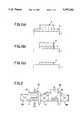
- FIGS. 1(a), 1(b), and 1(c)show a change in the cross section of a member to be processed in the above-described dry etching and ashing processes.
- FIG. 2schematically shows an example of the construction of a processing system for automatically performing the etching and ashing operations.
- a RIE apparatus 10 for etching aluminum films and an ashing apparatus 20 for removing resist masks after etchingare connected to each other via a load lock chamber 13 which is capable of a vacuum.
- Aluminum filmsare transported by the load lock chamber 13 from the RIE apparatus 10 to the ashing apparatus 20 without contacting the atmosphere.
- Another load lock chamber 13Ais disposed on the entry side of the RIE apparatus 10, and another load lock chamber 13B is disposed on the exit side of the ashing apparatus 20.
- Substrates on which aluminum films are formedcan be inserted into or taken out of the RIE apparatus 10 and the ashing apparatus 20 without introducing air into the apparatuses 10 and 20 by the load lock chambers 13A and 13B.
- an aluminum film 2is deposited on the whole of a surface of a substrate 1 composed of a silicon wafer, following which a resist is applied onto the aluminum film 2.
- a resistis applied onto the aluminum film 2.
- the surface of the substrate 1 on which the aluminum film 2 is formedis generally covered with an unillustrated insulation layer composed of SiO 2 , etc.
- the surface of the substrate 1 or a lower layer wiringis exposed inside a contact hole provided on a part of the insulation layer.
- the substrate 1 with the mask 3 formed thereon as described aboveis placed on a stage 11 inside the RIE apparatus 10 through the load lock chamber 13A in FIG. 2. Then, for example, chlorine gas (Cl 2 ) is introduced into the RIE apparatus 10 and, while the inside of such apparatus is being maintained at a predetermined pressure, a plasma is generated by applying a voltage between the stage 11 and an electrode 12. As a result, the aluminum film 2 is anisotropically etched, as shown in FIG. 1(b).
- the substrate 1 having the aluminum film 2 etched as described aboveis transported to the ashing apparatus 20 through the load lock chamber 13 in FIG. 2. Then, for example, an oxygen gas (O 2 ) is introduced into the ashing apparatus 20, and while the inside of such apparatus is being maintained at a predetermined pressure, a voltage is applied between a pair of electrodes 16 which are opposed to each other. As a result, a plasma is generated between the electrodes 16.
- the mask 3 composed of the aforesaid resistreacts mainly with oxygen atoms or molecules, or ions in this plasma and vaporizes, being exhausted outside the ashing apparatus 20. In this manner, the mask 3 on the aluminum film 2 is removed, as shown in FIG. 1(c).
- FIG. 2Shown in FIG. 2 is the ashing apparatus 20 which performs plasma ashing in which a member to be processed is directly exposed to the plasma.
- the above-described processesare performed in the same manner as for an automatic processing system equipped with a so-called down-flow type ashing apparatus which exposes the member to be processed to only neutral active species extracted from a plasma.
- excitation by microwave radiation or excitation using a high-frequency induction coilis often used in place of the electrode 16.
- gaseous chlorine compoundssuch as boron trichloride (BCl 3 ) or silicon tetrachloride (SiCl 4 ), bromine gas (Br 2 ), or gaseous bromine compounds, such as hydrogen bromide (HBr) or boron tribromine (BBr 3 ), are also used as an etchant.
- after-corrosionis due to the fact that chlorine, bromine, or their compounds, which are components of the etchant used in etching can, remain on the surface of an aluminum film. That is, the residual chlorine, for example, reacts with the water of the atmosphere, generating hydrochloric acid (HCl), etc., which causes aluminum films to become corroded.
- HClhydrochloric acid
- the introduction of the automatic processing system shown in FIG. 2enables an aluminum film to be sent to an ashing apparatus without being exposed to the atmosphere. And, since most of the remaining chlorine or the like are removed by the ashing apparatus. Accordingly, after-corrosion described above is considerably reduced.
- Al-Cu alloysin which electro-migration and stress migration do not often occur in comparison with pure aluminum films, have come to be used as a wiring material.
- thin films of Ti, TiN, or TiWare used as barrier metals for blocking the alloy reaction between a silicon substrate or polycrystal silicon lower-layer wiring, and aluminum wiring.
- Al-Cu alloy films or barrier metalspromotes after-corrosion because an electric cell is formed on the grain boundaries of different types of metals or the interface of the barrier metal and aluminum films because of the presence of hydrochloric acid generated from the above-mentioned residual chlorine. Therefore, even if the automatic processing system shown in FIG. 2 is introduced, a problem is posed in that after-corrosion cannot be completely avoided.
- the present inventionimproves the production yield of semiconductor integrated circuits having wiring composed of thin films of aluminum or an alloy thereof, and enhances the reliability of the semiconductor integrated circuits for use for a long period of time.
- the present inventionis characterized by including any one of the following modes. That is,
- a film 2 of aluminum or an alloy thereof formed on a surface of a substrate 1is covered with a mask 3 composed of a resist.
- the aluminum film 2is exposed through the mask 3 and selectively etched by using chlorine, bromine, or a gaseous etchant containing a compound thereof.
- the mask 3, used in the aforesaid etchingis ashed and removed, when it is directly exposed to a plasma generated in an atmosphere containing oxygen and water vapor, or exposed to neutral active species extracted from the plasma. Residual chlorine, bromine, or a compound thereof on the surface of the film 2 which is exposed as a result of the removal of the mask 3 is dissociated from the surface by forming volatile compounds, such as HCl, and removed.
- volatile compoundssuch as HCl
- the thin film 2is exposed directly to a plasma generated in an atmosphere containing water vapor or to neutral active species extracted from the plasma in order that residual chlorine or the like on the surface thereof is removed as described in above (1).
- O 2 and H 2 Oare shown as representative of the aforesaid neutral active species, CO 2 as representatives of the reaction products when the resist mask 3 is removed, and HCl as representative of the product when the aforesaid neutral active species and the residual chlorine react and are removed.
- the aforesaid neutral active species and the productsare not limited to these examples.
- An automatic processing systemis constructed in order that the removal of residual chlorine or the like in the mode (3) above, can be performed by using an apparatus different from an ashing apparatus. That is, as shown in FIG. 4, a after-treatment apparatus 40 is connected, via a load lock chamber 13C, to the ashing apparatus 20, which is connected to the RIE apparatus 10 via the load lock chamber 13.
- a down flow type or a plasma processing typewhere a member to be processed is directly exposed to the plasma, is used in the same manner as in the ashing apparatus 20.
- reference numeral 1denotes a substrate having a thin film of aluminum or an alloy thereof selectively covered with a resist mask but not etched.
- Reference numeral 1'denotes a substrate on which the aforesaid thin film is etched.
- Reference numeral 1"denotes a substrate from which the aforesaid resist mask has been removed.
- the applicant of the present inventionhas proposed an ashing method whereby water is added into the aforesaid gas for the purpose of increasing the ashing speed in down-stream ashing in which gases having oxygen are used (Japanese Patent Laid-Open No. 64-48421, Application date: Aug. 19, 1987).
- this methodhowever, conditions for etching (a process anterior to an ashing operation) are not specified.
- an etchantsuch as chlorine gas or the like.
- the applicant of the present inventionhas also proposed a method of preventing after-corrosion by exposing aluminum films which are etched by using a chlorine-type reactive gas, to water vapor in a pressure-reduced atmosphere (Japanese Patent Laid-Open No. 3-41728, Application date: Jul. 7, 1989).
- Japanese Patent Laid-Open No. 3-41728Application date: Jul. 7, 1989.
- the removal of residual components, such as chlorine or the like, which cause after-corrosiondepends on a thermal reaction, and a substrate to be processed is heated to approximately 120° C. in order to promote this reaction.
- aluminum films patterned by using an etchantsuch as chlorine gas or the like are exposed directly to a plasma generated in an atmosphere containing water vapor or to active species extracted from this plasma, such as H 2 O in an excited state or hydrogen (H) in an atomic state, or OH free radicals, or the like, in order for residual chlorine or the like to be removed.
- active species extracted from this plasmasuch as H 2 O in an excited state or hydrogen (H) in an atomic state, or OH free radicals, or the like
- FIG. 1is a schematic cross-sectional view showing a process for patterning wiring of a semiconductor integrated circuit
- FIG. 2is a schematic view showing an example of the construction of an automatic processing apparatus for performing wiring patterning in a semiconductor integrate circuit
- FIG. 3is a schematic cross-sectional view showing a principle of the present invention.
- FIG. 4is a schematic view showing an example of the construction of an automatic processing apparatus of the present invention.
- FIG. 5(a)is a schematic view showing an example of the construction of an automatic processing apparatus used for effecting the present invention
- FIG. 5(b)is a schematic view showing a detailed construction of an ashing apparatus 20 or an after-treatment apparatus 40 in FIG. 4 or FIG. 5(a);
- FIG. 6is a schematic sectional view showing an example of wiring construction processed by a method of the present invention.
- FIG. 7is a schematic view showing a detailed construction of an example of the substitute ashing apparatus 20 or the after-treatment apparatus 40 in FIG. 4 or FIG. 5(a);
- FIG. 8is a schematic view showing a detailed construction of an example of the substitute ashing apparatus 20 in FIG. 4 or FIG. 5(a);
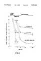
- FIG. 9is a graph showing an effect of reducing the amount of residual chlorine according to the present invention.
- a gaseous mixture of chlorine gas (Cl 2 ) and silicon tetrachloride (SiCl 4 )is introduced thereto.
- the total pressureis maintained at 8 ⁇ 10 -2 Torr, and a high-frequency voltage is applied between the stage 11 and the electrode 12.
- the aluminum film 2 (not shown) on the substrate 1is anisotropically etched by ions and radicals in the plasma generated between the stage 11 and the electrode 12.
- the substrate 1 with the aluminum film 2 etched as described aboveis transported to the ashing apparatus 20 through the load lock chamber 13 which has been turned into a vacuum and placed on a stage 14.
- the ashing apparatus 20 in the figureis of a so-called plasma ashing type.
- Oxygen gas (O 2 ) and water vapor (H 2 O)are introduced into the ashing apparatus 20 each at a flow rate of 1 to 2 SLM, and 100 to 300 SCCM, and the total pressure is maintained at 1 Torr.
- the substrate 1is heated, for example, to 100° to 200° C., by a heater disposed on the stage 14.
- plasmais generated by supplying, for example, high frequency power of approximately 1.5 kW at a frequency of 2.54 GHz; and the aforesaid resist mask 3 is ashed.
- plasmais generated by supplying, for example, high frequency power of approximately 1.5 kW at a frequency of 2.54 GHz; and the aforesaid resist mask 3 is ashed.
- an ashing operationwas performed without adding water vapor to gas introduced to an ashing chamber 21B in the above-described embodiment, then it was detected that after-corrosion occurred when the aluminum film 2 was left in the air for one hour.
- Etching and ashing operationswere performed on the aluminum film 2 and the resist mask 3 in the same manner as in the above-described embodiment.
- the aluminum film 2, composed of Al-2%Cuis formed on the substrate 1 via a barrier metal 4 (made of a titanium (Ti) film 4A and a titanium nitride (TIN) film) as shown in FIG. 6.
- a barrier metal 4made of a titanium (Ti) film 4A and a titanium nitride (TIN) film
- the RIE apparatus 10 in the figureis of a parallel flat-plate electrode type having the stage 11 on which a substrate to be processed is placed and an electrode 12 opposing the stage 11.
- the ashing apparatus 20is of a so-called down flow type and has a detailed construction, for example, as shown in FIG. 5(b).
- a cylindrical chamber 21 made of aluminumis divided into a plasma generation chamber 21A and an ashing chamber 21B by a shower head 28 in which a large number of small openings having a diameter of approximately 2 to 3 mm are disposed.
- a microwave generation source 23 like a magnetronis connected to one end of the plasma generation chamber 21A via a microwave transmission window 27.
- the substrate 1 made of a silicon wafer having a diameter of 4 inches in which a film made of Al-2%Cu is formedis transported into the RIE apparatus 10 through the load lock chamber 13A, placed on the stage 11, and heated to a predetermined temperature.
- a gaseous mixture of BCl 3 , SiCl 4 , and Cl 2was introduced, as an etchant, into the RIE apparatus 10, and the total pressure was maintained at 0.08 Torr.
- the flow rate of BCl 3 , SiCl 4 , and Cl 2was respectively controlled at 80 SCCM, 400 SCCM, and 10 SCCM.
- a plasmais generated by supplying high-frequency power between the stage 11 and the electrode 12.
- the power supplied at this timeis 350W.
- the aforesaid aluminum filmis anisotropically etched for approximately 180 seconds under these conditions.
- the substrate 1is transported, via the load lock chamber 13, into the ashing apparatus 20, placed on the stage 14, and heated to 180° C. by a heater 24 disposed on the stage 14.
- Oxygen (O 2 ) and water vapor (H 2 O)are mixed at the rate of the flow rate of 1350 SCCM and 150 SCCM, respectively, and introduced into the plasma generation chamber 21A via a gas introduction pipe 25.
- the total pressureis maintained at 1.0 Torr.
- the microwave generation source 23is activated to generate a plasma.
- the output of the microwave generation source 23 at this timeis 1.0 kW, and the operating time is 120 seconds.
- the resist maskis ashed and residual chlorine (Cl) on the aluminum film are removed by neutral active species in the plasma generated in this manner.
- a shower head 28is composed of, for example, pure aluminum. Therefore, no plasma will occur inside the ashing chamber 21B, whereas only the neutral active species inside the plasma generation chamber 21A flow out into the ashing chamber 21B through small openings of the shower head 28.
- These neutral active speciesinclude atomic oxygen (O), hydrogen (H), excited molecules of O 2 , H 2 O, etc., and active species, such as OH free radicals. It is considered that each of these is involved with the ashing of a resist mask, but it is considered that the ashing is contributed mainly by atomic oxygen (O) and excited oxygen molecules (O 2 ).
- the residual chlorine on the surface of the aluminum film etched as described abovereacts mainly with atomic hydrogen (H) and OH free radicals in the aforesaid neutral active species to produce a volatile compound, for instance, hydrogen chloride (HCl).
- the residual chlorineis released from the substrate 1, and discharged to the outside through an exhaust pipe 26.
- Residual chlorine present on the SiO 2 surface exposed in the periphery of the aluminum film 2similarly produces HCl and is discharged.
- the degradation of characteristics of elements forming an integrated circuitis small because the substrate 1 to be processed is not subjected to ion bombardment, as in a plasma ashing type apparatus shown in FIG. 2. Also, chances that impure ions of sodium (Na), heavy metals, etc. are injected are reduced.
- An operation for etching an aluminum film composed of Al-2%Cu an operation for ashing a resist mask, and an after-treatment for removing residual chlorinewere performed by using the automatic processing system shown in FIG. 4 in which the after-treatment apparatus 40 for removing residual chlorine or bromine on the surface of an aluminum film is disposed independently of the ashing apparatus 20 for removing a resist mask. Since the after-treatment apparatus 40 is of a down-flow type apparatus shown in FIG. 5(b) similarly to the ashing apparatus 20, the same reference numerals are used to explain the details thereof.
- the etching conditionsare the same as those for the above-described embodiments.
- the substrate 1is transported into the ashing apparatus 20 through the load lock chamber 13, placed on the stage 14, and heated to 180° C. by the heater 24 disposed on the stage 14.
- Oxygen (O 2 )is introduced into the plasma generation chamber 21A via the gas introduction pipe 25 at a flow rate of 1350 SCCM, and the total pressure is maintained at 1.0 Torr.
- the microwave generation source 23is activated to generate a plasma.
- the output of the microwave generation source 23 at this timeis 1.0 kW, and the operating time is 120 seconds.
- the resist maskis ashed by neutral active species in the plasma generated in this manner.
- the substrate 1is transported, via the load lock chamber 13C, into the after-treatment chamber 40, placed on the stage 16, and heated to 180° C. by a heater disposed on the stage 16.
- Water vapor (H 2 O)is introduced into the plasma generation chamber 21A via the gas introduction pipe 25 at a flow rate of 150 SCCM, and the total pressure is maintained at 1.0 Torr.
- the microwave generation source 23is activated to generate a plasma.
- the output of the microwave generation source 23 at this timeis 1.0 kW.
- the residual chlorine (Cl) on the aluminum filmis exhausted, as HCl, to the outside of the after-treatment apparatus 40 by neutral active species in the plasma generated in this manner.
- samples of 1 to ⁇ 13 shown in Table 1were produced. The amount of residual chlorine were measured, and the occurrence of after-corrosion when these samples were left in the air for 48 hours was observed. These samples are formed of Al-2%Cu thin films formed on a silicon wafer having a diameter of 4 inches. Conditions for treating each sample in Table 1 are as follows. That is,
- FIG. 9is a graph schematically showing the relationships between the amount of residual chlorine and the conditions for treatment shown in Table 1. Graphic symbols indicating each sample in FIG. 9 are given in Table 1 in order for facilitating cross-reference.
- the amount of residual chlorineis considerably low in the third embodiment (4 in Table 1 and in FIG. 9) and in the fourth embodiment (8 and ⁇ 10 in Table 1 and ⁇ in FIG. 9) of the present invention, in the former, an ashing operation being performed by using a plasma generated in a gaseous mixture in which water vapor (H 2 O) was added into oxygen (O 2 ) and, in the latter, after-treatment being performed by using a plasma of water vapor (H 2 O) after an ashing operation. Also, after-corrosion does not practically occur in the embodiments. In contrast, an effect for reducing the amount of residual chlorine is small in an ashing operation using the other gases or after-treatment posterior to the ashing operation, and thus after-corrosion cannot be completely prevented.
- the automatic processing system of FIG. 5(a) for performing an ashing operation and removing residual chlorine concurrentlywas used.
- the automatic processing system which is capable of performing after-treatment for removing residual chlorine separately from the ashing operationwas used. Advantages and disadvantages of these automatic processing system will now be compared.
- the automatic processing system of FIG. 5(a)can perform an ashing operation and remove residual chlorine simultaneously, so it is efficient.
- an ashing operation and the removal of residual chlorineare performed separately, these processes can be performed by using the same apparatus. Therefore, the present invention has an advantage in that the processing system is simple in construction. However, as will be described later, when water vapor must be removed from the ashing apparatus, it takes a long period of time for baking of the chamber 21 and vacuum exhaust.
- the automatic processing system of FIG. 4can avoid the influences of water vapor on an ashing operation.
- CF 4carbon tetrafluoride
- oxygenO 2
- CF 4is consumed by the reaction of CF 4 +2H 2 O ⁇ 4HF+CO 2 , with the result that the ashing speed becomes lower.
- the automatic processing system of FIG. 4is effective.
- the ashing apparatus 20 in FIG. 5(a) and FIG. 4 and the after-treatment apparatus 40 in FIG. 4can be substituted by one constructed as shown in FIG. 7 or 8.
- FIG. 7Shown in FIG. 7 is a so-called plasma ashing type apparatus by which the substrate 1 to be processed is directly exposed to a plasma generated between electrodes 32.
- reference numeral 31denotes a chamber
- reference numeral 33denotes a high-frequency power supply.
- FIG. 8shows an apparatus which is basically the same as the so-called downflow type shown in FIG. 5(b). It is characterized in that oxygen (O 2 ) and water vapor (H 2 O) can be introduced separately to the ashing apparatus 20, as in the third embodiment. That is, only oxygen (O 2 ) is introduced into the plasma generation chamber 21A, and water vapor (H 2 O) is introduced into the ashing chamber 21B.
- Another microwave generation source 36is disposed in the midsection of the gas introduction pipe 35 for that purpose.
- Neutral active species generated in the plasma generation chamber 21Aflow into the ashing chamber 21B after passing through the small openings of the shower head 28. Meanwhile, plasma of water vapor (H 2 O) is generated by the microwave generation source 36. Ions therein recombines with electrons while passing through the gas introduction pipe 35. Therefore, excited H 2 O molecules, neutral atomic hydrogen (H) and oxygen (O), or OH free radicals are introduced into the ashing chamber 21B.
- H 2 Owater vapor
Landscapes
- Engineering & Computer Science (AREA)
- Physics & Mathematics (AREA)
- Computer Hardware Design (AREA)
- Condensed Matter Physics & Semiconductors (AREA)
- General Physics & Mathematics (AREA)
- Manufacturing & Machinery (AREA)
- Microelectronics & Electronic Packaging (AREA)
- Power Engineering (AREA)
- Chemical & Material Sciences (AREA)
- Chemical Kinetics & Catalysis (AREA)
- General Chemical & Material Sciences (AREA)
- Plasma & Fusion (AREA)
- Drying Of Semiconductors (AREA)
Abstract
Description
TABLE 1 __________________________________________________________________________ Symbols Amount of residual chlorine After- shown in Conditions μm g/cm.sup.2 10.sup.15 atoms/cm.sup.2 corrosion FIG. 9 __________________________________________________________________________1 Etching only 0.92 ± 0.06 16.0 ± 1.0 Large ◯ 2 Downflow ashing 0.89 ± 0.06 15.5 ± 1.0 Large using O.sub.2 after 1 3 Downflow ashing 0.54 ± 0.03 9.3 ± 0.4 Small using O.sub.2 + CF.sub.4 after 1 4 Downflow ashing 0.23 ± 0.03 4.0 ± 0.5 No using O.sub.2 + H.sub.2 O after 1 5 Exposure to H.sub.2 O 0.51 ± 0.02 8.7 ± 0.3 Small after 2 (30 sec) 6 Exposure to H.sub.2 O 0.48 ± 0.01 8.1 ± 0.2 Small after 2 (90 sec) 7 Exposure to H.sub.2 O 0.45 ± 0.04 7.6 ± 0.7 Small after 2 (180 sec) 8 Downflow treatment 0.28 ± 0.01 4.7 ± 0.2 None Δ using H.sub.2 O after 2 (30 sec) 9 Downflow treatment 0.15 ± 0.00 2.5 ± 0.0 No Δ using H.sub.2 O after 2 (90 sec) ○10 Downflow treatment 0.11 ± 0.01 1.9 ± 0.1 No Δ using H.sub.2 O after 2 (180 sec) ○11 Downflow treatment 0.68 ± 0.01 11.8 ± 0.2 Small using H.sub.2 after 2 (30 sec) ○12 Downflow treatment 0.68 ± 0.01 11.7 ± 0.1 Small using H.sub.2 O after 2 (90 sec) ○13 Downflow treatment 0.64 ± 0.01 11.1 ± 0.2 Small using H.sub.2 after 2 (180 sec) __________________________________________________________________________ Exposure to H.sub.2 O: heated at 120° C. in water vapor at 0.1 Torr.
Claims (19)
Applications Claiming Priority (3)
| Application Number | Priority Date | Filing Date | Title |
|---|---|---|---|
| JP2-171791 | 1990-06-27 | ||
| JP17179190 | 1990-06-27 | ||
| PCT/JP1991/000861WO1992000601A1 (en) | 1990-06-27 | 1991-06-26 | Method of manufacturing semiconductor integrated circuit and equipment for the manufacture |
Publications (1)
| Publication Number | Publication Date |
|---|---|
| US5397432Atrue US5397432A (en) | 1995-03-14 |
Family
ID=15929766
Family Applications (1)
| Application Number | Title | Priority Date | Filing Date |
|---|---|---|---|
| US07/743,383Expired - LifetimeUS5397432A (en) | 1990-06-27 | 1991-06-26 | Method for producing semiconductor integrated circuits and apparatus used in such method |
Country Status (5)
| Country | Link |
|---|---|
| US (1) | US5397432A (en) |
| EP (1) | EP0489179B1 (en) |
| KR (1) | KR950010044B1 (en) |
| DE (1) | DE69132811T2 (en) |
| WO (1) | WO1992000601A1 (en) |
Cited By (37)
| Publication number | Priority date | Publication date | Assignee | Title |
|---|---|---|---|---|
| US5468686A (en)* | 1993-12-01 | 1995-11-21 | Nec Corporation | Method of cleaning an etching chamber of a dry etching system |
| US5567271A (en)* | 1995-07-26 | 1996-10-22 | Chartered Semiconductor Manufacturing Pte Ltd | Oxygen reactive ion etch (RIE) plasma method for removing oxidized organic residues from semiconductor substrates |
| US5705428A (en)* | 1995-08-03 | 1998-01-06 | Chartered Semiconductor Manufacturing Pte, Ltd. | Method for preventing titanium lifting during and after metal etching |
| US5783459A (en)* | 1993-05-20 | 1998-07-21 | Fujitsu Limited | Method for fabricating a semiconductor device |
| US5792314A (en)* | 1994-12-27 | 1998-08-11 | Ryoden Semiconductor System Engineering Corporation | Method of removing photosensitive resin and photosensitive resin removing apparatus |
| US5854134A (en)* | 1997-05-05 | 1998-12-29 | Taiwan Semiconductor Manufacturing Company Ltd. | Passivation layer for a metal film to prevent metal corrosion |
| US5880019A (en)* | 1997-04-17 | 1999-03-09 | Taiwan Semiconductor Manufacturing Company, Ltd. | Insitu contact descum for self-aligned contact process |
| US5930639A (en)* | 1996-04-08 | 1999-07-27 | Micron Technology, Inc. | Method for precision etching of platinum electrodes |
| US5946589A (en)* | 1997-10-09 | 1999-08-31 | Chartered Semiconductor Manufacturing, Ltd. | Elimination of void formation in aluminum based interconnect structures |
| US5958799A (en)* | 1995-04-13 | 1999-09-28 | North Carolina State University | Method for water vapor enhanced charged-particle-beam machining |
| US6024800A (en)* | 1997-01-31 | 2000-02-15 | Plasma System Corp. | Plasma processing apparatus |
| US6044850A (en)* | 1996-11-01 | 2000-04-04 | Fujitsu Limited | Semiconductor device manufacturing method including ashing process |
| US6130167A (en)* | 1999-03-18 | 2000-10-10 | Taiwan Semiconductor Manufacturing Company | Method of preventing corrosion of a metal structure exposed in a non-fully landed via |
| WO2000049649A3 (en)* | 1999-02-17 | 2000-12-07 | Applied Materials Inc | Method for preventing corrosion of a dielectric material |
| US6209551B1 (en)* | 1997-06-11 | 2001-04-03 | Lam Research Corporation | Methods and compositions for post-etch layer stack treatment in semiconductor fabrication |
| US6232237B1 (en) | 1997-12-12 | 2001-05-15 | Matsushita Electric Industrial Co., Ltd. | Method for fabricating semiconductor device |
| EP1137058A1 (en)* | 2000-03-23 | 2001-09-26 | Motorola, Inc. | A method for pattering layers of semiconductor devices |
| CN1082719C (en)* | 1995-07-14 | 2002-04-10 | 松下电器产业株式会社 | Method for mfg. semiconductor device |
| US6410417B1 (en)* | 1998-11-05 | 2002-06-25 | Promos Technologies, Inc. | Method of forming tungsten interconnect and vias without tungsten loss during wet stripping of photoresist polymer |
| US6440864B1 (en) | 2000-06-30 | 2002-08-27 | Applied Materials Inc. | Substrate cleaning process |
| US20030073322A1 (en)* | 2001-06-27 | 2003-04-17 | Takumi Shibata | Ashing apparatus, ashing methods, and methods for manufacturing semiconductor devices |
| US6647993B2 (en)* | 1998-07-13 | 2003-11-18 | Applied Komatsu Technology, Inc. | Surface-treated shower head for use in a substrate processing chamber |
| US20040005784A1 (en)* | 2002-07-02 | 2004-01-08 | Taiwan Semiconductor Manufacturing Co., Ltd., | Method for reducing a low volatility byproduct from a wafer surface following an etching process |
| US6692903B2 (en) | 2000-12-13 | 2004-02-17 | Applied Materials, Inc | Substrate cleaning apparatus and method |
| US20040067627A1 (en)* | 2002-10-07 | 2004-04-08 | Lee Seong Jae | Dry lithograpy method and method of forming gate pattern using the same |
| US20040195208A1 (en)* | 2003-02-15 | 2004-10-07 | Pavel Elizabeth G. | Method and apparatus for performing hydrogen optical emission endpoint detection for photoresist strip and residue removal |
| US20050009364A1 (en)* | 1996-08-13 | 2005-01-13 | Schuegraf Klaus F. | Semiconductor processing methods of chemical vapor depositing SiO2 on a substrate |
| US20050032346A1 (en)* | 2003-08-05 | 2005-02-10 | Graettinger Thomas M. | Stud electrode and process for making same |
| US20050155690A1 (en)* | 2004-01-16 | 2005-07-21 | Park Edward H. | Bonding of dynamic vulcanizates of fluorocarbon elastomers |
| US20050199627A1 (en)* | 2004-03-11 | 2005-09-15 | Heinicke Paul R. | Easy open can end and process of making |
| DE19855924B4 (en)* | 1998-11-19 | 2006-02-16 | Mosel Vitelic Inc. | Manufacturing process for a compound |
| US20060102197A1 (en)* | 2004-11-16 | 2006-05-18 | Kang-Lie Chiang | Post-etch treatment to remove residues |
| US20070190795A1 (en)* | 2006-02-13 | 2007-08-16 | Haoren Zhuang | Method for fabricating a semiconductor device with a high-K dielectric |
| US20070254489A1 (en)* | 2003-02-14 | 2007-11-01 | Applied Materials, Inc. | Method for removing a halogen-containing residue |
| US20090124067A1 (en)* | 2007-11-14 | 2009-05-14 | Intel Corporation | Method to decrease thin film tensile stresses resulting from physical vapor deposition |
| US20100051577A1 (en)* | 2008-09-03 | 2010-03-04 | Micron Technology, Inc. | Copper layer processing |
| CN106148960A (en)* | 2016-08-24 | 2016-11-23 | 武汉华星光电技术有限公司 | The method of aluminum etching |
Families Citing this family (15)
| Publication number | Priority date | Publication date | Assignee | Title |
|---|---|---|---|---|
| JP3191407B2 (en)* | 1991-08-29 | 2001-07-23 | ソニー株式会社 | Wiring formation method |
| DE4208920C1 (en)* | 1992-03-19 | 1993-10-07 | Texas Instruments Deutschland | Arrangement for removing photoresist from the surface of semiconductor wafers |
| WO1995022171A2 (en)* | 1994-02-03 | 1995-08-17 | Applied Materials, Inc. | Stripping, passivation and corrosion inhibition of semiconductor substrates |
| DE69529023T2 (en) | 1994-02-03 | 2003-07-31 | Applied Materials, Inc. | METHOD FOR THE REMOVAL OF PHOTO PAINT, PASSIVATION AND CORROSION INHIBITATION OF SEMICONDUCTIVE DISC |
| US5545289A (en)* | 1994-02-03 | 1996-08-13 | Applied Materials, Inc. | Passivating, stripping and corrosion inhibition of semiconductor substrates |
| JP2953974B2 (en)* | 1995-02-03 | 1999-09-27 | 松下電子工業株式会社 | Method for manufacturing semiconductor device |
| JP3129144B2 (en)* | 1995-04-21 | 2001-01-29 | 日本電気株式会社 | Ashing method |
| US6117266A (en)* | 1997-12-19 | 2000-09-12 | Interuniversifair Micro-Elektronica Cenirum (Imec Vzw) | Furnace for continuous, high throughput diffusion processes from various diffusion sources |
| ES2216104T3 (en)* | 1997-04-22 | 2004-10-16 | Imec Vzw | OVEN FOR CONTINUOUS HIGH PERFORMANCE DISSEMINATION PROCESSES WITH VARIOUS SOURCES OF DIFFUSION. |
| JP3170783B2 (en)* | 1998-07-09 | 2001-05-28 | 日本電気株式会社 | Semiconductor device wiring forming method and manufacturing apparatus |
| US6852636B1 (en)* | 1999-12-27 | 2005-02-08 | Lam Research Corporation | Insitu post etch process to remove remaining photoresist and residual sidewall passivation |
| EP1297566A2 (en)* | 2000-06-14 | 2003-04-02 | Applied Materials, Inc. | Substrate cleaning apparatus and method |
| US6648982B1 (en) | 2001-06-11 | 2003-11-18 | Quantum Global Technologies, Llc | Steam cleaning system and method for semiconductor process equipment |
| US7108002B1 (en) | 2001-06-11 | 2006-09-19 | Quantum Global Technologies, Llc. | Steam cleaning system and method for semiconductor process equipment |
| JP2023134917A (en)* | 2022-03-15 | 2023-09-28 | 東京エレクトロン株式会社 | Substrate processing method and substrate processing apparatus |
Citations (13)
| Publication number | Priority date | Publication date | Assignee | Title |
|---|---|---|---|---|
| US4325984A (en)* | 1980-07-28 | 1982-04-20 | Fairchild Camera & Instrument Corp. | Plasma passivation technique for the prevention of post-etch corrosion of plasma-etched aluminum films |
| JPS61147530A (en)* | 1984-12-21 | 1986-07-05 | Toshiba Corp | Wiring formation method |
| JPS6430225A (en)* | 1987-07-27 | 1989-02-01 | Fujitsu Ltd | Plasma processor |
| JPS6448421A (en)* | 1987-08-19 | 1989-02-22 | Fujitsu Ltd | Ashing method |
| JPH01239933A (en)* | 1988-03-22 | 1989-09-25 | Tokyo Electron Ltd | Ashing method |
| EP0345757A2 (en)* | 1988-06-09 | 1989-12-13 | Fujitsu Limited | An ashing method for removing an organic film on a substance of a semiconductor device under fabrication |
| JPH0249425A (en)* | 1987-08-28 | 1990-02-19 | Toshiba Corp | Organic compound film removal method and removal device |
| JPH0271519A (en)* | 1988-09-06 | 1990-03-12 | Toshiba Corp | Dry etching method for aluminum and aluminum alloys |
| JPH02144525A (en)* | 1988-11-28 | 1990-06-04 | Toshiba Corp | liquid crystal display device |
| JPH02165656A (en)* | 1988-12-20 | 1990-06-26 | Matsushita Electric Ind Co Ltd | Manufacturing method of semiconductor device |
| US4985113A (en)* | 1989-03-10 | 1991-01-15 | Hitachi, Ltd. | Sample treating method and apparatus |
| EP0416774A1 (en)* | 1989-08-28 | 1991-03-13 | Hitachi, Ltd. | A method of treating a sample of aluminium-containing material |
| US5200017A (en)* | 1989-02-27 | 1993-04-06 | Hitachi, Ltd. | Sample processing method and apparatus |
Family Cites Families (3)
| Publication number | Priority date | Publication date | Assignee | Title |
|---|---|---|---|---|
| DE3855636T2 (en)* | 1987-08-28 | 1997-03-27 | Toshiba Kawasaki Kk | Plasma stripping process for organic and inorganic layers |
| JPH0642462B2 (en)* | 1988-09-07 | 1994-06-01 | 日電アネルバ株式会社 | Plasma processing device |
| JPH0341728A (en)* | 1989-07-07 | 1991-02-22 | Fujitsu Ltd | Manufacturing method of semiconductor device |
- 1991
- 1991-06-26USUS07/743,383patent/US5397432A/ennot_activeExpired - Lifetime
- 1991-06-26DEDE69132811Tpatent/DE69132811T2/ennot_activeExpired - Lifetime
- 1991-06-26KRKR1019910701902Apatent/KR950010044B1/ennot_activeExpired - Lifetime
- 1991-06-26EPEP91911946Apatent/EP0489179B1/ennot_activeExpired - Lifetime
- 1991-06-26WOPCT/JP1991/000861patent/WO1992000601A1/ennot_activeCeased
Patent Citations (15)
| Publication number | Priority date | Publication date | Assignee | Title |
|---|---|---|---|---|
| US4325984A (en)* | 1980-07-28 | 1982-04-20 | Fairchild Camera & Instrument Corp. | Plasma passivation technique for the prevention of post-etch corrosion of plasma-etched aluminum films |
| US4325984B2 (en)* | 1980-07-28 | 1998-03-03 | Fairchild Camera & Inst | Plasma passivation technique for the prevention of post-etch corrosion of plasma-etched aluminum films |
| US4325984B1 (en)* | 1980-07-28 | 1991-08-06 | Fairchild Semiconductor | |
| JPS61147530A (en)* | 1984-12-21 | 1986-07-05 | Toshiba Corp | Wiring formation method |
| JPS6430225A (en)* | 1987-07-27 | 1989-02-01 | Fujitsu Ltd | Plasma processor |
| JPS6448421A (en)* | 1987-08-19 | 1989-02-22 | Fujitsu Ltd | Ashing method |
| JPH0249425A (en)* | 1987-08-28 | 1990-02-19 | Toshiba Corp | Organic compound film removal method and removal device |
| JPH01239933A (en)* | 1988-03-22 | 1989-09-25 | Tokyo Electron Ltd | Ashing method |
| EP0345757A2 (en)* | 1988-06-09 | 1989-12-13 | Fujitsu Limited | An ashing method for removing an organic film on a substance of a semiconductor device under fabrication |
| JPH0271519A (en)* | 1988-09-06 | 1990-03-12 | Toshiba Corp | Dry etching method for aluminum and aluminum alloys |
| JPH02144525A (en)* | 1988-11-28 | 1990-06-04 | Toshiba Corp | liquid crystal display device |
| JPH02165656A (en)* | 1988-12-20 | 1990-06-26 | Matsushita Electric Ind Co Ltd | Manufacturing method of semiconductor device |
| US5200017A (en)* | 1989-02-27 | 1993-04-06 | Hitachi, Ltd. | Sample processing method and apparatus |
| US4985113A (en)* | 1989-03-10 | 1991-01-15 | Hitachi, Ltd. | Sample treating method and apparatus |
| EP0416774A1 (en)* | 1989-08-28 | 1991-03-13 | Hitachi, Ltd. | A method of treating a sample of aluminium-containing material |
Non-Patent Citations (5)
| Title |
|---|
| Extended Abstracts, vol. 81 2 (1981), pp. 715 716.* |
| Extended Abstracts, vol. 81-2 (1981), pp. 715-716. |
| Japanese Patent Abstract of JP A 1 251 742 (Jan. 1989).* |
| Japanese Patent Abstract of JP-A-1 251 742 (Jan. 1989). |
| Solid State Technology, vol. 33, No. 2 (Feb. 1990).* |
Cited By (53)
| Publication number | Priority date | Publication date | Assignee | Title |
|---|---|---|---|---|
| US5783459A (en)* | 1993-05-20 | 1998-07-21 | Fujitsu Limited | Method for fabricating a semiconductor device |
| US5468686A (en)* | 1993-12-01 | 1995-11-21 | Nec Corporation | Method of cleaning an etching chamber of a dry etching system |
| US5792314A (en)* | 1994-12-27 | 1998-08-11 | Ryoden Semiconductor System Engineering Corporation | Method of removing photosensitive resin and photosensitive resin removing apparatus |
| US5958799A (en)* | 1995-04-13 | 1999-09-28 | North Carolina State University | Method for water vapor enhanced charged-particle-beam machining |
| US6140655A (en)* | 1995-04-13 | 2000-10-31 | North Carolina State University | Method for water vapor enhanced charged-particle-beam machining |
| CN1082719C (en)* | 1995-07-14 | 2002-04-10 | 松下电器产业株式会社 | Method for mfg. semiconductor device |
| US5567271A (en)* | 1995-07-26 | 1996-10-22 | Chartered Semiconductor Manufacturing Pte Ltd | Oxygen reactive ion etch (RIE) plasma method for removing oxidized organic residues from semiconductor substrates |
| US5705428A (en)* | 1995-08-03 | 1998-01-06 | Chartered Semiconductor Manufacturing Pte, Ltd. | Method for preventing titanium lifting during and after metal etching |
| US5930639A (en)* | 1996-04-08 | 1999-07-27 | Micron Technology, Inc. | Method for precision etching of platinum electrodes |
| US20050009364A1 (en)* | 1996-08-13 | 2005-01-13 | Schuegraf Klaus F. | Semiconductor processing methods of chemical vapor depositing SiO2 on a substrate |
| US6974780B2 (en) | 1996-08-13 | 2005-12-13 | Micron Technology, Inc. | Semiconductor processing methods of chemical vapor depositing SiO2 on a substrate |
| US6044850A (en)* | 1996-11-01 | 2000-04-04 | Fujitsu Limited | Semiconductor device manufacturing method including ashing process |
| US6024800A (en)* | 1997-01-31 | 2000-02-15 | Plasma System Corp. | Plasma processing apparatus |
| US5880019A (en)* | 1997-04-17 | 1999-03-09 | Taiwan Semiconductor Manufacturing Company, Ltd. | Insitu contact descum for self-aligned contact process |
| US5854134A (en)* | 1997-05-05 | 1998-12-29 | Taiwan Semiconductor Manufacturing Company Ltd. | Passivation layer for a metal film to prevent metal corrosion |
| US6209551B1 (en)* | 1997-06-11 | 2001-04-03 | Lam Research Corporation | Methods and compositions for post-etch layer stack treatment in semiconductor fabrication |
| SG79965A1 (en)* | 1997-10-09 | 2001-04-17 | Chartered Semiconductor Mfg | Elimination of void formation in aluminium based interconnect structures |
| US5946589A (en)* | 1997-10-09 | 1999-08-31 | Chartered Semiconductor Manufacturing, Ltd. | Elimination of void formation in aluminum based interconnect structures |
| US6232237B1 (en) | 1997-12-12 | 2001-05-15 | Matsushita Electric Industrial Co., Ltd. | Method for fabricating semiconductor device |
| US6647993B2 (en)* | 1998-07-13 | 2003-11-18 | Applied Komatsu Technology, Inc. | Surface-treated shower head for use in a substrate processing chamber |
| US6410417B1 (en)* | 1998-11-05 | 2002-06-25 | Promos Technologies, Inc. | Method of forming tungsten interconnect and vias without tungsten loss during wet stripping of photoresist polymer |
| DE19855924B4 (en)* | 1998-11-19 | 2006-02-16 | Mosel Vitelic Inc. | Manufacturing process for a compound |
| US6368517B1 (en) | 1999-02-17 | 2002-04-09 | Applied Materials, Inc. | Method for preventing corrosion of a dielectric material |
| WO2000049649A3 (en)* | 1999-02-17 | 2000-12-07 | Applied Materials Inc | Method for preventing corrosion of a dielectric material |
| US6130167A (en)* | 1999-03-18 | 2000-10-10 | Taiwan Semiconductor Manufacturing Company | Method of preventing corrosion of a metal structure exposed in a non-fully landed via |
| EP1137058A1 (en)* | 2000-03-23 | 2001-09-26 | Motorola, Inc. | A method for pattering layers of semiconductor devices |
| US6440864B1 (en) | 2000-06-30 | 2002-08-27 | Applied Materials Inc. | Substrate cleaning process |
| US6692903B2 (en) | 2000-12-13 | 2004-02-17 | Applied Materials, Inc | Substrate cleaning apparatus and method |
| US20030073322A1 (en)* | 2001-06-27 | 2003-04-17 | Takumi Shibata | Ashing apparatus, ashing methods, and methods for manufacturing semiconductor devices |
| US6726800B2 (en)* | 2001-06-27 | 2004-04-27 | Seiko Epson Corporation | Ashing apparatus, ashing methods, and methods for manufacturing semiconductor devices |
| US20040005784A1 (en)* | 2002-07-02 | 2004-01-08 | Taiwan Semiconductor Manufacturing Co., Ltd., | Method for reducing a low volatility byproduct from a wafer surface following an etching process |
| US7018929B2 (en)* | 2002-07-02 | 2006-03-28 | Taiwan Semiconductor Manufacturing Co., Ltd | Method for reducing a low volatility byproduct from a wafer surface following an etching process |
| US20040067627A1 (en)* | 2002-10-07 | 2004-04-08 | Lee Seong Jae | Dry lithograpy method and method of forming gate pattern using the same |
| US7846347B2 (en) | 2003-02-14 | 2010-12-07 | Applied Materials, Inc. | Method for removing a halogen-containing residue |
| US20070272359A1 (en)* | 2003-02-14 | 2007-11-29 | Applied Materials, Inc. | Apparatus for removing a halogen-containing residue |
| US20070254489A1 (en)* | 2003-02-14 | 2007-11-01 | Applied Materials, Inc. | Method for removing a halogen-containing residue |
| US20060289384A1 (en)* | 2003-02-15 | 2006-12-28 | Applied Materials, Inc. | Method and apparatus for performing hydrogen optical emission endpoint detection for photoresist strip and residue removal |
| US7648916B2 (en) | 2003-02-15 | 2010-01-19 | Applied Materials, Inc. | Method and apparatus for performing hydrogen optical emission endpoint detection for photoresist strip and residue removal |
| US20040195208A1 (en)* | 2003-02-15 | 2004-10-07 | Pavel Elizabeth G. | Method and apparatus for performing hydrogen optical emission endpoint detection for photoresist strip and residue removal |
| US7498629B2 (en) | 2003-08-05 | 2009-03-03 | Micron Technology, Inc. | Stud electrode and process for making same |
| US20050032346A1 (en)* | 2003-08-05 | 2005-02-10 | Graettinger Thomas M. | Stud electrode and process for making same |
| US7230292B2 (en) | 2003-08-05 | 2007-06-12 | Micron Technology, Inc. | Stud electrode and process for making same |
| US20070187738A1 (en)* | 2003-08-05 | 2007-08-16 | Micron Technology, Inc. | Stud electrode and process for making same |
| US7271072B2 (en) | 2003-08-05 | 2007-09-18 | Micron Technology, Inc. | Stud electrode and process for making same |
| US20060014369A1 (en)* | 2003-08-05 | 2006-01-19 | Micron Technology, Inc. | Stud electrode and process for making same |
| US20050155690A1 (en)* | 2004-01-16 | 2005-07-21 | Park Edward H. | Bonding of dynamic vulcanizates of fluorocarbon elastomers |
| US20050199627A1 (en)* | 2004-03-11 | 2005-09-15 | Heinicke Paul R. | Easy open can end and process of making |
| US20060102197A1 (en)* | 2004-11-16 | 2006-05-18 | Kang-Lie Chiang | Post-etch treatment to remove residues |
| US20070190795A1 (en)* | 2006-02-13 | 2007-08-16 | Haoren Zhuang | Method for fabricating a semiconductor device with a high-K dielectric |
| US20090124067A1 (en)* | 2007-11-14 | 2009-05-14 | Intel Corporation | Method to decrease thin film tensile stresses resulting from physical vapor deposition |
| US20100051577A1 (en)* | 2008-09-03 | 2010-03-04 | Micron Technology, Inc. | Copper layer processing |
| CN106148960A (en)* | 2016-08-24 | 2016-11-23 | 武汉华星光电技术有限公司 | The method of aluminum etching |
| CN106148960B (en)* | 2016-08-24 | 2019-01-01 | 武汉华星光电技术有限公司 | The method of aluminium etching |
Also Published As
| Publication number | Publication date |
|---|---|
| DE69132811T2 (en) | 2002-04-04 |
| EP0489179A1 (en) | 1992-06-10 |
| DE69132811D1 (en) | 2001-12-20 |
| EP0489179A4 (en) | 1992-11-04 |
| EP0489179B1 (en) | 2001-11-14 |
| WO1992000601A1 (en) | 1992-01-09 |
| KR950010044B1 (en) | 1995-09-06 |
Similar Documents
| Publication | Publication Date | Title |
|---|---|---|
| US5397432A (en) | Method for producing semiconductor integrated circuits and apparatus used in such method | |
| US5556714A (en) | Method of treating samples | |
| US4547260A (en) | Process for fabricating a wiring layer of aluminum or aluminum alloy on semiconductor devices | |
| KR900004053B1 (en) | A method for stripping a photoresist on aluminium alloy | |
| EP0078224B1 (en) | Inhibiting corrosion of aluminium metallization | |
| JPH0590224A (en) | Method for manufacturing semiconductor device | |
| JPH0336300B2 (en) | ||
| EP1053566B1 (en) | Method and composition for dry photoresist stripping in semiconductor fabrication | |
| US5254213A (en) | Method of forming contact windows | |
| EP0473344A2 (en) | Process for etching a conductive bi-layer structure | |
| US5962345A (en) | Method to reduce contact resistance by means of in-situ ICP | |
| EP0485802B1 (en) | Method of preventing corrosion of aluminium alloys | |
| US5496438A (en) | Method of removing photo resist | |
| US5840203A (en) | In-situ bake step in plasma ash process to prevent corrosion | |
| JPH0590223A (en) | Manufacture of semiconductor device and semiconductor manufacturing device | |
| JPH0793293B2 (en) | Post-processing method | |
| JP2510053B2 (en) | Method of manufacturing semiconductor integrated circuit and manufacturing apparatus used therefor | |
| JPH05102094A (en) | Copper film etching | |
| JPH05102142A (en) | Method for forming aluminum metallic pattern | |
| JP3104840B2 (en) | Sample post-treatment method | |
| JPH05217957A (en) | Removal of organic compound film | |
| JP3403595B2 (en) | Processing method of wiring material | |
| JPH11204410A (en) | Manufacture of semiconductor device | |
| JPH09298303A (en) | Method for manufacturing thin film transistor | |
| JP3267254B2 (en) | Dry etching method |
Legal Events
| Date | Code | Title | Description |
|---|---|---|---|
| AS | Assignment | Owner name:FUJITSU LIMITED, JAPAN Free format text:ASSIGNMENT OF ASSIGNORS INTEREST.;ASSIGNORS:KONNO, JUN-ICHI;SHINAGAWA, KEISUKE;ISHIDA, TOSHIYUKI;AND OTHERS;REEL/FRAME:006028/0619 Effective date:19910726 | |
| STCF | Information on status: patent grant | Free format text:PATENTED CASE | |
| FEPP | Fee payment procedure | Free format text:PAYOR NUMBER ASSIGNED (ORIGINAL EVENT CODE: ASPN); ENTITY STATUS OF PATENT OWNER: LARGE ENTITY | |
| FPAY | Fee payment | Year of fee payment:4 | |
| CC | Certificate of correction | ||
| FPAY | Fee payment | Year of fee payment:8 | |
| FPAY | Fee payment | Year of fee payment:12 | |
| RR | Request for reexamination filed | Effective date:20071018 | |
| AS | Assignment | Owner name:FUJITSU MICROELECTRONICS LIMITED, JAPAN Free format text:ASSIGNMENT OF ASSIGNORS INTEREST;ASSIGNOR:FUJITSU LIMITED;REEL/FRAME:021998/0645 Effective date:20081104 Owner name:FUJITSU MICROELECTRONICS LIMITED,JAPAN Free format text:ASSIGNMENT OF ASSIGNORS INTEREST;ASSIGNOR:FUJITSU LIMITED;REEL/FRAME:021998/0645 Effective date:20081104 | |
| B1 | Reexamination certificate first reexamination | Free format text:CLAIMS 1-12 AND 15-19 ARE CANCELLED. CLAIM 13 IS DETERMINED TO BE PATENTABLE AS AMENDED. CLAIM 14, DEPENDENT ON AN AMENDED CLAIM, IS DETERMINED TO BE PATENTABLE. | |
| AS | Assignment | Owner name:FUJITSU SEMICONDUCTOR LIMITED, JAPAN Free format text:CHANGE OF NAME;ASSIGNOR:FUJITSU MICROELECTRONICS LIMITED;REEL/FRAME:024982/0245 Effective date:20100401 |