US5396261A - Polysilicon gate bus with interspersed buffers for driving a row of pixels in an active matrix liquid crystal display - Google Patents
Polysilicon gate bus with interspersed buffers for driving a row of pixels in an active matrix liquid crystal displayDownload PDFInfo
- Publication number
- US5396261A US5396261AUS08/022,665US2266593AUS5396261AUS 5396261 AUS5396261 AUS 5396261AUS 2266593 AUS2266593 AUS 2266593AUS 5396261 AUS5396261 AUS 5396261A
- Authority
- US
- United States
- Prior art keywords
- field effect
- effect transistor
- pixels
- buffer
- electrode
- Prior art date
- Legal status (The legal status is an assumption and is not a legal conclusion. Google has not performed a legal analysis and makes no representation as to the accuracy of the status listed.)
- Expired - Fee Related
Links
- 239000000872bufferSubstances0.000titleclaimsabstractdescription65
- 229910021420polycrystalline siliconInorganic materials0.000titleclaimsabstractdescription56
- 229920005591polysiliconPolymers0.000titleclaimsabstractdescription55
- 239000004973liquid crystal related substanceSubstances0.000titleclaimsabstractdescription27
- 239000011159matrix materialSubstances0.000titleclaimsabstractdescription24
- 230000005669field effectEffects0.000claimsabstractdescription38
- 239000000758substrateSubstances0.000claimsdescription9
- XUIMIQQOPSSXEZ-UHFFFAOYSA-NSiliconChemical compound[Si]XUIMIQQOPSSXEZ-UHFFFAOYSA-N0.000claimsdescription5
- 230000004913activationEffects0.000claimsdescription5
- 229910052710siliconInorganic materials0.000claimsdescription5
- 239000010703siliconSubstances0.000claimsdescription5
- 230000003213activating effectEffects0.000abstractdescription6
- 239000003990capacitorSubstances0.000description16
- 239000000463materialSubstances0.000description11
- 238000000034methodMethods0.000description6
- 238000007796conventional methodMethods0.000description5
- 238000001465metallisationMethods0.000description4
- 101100337798Drosophila melanogaster grnd geneProteins0.000description3
- 230000005540biological transmissionEffects0.000description3
- 238000005094computer simulationMethods0.000description3
- 238000013459approachMethods0.000description2
- 238000013461designMethods0.000description2
- 238000005562fadingMethods0.000description2
- 239000002184metalSubstances0.000description2
- 238000012545processingMethods0.000description2
- 240000000662Anethum graveolensSpecies0.000description1
- 238000000149argon plasma sinteringMethods0.000description1
- 238000004364calculation methodMethods0.000description1
- 238000010276constructionMethods0.000description1
- 238000000151depositionMethods0.000description1
- 230000000694effectsEffects0.000description1
- 238000005516engineering processMethods0.000description1
- 238000005530etchingMethods0.000description1
- 239000011521glassSubstances0.000description1
Images


Classifications
- G—PHYSICS
- G09—EDUCATION; CRYPTOGRAPHY; DISPLAY; ADVERTISING; SEALS
- G09G—ARRANGEMENTS OR CIRCUITS FOR CONTROL OF INDICATING DEVICES USING STATIC MEANS TO PRESENT VARIABLE INFORMATION
- G09G3/00—Control arrangements or circuits, of interest only in connection with visual indicators other than cathode-ray tubes
- G09G3/20—Control arrangements or circuits, of interest only in connection with visual indicators other than cathode-ray tubes for presentation of an assembly of a number of characters, e.g. a page, by composing the assembly by combination of individual elements arranged in a matrix no fixed position being assigned to or needed to be assigned to the individual characters or partial characters
- G09G3/34—Control arrangements or circuits, of interest only in connection with visual indicators other than cathode-ray tubes for presentation of an assembly of a number of characters, e.g. a page, by composing the assembly by combination of individual elements arranged in a matrix no fixed position being assigned to or needed to be assigned to the individual characters or partial characters by control of light from an independent source
- G09G3/36—Control arrangements or circuits, of interest only in connection with visual indicators other than cathode-ray tubes for presentation of an assembly of a number of characters, e.g. a page, by composing the assembly by combination of individual elements arranged in a matrix no fixed position being assigned to or needed to be assigned to the individual characters or partial characters by control of light from an independent source using liquid crystals
- G09G3/3611—Control of matrices with row and column drivers
- G09G3/3648—Control of matrices with row and column drivers using an active matrix
- G—PHYSICS
- G09—EDUCATION; CRYPTOGRAPHY; DISPLAY; ADVERTISING; SEALS
- G09G—ARRANGEMENTS OR CIRCUITS FOR CONTROL OF INDICATING DEVICES USING STATIC MEANS TO PRESENT VARIABLE INFORMATION
- G09G2320/00—Control of display operating conditions
- G09G2320/02—Improving the quality of display appearance
- G09G2320/0223—Compensation for problems related to R-C delay and attenuation in electrodes of matrix panels, e.g. in gate electrodes or on-substrate video signal electrodes
Definitions
- This inventionrelates in general to techniques for driving liquid crystal displays and in particular, to a technique, circuit, and bus structure for driving a row of pixels in an active matrix liquid crystal display.
- AMLCDactive matrix liquid crystal display
- the AMLCDis formed by confining a thin layer of liquid crystal material between two plates.
- One plateis typically a glass plate (also referred to herein as “front plate”), which has one large transparent electrode formed on a surface adjacent to the confined liquid crystal material.
- the other plateis a processed silicon substrate (also referred to herein as "back plate”), which has a plurality of reflective electrodes formed on a surface adjacent to the confined liquid crystal material.
- the molecular alignment of the liquid crystal material between the two electrodesis altered.
- the liquid crystal materialthen acts as either a light valve or a light scattering medium to incident light entering through the front plate, passing through the liquid crystal material, and then being reflected back through the liquid crystal material and the front plate by the reflective electrode.
- FIG. 1illustrates an example of a portion of a conventional circuit used for activating selected pixels in a matrix array of pixels.
- Each pixele.g., 14
- FETfield effect transistor
- FIG. 1illustrates an example of a portion of a conventional circuit used for activating selected pixels in a matrix array of pixels.
- Each pixele.g., 14
- FETfield effect transistor
- FIG. 1illustrates an example of a portion of a conventional circuit used for activating selected pixels in a matrix array of pixels.
- Each pixele.g., 14
- FETfield effect transistor
- a conventional techniqueis to provide pixel display signals along spaced apart, parallel column buses (e.g., 200, 210 and 220) which are properly timed with row scanning signals being sequentially provided to spaced apart, parallel row buses (e.g., 100 and 110).
- the storage capacitors associated with each row of pixelsare then "refreshed" with the desired line image each time a row scanning signal is applied to the gates of the FETs associated with that row of pixels, and "hold" that line image for the row of pixels while other rows are being refreshed.
- each of the FETswhose gate electrodes (16, 26 and 36, respectively) are connected to the row bus 100 pass display signals being provided to their drains (18, 28 and 38, respectively) along column buses (200, 210 and 220, respectively) to storage capacitors (12, 22 and 32, respectively) connected to the sources (15, 25 and 35, respectively) of the FETs (e.g., 10, 20 and 30).
- the storage capacitors (12, 22 and 32)then hold those voltages provided by the display signals while the next row of storage capacitors (e.g., 42, 52 and 62) is being charged by new display signals being provided over column buses (200, 210 and 220, respectively) while a row scanning signal is being applied to the next row bus 110.
- next row of storage capacitorse.g., 42, 52 and 62
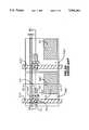
- FIG. 2Aillustrates an example of a top plan view of part of a back plate for a conventional active matrix liquid crystal display of the type previously described
- FIGS. 2B and 2Cillustrate cross-sectional cut-out views of that part of the back plate through lines 2B and 2C, respectively, of FIG. 2A
- the figuresillustrate a top plan view and cross-sectional views of two reflective electrodes, 240' and 340' along with certain circuit elements for driving the two electrodes.
- the figuresare provided for illustrational purposes only, and are not intended to be drawn to scale nor laid out in any particular manner. Common reference numbers in the figures refer to the same elements being depicted.
- the reflective electrodes, 240' and 340', and their respective drive circuitryare formed on the back plate of one type of active matrix liquid crystal display by first forming the drain (e.g., 21') and source (e.g., 23') regions of FETs in a top surface of a silicon substrate 70, and then forming a field oxide layer 71 over the top surface of the silicon substrate 70.
- the field oxide layer 71is then selectively etched away over channel areas (e.g., 24') of the FETs, and a thin oxide layer 72 is then formed over these channel areas (e.g., 24').
- a polysilicon gate bus 100'(also referred to herein as a “row bus” or a “scanning electrode bus”) is then formed along with polysilicon gate electrodes (e.g., 105') and polysilicon storage capacitor electrodes (e.g., 22') for each of the FETs.
- Thisis generally done by a conventional technique of depositing a layer of polysilicon material (also referred to as "polycrystalline silicon” material) over the field oxide layer 71 and the thin oxide layer 72, and then selectively removing portions of that layer so as to leave behind the polysilicon gate bus 100', gate electrodes (e.g., 105'), and storage capacitor electrodes (e.g., 22').
- Another oxide layer 73is then formed over the field oxide layer 71 polysilicon gate bus 100', gate electrodes (e.g., 105'), and storage capacitor electrodes (e.g., 22'). Using conventional techniques, holes (e.g., 25") are then formed in the oxide layers 71 and 73 which extend from the top of the oxide layer 73 down to the drain regions (e.g., 21').
- Column buses(e.g., 210' and 220') (also referred to herein as “signal electrode buses”) are then formed using conventional metallization techniques, along with contacts (e.g., 25') which connect the column buses (e.g., 210') to their proper FET drain regions (e.g., 21').
- oxide layer 74is then formed over the oxide layer 73, as well as over the column buses (e.g., 210' and 220'). Using conventional techniques, holes (e.g., 27" and 242") are then formed in the oxide layers 71, 73 and 74 which extend from the top surface of the oxide layer 74 down to the source regions of the FETs and polysilicon storage capacitor electrodes (e.g., 23' and 22', respectively).
- Reflective electrodese.g., 240' and 340'
- Reflective electrodesare then formed using conventional metallization techniques, along with vias (e.g., 27' and 242') which connect the reflective electrodes (e.g., 240') to their respective source regions and storage capacitor electrodes (e.g., 23' and 22', respectively).
- the storage capacitorsare then completed by grounding the substrate 70 which acts as a second electrode for each of the storage capacitors (e.g., 12 in FIG. 1), and using the field oxide layer 71 as a dielectric medium.
- active matrix liquid crystal displaysmay readily have thousands of such pixels organized in a matrix of rows and columns.
- the resistive and capacitive load built up along the length of a polysilicon gate bussuch as that illustrated as gate bus 100' in FIG. 2A-2C, can cause the last pixel in that row to switch ON and OFF much slower than the first pixel in that row.
- the gate bus 100'might be formed of metal instead of polysilicon material.
- a metal gate buswould require processing a third level of metallization which is very expensive using current processing technology. Not only would a third metallization layer require an additional oxide layer forming step, but it would also require additional photomasking and etching steps to form holes and contacts through the additional oxide layer down to previously deposited gate electrodes formed over the FET channel regions. Such an approach would result in significantly lower yields than the aforedescribed polysilicon gate bus approach.
- one object of the present inventionis to develop a technique and bus structure for driving a row of pixels in an active matrix liquid crystal display along a polysilicon gate bus without the aforedescribed transmission line and resulting non-uniform pixel contrast problems.
- one aspect of the present inventionis a circuit for driving a row of pixels in an active matrix liquid crystal display. Included in the circuit are a plurality of switching elements and a bus structure. Each of the switching elements has a control input and in response to that control input, controls the activation of one of the pixels in the row of pixels. Each of the control inputs is connected to the bus structure so that a row scanning signal transmitted through the bus structure can be concurrently provided to each of the control inputs in order that each of the pixels in the row of pixels can be activated concurrently.
- the bus structurehas a plurality of buffers interspersed among the connections of the control inputs of the plurality of switching elements to the bus structure. These buffers serve to reduce the RC time constants experienced by control inputs whose connections to the bus structure are further away from the source of the row scanning signal and accordingly, serve to enhance uniform contrast between the pixels being activated by the plurality of switching elements. In particular, these buffers are especially useful when the bus structure includes a thin strip of polysilicon as its conductive medium for providing the row scanning signal to each of the control inputs of the plurality of switching elements.
- Another aspect of the present inventionis a method of forming a bus structure for driving a row of pixels in an active matrix liquid crystal display, comprising the steps of: forming a plurality of switching elements including a first portion and a second portion of switching elements, and a plurality of buffers including a first buffer on a substrate, wherein each of the plurality of switching elements has a control input and each of the plurality of buffers has an input and an output; forming a first strip of polysilicon on the substrate, and connecting the control inputs of the first portion of switching elements and the input of the first buffer to the first strip of polysilicon; and forming a second strip of polysilicon on the substrate, and connecting the control inputs of the second portion of switching elements and the output of the first buffer to the second strip of polysilicon; wherein the steps of forming the first and second strips of polysilicon are generally conducted concurrently.
- Still another aspect of the present inventionis a structure for driving four successive pixels in a row of pixels of an active matrix liquid crystal display.
- the structureincludes four field effect transistors ("FETs") and a buffer formed on a silicon substrate, wherein each FET drives one of the four successive pixels.
- FETsfield effect transistors
- a first strip of polysiliconprovides a row scanning signal to gate electrodes of the first and second FETs and an input to the buffer, and a second strip of polysilicon provides the output of the buffer to gate electrodes of the third and fourth FETs.
- the first pixel of the four successive pixelsis formed above and thus covers the first and second FETs
- the second pixelis formed above and thus covers a portion of the buffer
- the third pixelis formed above and thus covers the remaining portion of the buffer
- the fourth pixelis formed above and thus covers the third and fourth FETs.
- the bufferis preferably comprised of two inverters connected in series. Both inverters are preferably comprised of a p-channel and n-channel field effect transistor.
- the portion of the buffer covered by the second pixelis preferably the two n-channel field effect transistors and a small part of the two p-channel transistors, and the remaining portion of the buffer covered by the third pixel is preferably the remaining portions of the two p-channel field effect transistors.
- FIG. 1illustrates a portion of a conventional circuit used for activating selected pixels in a matrix array of pixels in an active matrix liquid crystal display
- FIG. 2Aillustrates an example of a top plan view of part of a back plate for a conventional active matrix liquid crystal display of the type described in reference to FIG. 1;
- FIGS. 2B-2Cillustrate cross-sectional views of that part of the back plate illustrated in FIG. 2A through dotted lines 2B and 2C in FIG. 2A;
- FIG. 3illustrates an example of a portion of a circuit utilizing aspects of the present invention for activating selected pixels in a matrix array of pixels in an active matrix liquid crystal display
- FIG. 4illustrates a preferred embodiment of a buffer which is used in the circuit described in reference to FIG. 3, utilizing aspects of the present invention
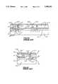
- FIG. 5schematically illustrates four successive pixels and parts of circuitry formed beneath each of the four successive pixels as part of a structure utilizing aspects of the present invention
- FIG. 6shows simulated voltage responses at a 1st and 640th connection to a polysilicon gate bus
- FIG. 7shows simulated voltage responses at a 1st and 640th connection to a polysilicon gate bus having spaced apart buffers.
- FIG. 6two plots are shown. Both plots result from a computer simulation of a polysilicon gate bus having a width W of 3 microns (" ⁇ m") and a length sufficient to drive a row of 640 pixels at a 20 ⁇ m pixel pitch, wherein each of the 640 pixels has a field effect transistor (“FET”) associated with it which serves to activate that pixel, and each of the FETs has a gate electrode connected to the polysilicon gate bus, a drain connected to a signal electrode bus, and a source connected to both a storage capacitor electrode and a reflective electrode of the type described in reference to FIGS. 2A-2C.
- FETfield effect transistor
- Plot 1shows the voltage response at the gate electrode of a 1st FET which drives a 1st pixel in the row of 640 pixels
- plot 2shows the voltage response at the gate electrode of a 640th FET which drives a 640th pixel in the row of 640 pixels.
- ⁇ secmicroseconds
- the problem with the voltage response as shown in plot 2is that a 3.94 ⁇ sec response time far exceeds a maximum response time of 500 nanoseconds which is believed to be the slowest acceptable response time for providing flicker-free operation and reasonably uniform contrast between each of the pixels in the row of pixels. Since the voltage responses at the gate electrode connections in-between the 1st and 640th gate electrode connections are expected to respond proportionally between those calculated for the 1st and 640th, the voltage responses of many of these gate electrode connections are also expected to exceed the maximum response time of 500 nanoseconds.
- FIG. 3illustrates part of a circuit utilizing aspects of the present invention for activating selected pixels organized in a matrix array of rows and columns in an active matrix liquid crystal display (“AMLCD").
- AMLCDactive matrix liquid crystal display
- a plurality of bufferse.g., 1000 and 1001 are interspersed between gate electrode contacts (e.g., 1" to n", n+1" to 2n", etc.) of the FETs (e.g., 1 to n, n+1 to 2n, etc., respectively) associated with each of the pixels (e.g., 1' to n', n+1' to 2n', etc., respectively) in the row of pixels.
- FIG. 4illustrates a preferred embodiment of each of the buffers (e.g., 1000) as used in FIG. 3.
- the buffer 1000has an input I and an output O, and comprises two inverters connected together in series.
- the first invertercomprises a p-channel FET P1 and an n-channel FET N1, and operates such that when the input I is a HIGH logic level, the p-channel FET P1 turns OFF and the n-channel FET N1 turns ON, thus pushing the output OI of the first inverter down to GRND, which acts as a LOW logic level.
- the p-channel FET P1turns ON and the n-channel FET N1 turns OFF, thus pulling the output OI of the first inverter up to Vcc, which acts as a HIGH logic level.
- the output OI of the combination of p-channel FET P1 and n-channel FET N1acts to invert the input I to the buffer 1000.
- the second invertercomprises a p-channel FET P2 and an n-channel FET N2, and operates such that when the output OI of the first inverter is a LOW logic level, the p-channel FET P2 turns ON and the n-channel FET N2 turns OFF, thus pulling the output O of the buffer 1000 up to Vcc, which acts as a HIGH logic level, and when the output OI of the first inverter is a HIGH logic level, the p-channel FET P2 turns OFF and the n-channel FET N2 turns ON, thus pushing the output O of the buffer 1000 down to GRND, which acts as a LOW logic level.
- the output O of the buffer 1000is LOW when its input I is LOW
- the output 0 of the buffer 1000is HIGH when its input I is HIGH.
- the buffers (e.g., 1000 and 1001) interspersed along the polysilicon gate bus (e.g., 100")serve to regenerate the row scanning signal (e.g., 5") after it has been "weakened” by the distributed resistive and capacitive loads along the length of the polysilicon gate bus (e.g., 100").
- the response times at the gate electrode connections to the polysilicon gate bus (e.g., 100")speed up accordingly.
- the propagation time t p of the row scanning signal 5" as it travels along the polysilicon gate bus(e.g., 100") can be calculated from the following well known equation: (See, e.g., Weste, Neil H. E., et. al., Principles of CMOS VLSI Design, Addison-Wesley Publishing Company, 1985, pp. 131-134).
- rresistance per unit length
- ccapacitance per unit length
- 1length of the polysilicon gate bus
- the propagation delay t p ' to a 640th gate electrode connection to the buscan be calculated approximately by the following equation:
- FIG. 7illustrates the results of a computer simulation using a polysilicon gate bus with interspersed buffers attached to the bus, and a row pixel structure similar to that as simulated in reference to FIG. 6.
- plot 2shows that the time required for the voltage at the 640th gate electrode connection to reach 99% of the full charge level of 5.0 volts is only 192 nanoseconds. This is significantly faster than the 3.94 ⁇ sec experienced without the buffers, and is well below the maximum response time of 500 nanoseconds which is believed to be required to provide flicker-free and uniform contrast operation across the row of pixels.
- FIG. 5schematically illustrates four successive pixels (wherein "pixel” is used synonymously with “reflective electrode” for the purposes of describing the present invention) and parts of circuitry formed beneath each of the four successive pixels as part of a structure utilizing aspects of the present invention.
- pixelis used synonymously with “reflective electrode” for the purposes of describing the present invention
- circuitryformed beneath each of the four successive pixels as part of a structure utilizing aspects of the present invention.
- these two switching elements, SE1 and SE2are n-channel FETs whose gates (e.g., "control inputs") are both connected to a polysilicon gate bus segment GB1 in a similar manner as depicted in FIG.
- the polysilicon gate bus segment GB1is connected at one end to the input I of a buffer.
- this first portion of the buffercomprises two n-channel FETs, N1 and N2, corresponding to the two n-channel FETs of the same designation in FIG. 4.
- a ground busruns parallel to the signal electrode buses connected to the drains of the pixel switching elements (e.g., SE1-SE4), and extends under the second pixel PX2.
- this second portion of the buffercomprises two p-channel FETs, P1 and P2, corresponding to the two p-channel FETs of the same designation in FIG. 4.
- design constraintsmay require a small portion of the two p-channel FETs, P1 and P2, to extend under the second pixel PX1.
- a supply busruns parallel to the signal electrode buses connected to the drains of the pixel switching elements (e.g., SE1-SE4), and extends under the third pixel PX3.
- these two switching elements, SE3 and SE4are n-channel FETs whose gates are both connected to a polysilicon gate bus segment GB2, and whose sources are connected to their respective pixels, PX3 and PX4, at connections PC3 and PC4, respectively.
- the polysilicon gate bus segment GB2is connected at one end to the output 0 of the buffer formed under pixels PX2 and PX3.
Landscapes
- Engineering & Computer Science (AREA)
- Chemical & Material Sciences (AREA)
- Crystallography & Structural Chemistry (AREA)
- Physics & Mathematics (AREA)
- Computer Hardware Design (AREA)
- General Physics & Mathematics (AREA)
- Theoretical Computer Science (AREA)
- Liquid Crystal (AREA)
- Liquid Crystal Display Device Control (AREA)
Abstract
Description
t.sub.p =(rcl.sup.2)/2 (1)
t.sub.p '=(rc/2)*(1.sub.1.sup.2 +1.sub.2.sup.2 +1.sub.3.sup.2 +. . . )+t.sub.buf1 +t.sub.buf2 +t.sub.buf3 +. . . (2)
Claims (4)
Priority Applications (4)
| Application Number | Priority Date | Filing Date | Title |
|---|---|---|---|
| US08/022,665US5396261A (en) | 1993-03-01 | 1993-03-01 | Polysilicon gate bus with interspersed buffers for driving a row of pixels in an active matrix liquid crystal display |
| US08/170,394US5396262A (en) | 1993-03-01 | 1993-12-20 | Polysilicon gate bus with interspersed buffers for driving a row of pixels in an active matrix liquid crystal display |
| AU63533/94AAU6353394A (en) | 1993-03-01 | 1994-02-23 | Polysilicon gate bus with interspersed |
| PCT/US1994/002064WO1994020949A1 (en) | 1993-03-01 | 1994-02-23 | Polysilicon gate bus with interspersed buffers |
Applications Claiming Priority (1)
| Application Number | Priority Date | Filing Date | Title |
|---|---|---|---|
| US08/022,665US5396261A (en) | 1993-03-01 | 1993-03-01 | Polysilicon gate bus with interspersed buffers for driving a row of pixels in an active matrix liquid crystal display |
Related Child Applications (1)
| Application Number | Title | Priority Date | Filing Date |
|---|---|---|---|
| US08/170,394DivisionUS5396262A (en) | 1993-03-01 | 1993-12-20 | Polysilicon gate bus with interspersed buffers for driving a row of pixels in an active matrix liquid crystal display |
Publications (1)
| Publication Number | Publication Date |
|---|---|
| US5396261Atrue US5396261A (en) | 1995-03-07 |
Family
ID=21810788
Family Applications (2)
| Application Number | Title | Priority Date | Filing Date |
|---|---|---|---|
| US08/022,665Expired - Fee RelatedUS5396261A (en) | 1993-03-01 | 1993-03-01 | Polysilicon gate bus with interspersed buffers for driving a row of pixels in an active matrix liquid crystal display |
| US08/170,394Expired - LifetimeUS5396262A (en) | 1993-03-01 | 1993-12-20 | Polysilicon gate bus with interspersed buffers for driving a row of pixels in an active matrix liquid crystal display |
Family Applications After (1)
| Application Number | Title | Priority Date | Filing Date |
|---|---|---|---|
| US08/170,394Expired - LifetimeUS5396262A (en) | 1993-03-01 | 1993-12-20 | Polysilicon gate bus with interspersed buffers for driving a row of pixels in an active matrix liquid crystal display |
Country Status (3)
| Country | Link |
|---|---|
| US (2) | US5396261A (en) |
| AU (1) | AU6353394A (en) |
| WO (1) | WO1994020949A1 (en) |
Cited By (17)
| Publication number | Priority date | Publication date | Assignee | Title |
|---|---|---|---|---|
| US5546204A (en)* | 1994-05-26 | 1996-08-13 | Honeywell Inc. | TFT matrix liquid crystal device having data source lines and drain means of etched and doped single crystal silicon |
| US5920298A (en)* | 1996-12-19 | 1999-07-06 | Colorado Microdisplay, Inc. | Display system having common electrode modulation |
| US5959598A (en)* | 1995-07-20 | 1999-09-28 | The Regents Of The University Of Colorado | Pixel buffer circuits for implementing improved methods of displaying grey-scale or color images |
| US6046716A (en) | 1996-12-19 | 2000-04-04 | Colorado Microdisplay, Inc. | Display system having electrode modulation to alter a state of an electro-optic layer |
| US6064364A (en)* | 1993-12-27 | 2000-05-16 | Sharp Kabushiki Kaisha | Image display scanning circuit with outputs from sequentially switched pulse signals |
| US6078303A (en) | 1996-12-19 | 2000-06-20 | Colorado Microdisplay, Inc. | Display system having electrode modulation to alter a state of an electro-optic layer |
| US20010033265A1 (en)* | 2000-03-01 | 2001-10-25 | Yasuyuki Mishima | Liquid crystal display device |
| US20030016202A1 (en)* | 2001-07-13 | 2003-01-23 | Koninklijke Philips Electronics N. V. | Active matrix array devices |
| US20030090478A1 (en)* | 1995-07-20 | 2003-05-15 | The Regents Of The University Of Colorado | Pixel buffer circuits for implementing improved methods of displaying grey-scale or color images |
| US20030193494A1 (en)* | 1999-07-21 | 2003-10-16 | Semiconductor Energy Laboratory Co., Ltd. | Display device |
| US20090121973A1 (en)* | 2007-11-08 | 2009-05-14 | Hyung-Soo Kim | Display device and method of fabricating the same |
| CN102436790A (en)* | 2011-03-23 | 2012-05-02 | 友达光电股份有限公司 | Active matrix electroluminescent display device and driving method thereof |
| CN107274826A (en)* | 2017-03-29 | 2017-10-20 | 友达光电股份有限公司 | Display device |
| WO2018196471A1 (en)* | 2017-04-25 | 2018-11-01 | 京东方科技集团股份有限公司 | Display panel and display device |
| US10424602B2 (en) | 2017-05-12 | 2019-09-24 | Au Optronics Corporation | Display panel |
| US10565922B2 (en) | 2016-10-28 | 2020-02-18 | Au Optronics Corporation | Display panel and display wall |
| US10573221B2 (en) | 2017-09-20 | 2020-02-25 | Au Optronics Corporation | Display apparatus |
Families Citing this family (9)
| Publication number | Priority date | Publication date | Assignee | Title |
|---|---|---|---|---|
| JPH07325323A (en)* | 1994-06-02 | 1995-12-12 | Matsushita Electric Ind Co Ltd | Liquid crystal display |
| US6008874A (en)* | 1995-03-27 | 1999-12-28 | Sanyo Electric Co., Ltd. | Active matrix liquid crystal display having alignment film with inclined surface |
| JP3213540B2 (en)* | 1995-03-27 | 2001-10-02 | 三洋電機株式会社 | Active matrix type liquid crystal display |
| US6372534B1 (en)* | 1995-06-06 | 2002-04-16 | Lg. Philips Lcd Co., Ltd | Method of making a TFT array with photo-imageable insulating layer over address lines |
| US5994721A (en)* | 1995-06-06 | 1999-11-30 | Ois Optical Imaging Systems, Inc. | High aperture LCD with insulating color filters overlapping bus lines on active substrate |
| JP4984731B2 (en)* | 2006-08-09 | 2012-07-25 | セイコーエプソン株式会社 | Matrix type electro-optical device |
| JP5301201B2 (en)* | 2007-06-29 | 2013-09-25 | 株式会社ジャパンディスプレイウェスト | Display device, driving method thereof, and electronic apparatus |
| US8976103B2 (en)* | 2007-06-29 | 2015-03-10 | Japan Display West Inc. | Display apparatus, driving method for display apparatus and electronic apparatus |
| JP2020012977A (en)* | 2018-07-18 | 2020-01-23 | 株式会社ジャパンディスプレイ | Display device |
Citations (12)
| Publication number | Priority date | Publication date | Assignee | Title |
|---|---|---|---|---|
| US3862360A (en)* | 1973-04-18 | 1975-01-21 | Hughes Aircraft Co | Liquid crystal display system with integrated signal storage circuitry |
| US4024626A (en)* | 1974-12-09 | 1977-05-24 | Hughes Aircraft Company | Method of making integrated transistor matrix for flat panel liquid crystal display |
| US4103297A (en)* | 1976-12-20 | 1978-07-25 | Hughes Aircraft Company | Light-insensitive matrix addressed liquid crystal display system |
| US4191452A (en)* | 1977-12-28 | 1980-03-04 | Hughes Aircraft Company | AC silicon PN junction photodiode light-valve substrate |
| US4239346A (en)* | 1979-05-23 | 1980-12-16 | Hughes Aircraft Company | Compact liquid crystal display system |
| US4382658A (en)* | 1980-11-24 | 1983-05-10 | Hughes Aircraft Company | Use of polysilicon for smoothing of liquid crystal MOS displays |
| US4432610A (en)* | 1980-02-22 | 1984-02-21 | Tokyo Shibaura Denki Kabushiki Kaisha | Liquid crystal display device |
| US4602850A (en)* | 1984-03-08 | 1986-07-29 | Vidium, Inc. | Light valve display having integrated driving circuits and shield electrode |
| US4839707A (en)* | 1987-08-27 | 1989-06-13 | Hughes Aircraft Company | LCMOS displays fabricated with implant treated silicon wafers |
| JPH03257427A (en)* | 1990-03-08 | 1991-11-15 | Hitachi Ltd | Liquid crystal display device |
| US5165075A (en)* | 1990-12-10 | 1992-11-17 | Semiconductor Energy Laboratory Co., Ltd. | Electro-optic device having pairs of complementary transistors |
| US5252957A (en)* | 1990-11-15 | 1993-10-12 | Kabushiki Kaisha Toshiba | Sample-and-hold circuit and liquid crystal display apparatus |
- 1993
- 1993-03-01USUS08/022,665patent/US5396261A/ennot_activeExpired - Fee Related
- 1993-12-20USUS08/170,394patent/US5396262A/ennot_activeExpired - Lifetime
- 1994
- 1994-02-23WOPCT/US1994/002064patent/WO1994020949A1/enactiveApplication Filing
- 1994-02-23AUAU63533/94Apatent/AU6353394A/ennot_activeAbandoned
Patent Citations (12)
| Publication number | Priority date | Publication date | Assignee | Title |
|---|---|---|---|---|
| US3862360A (en)* | 1973-04-18 | 1975-01-21 | Hughes Aircraft Co | Liquid crystal display system with integrated signal storage circuitry |
| US4024626A (en)* | 1974-12-09 | 1977-05-24 | Hughes Aircraft Company | Method of making integrated transistor matrix for flat panel liquid crystal display |
| US4103297A (en)* | 1976-12-20 | 1978-07-25 | Hughes Aircraft Company | Light-insensitive matrix addressed liquid crystal display system |
| US4191452A (en)* | 1977-12-28 | 1980-03-04 | Hughes Aircraft Company | AC silicon PN junction photodiode light-valve substrate |
| US4239346A (en)* | 1979-05-23 | 1980-12-16 | Hughes Aircraft Company | Compact liquid crystal display system |
| US4432610A (en)* | 1980-02-22 | 1984-02-21 | Tokyo Shibaura Denki Kabushiki Kaisha | Liquid crystal display device |
| US4382658A (en)* | 1980-11-24 | 1983-05-10 | Hughes Aircraft Company | Use of polysilicon for smoothing of liquid crystal MOS displays |
| US4602850A (en)* | 1984-03-08 | 1986-07-29 | Vidium, Inc. | Light valve display having integrated driving circuits and shield electrode |
| US4839707A (en)* | 1987-08-27 | 1989-06-13 | Hughes Aircraft Company | LCMOS displays fabricated with implant treated silicon wafers |
| JPH03257427A (en)* | 1990-03-08 | 1991-11-15 | Hitachi Ltd | Liquid crystal display device |
| US5252957A (en)* | 1990-11-15 | 1993-10-12 | Kabushiki Kaisha Toshiba | Sample-and-hold circuit and liquid crystal display apparatus |
| US5165075A (en)* | 1990-12-10 | 1992-11-17 | Semiconductor Energy Laboratory Co., Ltd. | Electro-optic device having pairs of complementary transistors |
Non-Patent Citations (5)
| Title |
|---|
| "Capacitance Estimation," Chapter 4, pp. 131-134. |
| "Liquid Crystal MOS Matrix High Density Program," by Bleha et al., Final Technical Report, prepared for U.S. Army, Sep. 1, 1981, AD-A152987. |
| Capacitance Estimation, Chapter 4, pp. 131 134.* |
| Liquid Crystal MOS Matrix High Density Program, by Bleha et al., Final Technical Report, prepared for U.S. Army, Sep. 1, 1981, AD A152987.* |
| Liquid Crystal TV Displays: Principles and Applications . . . , by E. Kaneko, D. Reidel Publishing Company, KTK Scientific Publishers/Tokyo, Chapter 7.* |
Cited By (38)
| Publication number | Priority date | Publication date | Assignee | Title |
|---|---|---|---|---|
| US6064364A (en)* | 1993-12-27 | 2000-05-16 | Sharp Kabushiki Kaisha | Image display scanning circuit with outputs from sequentially switched pulse signals |
| US5546204A (en)* | 1994-05-26 | 1996-08-13 | Honeywell Inc. | TFT matrix liquid crystal device having data source lines and drain means of etched and doped single crystal silicon |
| US6225991B1 (en) | 1995-07-20 | 2001-05-01 | The Regents Of The University Of Colorado | Pixel buffer circuits for implementing improved methods of displaying grey-scale or color images |
| US6452589B1 (en) | 1995-07-20 | 2002-09-17 | The Regents Of The University Of Colorado | Pixel buffer circuits for implementing improved methods of displaying grey-scale or color images |
| US5959598A (en)* | 1995-07-20 | 1999-09-28 | The Regents Of The University Of Colorado | Pixel buffer circuits for implementing improved methods of displaying grey-scale or color images |
| US20030090478A1 (en)* | 1995-07-20 | 2003-05-15 | The Regents Of The University Of Colorado | Pixel buffer circuits for implementing improved methods of displaying grey-scale or color images |
| US6369832B1 (en) | 1995-07-20 | 2002-04-09 | The Regents Of The University Of Colorado | Pixel buffer circuits for implementing improved methods of displaying grey-scale or color images |
| US6295054B1 (en) | 1995-07-20 | 2001-09-25 | The Regents Of The University Of Colorado | Pixel buffer circuits for implementing improved methods of displaying grey-scale or color images |
| US6046716A (en) | 1996-12-19 | 2000-04-04 | Colorado Microdisplay, Inc. | Display system having electrode modulation to alter a state of an electro-optic layer |
| US6144353A (en) | 1996-12-19 | 2000-11-07 | Colorado Microdisplay, Inc. | Display system having electrode modulation to alter a state of an electro-optic layer |
| US6304239B1 (en) | 1996-12-19 | 2001-10-16 | Zight Corporation | Display system having electrode modulation to alter a state of an electro-optic layer |
| US6104367A (en)* | 1996-12-19 | 2000-08-15 | Colorado Microdisplay, Inc. | Display system having electrode modulation to alter a state of an electro-optic layer |
| US6329971B2 (en) | 1996-12-19 | 2001-12-11 | Zight Corporation | Display system having electrode modulation to alter a state of an electro-optic layer |
| US6078303A (en) | 1996-12-19 | 2000-06-20 | Colorado Microdisplay, Inc. | Display system having electrode modulation to alter a state of an electro-optic layer |
| US5920298A (en)* | 1996-12-19 | 1999-07-06 | Colorado Microdisplay, Inc. | Display system having common electrode modulation |
| US8004483B2 (en) | 1999-07-21 | 2011-08-23 | Semiconductor Energy Laboratory Co., Ltd. | Display device |
| US7995015B2 (en) | 1999-07-21 | 2011-08-09 | Semiconductor Energy Laboratory Co., Ltd. | Display device |
| US20030193494A1 (en)* | 1999-07-21 | 2003-10-16 | Semiconductor Energy Laboratory Co., Ltd. | Display device |
| US8669928B2 (en) | 1999-07-21 | 2014-03-11 | Semiconductor Laboratory Co., Ltd. | Display device |
| US7176865B2 (en)* | 1999-07-21 | 2007-02-13 | Semiconductor Energy Laboratory Co., Ltd. | Display device |
| US8362994B2 (en) | 1999-07-21 | 2013-01-29 | Semiconductor Energy Laboratory Co., Ltd. | Display device |
| US20070146265A1 (en)* | 1999-07-21 | 2007-06-28 | Semiconductor Energy Laboratory Co., Ltd. | Display device |
| US20070171164A1 (en)* | 1999-07-21 | 2007-07-26 | Semiconductor Energy Laboratory Co., Ltd. | Display device |
| US20070182678A1 (en)* | 1999-07-21 | 2007-08-09 | Semiconductor Energy Laboratory Co., Ltd. | Display device |
| US8018412B2 (en) | 1999-07-21 | 2011-09-13 | Semiconductor Energy Laboratory Co., Ltd. | Display device |
| US20010033265A1 (en)* | 2000-03-01 | 2001-10-25 | Yasuyuki Mishima | Liquid crystal display device |
| US7230597B2 (en) | 2001-07-13 | 2007-06-12 | Tpo Hong Kong Holding Limited | Active matrix array devices |
| US20030016202A1 (en)* | 2001-07-13 | 2003-01-23 | Koninklijke Philips Electronics N. V. | Active matrix array devices |
| WO2003007286A3 (en)* | 2001-07-13 | 2003-12-24 | Koninkl Philips Electronics Nv | Active matrix array devices |
| TWI405165B (en)* | 2007-11-08 | 2013-08-11 | Samsung Display Co Ltd | Display device |
| CN101430861B (en)* | 2007-11-08 | 2011-03-23 | 三星移动显示器株式会社 | Display device |
| US20090121973A1 (en)* | 2007-11-08 | 2009-05-14 | Hyung-Soo Kim | Display device and method of fabricating the same |
| CN102436790A (en)* | 2011-03-23 | 2012-05-02 | 友达光电股份有限公司 | Active matrix electroluminescent display device and driving method thereof |
| US10565922B2 (en) | 2016-10-28 | 2020-02-18 | Au Optronics Corporation | Display panel and display wall |
| CN107274826A (en)* | 2017-03-29 | 2017-10-20 | 友达光电股份有限公司 | Display device |
| WO2018196471A1 (en)* | 2017-04-25 | 2018-11-01 | 京东方科技集团股份有限公司 | Display panel and display device |
| US10424602B2 (en) | 2017-05-12 | 2019-09-24 | Au Optronics Corporation | Display panel |
| US10573221B2 (en) | 2017-09-20 | 2020-02-25 | Au Optronics Corporation | Display apparatus |
Also Published As
| Publication number | Publication date |
|---|---|
| AU6353394A (en) | 1994-09-26 |
| WO1994020949A1 (en) | 1994-09-15 |
| US5396262A (en) | 1995-03-07 |
Similar Documents
| Publication | Publication Date | Title |
|---|---|---|
| US5396261A (en) | Polysilicon gate bus with interspersed buffers for driving a row of pixels in an active matrix liquid crystal display | |
| EP0362948B1 (en) | Matrix display device | |
| US10304399B2 (en) | Pulse output circuit, shift register, and display device | |
| US5204659A (en) | Apparatus and method for providing a gray scale in liquid crystal flat panel displays | |
| JP3122003B2 (en) | Active matrix substrate | |
| US4114070A (en) | Display panel with simplified thin film interconnect system | |
| US5808595A (en) | Thin-film transistor circuit and image display | |
| EP0079496B1 (en) | Matrix display and driving method therefor | |
| US7522145B2 (en) | Liquid crystal display apparatus | |
| KR100234940B1 (en) | Structure of anti-static liquid crystal display panel and its operation method | |
| US20060071895A1 (en) | Display device having an improved voltage level converter circuit | |
| US5898322A (en) | Logic circuit for liquid crystal display having pass-transistor logic circuitry and thin film transistors | |
| US20110255653A1 (en) | Shift register | |
| JP2000356978A (en) | Data line driving method and liquid crystal display device using the same | |
| US5546204A (en) | TFT matrix liquid crystal device having data source lines and drain means of etched and doped single crystal silicon | |
| KR100655773B1 (en) | Active Matrix Liquid Crystal Display Device | |
| US5619222A (en) | Liquid crystal display device having static electricity removing circuits | |
| CN101004521B (en) | Array substrate, display device having same, and driving method of display device | |
| JP2004513394A (en) | Display device | |
| CN210245031U (en) | Pixel display structure and panel | |
| JP2939043B2 (en) | Active matrix substrate | |
| TW200528793A (en) | Array substrate for flat display device | |
| JP2002090708A (en) | Circuit board and flat panel display | |
| TWI841165B (en) | E-paper display apparatus and driving method of e-paper display panel | |
| CN115273721B (en) | Display panel and display device |
Legal Events
| Date | Code | Title | Description |
|---|---|---|---|
| AS | Assignment | Owner name:WAH-III TECHNOLOGY CORPORATION, CALIFORNIA Free format text:ASSIGNMENT OF ASSIGNORS INTEREST;ASSIGNOR:HASTINGS, WILLIAM A., III;REEL/FRAME:006574/0014 Effective date:19930422 | |
| AS | Assignment | Owner name:ARGYLE CAPITAL MANAGEMENT CORPORATION, NEW YORK Free format text:SECURITY AGREEMENT;ASSIGNOR:SPATIALIGHT, INC.;REEL/FRAME:009027/0760 Effective date:19980224 | |
| AS | Assignment | Owner name:SPATIALIGHT, INC., CALIFORNIA Free format text:ASSIGNMENT OF ASSIGNORS INTEREST;ASSIGNOR:SPATIALIGHT OF CALIFORNIA, INC.;REEL/FRAME:009396/0817 Effective date:19980812 | |
| REMI | Maintenance fee reminder mailed | ||
| AS | Assignment | Owner name:WOODS, ROBERT E., ALABAMA Free format text:SECURITY INTEREST;ASSIGNORS:SPATIALIGHT, INC.;SPATIALIGHT OF CALIFORNIA, INC.;REEL/FRAME:009596/0325 Effective date:19981120 Owner name:SPATLIGHT OF CALIFORNIA, INC., CALIFORNIA Free format text:CHANGE OF NAME;ASSIGNOR:WAH-III TECHNOLOGY CORP.;REEL/FRAME:009596/0230 Effective date:19980627 Owner name:TRIPP, MARCIA K., ALABAMA Free format text:SECURITY INTEREST;ASSIGNORS:SPATIALIGHT, INC.;SPATIALIGHT OF CALIFORNIA, INC.;REEL/FRAME:009596/0325 Effective date:19981120 Owner name:ROLFE, ROBERT O., TENNESSEE Free format text:SECURITY INTEREST;ASSIGNORS:SPATIALIGHT, INC.;SPATIALIGHT OF CALIFORNIA, INC.;REEL/FRAME:009596/0325 Effective date:19981120 Owner name:HARVEY, JIMMIE H., ALABAMA Free format text:SECURITY INTEREST;ASSIGNORS:SPATIALIGHT, INC.;SPATIALIGHT OF CALIFORNIA, INC.;REEL/FRAME:009596/0325 Effective date:19981120 Owner name:LISA MARIE TRIPP TRUST, ALABAMA Free format text:SECURITY INTEREST;ASSIGNORS:SPATIALIGHT, INC.;SPATIALIGHT OF CALIFORNIA, INC.;REEL/FRAME:009596/0325 Effective date:19981120 Owner name:FBO JIMMIE H. HARVEY, M.D. BIRMINGHAM, ALABAMA Free format text:SECURITY INTEREST;ASSIGNORS:SPATIALIGHT, INC.;SPATIALIGHT OF CALIFORNIA, INC.;REEL/FRAME:009596/0325 Effective date:19981120 Owner name:WAYNE PATRICK TRIPP TRUST, ALABAMA Free format text:SECURITY INTEREST;ASSIGNORS:SPATIALIGHT, INC.;SPATIALIGHT OF CALIFORNIA, INC.;REEL/FRAME:009596/0325 Effective date:19981120 Owner name:TRIPP, STEVEN F., AS COLLATERAL AGENT FOR THE LEND Free format text:SECURITY INTEREST;ASSIGNORS:SPATIALIGHT, INC.;SPATIALIGHT OF CALIFORNIA, INC.;REEL/FRAME:009596/0325 Effective date:19981120 Owner name:STARR, BRYAN B. SR., ALABAMA Free format text:SECURITY INTEREST;ASSIGNORS:SPATIALIGHT, INC.;SPATIALIGHT OF CALIFORNIA, INC.;REEL/FRAME:009596/0325 Effective date:19981120 Owner name:HILLIARD LIMITED PARTNERSHIP, WISCONSIN Free format text:SECURITY INTEREST;ASSIGNORS:SPATIALIGHT, INC.;SPATIALIGHT OF CALIFORNIA, INC.;REEL/FRAME:009596/0325 Effective date:19981120 Owner name:WALLACE J. HILLIARD FLINT TRUST, WISCONSIN Free format text:SECURITY INTEREST;ASSIGNORS:SPATIALIGHT, INC.;SPATIALIGHT OF CALIFORNIA, INC.;REEL/FRAME:009596/0325 Effective date:19981120 Owner name:TWIFORD, DAVID A. IRT, TENNESSEE Free format text:SECURITY INTEREST;ASSIGNORS:SPATIALIGHT, INC.;SPATIALIGHT OF CALIFORNIA, INC.;REEL/FRAME:009596/0325 Effective date:19981120 Owner name:EAKIN, JOHN W., TENNESSEE Free format text:SECURITY INTEREST;ASSIGNORS:SPATIALIGHT, INC.;SPATIALIGHT OF CALIFORNIA, INC.;REEL/FRAME:009596/0325 Effective date:19981120 Owner name:STARR, BRYAN B. JR., ALABAMA Free format text:SECURITY INTEREST;ASSIGNORS:SPATIALIGHT, INC.;SPATIALIGHT OF CALIFORNIA, INC.;REEL/FRAME:009596/0325 Effective date:19981120 Owner name:WEYERS, ROBERT J., WISCONSIN Free format text:SECURITY INTEREST;ASSIGNORS:SPATIALIGHT, INC.;SPATIALIGHT OF CALIFORNIA, INC.;REEL/FRAME:009596/0325 Effective date:19981120 Owner name:KING, MATTHEW A., TENNESSEE Free format text:SECURITY INTEREST;ASSIGNORS:SPATIALIGHT, INC.;SPATIALIGHT OF CALIFORNIA, INC.;REEL/FRAME:009596/0325 Effective date:19981120 Owner name:TRIPP, STEVEN FRANCIS, ALABAMA Free format text:SECURITY INTEREST;ASSIGNORS:SPATIALIGHT, INC.;SPATIALIGHT OF CALIFORNIA, INC.;REEL/FRAME:009596/0325 Effective date:19981120 Owner name:WEYERS, RONALD A., WISCONSIN Free format text:SECURITY INTEREST;ASSIGNORS:SPATIALIGHT, INC.;SPATIALIGHT OF CALIFORNIA, INC.;REEL/FRAME:009596/0325 Effective date:19981120 Owner name:COBB, JEFFERSON R., ALABAMA Free format text:SECURITY INTEREST;ASSIGNORS:SPATIALIGHT, INC.;SPATIALIGHT OF CALIFORNIA, INC.;REEL/FRAME:009596/0325 Effective date:19981120 Owner name:KLISTER, PAUL, WISCONSIN Free format text:SECURITY INTEREST;ASSIGNORS:SPATIALIGHT, INC.;SPATIALIGHT OF CALIFORNIA, INC.;REEL/FRAME:009596/0325 Effective date:19981120 Owner name:GIEGER, HOLLIS N., ALABAMA Free format text:SECURITY INTEREST;ASSIGNORS:SPATIALIGHT, INC.;SPATIALIGHT OF CALIFORNIA, INC.;REEL/FRAME:009596/0325 Effective date:19981120 | |
| LAPS | Lapse for failure to pay maintenance fees | ||
| FP | Lapsed due to failure to pay maintenance fee | Effective date:19990307 | |
| AS | Assignment | Owner name:HARVEY, JIMMIE H., AS COLLATERAL AGENT, ALABAMA Free format text:SECURITY AGREEMENT;ASSIGNORS:SPATIALIGHT, INC.;SPATIALIGHT OF CALIFORNIA, INC.;REEL/FRAME:010547/0474 Effective date:19991207 Owner name:WEYERS, RONALD A., WISCONSIN Free format text:SECURITY AGREEMENT;ASSIGNORS:SPATIALIGHT, INC.;SPATIALIGHT OF CALIFORNIA, INC.;REEL/FRAME:010547/0474 Effective date:19991207 Owner name:WEYERS, JEFFREY J., WISCONSIN Free format text:SECURITY AGREEMENT;ASSIGNORS:SPATIALIGHT, INC.;SPATIALIGHT OF CALIFORNIA, INC.;REEL/FRAME:010547/0474 Effective date:19991207 Owner name:WEYERS FAMILY LIMITED PARTNERSHIP, WISCONSIN Free format text:SECURITY AGREEMENT;ASSIGNORS:SPATIALIGHT, INC.;SPATIALIGHT OF CALIFORNIA, INC.;REEL/FRAME:010547/0474 Effective date:19991207 Owner name:ROLFE, ROBERT O., TENNESSEE Free format text:SECURITY AGREEMENT;ASSIGNORS:SPATIALIGHT, INC.;SPATIALIGHT OF CALIFORNIA, INC.;REEL/FRAME:010547/0474 Effective date:19991207 Owner name:EAKIN, JOHN W., TENNESSEE Free format text:SECURITY AGREEMENT;ASSIGNORS:SPATIALIGHT, INC.;SPATIALIGHT OF CALIFORNIA, INC.;REEL/FRAME:010547/0474 Effective date:19991207 Owner name:STARR, BRYAN B., SR., ALABAMA Free format text:SECURITY AGREEMENT;ASSIGNORS:SPATIALIGHT, INC.;SPATIALIGHT OF CALIFORNIA, INC.;REEL/FRAME:010547/0474 Effective date:19991207 Owner name:WOODS, ROBERT E., ALABAMA Free format text:SECURITY AGREEMENT;ASSIGNORS:SPATIALIGHT, INC.;SPATIALIGHT OF CALIFORNIA, INC.;REEL/FRAME:010547/0474 Effective date:19991207 Owner name:TRIPP, MARCIA K., ALABAMA Free format text:SECURITY AGREEMENT;ASSIGNORS:SPATIALIGHT, INC.;SPATIALIGHT OF CALIFORNIA, INC.;REEL/FRAME:010547/0474 Effective date:19991207 Owner name:TRIPP, LISA MARIE (TRUST), ALABAMA Free format text:SECURITY AGREEMENT;ASSIGNORS:SPATIALIGHT, INC.;SPATIALIGHT OF CALIFORNIA, INC.;REEL/FRAME:010547/0474 Effective date:19991207 Owner name:TRIPP, WAYNE P. (TRUST), ALABAMA Free format text:SECURITY AGREEMENT;ASSIGNORS:SPATIALIGHT, INC.;SPATIALIGHT OF CALIFORNIA, INC.;REEL/FRAME:010547/0474 Effective date:19991207 Owner name:TRIPP, STEVEN FRANCIS (TRUST), ALABAMA Free format text:SECURITY AGREEMENT;ASSIGNORS:SPATIALIGHT, INC.;SPATIALIGHT OF CALIFORNIA, INC.;REEL/FRAME:010547/0474 Effective date:19991207 Owner name:HARVEY, JIMMIE H., ALABAMA Free format text:SECURITY AGREEMENT;ASSIGNORS:SPATIALIGHT, INC.;SPATIALIGHT OF CALIFORNIA, INC.;REEL/FRAME:010547/0474 Effective date:19991207 Owner name:HILLIARD LIMITED PARTNERSHIP, WISCONSIN Free format text:SECURITY AGREEMENT;ASSIGNORS:SPATIALIGHT, INC.;SPATIALIGHT OF CALIFORNIA, INC.;REEL/FRAME:010547/0474 Effective date:19991207 Owner name:TWIFORD, DAVID A., TENNESSEE Free format text:SECURITY AGREEMENT;ASSIGNORS:SPATIALIGHT, INC.;SPATIALIGHT OF CALIFORNIA, INC.;REEL/FRAME:010547/0474 Effective date:19991207 Owner name:KLISTER, PAUL, WISCONSIN Free format text:SECURITY AGREEMENT;ASSIGNORS:SPATIALIGHT, INC.;SPATIALIGHT OF CALIFORNIA, INC.;REEL/FRAME:010547/0474 Effective date:19991207 Owner name:COBB, JEFFERSON R., COLORADO Free format text:SECURITY AGREEMENT;ASSIGNORS:SPATIALIGHT, INC.;SPATIALIGHT OF CALIFORNIA, INC.;REEL/FRAME:010547/0474 Effective date:19991207 Owner name:KING, LLEW ANN, TENNESSEE Free format text:SECURITY AGREEMENT;ASSIGNORS:SPATIALIGHT, INC.;SPATIALIGHT OF CALIFORNIA, INC.;REEL/FRAME:010547/0474 Effective date:19991207 Owner name:AGT. C.T. WILLIAMS, TUA 11/1/76, TENNESSEE Free format text:SECURITY AGREEMENT;ASSIGNORS:SPATIALIGHT, INC.;SPATIALIGHT OF CALIFORNIA, INC.;REEL/FRAME:010547/0474 Effective date:19991207 Owner name:PERFORMANCE FUTURES PSP, ALABAMA Free format text:SECURITY AGREEMENT;ASSIGNORS:SPATIALIGHT, INC.;SPATIALIGHT OF CALIFORNIA, INC.;REEL/FRAME:010547/0474 Effective date:19991207 Owner name:BIRMINGHAM HEMATOLOGY AND ONCOLOGY ASSOCIATES, ALA Free format text:SECURITY AGREEMENT;ASSIGNORS:SPATIALIGHT, INC.;SPATIALIGHT OF CALIFORNIA, INC.;REEL/FRAME:010547/0474 Effective date:19991207 Owner name:WEYERS, ROBERT J., WISCONSIN Free format text:SECURITY AGREEMENT;ASSIGNORS:SPATIALIGHT, INC.;SPATIALIGHT OF CALIFORNIA, INC.;REEL/FRAME:010547/0474 Effective date:19991207 Owner name:KING, MATTHEW A., CHARITABLE REMAINDER UNITRUST DT Free format text:SECURITY AGREEMENT;ASSIGNORS:SPATIALIGHT, INC.;SPATIALIGHT OF CALIFORNIA, INC.;REEL/FRAME:010547/0474 Effective date:19991207 | |
| AS | Assignment | Owner name:SPATIALIGHT, INC., CALIFORNIA Free format text:REASSIGNMENT AND RELEASE OF SECURITY INTEREST;ASSIGNOR:TRIPP, STEVEN, AS COLLATERAL AGENT;REEL/FRAME:010756/0311 Effective date:20000419 | |
| FEPP | Fee payment procedure | Free format text:PAT HOLDER CLAIMS SMALL ENTITY STATUS, ENTITY STATUS SET TO SMALL (ORIGINAL EVENT CODE: LTOS); ENTITY STATUS OF PATENT OWNER: SMALL ENTITY | |
| FEPP | Fee payment procedure | Free format text:PETITION RELATED TO MAINTENANCE FEES FILED (ORIGINAL EVENT CODE: PMFP); ENTITY STATUS OF PATENT OWNER: SMALL ENTITY Free format text:PETITION RELATED TO MAINTENANCE FEES DENIED/DISMISSED (ORIGINAL EVENT CODE: PMFD); ENTITY STATUS OF PATENT OWNER: SMALL ENTITY | |
| STCH | Information on status: patent discontinuation | Free format text:PATENT EXPIRED DUE TO NONPAYMENT OF MAINTENANCE FEES UNDER 37 CFR 1.362 | |
| AS | Assignment | Owner name:AMERICAN BANK AND TRUST COMPANY, OKLAHOMA Free format text:ASSIGNMENT OF SECURITY AGMT;ASSIGNOR:ARGYLE CAPITAL MANAGEMENT CORPORATION;REEL/FRAME:014162/0776 Effective date:20030527 Owner name:AMERICAN BANK AND TRUST COMPANY, OKLAHOMA Free format text:ASSIGNMENT OF SECURITY INTEREST;ASSIGNOR:ARGYLE CAPITAL MANAGEMENT CORPORATION;REEL/FRAME:014162/0122 Effective date:20030523 Owner name:AMERICAN BANK AND TRUST COMPANY, OKLAHOMA Free format text:ASSIGNMENT OF SECURITY INTEREST;ASSIGNOR:ARGYLE CAPITAL MANAGEMENT CORPORATION;REEL/FRAME:014172/0875 Effective date:20030523 |